

Designing
Audio Power
Amplifiers
Copyrighted
Material

About the Author
Bob Cordell is an electrical engineer who has been
deeply involved in audio since his adventures with
vacuum tube designs in his teen years. He is an
equal-opportunity designer to this day, having built
amplifiers with vacuum tubes, bipolar transistors, and
MOSFETs. Bob is also a prolific designer of audio test
equipment, including a high-performance THD
analyzer and many purpose-built pieces of audio gear.
He has published numerous articles and papers on
power amplifier design and distortion measurement
in the popular press and in the Journal of the Audio
Engineering Society
. In 1983 he published a power
amplifier design combining vertical power MOSFETs
with error correction, achieving unprecedented
distortion levels of less than 0.001% at 20 kHz.
Bob is also an avid DIY loudspeaker builder, and
has combined this endeavor with his electronic
interests in the design of powered audiophile
loudspeaker systems. He and his colleagues have
presented audiophile listening and measurement
workshops at the Rocky Mountain Audio Fest and
the Home Entertainment Show.
As an electrical engineer, Bob has worked at
Bell Laboratories and other telecommunications
companies, where his work has included design of
integrated circuits and fiber optic communications
systems. He maintains an audiophile website at www
.cordellaudio.com, where diverse material on audio
electronics, loudspeakers, and instrumentation can be
found.
Copyrighted
Material

xxviii
C o n t e n t s
Preface
T
here are several very good books on audio power amplifier design already out
there, so you might ask why we need yet another book on power amplifier
design. Hopefully this preface will answer that question. However, the short
answer can be found in two observations. First, there have been many developments in
audio power amplifier design since the release of most of the prior books. Second, there
are some important topics that deserve more depth of coverage.
Designing Audio Power Amplifiers
is written to address many advanced topics and
important design subtleties. At the same time, however, it has enough introductory and
tutorial coverage to allow designers relatively new to the field to absorb the material of
the book without being overwhelmed. To this end, the book starts off at a relaxing pace
that helps the reader develop an intuitive feel and understanding for amplifier design.
Although this book covers advanced subjects, highly involved mathematics is kept to a
minimum—much of that is left to the academics. Design choices and decisions are
explained and analyzed.
This is not just a cookbook; it is intended to teach the reader how to think about
power amplifier design and understand the many concepts and nuances, then analyze
and synthesize the many possible variations of amplifier design.
I have divided the book into six parts. Part 1 introduces audio power amplifier
design and includes the basics. This part is designed to be readable and friendly to
those with less technical background while still providing a very sound footing for the
more detailed design discussions that follow. In this part I show how a simple power
amplifier design evolves in several steps to a modern architecture, describing how
performance deficiencies are mitigated with circuit improvements at each step in the
evolution. Even experienced designers may gain valuable insights here.
Part 2 delves into the design of advanced power amplifiers with state-of-the art
performance. Crossover distortion, one of the most problematic distortions in power
amplifiers, is covered in depth. Special attention is paid to dynamic crossover distortion,
which is less well understood. This part also includes a detailed treatment of MOSFET
power amplifiers, error correction techniques, advanced feedback compensation, ultra-
low distortion drive circuits, and DC servos.
Part 3 covers those real-world design considerations that influence sound quality
and reliability, including power supplies and grounding, short circuit and safe area
protection, and amplifier behavior when driving difficult loads. Thermal design and
thermal stability are given special attention. Electromagnetic interference ingress and
egress via the input, output, and mains ports of the amplifier are also treated here.
SPICE simulation can be very important to power amplifier design, and its use is
described in detail in Part 4. Even those with no SPICE experience will learn how to
use this valuable tool, helped along by a tutorial chapter and ready-to-run amplifier
simulations and transistor models available at www.cordellaudio.com. A full
chapter describes how you can create your own accurate SPICE models for BJT and
MOSFET transistors, many of which are poorly modeled by manufacturers. Numerous
approaches to distortion measurement are also explained in Part 4. I’ve also described
xxix
Copyrighted
Material

some techniques for achieving the high sensitivity required to measure the low-
distortion designs discussed in the book. Less well-known distortion measurements,
such as TIM, PIM, and IIM, are also covered here. In the quest for meaningful
correspondence between listening and measurement results, other non-traditional
amplifier tests are also described.
Part 5, Topics in Amplifier Design, covers all of those other important matters that
do not fit neatly into the other parts. Advanced designers as well as audiophiles will
find many interesting topics in this part. Some of the controversies in audio, such as the
use of negative feedback, are addressed here. For balance, the design of amplifiers
without negative feedback is covered. Integrated circuit power amplifiers and drivers
are also discussed.
Class D amplifiers are playing a more important role in audio amplification as every
day passes. They have enjoyed vast improvements in performance over the last several
years and can be expected to improve much further in the future. Four chapters in Part 6
cover this exciting technology.
Many of the following topics covered in Designing Audio Power Amplifiers should
prove especially interesting to readers familiar with earlier texts:
• Ultra-lowdistortioninputandvoltageamplifiertopologies
• Non-conventionalfeedbackcompensationtechniques
• LateralandverticalMOSFETpoweramplifiers
• Outputstageerrorcorrectioncircuits
• ThermalstabilityanalysisofBJTandMOSFEToutputstages
• Outputtransistorswithtemperaturetrackingdiodes
• Integratedcircuitamplifiersanddrivers
• SPICEsimulationandmodelingforamplifierdesign
• Amplifiermeasurementinstrumentationandtechniques
• PC-basedinstrumentationforamplifierevaluation
• Howamplifiersmisbehaveandwhytheysounddifferent
• SourcesofdistortioninclassDamplifiers
• PWM,sigma-delta,anddirectdigitalclassDamplifiers
No single text can cover all aspects of audio power amplifier design. It is my hope
that an experienced designer or a hobbyist who seeks to learn more about audio
amplifier design will find this book most helpful. I also hope that this text will provide
a sound basis for those wishing to learn analog circuit design.
Bob Cordell
xxx
P r e f a c e
xxxi
Copyrighted
Material

15
CHAPTER
2
Power Amplifier Basics
I
n this chapter we’ll look at the design of a basic power amplifier in detail. Some
information about transistors will first be discussed, followed by a simple analysis
of the basic building block circuits that are inevitably used to build a complete
amplifier circuit. This will provide a good foundation for the detailed analysis of the
basic amplifier that follows. Chapter 3 will then take us on a tour of amplifier design,
evolving and assessing a design as its performance is improved to a high level.
2.1 About Transistors
The bipolar junction transistor (BJT) is the primary building block of most audio power
amplifiers. This section is not meant to be an exhaustive review of transistors, but rather
presents enough knowledge for you to understand and analyze transistor amplifier
circuits. More importantly, transistor behavior is discussed in the context of power
amplifier design, with many relevant tips along the way.
Current Gain
If a small current is sourced into the base of an NPN transistor, a much larger current
flows in the collector. The ratio of these two currents is the current gain, commonly
called beta (
β) or h
fe
. Similarly, if one sinks a small current from the base of a PNP transis-
tor, a much larger current flows in its collector.
The current gain for a typical small-signal transistor often lies between 50 and 200.
For an output transistor,
β typically lies between 20 and 100. Beta can vary quite a bit
from transistor to transistor and is also a mild function of the transistor current and col-
lector voltage.
Because transistor
β can vary quite a bit, circuits are usually designed so that their
operation does not depend heavily on the particular value of
β for its transistors. Rather,
the circuit is designed so that it operates well for a minimum value of
β and better for
very high
β. Because β can sometimes be very high, it is usually bad practice to design
a circuit that would misbehave if
β became very high. The transconductance (gm) of the
transistor is actually the more predictable and important design parameter (as long as
β is high enough not to matter much). For those unfamiliar with the term, transconduc-
tance of a transistor is the change in collector current in response to a given change in
base-emitter voltage, in units of siemens (S; amps per volt).
gm
= ∆I
c
/
∆V
be
The familiar collector current characteristics shown in Figure 2.1 illustrate the
behavior of transistor current gain. This family of curves shows how the collector current
Copyrighted
Material
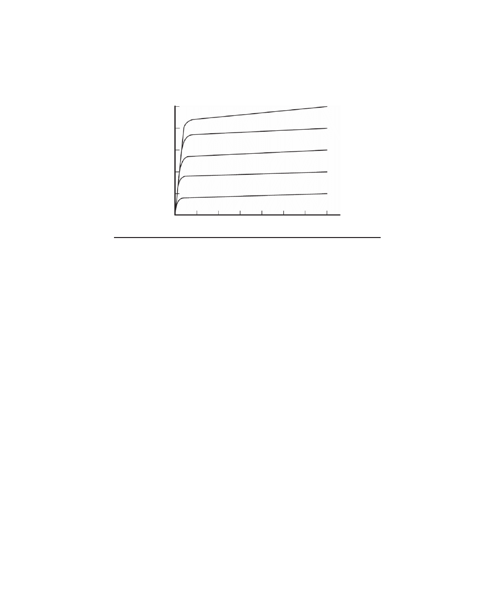
16
A u d i o P o w e r A m p l i f i e r B a s i c s
P o w e r A m p l i f i e r B a s i c s
17
increases as collector-emitter voltage (V
ce
) increases, with base current as a parameter.
The upward slope of each curve with increasing V
ce
reveals the mild dependence of
β
on collector-emitter voltage. The spacing of the curves for different values of base cur-
rent reveals the current gain. Notice that this spacing tends to increase as V
ce
increases,
once again revealing the dependence of current gain on V
ce
. The spacing of the curves
may be larger or smaller between different pairs of curves. This illustrates the depen-
dence of current gain on collector current. The transistor shown has
β of about 50.
Beta can be a strong function of current when current is high; it can decrease
quickly with increases in current. This is referred to as beta droop and can be a source of
distortion in power amplifiers. A typical power transistor may start with a
β of 70 at
a collector current of 1 A and have its
β fall to 20 or less by the time I
c
reaches 10 A. This
is especially important when the amplifier is called on to drive low load impedances.
This is sobering in light of the current requirements illustrated in Table 1.3.
Base-Emitter Voltage
The bipolar junction transistor requires a certain forward bias voltage at its base-emitter
junction to begin to conduct collector current. This turn-on voltage is usually referred to
as V
be
. For silicon transistors, V
be
is usually between 0.5 and 0.7 V. The actual value of
V
be
depends on the transistor device design and the amount of collector current (I
c
).
The base-emitter voltage increases by about 60 mV for each decade of increase in
collector current. This reflects the logarithmic relationship of V
be
to collector current.
For the popular 2N5551, for example, V
be
= 600 mV at 100 µA and rises to 720 mV at
10 mA. This corresponds to a 120 mV increase for a two-decade (100:1) increase in
collector current.
Tiny amounts of collector current actually begin to flow at quite low values of for-
ward bias (V
be
). Indeed, the collector current increases exponentially with V
be
. That is
why it looks like there is a fairly well-defined turn-on voltage when collector current is
plotted against V
be
on linear coordinates. It becomes a remarkably straight line when
25 mA
20 mA
15 mA
10 mA
I
c
5 mA
0 mA
0 V
1 V
2 V
3 V
4 V
V
ce
5 V
6 V
7 V
0.1 mA
0.2 mA
0.3 mA
0.4 mA
0.5 mA
F
igure
2.1 Transistor collector current characteristic.
Copyrighted
Material

16
A u d i o P o w e r A m p l i f i e r B a s i c s
P o w e r A m p l i f i e r B a s i c s
17
the log of collector current is plotted against V
be
. Some circuits, like multipliers, make
great use of this logarithmic dependence of V
be
on collector current.
Put another way, the collector current increases exponentially with base-emitter
voltage, and we have the approximation
I
I e
c
S
V
V
T
=
(
/ )
be
where the voltage V
T
is called the thermal voltage. Here V
T
is about 26 mV at room tem-
perature and is proportional to absolute temperature. This plays a role in the tempera-
ture dependence of V
be
. However, the major cause of the temperature dependence of V
be
is the strong increase with temperature of the saturation current I
S
. This ultimately results
in a negative temperature coefficient of V
be
of about
-2.2 mV/°C.
Expressing base-emitter voltage as a function of collector current, we have the anal-
ogous approximation
V
be
= V
T
ln (I
c
/I
S
)
where ln (I
c
/I
S
) is the natural logarithm of the ratio I
c
/I
S
. The value of V
be
here is the
intrinsic
base-emitter voltage, where any voltage drops across physical base resistance
and emitter resistance are not included.
The base-emitter voltage for a given collector current typically decreases by about
2.2 mV for each degree Celsius increase in temperature. This means that when a transis-
tor is biased with a fixed value of V
be
, the collector current will increase as temperature
increases. As collector current increases, so will the power dissipation and heating of the
transistor; this will lead to further temperature increases and sometimes a vicious cycle
called thermal runaway. This is essentially positive feedback in a local feedback system.
The V
be
of power transistors will start out at a smaller voltage at a low collector cur-
rent of about 100 mA, but may increase substantially to 1 V or more at current in the 1
to 10-A range. At currents below about 1 A, V
be
typically follows the logarithmic rule,
increasing by about 60 mV per decade of increase in collector current. As an example,
V
be
might increase from 550 mV at 150 mA to 630 mV at 1 A. Even this is more than
60 mV per decade.
Above about 1 A, V
be
versus I
c
for a power transistor often begins to behave linearly
like a resistance. In the same example, V
be
might increase to about 1.6 V at 1 A. This
would correspond to effectively having a resistance of about 0.1
Ω in series with the
emitter. The actual emitter resistance is not necessarily the physical origin of the increase
in V
be
. The voltage drop across the base resistance RB due to base current is often more
significant. This voltage drop will be equal to RB(I
c
/
β). The effective contribution to
resistance as seen at the emitter by RB is thus RB/
β. The base resistance divided by β is
often the dominant source of this behavior.
Consider a power transistor operating at I
c
= 10 A and having a base resistance of 4 Ω,
an operating
β of 50, and an emitter resistance of 20 mΩ. Base current will be 200 mA
and voltage drop across the base resistance will be 0.8 V. Voltage drop across the emitter
resistance will be 0.2 V. Adding the intrinsic V
be
of perhaps 660 mV, the base-emitter
voltage becomes 1.66 V. It is thus easy to see how rather high V
be
can develop for power
transistors at high operating currents.
The Gummel Plot
If the log of collector current is plotted as a function of V
be
, the resulting diagram is very
revealing. As mentioned above, it is ideally a straight line. The diagram becomes even
Copyrighted
Material
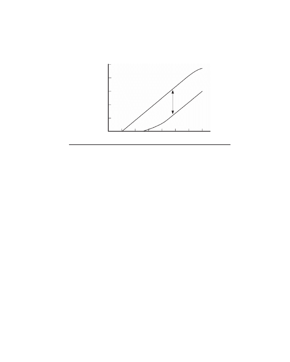
18
A u d i o P o w e r A m p l i f i e r B a s i c s
P o w e r A m p l i f i e r B a s i c s
19
more useful and insightful if base current is plotted on the same axes. This is now called
a Gummel plot. It sounds fancy, but that is all it is. The magic lies in what it reveals about
the transistor. A Gummel plot is shown in Figure 2.2.
In practice, neither the collector current nor the base current plots are straight lines
over the full range of V
be
, and the bending illustrates various nonidealities in the tran-
sistor behavior. The vertical distance between the lines corresponds to the
β of the tran-
sistor, and the change in distance shows how
β changes as a function of V
be
and, by
extension, I
c
. The curves in Figure 2.2 illustrate the typical loss in transistor current gain
at both low and high current extremes.
Transconductance
While transistor current gain is an important parameter and largely the source of its
amplifying ability, the transconductance of the transistor is perhaps the most important
characteristic used by engineers when doing actual design. Transconductance, denoted
as gm, is the ratio of the change in collector current to the change in base voltage.
The unit of measure of transconductance is the siemens (S), which corresponds to a
current change of 1 A for a change of 1 V. This is the inverse of the measure of resistance,
the ohm (it was once called the mho, ohm spelled backward). If the base-emitter voltage
of a transistor is increased by 1 mV, and as a result the collector current increases by
40
µA, the transconductance of the transistor is 40 milliseimens (mS).
The transconductance of a bipolar transistor is governed by its collector current.
This is a direct result of the exponential relationship of collector current to base-emitter
voltage. The slope of that curve increases as I
c
increases; this means that transconduc-
tance also increases. Transconductance is given simply as
gm
= I
c
/V
T
where V
T
is the thermal voltage, typically 26 mV at room temperature. At a current of
1 mA, transconductance is 1 mA/26 mV
= 0.038 S.
100 mA
10 mA
1 mA
100 µA
I
c
I
c
I
b
10 µA
1 µA
0.40 V 0.45 V 0.50 V 0.55 V 0.60 V
V
be
0.65 V
β = 100
0.70 V 0.75 V
F
igure
2.2 Transistor Gummel plot.
Copyrighted
Material

18
A u d i o P o w e r A m p l i f i e r B a s i c s
P o w e r A m p l i f i e r B a s i c s
19
The inverse of gm is a resistance. Sometimes it is easier to visualize the behavior of
a circuit by treating the transconductance of the transistor as if it were a built-in dynamic
emitter resistance re
′. This resistance is just the inverse of gm, so we have
re
′ = V
T
/I
c
= 0.026/I
c
(at room temperature)
In the above case re
′ = 26 Ω at a collector current of 1 mA.
An important approximation that will be used frequently is that re
′ = 26 Ω/I
c
where
I
c
is expressed in milliamperes. If a transistor is biased at 10 mA, re
′ will be about 2.6 Ω.
The transistor will act as if a change in its base-emitter voltage is directly impressed
across 2.6
Ω; this causes a corresponding change in its emitter current and very nearly
the same change in its collector current. This forms the basis of the common-emitter
(CE) amplifier.
It is important to recognize that gm
= 1/re′ is the intrinsic transconductance, ignor-
ing the effects of base and emitter resistance. Actual transconductance will be reduced
by emitter resistance (RE) and RB/
β being added to re′ to arrive at net transconduc-
tance. This is especially important in the case of power transistors.
Input Resistance
If a small change is made in the base-emitter voltage, how much change in base current
will occur? This defines the effective input resistance of the transistor. The transconduc-
tance dictates that if the base-emitter voltage is changed by 1 mV, the collector current
will change by about 40
µA if the transistor is biased at 1 mA. If the transistor has a β of
100, the base current will change by 0.38
µA. Note that the β here is the effective current
gain of the transistor for small changes, which is more appropriately referred to as the
AC current gain
or AC beta (
β
AC
). The effective input resistance in this case is therefore
about 1 mV/0.38
µA = 2.6 kΩ. The effective input resistance is just β
AC
times re
′.
Early Effect
The Early effect manifests itself as finite output resistance at the collector of a transistor
and is the result of the current gain of the transistor being a function of the collector-base
voltage. The collector characteristic curves of Figure 2.1 show that the collector current
at a given base current increases with increased collector voltage. This means that the
current gain of the transistor is increasing with collector voltage. This also means that
there is an equivalent output resistance in the collector circuit of the transistor.
The increase of collector current with increase in collector voltage is called the Early
effect
. If the straight portions of the collector current curves in Figure 2.1 are extrapo-
lated to the left, back to the X axis, they will intersect the X axis at a negative voltage.
The value of this voltage is called the Early voltage (VA). The slope of these curves repre-
sents the output resistance ro of the device.
Typical values of VA for small-signal transistors lie between 20 and 200 V. A very
common value of VA is 100 V, as for the 2N5551. The output resistance due to the Early
effect decreases with increases in collector current. A typical value of this resistance for
a small-signal transistor operating at 1 mA is on the order of 100 k
Ω.
The Early effect is especially important because it acts as a resistance in parallel with
the collector circuit of a transistor. This effectively makes the net load resistance on the
collector smaller than the external load resistance in the circuit. As a result, the gain of
a common-emitter stage decreases. Because the extra load resistance is a function of
Copyrighted
Material

20
A u d i o P o w e r A m p l i f i e r B a s i c s
P o w e r A m p l i f i e r B a s i c s
21
collector voltage and current, it is a function of the signal and is therefore nonlinear and
so causes distortion.
The Early effect can be modeled as a resistor ro connected from the collector to the
emitter of an otherwise “perfect” transistor [1]. The value of ro is
ro
VA V
I
c
=
+
(
)
ce
For the 2N5551, with a VA of 100 and operating at V
ce
= 10 V and I
c
= 10 mA, ro comes
out to be 11 k
Ω. The value of ro is doubled as the collector voltage swings from very
small voltages to a voltage equal to the Early voltage.
It is important to understand that this resistance is not, by itself, necessarily the
output resistance of a transistor stage, since it is not connected from collector to ground.
It is connected from collector to emitter. Any resistance or impedance in the emitter
circuit will significantly increase the effective output resistance caused by ro.
The Early effect is especially important in the VAS of an audio power amplifier. In
that location the device is subjected to very large collector voltage swings and the
impedance at the collector node is quite high due to the usual current source loading
and good buffering of the output load from this node.
A 2N5551 VAS transistor biased at 10 mA and having no emitter degeneration will
have an output resistance on the order of 14 k
Ω at a collector-emitter voltage of 35 V.
This would correspond to a signal output voltage of 0 V in an arrangement with
± 35 V
power supplies. The same transistor with 10:1 emitter degeneration will have an output
resistance of about 135 k
Ω.
At a collector-emitter voltage of only 5 V (corresponding to a
-30-V output swing)
that transistor will have a reduced output resistance of 105 k
Ω. At a collector-emitter
voltage of 65 V (corresponding to a
+30-V output swing), that transistor will have an
output resistance of about 165 k
Ω. These changes in output resistance as a result of sig-
nal voltage imply a change in gain and thus second harmonic distortion.
Because the Early effect manifests itself as a change in the
β of the transistor as a func-
tion of collector voltage, and because a higher-
β transistor will require less base current, it
can be argued that a given amount of Early effect has less influence in some circuits if the
β of the transistor is high. A transistor whose β varies from 50 to 100 due to the Early effect
and collector voltage swing will have more effect on circuit performance in many cases
than a transistor whose
β varies from 100 to 200 over the same collector voltage swing. The
variation in base current will be less in the latter than in the former. For this reason, the
product of
β and VA is an important figure of merit (FOM) for transistors. In the case of
the 2N5551, with a current gain of 100 and an Early voltage VA of 100 V, this FOM is
10,000 V. The FOM for bipolar transistors often lies in the range of 5000 to 50,000 V.
Early effect FOM
= β * VA
Junction Capacitance
All BJTs have base-emitter capacitance (C
be
) and collector-base capacitance (C
cb
). This
limits the high-frequency response, but also can introduce distortion because these
junction capacitances are a function of voltage.
The base, emitter, and collector regions of a transistor can be thought of as plates of
a capacitor separated by nonconducting regions. The base is separated from the emitter
Copyrighted
Material

20
A u d i o P o w e r A m p l i f i e r B a s i c s
P o w e r A m p l i f i e r B a s i c s
21
by the base-emitter junction, and it is separated from the collector by the base-collector
junction. Each of these junctions has capacitance, whether it is forward biased or reverse
biased. Indeed, these junctions store charge, and that is a characteristic of capacitance.
A reverse-biased junction has a so-called depletion region. The depletion region can
be thought of roughly as the spacing of the plates of the capacitor. With greater reverse
bias of the junction, the depletion region becomes larger. The spacing of the capacitor
plates is then larger, and the capacitance decreases. The junction capacitance is thus a
function of the voltage across the junction, decreasing as the reverse bias increases.
This behavior is mainly of interest for the collector-base capacitance C
cb
, since in
normal operation the collector-base junction is reverse biased while the base-emitter
junction is forward biased. It will be shown that the effective capacitance of the forward-
biased base-emitter junction is quite high.
The variance of semiconductor junction capacitance with reverse voltage is taken to
good use in varactor diodes, where circuits are electronically tuned by varying the reverse
bias on the varactor diode. In audio amplifiers, the effect is an undesired one, since
capacitance varying with signal voltage represents nonlinearity. It is obviously undesir-
able for the bandwidth or high-frequency gain of an amplifier stage to be varying as a
function of the signal voltage.
The collector-base capacitance of the popular 2N5551 small-signal NPN transistor
ranges from a typical value of 5 pF at 0 V reverse bias (V
cb
) down to 1 pF at 100 V. For
what it’s worth, its base-emitter capacitance ranges from 17 pF at 0.1-V reverse bias to
10 pF at 5 V reverse bias. Remember, however, that this junction is usually forward
biased in normal operation. The junction capacitances of a typical power transistor are
often about two orders of magnitude larger than those of a small-signal transistor.
Speed and f
T
The AC current gain of a transistor falls off at higher frequencies in part due to the need
for the input current to charge and discharge the relatively large capacitance of the
forward-biased base-emitter junction.
The most important speed characteristic for a BJT is its f
T
, or transition frequency.
This is the frequency where the AC current gain
β
AC
falls to approximately unity. For
small-signal transistors used in audio amplifiers, f
T
will usually be on the order of
50 to 300 MHz. A transistor with a low-frequency
β
AC
of 100 and an f
T
of 100 MHz
will have its
β
AC
begin to fall off (be down 3 dB) at about 1 MHz. This frequency is
referred to as f
β
.
The effective value of the base-emitter capacitance of a conducting BJT can be shown
to be approximately
C
be
= gm/ω
T
where
ω
T
is the radian frequency equal to 2
π f
T
and gm is the transconductance.
Because gm
= I
c
/V
T
, one can also state that
C
be
= I
c
/(V
T
* ω
T
)
This capacitance is often referred to as C
π
for its use in the so-called hybrid pi model.
Because transconductance increases with collector current, so does C
be
. For a transistor
with a 100 MHz f
T
and operating at 1 mA, the effective base-emitter capacitance will be
about 61 pF.
Copyrighted
Material

22
A u d i o P o w e r A m p l i f i e r B a s i c s
P o w e r A m p l i f i e r B a s i c s
23
Power transistors usually have a much lower value of f
T
, often in the range of 1 to
8 MHz for conventional power devices. The effective base-emitter capacitance for a power
transistor can be surprisingly large. Consider a power transistor whose f
T
is 2 MHz.
Assume it is operating at I
c
= 1 A. Its transconductance will be I
c
/V
T
= 1.0/0.026 = 38.5 S.
Its
ω
T
will be 12.6 Mrad/s. Its C
be
will be
C
be
= gm/ω
T
= 3.1 µF
Needless to say, this is a real eye-opener!
This explains why it can be difficult to turn off a power transistor quickly. Suppose
the current gain of the power transistor is 50, making the base current 20 mA. If that
base-current drive is removed and the transistor is allowed to turn off, the V
be
will
change at a rate of
I
b
/C
π
= 0.02/3.1 × 10
-6
= 6.4 mV/µs
Recall that a 60 mV change in V
be
will change the collector current by a factor of
about 10. This means that it will take about 9
µs for the collector current to fall from 1 to
0.1 A. This illustrates why it is important to actively pull current out of the base to turn
off a transistor quickly. This estimate was only an approximation because it was assumed
that C
π
was constant during the discharge period. It was not, since I
c
was decreasing.
However, the base current, which was the discharge current in this case, was also
decreasing during the discharge period. The decreasing C
π
and the decreasing base cur-
rent largely cancel each other’s effects, so the original approximation was not too bad.
In a real circuit there will usually be some means of pulling current out of the base,
even if it is just a resistor from base to emitter. This will help turn off the transistor
more quickly.
In order to decrease the collector current of the transistor from 1 to 0.1 A, C
π
must be
discharged by 60 mV. Recognizing that the capacitance will decrease as the collector
current is brought down, the capacitance can be approximated by using an average
value of one-half, or about 1.5
µF. Assume high transistor β so that the base current that
normally must flow to keep the transistor turned on can be ignored. If a constant base
discharge current of 30 mA is employed, the time it takes to ramp down the collector
current by a decade can be estimated as follows:
T
= C * V/I = 3.0 µs
This is still quite a long time if the amplifier is trying to rapidly change the output
current as a result of a large high-frequency signal transient. Here the average rate of
change of collector current is about 0.3 A/
µs. To put this in perspective, assume an
amplifier is driving 40-V peak into a 4-
Ω load at 20 kHz. The voltage rate of change is
5 V/
µs and the current rate of change must be 1.25 A/µs.
Unfortunately, just as BJTs experience beta droop at higher currents, so they also
suffer from f
T
droop
at higher currents. A good conventional power transistor might start
off with f
T
of 6 MHz at 1 A, be down in f
T
by 20% at 3 A, and be all the way down to
2 MHz at 10 A. At the same time, BJTs also suffer f
T
droop at lower collector-emitter
voltages while operating at high currents. This compounds the problem when an out-
put stage is at a high-amplitude portion of a high-frequency waveform and delivering
high current into the load. Under these conditions, V
ce
might be as little as 5 V or less
and device current might be several amperes.
Copyrighted
Material
22
A u d i o P o w e r A m p l i f i e r B a s i c s
P o w e r A m p l i f i e r B a s i c s
23
So-called ring emitter transistors (RETs) and similar advanced BJT power transistor
designs can have f
T
in the 20- to 80-MHz range. However, they also suffer from f
T
droop
at high currents. A typical RET might start out with an f
T
of 40 MHz at 1 A and maintain
it quite well to 3 A, then have it crash to 4 MHz or less at 10 A. The RET devices also lose
f
T
at low current. At 100 mA, where they may be biased in a class AB output stage, the
same RET may have f
T
of only 20 MHz.
The Hybrid Pi Model
Those more familiar with transistors will recognize that much of what has been dis-
cussed above is the makeup of the hybrid pi small-signal model of the transistor, shown
in Figure 2.3. The fundamental active element of the transistor is a voltage-controlled
current source, namely a transconductance. Everything else in the model is essentially a
passive parasitic component. AC current gain is taken into account by the base-emitter
resistance r
π
. The Early effect is taken into account by ro. Collector-base capacitance is
shown as C
cb
. Current gain roll-off with frequency (as defined by f
T
) is modeled by C
π
.
The values of these elements are as described above. This is a small-signal model; ele-
ment values will change with the operating point of the transistor.
The Ideal Transistor
Operational amplifier circuits are often designed by assuming an ideal op amp, at least
initially. In the same way a transistor circuit can be designed by assuming an “ideal”
transistor. This is like starting with the hybrid pi model stripped of all of its passive
parasitic elements. The ideal transistor is just a lump of transconductance. As needed,
relevant impairments, such as finite
β, can be added to the ideal transistor. This usually
depends on what aspect of performance is important at the time.
The ideal transistor has infinite current gain, infinite input impedance, and infinite
output resistance. It acts as if it applies all of the small-signal base voltage to the emitter
through an internal intrinsic emitter resistance re
′.
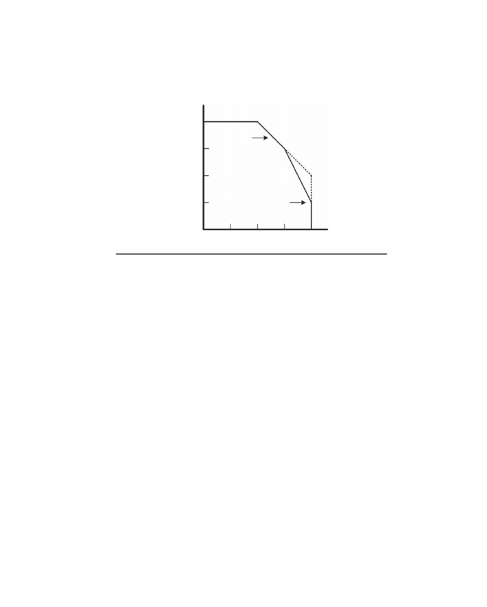
Safe Operating Area
The safe operating area (SOA) for a transistor describes the safe combinations of voltage
and current for the device. This area will be bounded on the X axis by the maximum
operating voltage and on the Y axis by the maximum operating current. The SOA is also
bounded by a line that defines the maximum power dissipation of the device. Such a plot
is shown for a power transistor in Figure 2.4, where voltage and current are plotted on log
scales and the power dissipation limiting line becomes the outermost straight line.
Emitter
ro
Base
Collector
C
cb
r
π
C
π
l
c
= gm × v
be
(gm = 40 × l
c
)
F
igure
2.3 Hybrid pi model.
Copyrighted
Material
24
A u d i o P o w e r A m p l i f i e r B a s i c s
P o w e r A m p l i f i e r B a s i c s
25
Unfortunately, power transistors are not just limited in their safe current-handling
capability by their power dissipation. At higher voltages they are more seriously lim-
ited by a phenomenon called secondary breakdown. This is illustrated by the more steeply
sloped inner line in Figure 2.4.
Although there are many different ways to specify SOA, perhaps the single most
indicative number for audio power amplifier design is the amount of current the tran-
sistor can safely sustain for at least 1 second at some high collector-emitter voltage such
as 100 V. In the absence of secondary breakdown, a 150-W power transistor could sus-
tain a current of 1.5 A at 100 V. In reality, this number may only be 0.5 A, corresponding
to only 50 W of dissipation. Secondary breakdown causes the sustainable power dissi-
pation at high voltages to be less than that at low voltages.
Secondary breakdown results from localized hot spots in the transistor. At higher
voltages the depletion region of the collector-base junction has become larger and the
effective base region has become thinner. Recall that the collector current of a transistor
increases as the junction temperature increases if the base-emitter voltage is held con-
stant. A localized increase in the power transistor’s base-emitter junction temperature
will cause that area to hog more of the total collector current. This causes the local area
to become hotter, conduct even more current, and still become hotter; this leads to a
localized thermal runaway.
SOA is very important in the design of audio amplifier output stages because the
SOA can be exceeded, especially when the amplifier is driving a reactive load. This can
lead to the destruction of the output transistors unless there are safe area protection
circuits in place. There will be a much deeper examination of power transistor SOA in
Chapter 15, including discussion of the higher value of SOA that a transistor can with-
stand for shorter periods of time.
JFETs and MOSFETs
So far nothing has been said about JFET and MOSFET transistors. These will be dis-
cussed in Chapters 7 and 11 where their use in power amplifiers is covered. The short
0.3 A
3 A
10 A
100 W
30 W
V
ce
I
c
1 A
0.1 A
1 V
3 V
10 V
30 V
100 V
F
igure
2.4 Safe operating area.
Copyrighted
Material
24
A u d i o P o w e r A m p l i f i e r B a s i c s
P o w e r A m p l i f i e r B a s i c s
25
version is that they are really not much different than BJTs in many of the characteristics
that have been discussed. Their gate draws essentially no DC current in normal opera-
tion, as they are voltage-controlled devices. Just think of them as transistors with infinite
current gain and about 1/10 the transconductance of BJTs, and you will not be far off.
This is a major simplification, but it is extremely useful for small-signal analysis. In real-
ity, a FET is a square-law device, while the current in a BJT follows an exponential law.
2.2 Circuit Building Blocks
An audio power amplifier is composed of just a few important circuit building blocks put
together in many different combinations. Once each of those building blocks can be under-
stood and analyzed, it is not difficult to do an approximate analysis by inspection of a
complete power amplifier. Knowledge of how these building blocks perform and bring
performance value to the table permits the designer to analyze and synthesize circuits.
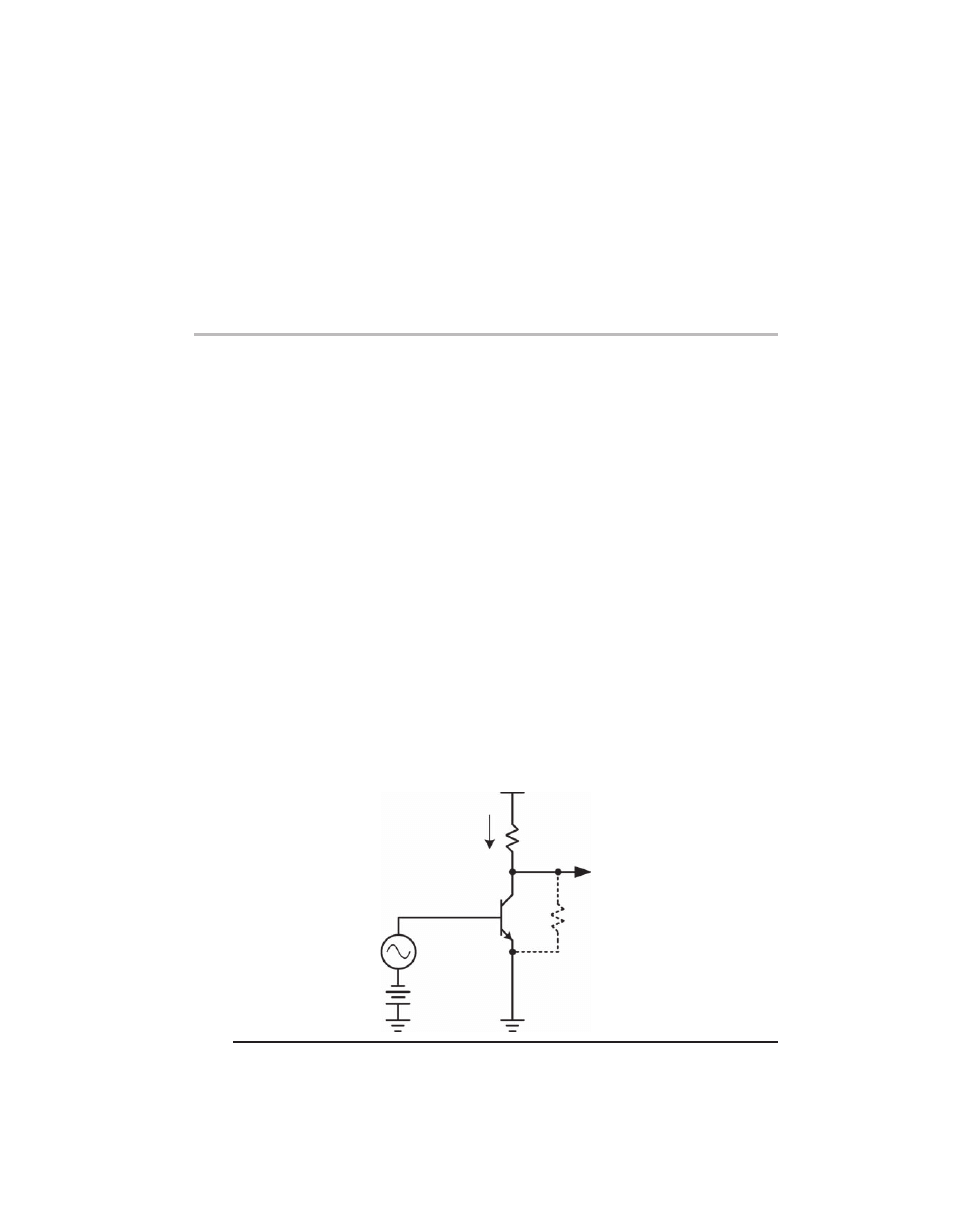
Common-Emitter Stage
The common-emitter (CE) amplifier is possibly the most important circuit building
block, as it provides basic voltage gain. Assume that the transistor’s emitter is at ground
and that a bias current has been established in the transistor. If a small voltage signal is
applied to the base of the transistor, the collector current will vary in accordance with
the base voltage. If a load resistance R
L
is provided in the collector circuit, that resistance
will convert the varying collector current to a voltage. A voltage-in, voltage-out ampli-
fier is the result, and it likely has quite a bit of voltage gain. A simple common emitter
amplifier is shown in Figure 2.5a.
The voltage gain will be approximately equal to the collector load resistance times
the transconductance gm. Recall that the intrinsic emitter resistance re
′ = 1/gm. Thus,
more conveniently, assuming the ideal transistor with intrinsic emitter resistance re
′, the
gain is simply R
L
/re
′.
Consider a transistor biased at 1 mA with a load resistance of 5000
Ω and a supply
voltage of 10 V, as shown in Figure 2.5a. The intrinsic emitter resistance re
′ will be about
26
Ω. The gain will be approximately 5000/26 = 192.
+10 V
Output
Input
signal
Q1
ro
Bias
~0.6 V
re
′ = 1/gm
re
′ = 26 Ω
1 mA
R
L
5000
F
igure
2.5a Common-emitter amplifier.
Copyrighted
Material
26
A u d i o P o w e r A m p l i f i e r B a s i c s
P o w e r A m p l i f i e r B a s i c s
27
This is quite a large value. However, any loading by other circuits that are driven by
the output has been ignored. Such loading will reduce the gain.
The Early effect has also been ignored. It effectively places another resistance ro in
parallel with the 5-k
Ω load resistance. This is illustrated by the dashed resistor drawn
in the figure. As mentioned earlier, ro for a 2N5551 operating at 1 mA and relatively low
collector-emitter voltages will be on the order of 100 k
Ω, so the error introduced by
ignoring the Early effect here will be about 5%.
Because re
′ is a function of collector current, the gain will vary with signal swing
and the gain stage will suffer from some distortion. The gain will be smaller as the cur-
rent swings low and the output voltage swings high. The gain will be larger as the cur-
rent swings high and the output voltage swings low. This results in second harmonic
distortion.
If the input signal swings positive so that the collector current increases to 1.5 mA
and the collector voltage falls to 2.5 V, re
′ will be about 17.3 Ω and the incremental gain
will be 5000/17.3
= 289. If the input signal swings negative so that the collector current
falls to 0.5 mA and the collector voltage rises to 7.5 V, then re
′ will rise to about 52 Ω and
incremental gain will fall to 5000/52
= 96. The incremental gain of this stage has thus
changed by over a factor of 3 when the output signal has swung 5 V peak-to-peak. This
represents a high level of distortion.
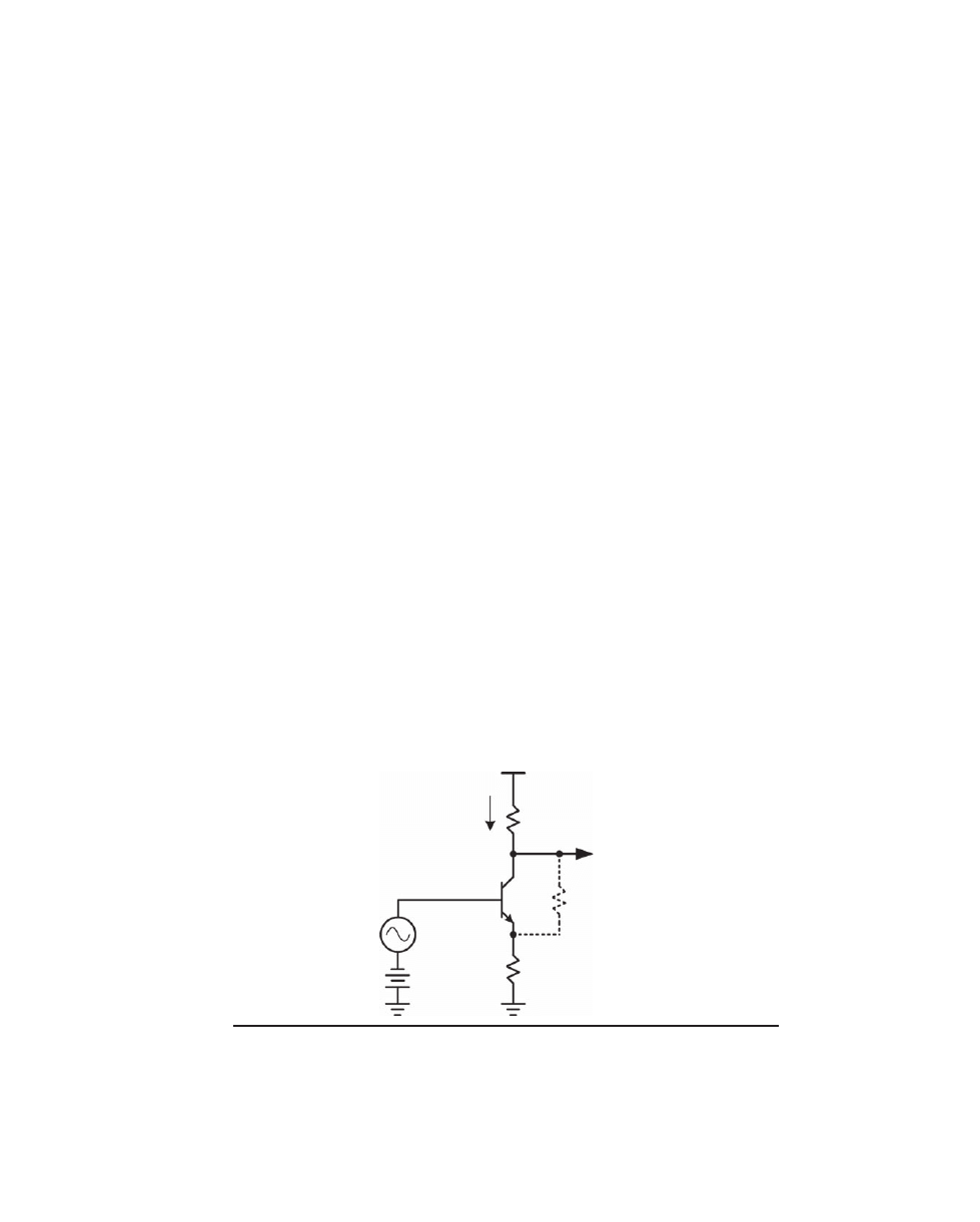
If external emitter resistance is added as shown in Figure 2.5b, then the gain will
simply be the ratio of R
L
to the total emitter circuit resistance consisting of re
′ and the
external emitter resistance R
e
. Since the external emitter resistance does not change with
the signal, the overall gain is stabilized and is more linear. This is called emitter degen-
eration
. It is a form of local negative feedback.
The CE stage in Figure 2.5b is essentially the same as that in 2.5a but with a 234-
Ω
emitter resistor added. This corresponds to 10:1 emitter degeneration because the total
effective resistance in the emitter circuit has been increased by a factor of 10 from 26 to
260
Ω. The nominal gain has also been reduced by a factor of 10 to a value of approxi-
mately 5000/260
= 19.2.
+10 V
Output
Input
signal
Q1
ro
Bias
~0.85 V
1 mA
R
L
5000
R
e
234
F
igure
2.5b CE stage with emitter degeneration.
Copyrighted
Material

26
A u d i o P o w e r A m p l i f i e r B a s i c s
P o w e r A m p l i f i e r B a s i c s
27
Consider once again what happens to the gain when the input signal swings posi-
tive and negative to cause a 5-V peak-to-peak output swing. If the input signal swings
positive so that the collector current increases to 1.5 mA and the collector voltage falls
to 2.5 V, total emitter circuit resistance R
e
will become 17
+ 234 = 251 Ω, and the incre-
mental gain will rise to 5000/251
= 19.9.
If the input signal swings negative so that the collector current falls to 0.5 mA and
the collector voltage rises to 7.5 V, then R
e
will rise to about 234
+ 52 = 287 Ω and incre-
mental gain will fall to 5000/287
= 17.4. The incremental gain of this stage has now
swung over a factor of 1.14:1, or only 14%, when the output signal has swung 5 V
peak to peak. This is indeed a much lower level of distortion than occurred in the un-
degenerated circuit of Figure 2.5a. This illustrates the effect of local negative feedback
without resort to any negative feedback theory.
We thus have, for the CE stage, the approximation
Gain
= R
L
/(re
′ + R
e
)
where R
L
is the net collector load resistance and R
e
is the external emitter resistance. The
emitter degeneration factor is defined as (re
′ + R
e
)/re
′. In this case that factor is 10.
Emitter degeneration also mitigates nonlinearity caused by the Early effect in the
CE stage. As shown by the dotted resistance ro in Figure 2.5b, most of the signal current
flowing in ro is returned to the collector by way of being injected into the emitter. If
100% of the signal current in ro were returned to the collector, the presence of ro would
have no effect on the output resistance of the stage. In reality, some of the signal current
in ro is lost by flowing in the external emitter resistor R
e
instead of through emitter resis-
tance re
′ (some is also lost due to the finite current gain of the transistor). The fraction of
current lost depends on the ratio of re
′ to R
e
, which in turn is a reflection of the amount
of the emitter degeneration. As a rough approximation, the output resistance due to the
Early effect for a degenerated CE stage is
R
out
~ ro
* degeneration factor
If ro is 100 k
Ω and 10:1 emitter degeneration is used as in Fig. 2.5b, then the out-
put resistance of the CE stage due to the Early effect will be on the order of 1 M
Ω.
Bear in mind that this is just a convenient approximation. In practice, the output
resistance of the stage cannot exceed approximately ro times the current gain of the
transistor. It has been assumed that the CE stage here is driven with a voltage source.
If it is driven by a source with significant impedance, the output resistance of the
degenerated CE stage will decrease somewhat from the values predicted above.
That reduction will occur because of the changes in base current that result from the
Early effect.
Bandwidth of the Common-Emitter Stage and Miller Effect
The high-frequency response of a CE stage will be limited if it must drive any load
capacitance. This is no different than when a source resistance drives a shunt capaci-
tance, forming a first-order low-pass filter. A pole is formed at the frequency where the
source resistance and reactance of the shunt capacitance are the same; this causes the
frequency response to be down 3 dB at that frequency. The reactance of a capacitor is
equal to 1/(2
π f C) = 0.159/( f C). The –3 dB frequency f
3
will then be 0.159/(RC).
In Figure 2.5a the output impedance of the CE stage is approximately that of the
5-k
Ω collector load resistance. Suppose the stage is driving a load capacitance of 100 pF.
Copyrighted
Material

28
A u d i o P o w e r A m p l i f i e r B a s i c s
P o w e r A m p l i f i e r B a s i c s
29
The bandwidth will be dictated by the low-pass filter formed by the output impedance
of the stage and the load capacitance. A pole will be formed at
f
3
= 1/(2πR
L
C
L
)
= 0.159/(5 kΩ * 100 pF) = 318 kHz
As an approximation, the collector-base capacitance should also be considered part
of C
L
. The bandwidth of a CE stage is often further limited by the collector-base capaci-
tance of the transistor when the CE stage is fed from a source with significant imped-
ance. The source must supply current to charge and discharge the collector-base
capacitance through the large voltage excursion that exists between the collector and
the base. This phenomenon is called the Miller effect.
Suppose the collector-base capacitance is 5 pF and assume that the CE stage is being
fed from a 5-k
Ω source impedance R
S
. Recall that the voltage gain G of the circuit in
Figure 2.5a was approximately 192. This means that the voltage across C
cb
is 193 times
as large as the input signal (bearing in mind that the input signal is out of phase with
the output signal, adding to the difference). This means that the current flowing through
C
cb
is 193 times as large as the current that would flow through it if it were connected
from the base to ground instead of base to collector. The input circuit thus sees an effec-
tive input capacitance C
in
that is 1
+ G times that of the collector-base capacitance. This
phenomenon is referred to as Miller multiplication of the capacitance. In this case the
effective value of C
in
would be 965 pF.
The base-collector capacitance effectively forms a shunt feedback circuit that ulti-
mately controls the gain of the stage at higher frequencies where the reactance of the
capacitor becomes small. As frequency increases, a higher proportion of the input signal
current must flow to the collector-base capacitance as opposed to the small fixed amount
of signal current required to flow into the base of the transistor. If essentially all of the
input signal current flowed through the collector-base capacitance, the gain of the stage
would simply be the ratio of the capacitive reactance of C
cb
to the source resistance
G
X
R
fC
R
fC R
Ccb
S
S
S
=
=
=
1
2
0 159
(
)( )
.
(
)
π
cb
cb
This represents a value of gain that declines at 6 dB per octave as frequency increases.
This decline will begin at a frequency where the gain calculated here is equal to the low-
frequency gain of the stage. The Miller effect is often used to advantage in providing the
high-frequency roll-off needed to stabilize a negative feedback loop. This is referred to
as Miller compensation.
Differential Amplifier
The differential amplifier is illustrated in Figure 2.6. It is much like a pair of common
emitter amplifiers tied together at the emitters and biased with a common current.
This current is called the tail current. The arrangement is often referred to as a long-tailed
pair
(LTP).
The differential amplifier routes its tail current to the two collectors of Q1 and Q2 in
accordance with the voltage differential across the bases of Q1 and Q2. If the base volt-
ages are equal, then equal currents will flow in the collectors of Q1 and Q2. If the base
of Q1 is more positive than that of Q2, more of the tail current will flow in the collector
of Q1 and less will flow in the collector of Q2. This will result in a larger voltage drop
across the collector load resistor R
L1
and a smaller voltage drop across load resistor R
L2
.
Copyrighted
Material
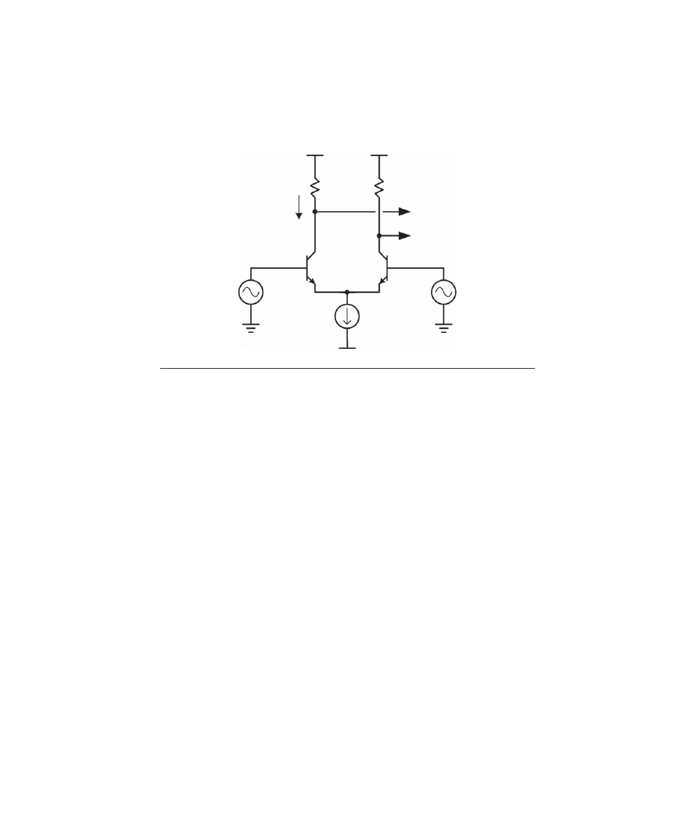
28
A u d i o P o w e r A m p l i f i e r B a s i c s
P o w e r A m p l i f i e r B a s i c s
29
Output A is thus inverted with respect to Input A, while Output B is noninverted with
respect to Input A.
Visualize the intrinsic emitter resistance re
′ present in each emitter leg of Q1 and Q2.
Recall that the value of re
′ is approximately 26 Ω divided by the transistor operating
current in milliamperes. With 1 mA flowing nominally through each of Q1 and Q2, each
can be seen as having an emitter resistance re
′ of 26 Ω. Note that since gm = 1/re′ is depen-
dent on the instantaneous transistor current, the values of gm and re
′ are somewhat signal
dependent, and indeed this represents a nonlinearity that gives rise to distortion.
Having visualized the ideal transistor with emitter resistance re
′, one can now assume
that the idealized internal emitter of each device moves exactly with the base of the tran-
sistor, but with a fixed DC voltage offset equal to V
be
. Now look what happens if the base
of Q1 is 5.2 mV more positive than the base of Q2. The total emitter resistance separating
these two voltage points is 52
Ω, so a current of 5.2 mV/52 Ω = 0.1 mA will flow from the
emitter of Q1 to the emitter of Q2. This means that the collector current of Q1 will be
100
µA more than nominal, and the collector current of Q2 will be 100 µA less than nomi-
nal. The collector currents of Q1 and Q2 are thus 1.1 mA and 0.9 mA, respectively, since
they must sum to the tail current of 2.0 mA (assuming very high
β for the transistors).
This 100-
µA increase in the collector current of Q1 will result in a change of 500 mV
at Output A, due to the collector load resistance of 5000
Ω. A 5.2-mV input change at the
base of Q1 has thus caused a 500-mV change at the collector of Q1, so the stage gain to
Output A in this case is approximately 500/5.2
= 96.2. More significantly, the stage gain
defined this way is just equal numerically to the load resistance of 5000
Ω divided by
the total emitter resistance re
′ = 52 Ω across the emitters.
Had additional external emitter degeneration resistors been included in series with
each emitter, their value would have been added into this calculation. For example, if
48-
Ω emitter degeneration resistors were employed, the gain would then become 5000/
(52
+ 48 + 48 + 52) = 5000/200 = 25. This approach to estimating stage gain is a very
+10 V
+10 V
Input
signal
B
Output A
Output B
Q1
re
′ = 26 re′ = 26
Q2
Input
signal
A
1 mA
2 mA
V
ee
R
L2
5000
R
L1
5000
F
igure
2.6 Differential amplifier.
Copyrighted
Material

30
A u d i o P o w e r A m p l i f i e r B a s i c s
P o w e r A m p l i f i e r B a s i c s
31
important back-of-the-envelope concept in amplifier design. In a typical amplifier
design, one will often start with these approximations and then knowingly account for
some of the deviations from the ideal. This will be evident in the numerous design
analyses to follow.
It was pointed out earlier that the change in transconductance of the transistor as a
function of signal current can be a source of distortion. Consider the situation where a
negative input signal at the base of Q1 causes Q1 to conduct 0.5 mA and Q2 to conduct
1.5 mA. The emitter resistance re
′ of Q1 is now 26/0.5 = 52 Ω. The emitter resistance re′ of
Q2 is now 26/1.5
= 17.3 Ω. The total emitter resistance from emitter to emitter has now
risen from 52
Ω in the case above to 69.3 Ω. This results in a reduced gain of 5000/69.3 =
72.15. This represents a reduction in gain by a factor of 0.75, or about 25%. This is an
important origin of distortion in the LTP. The presumed signal swing that caused the
imbalance of collector currents between Q1 and Q2 resulted in a substantial decrease in
the incremental gain of the stage. More often than not, distortion is indeed the result of a
change in incremental gain as a function of instantaneous signal amplitude.
The gain of an LTP is typically highest in its balanced state and decreases as the
signal goes positive or negative away from the balance point. This symmetrical behav-
ior is in contrast to the asymmetrical behavior of the common-emitter stage, where the
gain increases with signal swing in one direction and decreases with signal swing in the
other direction. To first order, the symmetrical distortion here is third harmonic distor-
tion, while that of the CE stage is predominantly second harmonic distortion.
Notice that the differential input voltage needed to cause the above imbalance in
the LTP is only on the order of 25 mV. This means that it is fairly easy to overload an LTP
that does not incorporate emitter degeneration. This is of great importance in the design
of most power amplifiers that employ an LTP input stage.
Suppose the LTP is pushed to 90% of its output capability. In this case Q1 would be
conducting 0.1 mA and Q2 would be conducting 1.9 mA. The two values of re
′ will be
260
Ω and 14 Ω, for a total of 274 Ω. The gain of the stage is now reduced to 5000/274 =
18.25. The nominal gain of this un-degenerated LTP was about 96.2. The incremental gain
under these large signal conditions is down by about 80%, implying gross distortion.
As in the case of the CE stage, adding emitter degeneration to the LTP will substan-
tially reduce its distortion while also reducing its gain. In summary we have the
approximation
Gain
=
′ +
R
r
L
e
1
2(
)
R
e
where R
L1
is a single-ended collector load resistance and R
e
is the value of external emit-
ter degeneration resistance in each emitter of the differential pair. This gain is for the
case where only a single-ended output is taken from the collector of Q1. If a differential
output is taken from across the collectors of Q1 and Q2, the gain will be doubled. For
convenience, the total emitter-to-emitter resistance in an LTP, including the intrinsic re
′
resistances, will be called R
LTP
. In the example above,
R
LTP
= 2(re′ + R
e
)
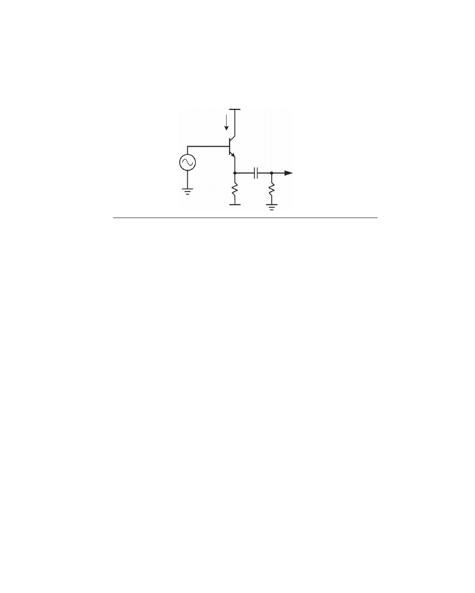
Emitter Follower
The emitter follower (EF) is essentially a unity voltage gain amplifier that provides cur-
rent gain. It is most often used as a buffer stage, permitting the high impedance output
of a CE or LTP stage to drive a heavier load.
Copyrighted
Material
30
A u d i o P o w e r A m p l i f i e r B a s i c s
P o w e r A m p l i f i e r B a s i c s
31
The emitter follower is illustrated in Figure 2.7. It is also called a common collec-
tor (CC) stage because the collector is connected to an AC ground. The output pull-
down resistor R1 establishes a fairly constant operating collector current in Q1. For
illustration, a load resistor R2 is being driven through a coupling capacitor. For AC
signals, the net load resistance R
L
at the emitter of Q1 is the parallel combination of R1
and R2. If re
′ of Q1 is small compared to R
L
, virtually all of the signal voltage applied
to the base of Q1 will appear at the emitter, and the voltage gain of the emitter fol-
lower will be nearly unity.
The signal current in the emitter will be equal to V
out
/R
L
, while the signal current in
the base of Q1 will be this amount divided by the
β of the transistor. It is immediately
apparent that the input impedance seen looking into the base of Q1 is equal to the
impedance of the load multiplied by the current gain of Q1. This is the most important
function of the emitter follower.
As mentioned above, the voltage gain of the emitter follower is nearly unity. Sup-
pose R1 is 9.4 k
Ω and the transistor bias current is 1 mA. The intrinsic emitter resistance
re
′ will then be about 26 Ω. Suppose R2 is 1 kΩ, making net R
L
equal to 904
Ω. The volt-
age gain of the emitter follower is then approximately
G
= R
L
/(R
L
+ re′) = 0.97
At larger voltage swings the instantaneous collector current of Q1 will change with
signal, causing a change in re
′. This will result in a change in incremental gain that cor-
responds to distortion. Suppose the signal current in the emitter is 0.9 mA peak in each
direction, resulting in an output voltage of about 814 mV peak. At the negative peak
swing, emitter current is only 0.1 mA and re
′ has risen to 260 Ω. Incremental gain is
down to about 0.78. At the positive peak swing the emitter current is 1.9 mA and re
′ has
fallen to 13.7
Ω; this results in a voltage gain of 0.985.
Voltage gain has thus changed by about 21% over the voltage swing excursion; this
causes considerable second harmonic distortion. One solution to this is to reduce R1 so
that a greater amount of bias current flows, making re
′ a smaller part of the gain equa-
tion. This of course also reduces net R
L
somewhat. A better solution is to replace R1 with
a constant current source.
The transformation of low-value load impedance to much higher input imped-
ance by the emitter follower is a function of the current gain of the transistor. The
β is
+10 V
–10 V
Output
Q1
C1
re
′ = 26 Ω
Input
signal
1 mA
R1
9.4k
R2
1000
F
igure
2.7 Emitter follower.
Copyrighted
Material

32
A u d i o P o w e r A m p l i f i e r B a s i c s
P o w e r A m p l i f i e r B a s i c s
33
a function of frequency, as dictated by the f
T
of the transistor. This means, for exam-
ple, that a resistive load will be transformed to impedance at the input of the emitter
follower that eventually begins to decrease with frequency as
β
AC
decreases with
frequency. A transistor with a nominal
β of 100 and f
T
of 100 MHz will have an f
β
of
1 MHz. The AC
β of the transistor will begin to drop at 1 MHz. The decreasing input
impedance of the emitter follower thus looks capacitive in nature, and the phase
of the input current will lead the phase of the voltage by an amount approaching
90 degrees.
The impedance transformation works both ways. Suppose we have an emitter fol-
lower that is driven by a source impedance of 1 k
Ω. The low-frequency output imped-
ance of the EF will then be approximately 1 k
Ω divided by β, or about 10 Ω (ignoring re’).
However, the output impedance will begin to rise above 1 MHz where
β begins to fall.
Impedance that increases with frequency is inductive. Thus, Z
out
of an emitter follower
tends to be inductive at high frequencies.
Now consider an emitter follower that is loaded by a capacitance. This can lead to
instability, as we will see. The load impedance presented by the capacitance falls with
increasing frequency. The amount by which this load impedance is multiplied by
β
AC
also falls with frequencies above 1 MHz. This means that the input impedance of the
emitter follower is ultimately falling with the square of frequency. It also means that the
current in the load, already leading the voltage by 90 degrees, will be further trans-
formed by another 90 degrees by the falling transistor current gain with frequency. This
means that the input current of the emitter follower will lead the voltage by an amount
approaching 180 degrees. When current is 180 degrees out of phase with voltage, this
corresponds to a negative resistance. This can lead to instability, since the input imped-
ance of this emitter follower is a frequency-dependent negative resistance under these
conditions. This explains why placing a resistance in series with the base of an emitter
follower will sometimes stabilize it; the positive resistance adds to the negative resis-
tance by an amount that is sufficient to make the net resistance positive.
There is one more aspect of emitter follower behavior that pertains largely to its use
in the output stage of a power amplifier. It was implied above that if an emitter follower
was driven from a very low impedance source that its output impedance would simply
be re
′ of its transistor. This is not quite the whole story. Transistors have finite base resis-
tance. The output impedance of an emitter follower will actually be the value of re
′ plus
the value of the base resistance divided by
β of the transistor. This can be significant in
an output stage. Consider a power transistor operating at 100 mA. Its re
′ will be about
0.26
Ω. Suppose that transistor has a base resistance of 5 Ω and a current gain of 50. The
value of the transformed base resistance will be 0.1
Ω. This is not insignificant com-
pared to the value of re
′ and must be taken into account in some aspects of design. This
can also be said for the emitter resistance of the power transistor, which may range from
0.01 to 0.1
Ω.
The simplicity of the emitter follower, combined with its great ability to buffer a
load, accounts for it being the most common type of circuit used for the output stage
of power amplifiers. An emitter follower will often be used to drive a second emitter
follower to achieve even larger amounts of current gain and buffering. This arrange-
ment is sometimes called a Darlington connection. Such a pair of transistors, each with
a current gain of 50, can increase the impedance seen driving a load by a factor of
2500. Such an output stage driving an 8-
Ω load would present an input impedance of
20,000
Ω.
Copyrighted
Material
32
A u d i o P o w e r A m p l i f i e r B a s i c s
P o w e r A m p l i f i e r B a s i c s
33
Cascode
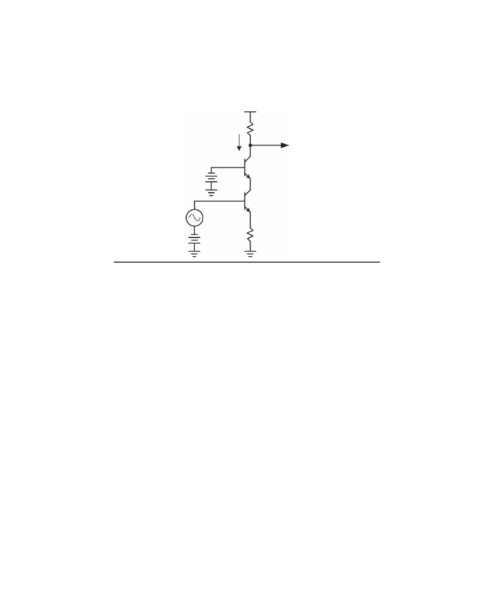
A cascode stage is implemented by Q2 in Figure 2.8. The cascode stage is also called a
common base
stage because the base of its transistor is connected to AC ground. Here the
cascode is being driven at its emitter by a CE stage comprising Q1. The most important
function of a cascode stage is to provide isolation. It provides near-unity current gain,
but can provide very substantial voltage gain. In some ways it is like the dual of an
emitter follower.
A key benefit of the cascode stage is that it largely keeps the collector of the driving
CE stage at a constant potential. It thus isolates the collector of the CE stage from the
large swing of the output signal. This eliminates most of the effect of the collector-base
capacitance of Q2, resulting in wider bandwidth due to suppression of the Miller effect.
Similarly, it mitigates distortion caused by the nonlinear collector-base junction capaci-
tance of the CE stage, since very little voltage swing now appears across the collector-
base junction to modulate its capacitance.
The cascode connection also avoids most of the Early effect in the CE stage by nearly
eliminating signal swing at its collector. A small amount of Early effect remains, how-
ever, because the signal swing at the base of the CE stage modulates the collector-base
voltage slightly.
If the current gain of the cascode transistor is 100, then 99% of the signal current
entering the emitter will flow in the collector. The input-output current gain is thus 0.99.
This current transfer factor from emitter to collector is sometimes referred to as the alpha
of the transistor.
The Early effect resistance ro still exists in the cascode transistor. It is represented as
a resistance ro connected from collector to emitter. Suppose ro is only 10 k
Ω. Is the out-
put impedance of the collector of the cascode 10 k
Ω? No, it is not.
Recall that 99% of the signal current entering the emitter of the cascode re-appears
at the collector. This means that 99% of the current flowing in ro also returns to the
F
igure
2.8 Cascode.
+10 V
Output
Q1
Q2
1 mA
Bias
2 V
Bias
~0.85 V
re
′ = 26 Ω
Input
signal
R
L
5000
R
e
234
Copyrighted
Material
34
A u d i o P o w e r A m p l i f i e r B a s i c s
P o w e r A m p l i f i e r B a s i c s
35
collector. Only the lost 1% of the current in ro results in a change in the net collector
current at the collector terminal. This means that the net effect of ro on the collector
output impedance in the cascode is roughly like that of a 1-M
Ω resistor to ground.
This is why the output impedance of cascode stages is so high even though Early
effect still is present in the cascode transistor.
R
out
= β * ro
ro
VA V
I
c
=
+
ce
ro
≈ VA/I
c
at low V
ce
R
out
= β * VA/I
c
Notice that the product of
β and VA is the Early effect figure of merit mentioned
previously. The output resistance of a cascode is thus the FOM divided by the collector
current.
R
out
= FOM/I
c
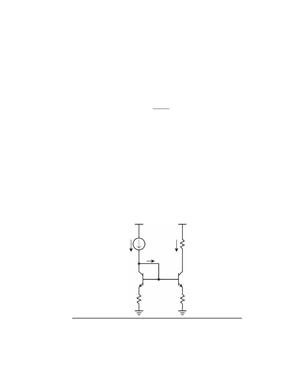
Current Mirror
Figure 2.9a depicts a very useful circuit called a current mirror. If a given amount of
current is sourced into Q1, that same amount of current will be sunk by Q2, assuming
that the emitter degeneration resistors R1 and R2 are equal, that the transistor V
be
drops
are the same, and that losses through base currents can be ignored. The values of R1 and
R2 will often be selected to drop about 100 mV to ensure decent matching in the face of
unmatched transistor V
be
drops, but this is not critical.
F
igure
2.9a Simple current mirror.
+50 V
+50 V
+25 V
2 lb
Q2
Q1
5 mA
~5 mA
R
L
5000
R2
100
R1
100
Copyrighted
Material
34
A u d i o P o w e r A m p l i f i e r B a s i c s
P o w e r A m p l i f i e r B a s i c s
35
If R1 and R2 are made different, a larger or smaller multiple if the input current can
be made to flow in the collector of Q2. In practice, the base currents of Q1 and Q2 cause
a small error in the output current with respect to the input current. In the example
above, if transistor
β is 100, the base current I
b
of each transistor will be 50
µA, causing
a total error of 100
µA, or 2% in the output current.
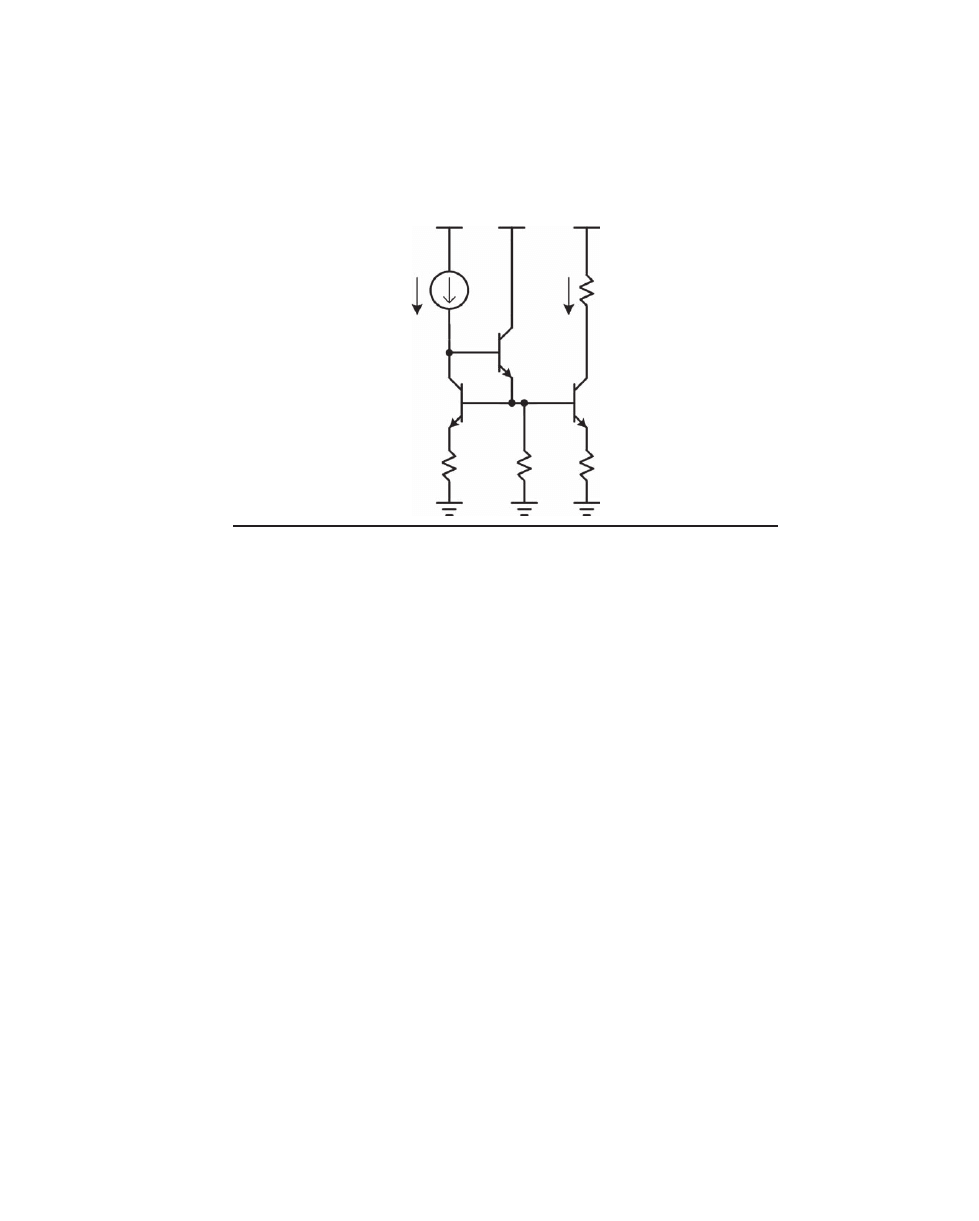
Figure 2.9b shows a variation of the current mirror that minimizes errors due to the
finite current gain of the transistors. Here emitter follower Q3, often called a helper tran-
sistor, provides current gain to minimize that error. Resistor R3 assures that a small
minimum amount of current flows in Q3 even if the current gains of Q1 and Q2 are very
high. Note that the input node of the current mirror now sits one V
be
higher above the
supply rail than in Figure 2.9a.
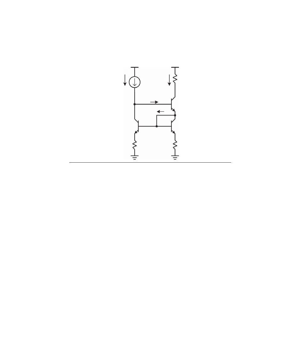
Many other variations of current mirrors exist, such as the Wilson current mirror
shown in Figure 2.9c. The Wilson current mirror includes transistors Q1, Q2, and Q3.
Input current is applied to the base of Q3 and is largely balanced by current flowing in
the collector of Q1. Input current that flows into the base of output transistor Q3 will
turn Q3 on, with its emitter current flowing through Q2 and R2. Q1 and Q2 form a con-
ventional current mirror. The emitter current of Q3 is mirrored and pulled from the
source of input current by Q1.
Any difference between the current of Q1 and the input current is available to drive
the base of Q3. If the input current exceeds the mirrored emitter current of Q3, the base
voltage of Q3 will increase, causing the emitter current of Q3 to increase and self-correct
the situation with feedback action. The equilibrium condition can be seen to be when
the input current and the output current are the same, providing an overall 1:1 current
mirror function.
Notice that in normal operation all three of the transistors operate at essentially the
same current, namely the supplied input current. Ignoring the Early effect, all of the
base currents will be the same if the betas are matched. Assume that each base current
+50 V
+50 V
+50 V
+25 V
Q2
Q1
Q3
5 mA
5 mA
R
L
5000
R1
100
R2
100
R3
10k
F
igure
2.9b Improved current mirror.
Copyrighted
Material
36
A u d i o P o w e r A m p l i f i e r B a s i c s
P o w e r A m p l i f i e r B a s i c s
37
is I
b
and that the collector current in Q1 is equal to I. It can be quickly seen that the input
current must then be I
+ I
b
and that the emitter current of Q3 must be I
+ 2I
b
. It is then
evident that the collector current of Q3, which is the output current, will be I
+ I
b
, which
is the same as the input current. This illustrates the precision of the input-output rela-
tionship when the transistors are matched.
Transistor Q3 acts much like a cascode, and this helps the Wilson current mirror to
achieve high output impedance. Transistors Q1 and Q2 operate at a low collector volt-
age, while output transistor Q3 will normally operate at a higher collector voltage.
Thus, the Early effect will cause the base current of Q3 to be smaller, and this will result
in a slightly higher voltage-dependent output current. This is reflected in the output
resistance of the Wilson current mirror.
Current Sources
Current sources are used in many different ways in a power amplifier, and there are
many different ways to make a current source. The distinguishing feature of a current
source is that it is an element through which a current flows wherein that current is
independent of the voltage across that element. The current source in the tail of the dif-
ferential pair is a good example of its use.
Most current sources are based on the observation that if a known voltage is
impressed across a resistor, a known current will flow. A simple current source is shown
in Figure 2.10a. The voltage divider composed of R2 and R3 places 2.7 V at the base of
Q1. After a V
be
drop of 0.7 V, about 2 V is impressed across emitter resistor R1. If R1 is a
400-
Ω resistor, 5 mA will flow in R1 and very nearly 5 mA will flow in the collector of
Q1. The collector current of Q1 will be largely independent of the voltage at the collec-
tor of Q1, so the circuit behaves as a decent current source. The load resistance R
L
is just
shown for purposes of illustration. The output impedance of the current source itself
(not including the shunting effect of R
L
) will be determined largely by the Early effect in
F
igure
2.9c Wilson current mirror.
+50 V
+50 V
+25 V
lb
Q2
Q3
Q1
5 mA
5 mA
2 lb
R
L
5000
R1
100
R2
100
Copyrighted
Material
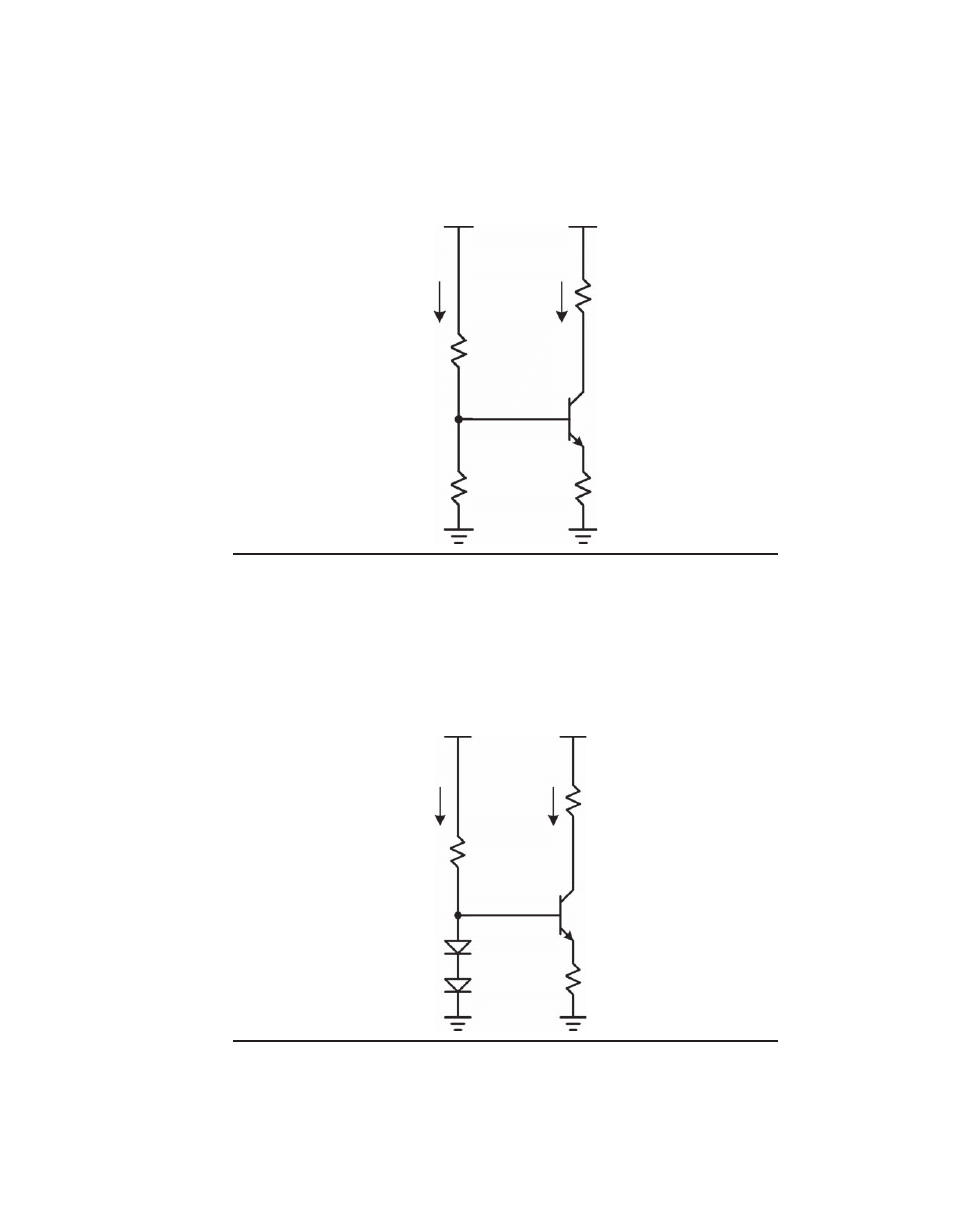
36
A u d i o P o w e r A m p l i f i e r B a s i c s
P o w e r A m p l i f i e r B a s i c s
37
the same way as for the CE stage. The output impedance for this current source is found
by SPICE simulation to be about 290 k
Ω.
In Figure 2.10b, R3 is replaced with a pair of silicon diodes. Here one diode drop is
impressed across R1 to generate the desired current. The circuit employs 1N4148 diodes
biased with the same 0.5 mA used in the voltage divider in the first example. Together
F
igure
2.10a Simple current source.
+50 V
+50 V
+25 V
Q1
2N5551
0.5 mA
~5 mA
R
L
5000
R2
95k
R3
5.4k
R1
400
2.0 V
2.7 V
+50 V
+50 V
+25 V
1N4148
1N4148
Q1
2N5551
0.5 mA
~5 mA
R
L
5000
R2
99k
R1
75
0.38 V
1.11 V
F
igure
2.10b Current source using diodes.
Copyrighted
Material
38
A u d i o P o w e r A m p l i f i e r B a s i c s
P o w e r A m p l i f i e r B a s i c s
39
they drop only about 1.1 V, and about 0.38 V is impressed across the 75-
Ω resistor R1.
The output impedance of this current source is approximately 300 k
Ω, about the same
as the one above.
Turning to Figure 2.10c, R3 is replaced instead with a Green LED, providing a
convenient voltage reference of about 1.8 V, putting about 1.1 V across R1. Once again,
0.5 mA is used to bias the LED. The output impedance of this current source is about
750 k
Ω. It is higher than in the design of Figure 2.10b because there is effectively more
emitter degeneration for Q1 with the larger value of R1.
R3 is replaced with a 6.2-V Zener diode in Figure 2.10d. This puts about 5.5 V across
R1. The output impedance of this current source is about 2 M
Ω, quite a bit higher than
the earlier arrangements due to the larger emitter degeneration for Q1. The price paid
here is that the base of the transistor is fully 6.2 V above the supply rail, reducing head-
room in some applications.
In Figure 2.10e, a current mirror fed from a known supply voltage is used to imple-
ment a current source. Here a 1:1 current mirror is used and 5 mA is supplied from the
known power rail. The output impedance of this current source is about 230 k
Ω. Only
0.25 V is dropped across R1 (corresponding to 10:1 emitter degeneration), and the base
is only 1 V above the rail.
Figure 2.10f illustrates a clever two-transistor feedback circuit that is used to force
one V
be
of voltage drop across R1. It does so by using transistor Q2 to effectively regu-
late the current of Q1. If the current of Q1 is too large, Q2 will be turned on harder and
pull down on the base of Q1, adjusting its current downward appropriately. As in Fig-
ure 2.10a through 2.10d, a 0.5-mA current is supplied to bias the current source. This
current flows through Q2. The output impedance of this current source is an impressive
3 M
Ω. This circuit achieves higher output impedance than the Zener-based version and
yet only requires the base of Q1 to be 1.4 V above the power rail. This circuit can also be
used to place an overcurrent limit on a CE transistor stage implemented with Q1.
+50 V
+50 V
+25 V
Q1
2N5551
0.5 mA
~5 mA
R
L
5000
R2
96k
R1
214
Green
1.08 V
1.81 V
F
igure
2.10c Current source using LED.
Copyrighted
Material
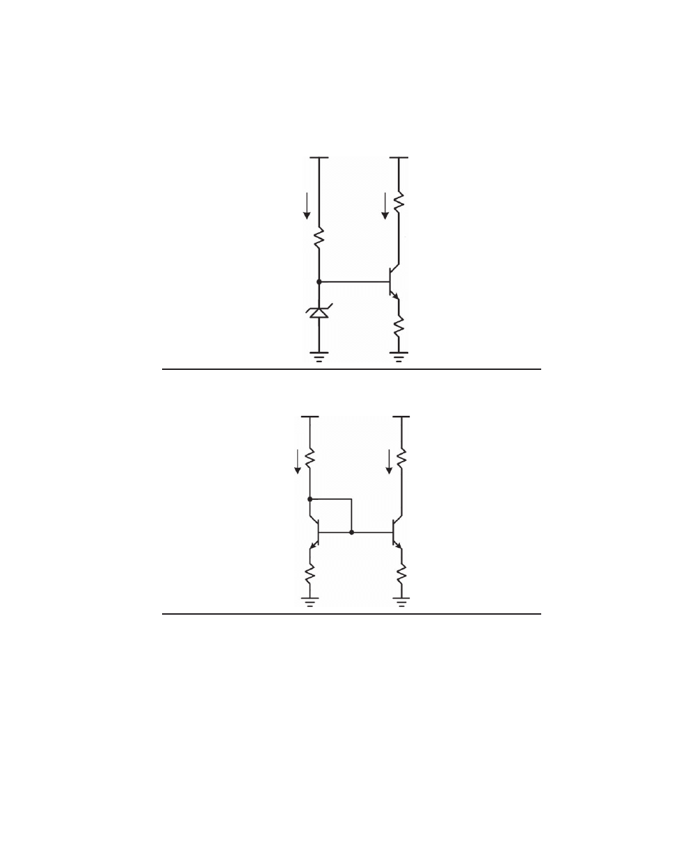
38
A u d i o P o w e r A m p l i f i e r B a s i c s
P o w e r A m p l i f i e r B a s i c s
39
This circuit will work satisfactorily even if less than 0.5 mA (one-tenth of the output
current) is supplied as bias for Q2, but then the output impedance will fall to a lower
value and the “quality” of the current source will suffer somewhat. This happens
because at lower collector current, Q2 has less transconductance and its feedback con-
trol of the current variations in Q1 as a result of the Early effect is less strong. If the bias
current is reduced to 0.1 mA, for example, the output impedance falls to about 1 M
Ω.
+50 V
+50 V
6.2 V
Q1
2N5551
0.5 mA
~5 mA
R
L
5000
+25 V
R2
88k
R1
1.1k
5.5 V
6.2 V
F
igure
2.10d Current source using Zener diode.
+50 V
+50 V
Q1
2N5551
Q2
2N5551
5 mA
~5 mA
R
L
5000
+25 V
R2
9.8k
R1
50
R3
50
0.25 V
0.98 V
F
igure
2.10e Current mirror current source.
Copyrighted
Material
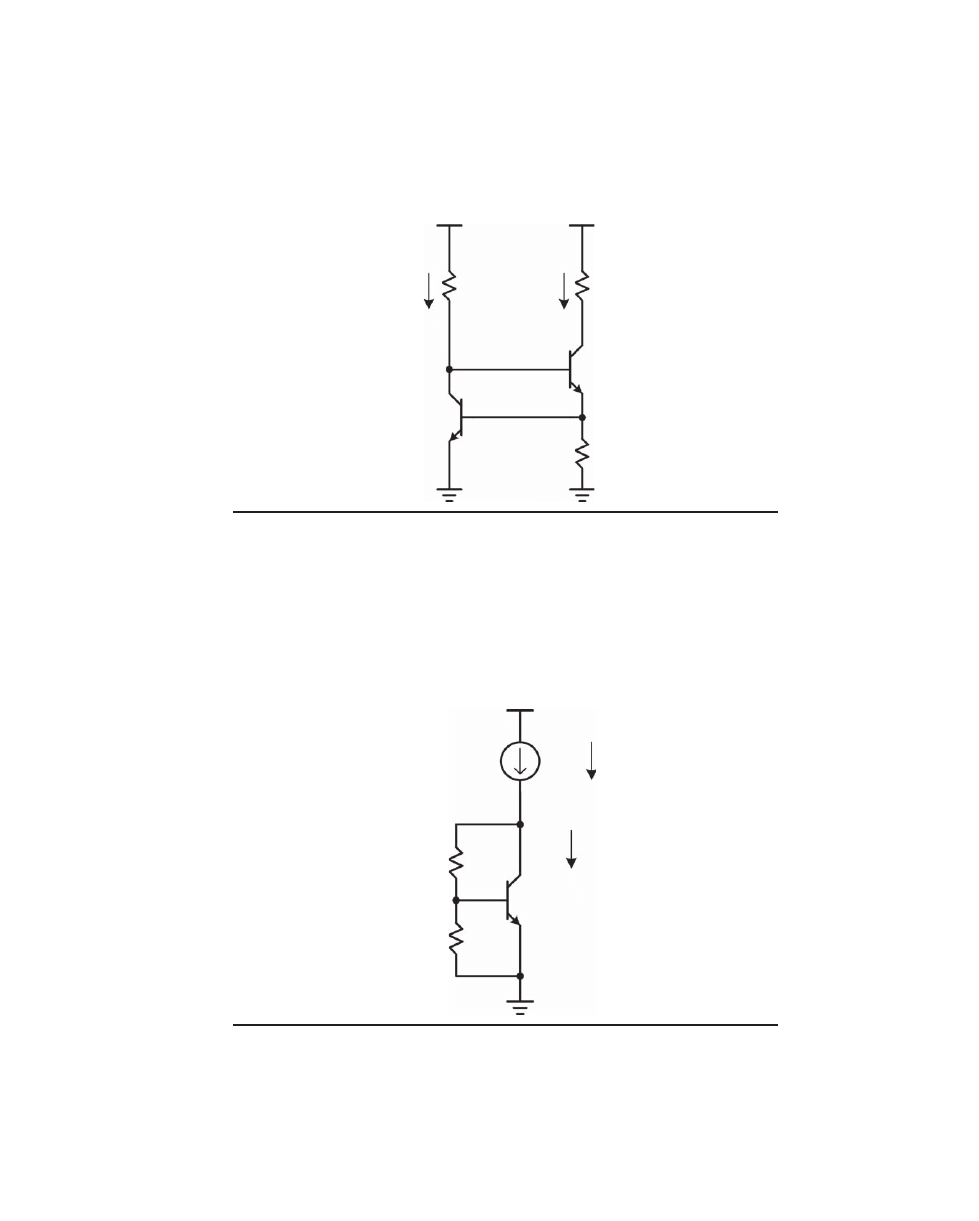
40
A u d i o P o w e r A m p l i f i e r B a s i c s
P o w e r A m p l i f i e r B a s i c s
41
V
be
Multiplier
Figure 2.11 shows what is called a V
be
multiplier
. This circuit is used when a voltage drop
equal to some multiple of V
be
drops is needed. This circuit is most often used as the bias
spreader for power amplifier output stages, partly because its voltage is conveniently
adjustable.
F
igure
2.10f Feedback current source.
+50 V
+50 V
Q1
2N5551
Q2
2N5551
0.5 mA
~5 mA
R
L
5000
+25 V
R2
97k
R1
133
1.4 V
0.67 V
F
igure
2.11 V
be
multiplier.
+50 V
Q1
2N5551
10 mA
~3.0 V
R1
2100
R2
700
0.75 V
9 mA
re
′ = 2.9
Copyrighted
Material

40
A u d i o P o w e r A m p l i f i e r B a s i c s
P o w e r A m p l i f i e r B a s i c s
41
In the circuit shown, the V
be
of Q1 is multiplied by a factor of approximately 4.
Notice that the voltage divider formed by R1 and R2 places about one-fourth of the col-
lector voltage at the base of Q1. Thus, in equilibrium, when the voltage at the collector
is at four V
be
, one V
be
will be at the base, just enough to turn on Q1 by the amount neces-
sary to carry the current supplied. This is simply a shunt feedback circuit. In this
arrangement, about 1 mA flows through the resistive divider while about 9 mA flows
through Q1.
When the V
be
multiplier is used as a bias spreader, R2 will be made adjustable with
a trim pot. As R2 is made smaller the amount of bias voltage is increased. Notice that if
for some reason R2 fails open, the voltage across the V
be
multiplier falls to about one V
be
,
failing in the safe direction.
In practice the V
be
multiplication ratio will be a bit greater than 4 due to the base
current required by Q1 as a result of its finite current gain. The extra drop caused across
R1 by the base current will slightly increase the collector voltage at equilibrium, making
the apparent multiplier factor slightly larger than 4.
The impedance of the V
be
multiplier is about 4 re
′ for Q1. At 9 mA, re′ is 2.9 Ω, so
ideally the impedance of the multiplier would be about 11.6
Ω. In practice, SPICE simu-
lation shows it to be about 25
Ω. This larger value is mainly a result of the finite current
gain of Q1.
The impedance of the V
be
multiplier rises at high frequencies. This is a result of
the fact that the impedance is established by a negative feedback process. The
amount of feedback decreases at high frequencies and the impedance-reducing
effect is lessened. The impedance of the V
be
multiplier in Figure 2.11 is up by 3 dB at
about 2.3 MHz and doubles for every octave increase in frequency from there. It is
thus inductive. For this reason, the V
be
multiplier is often shunted by a capacitor of
0.1 to 10
µF. A shunt capacitance of as little as 0.1 µF eliminates the increase in imped-
ance at high frequencies.
2.3 Amplifier Design Analysis
Here we apply the understanding of transistors and circuit building blocks to analyze
the basic power amplifier. Having accomplished this, we will be well armed to explore,
evolve, and analyze the amplifier design steps that will be taken to achieve high perfor-
mance in the next chapter.
Figure 2.12 is a schematic of a basic 50-W power amplifier that includes the three
stages that appear in most solid-state power amplifiers.
• Differentialinputstage(IPS)comprisingQ1
–
Q3
• VoltageAmplificationStage(VAS)comprisingQ4,Q6,andQ7
• Outputstage(OPS)comprisingQ8
–
Q11
The design also includes a bias spreader implemented with Q5 connected as a V
be
multiplier. Some details like coupling capacitors, input networks, and output networks
have been left out for simplicity.
The amplifier of Figure 2.12 will be described in simple terms, so that those who are
less familiar with circuit design will quickly come to understand its behavior. Those
who are already familiar with these concepts can relax and skim through this section.
Copyrighted
Material
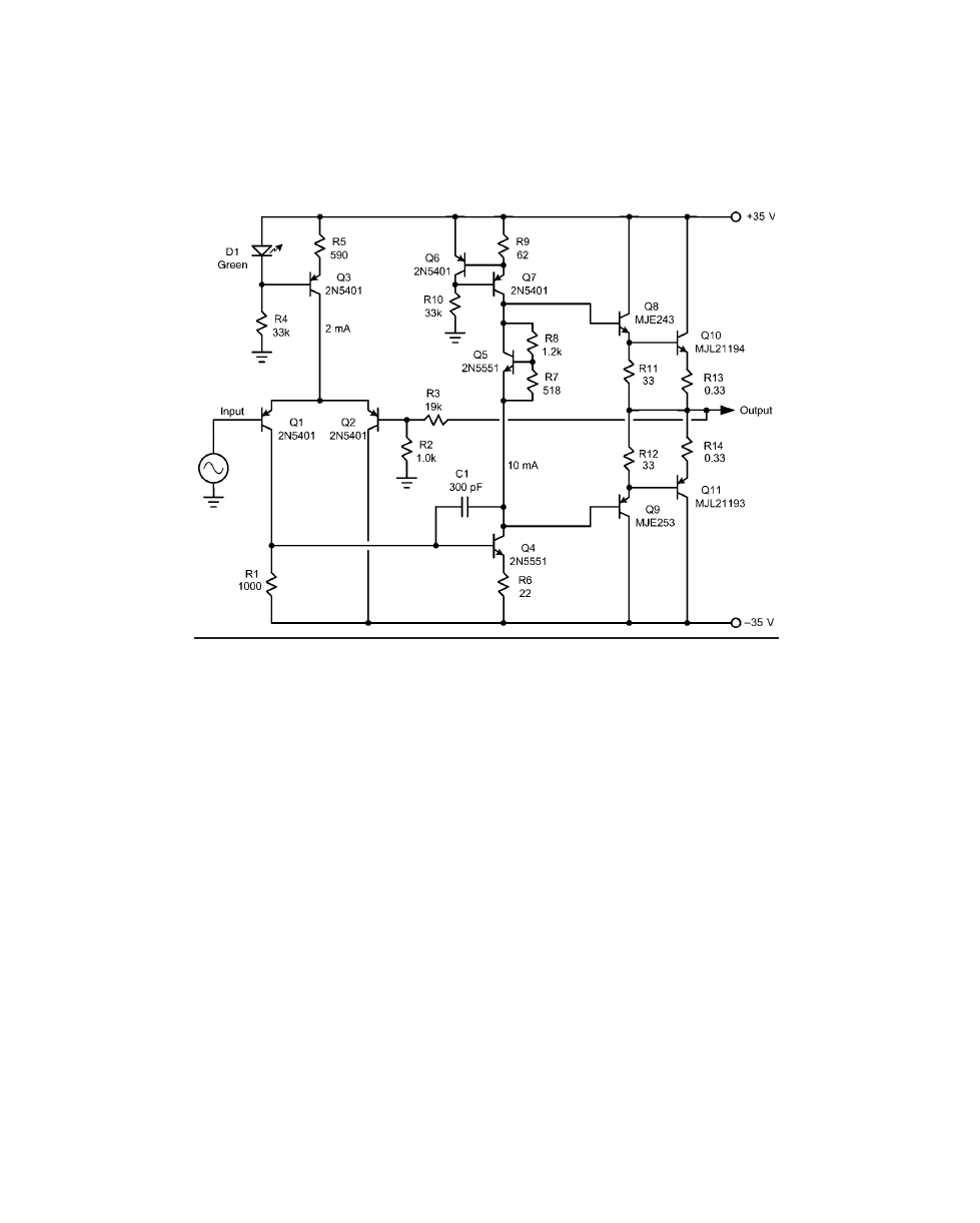
42
A u d i o P o w e r A m p l i f i e r B a s i c s
P o w e r A m p l i f i e r B a s i c s
43
Basic Operation
This simple design is a more detailed version of the basic amplifier design illustrated in
Figure 1.5. As shown, it is a DC-coupled design, so that even DC changes at the input
will be amplified and presented at the output.
Input Stage
The input signal is applied to the input differential pair at the base of Q1. A fraction of
the output signal is coupled via the negative feedback path to the other differential
input at the base of Q2. Transistor Q3 implements a 2-mA current source that provides
tail current to the differential pair. This input arrangement is often called a Long-Tailed
Pair
(LTP).
Feedback resistors R2 and R3 implement a voltage divider that feeds back 1/20 of
the output signal to the input stage. The forward path gain of the amplifier in the
absence of negative feedback is called the open-loop gain (A
ol
)
. If the open-loop gain is
large, then the error signal across the bases of Q1 and Q2 need only be very small to
produce the desired output. If the signals at the bases of Q1 and Q2 are nearly equal,
then the output of the amplifier must be 20 times that of the input, resulting in a closed-
loop gain (A
cl
)
of 20. This is just a very simplified explanation of the negative feedback
process.
F
igure
2.12 A basic 50-W power amplifier.
Copyrighted
Material
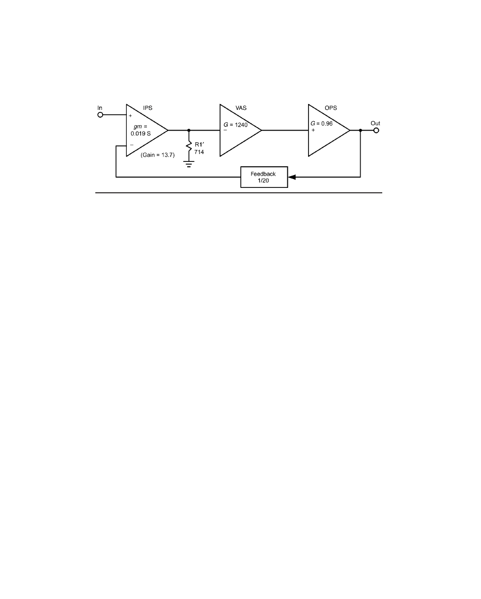
42
A u d i o P o w e r A m p l i f i e r B a s i c s
P o w e r A m p l i f i e r B a s i c s
43
The approximate low-frequency gain of the input stage is the ratio of the net col-
lector load resistance divided by the total emitter-to-emitter resistance R
LTP
(which
includes the intrinsic emitter resistance re
′ of Q1 and Q2). With each transistor biased
at 1 mA, the intrinsic emitter resistance re
′ is about 26 Ω each, so the total emitter-to-
emitter resistance is 52
Ω. If we assume that the β of the following VAS transistor Q4 is
infinity, the net IPS collector load resistance is just that of R1. The DC gain of the IPS is
then 1000/52
= 19. In practice the finite β of Q4 reduces this to about 13.7 if we assume
that the
β of Q4 is 100.
IPS gain
≈ 13.7
The amplifier at low frequencies is illustrated in Figure 2.13 where the input stage
is shown as a block of transconductance with gm
= 1/52 Ω = 0.019 S. The R
1
′ load of
714
Ω on the IPS is just the parallel combination of R1 and the estimated input imped-
ance of the VAS.
The VAS
The VAS is formed by common-emitter transistor Q4 loaded by the 10-mA current
source formed by Q6 and Q7. Recall from the discussion of current sources above that
Q6 forces one V
be
(here about 620 mV) across 62-
Ω resistor R9
;
this produces the desired
current flow.
Emitter degeneration has been applied to Q4 in the form of R6. At 10 mA, re
′ of Q4
is about 2.6
Ω. The 22-Ω resistance of R6 therefore increases the total effective emitter
circuit resistance to about 25
Ω, or by a factor of nearly 10. This corresponds to 10:1
emitter degeneration. The emitter degeneration makes the VAS stage more linear in its
operation.
If the
β of Q4 is assumed to be 100, the input impedance of the VAS will be about
100
* 25 Ω = 2500 Ω. This impedance is in parallel with R1, making the actual load on
the first stage approximately 714
Ω. The voltage gain of the input stage is therefore
close to 13.7. The loading of Q4 thus plays a substantial role in determining the first-
stage gain. It would play a far greater role if Q4 were not degenerated by R6. In that
case the impedance seen looking into the base of Q4 would be only about 260
Ω (β =
100 times re
′ = 2.6 Ω).
The low-frequency gain of the VAS will be set by the ratio of its collector load
impedance to its total effective emitter resistance of about 25
Ω. The VAS collector load
F
igure
2.13 Amplifier gain at low frequencies.
Copyrighted
Material

44
A u d i o P o w e r A m p l i f i e r B a s i c s
P o w e r A m p l i f i e r B a s i c s
45
impedance in this simple design is dominated by the loading of the output stage, since
the output impedance of the current source is quite high.
The output stage is a complementary Darlington arrangement, buffering the loud-
speaker load impedance as seen by the VAS collector circuit. The amount of buffering
depends on the current gain of the driver and output transistors. Throughout these
discussions it will be assumed that small-signal transistors have current gain of 100 and
power transistors have current gain of 50. If the driver and output transistor current
gains are assumed to be 100 and 50 respectively, the buffering factor will be the product
of these, or about 5000. If the load impedance at the output is assumed to be 8
Ω, this
will appear as a load impedance of 40,000
Ω to the VAS collector circuit. The gain of the
VAS is thus on the order of 40,000/25
= 1600.
In the discussion on the Early effect in Section 2.1 it was shown that a common-
emitter stage like the VAS used here (10-mA bias, 10:1 emitter degeneration) has an
intrinsic output impedance of about 135 k
Ω. Recall that the output resistance ro for a
transistor is
ro
VA V
I
c
=
+
ce
and that R
out
for a common-emitter stage with degeneration is approximated by
R
out
= ro * degeneration factor
The Early voltage for the 2N5551 is about 100 V. At a collector current of 10 mA and
a V
ce
of 35 V, ro for the 2N5551 will be about 13.5 k
Ω. With 10:1 degeneration, R
out
of the
CE stage will be about 135 k
Ω, or about 3.4 times that of the load imposed by the output
stage.
The net collector load impedance is the parallel combination of the 135-k
Ω Early
effect resistance and the 40-k
Ω effective external load resistance, or 31 kΩ. The output
resistance of the current source has been ignored because it is much higher. The esti-
mated voltage gain of the VAS equal to 31 k
Ω/25 = 1240.
VAS gain
≈ 1240
This VAS voltage gain of 1240 is shown in Figure 2.13.
Open-Loop Gain
If the voltage gain of the output stage is approximately unity, the forward gain of the
amplifier (without considering negative feedback) is the product of the input stage gain
and the VAS gain, or about 13.7
* 1240 ≈ 17,000. Recall that we refer to this as the open-
loop gain A
ol
. In reality the gain of the output stage is about 0.96 when driving an 8-
Ω
load, so the open-loop gain is a bit less.
Open-loop gain
≈ 16,300
Because the feedback network attenuates the signal by a factor of 20, the gain around
the feedback loop, or loop gain, is about 816. This corresponds to about 58 dB of nega-
tive feedback (NFB) at low frequencies.
Loop gain
≈ 816
NFB
≈ 20 log(816) ≈ 58 dB
Copyrighted
Material
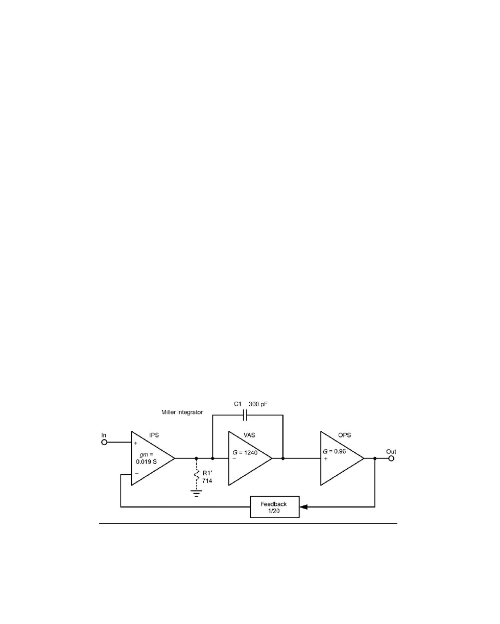
44
A u d i o P o w e r A m p l i f i e r B a s i c s
P o w e r A m p l i f i e r B a s i c s
45
If the amplifier is producing 20 V at its output, the error signal across the bases of
Q1 and Q2 needs only to be 20/16,300
= 1.2 mV. Earlier it was asserted that the closed-
loop gain would be approximately 20 on the basis of the feedback network attenuating
the output by a factor of 20 and the required differential input to the amplifier being
small. Because the input only needs to be 1.2 mV (compared to the input signal level of
1 V), it is apparent that this is a very good approximation.
Miller Feedback Compensation
Capacitor C1 is the so-called Miller compensation capacitor C
M
. It plays a critical role in
stabilizing the global negative feedback loop around the amplifier. It does this by roll-
ing off the high-frequency gain of the amplifier so that the gain around the feedback
loop falls below unity before enough phase lag builds up to cause instability. This will
be discussed in much more detail in Chapter 4.
The effect of Miller compensation capacitor C1 on the open-loop gain is illustrated
in Figure 2.14. Here the topology of the amplifier has effectively transitioned from that
of Figure 2.13 to that of Figure 2.14 as the analysis has gone from low frequencies to
high frequencies. In Figure 2.14 the combined gain of the input stage and the VAS is
equal to the product of the transconductance of the IPS and the impedance of C1. At
high frequencies the gain is dominated by C1 rather than by R1
′.
The capacitor controls the high-frequency AC gain of the VAS by forming a shunt
feedback loop around the VAS transistor. At higher frequencies, virtually all of the signal
current from the LTP input stage flows through C1. This creates a voltage drop across C1
that becomes the output voltage of the VAS. At this point the VAS is acting like a so-
called Miller integrator, where the output voltage is the integral of the input current.
While at low frequencies the gain of the combined input stage and VAS is set by the
product of the individual voltage gains of those two stages, at higher frequencies that
combined gain is set by the ratio of the impedance of C1 to the total emitter resistance
(1/gm) in the LTP. That is because the signal current from the input stage is inversely
proportional to the total LTP emitter resistance R
LTP
. Since the impedance of C1 is
inversely related to frequency, the gain set by it will decrease at 6 dB per octave as fre-
quency increases. The frequency at which the AC gain based on this calculation becomes
F
igure
2.14 Amplifier gain at high frequencies.
Copyrighted
Material
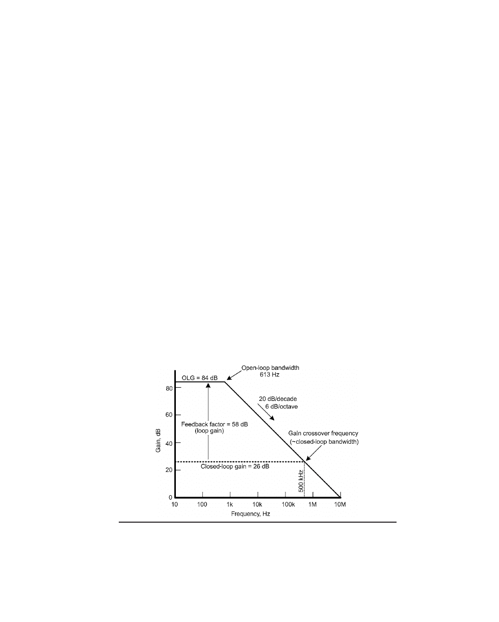
46
A u d i o P o w e r A m p l i f i e r B a s i c s
P o w e r A m p l i f i e r B a s i c s
47
smaller than the DC gain is where the roll-off of the amplifier’s open-loop frequency
response begins.
Assume for the moment an operating frequency of 20 kHz. At this frequency the
reactance of C1 is 1/(2
π * 20 kHz * 300 pF) = 26,500 Ω. If all of the signal current pro-
vided by the LTP passes through C1, then the gain of the combined input and VAS stage
at this frequency is 26,500/52
= 510. This is considerably less than the low-frequency
open-loop gain of 17,000. This means that the capacitor is dominating the gain at this
frequency. This further supports the validity of the assumption that essentially all sig-
nal current from the LTP flows through the capacitor at this frequency.
The frequency where the gain around the negative feedback loop becomes unity is
called the gain crossover frequency f
c
, or simply the unity-gain frequency. This is illustrated
by Figure 2.15, which is called a Bode plot. It shows the various gains of the amplifier in
an idealized form with straight lines.
The open-loop gain starts out at 84 dB at low frequencies and begins to fall off at
20 dB per decade starting at about 613 Hz. This frequency corresponds to the open-loop
bandwidth and is the frequency where the behavior of the amplifier transitions from
that of Figure 2.13 to that of Figure 2.14.
The closed-loop gain of 20, corresponding to 26 dB, is shown as the horizontal dot-
ted line. Where it intersects the falling open-loop gain line is the gain crossover frequency.
This also corresponds approximately to the actual closed-loop bandwidth of the ampli-
fier. Here, that crossing occurs at 500 kHz. The distance between the closed-loop gain
line and the open-loop gain curve represents the amount of negative feedback, often
called loop gain because it is the gain around the feedback loop.
The gain crossover frequency f
c
is chosen to be low enough to assure adequate feed-
back loop stability. There is a trade-off between stability and distortion here. Making the
gain crossover frequency higher results in more negative feedback at high frequencies
F
igure
2.15 Bode plot of the amplifier.
Copyrighted
Material

46
A u d i o P o w e r A m p l i f i e r B a s i c s
P o w e r A m p l i f i e r B a s i c s
47
and less high-frequency distortion. Making the gain crossover frequency too high jeop-
ardizes loop stability. For this amplifier f
c
has been chosen to be 500 kHz as a reasonable
compromise between distortion reduction and stability.
The high-frequency open-loop gain of this simple amplifier is the ratio of Miller
capacitor reactance to IPS total emitter resistance R
LTP
. The closed-loop gain A
cl
is the
same as the attenuation ratio in the feedback path. The Miller capacitance needed to
establish a gain crossover frequency f
c
is then simply
C
Miller
= 1/(2π f
c
*
R
LTP
*
A
cl
)
= 0.159/(500 kHz * 52 Ω * 20) = 306 pF
If instead we define C
Miller
in terms of the transconductance of the IPS, gm
LTP
, we have
C
Miller
= gm
LTP
/(2
π f
c
*
A
cl
)
This shows clearly that increasing the gm of the LTP requires a corresponding increase
in C
Miller
to maintain the same f
c
.
The gain crossover frequency for most audio power amplifiers usually lies between
200 kHz and 2 MHz. If the open-loop gain falls off at 6 dB per octave (as it does with
simple Miller compensation), this corresponds to 20 dB per decade. It can then be seen
that an amplifier with a gain crossover frequency of 200 kHz will have about 20 dB of
negative feedback at 20 kHz. An amplifier with a 2-MHz gain crossover frequency will
have about 40 dB of negative feedback at 20 kHz.
The Output Stage
The output stage is a class AB complementary Darlington arrangement consisting of
emitter follower drivers Q8 and Q9 followed by output devices Q10 and Q11. Emitter
resistors R11 and R12 set the idle current of the drivers at about 20 mA. The output stage
emitter resistors R13 and R14 provide thermal bias stability and also play a role in con-
trolling crossover distortion. These resistors will also be referred to as R
E
. The output
stage provides a voltage gain of slightly less than unity. Its main role is to buffer the out-
put of the VAS with a large current gain. If driver transistor betas are assumed to be 100 and
output transistor betas are assumed to be 50, the combined current gain of the output
stage is 5000. When driving the 8-
Ω output load as shown, the load impedance seen by
the VAS looking into the output stage will be about 40,000
Ω.
On positive half-cycles of the signal, Q8 and Q10 conduct current and transport the
signal to the output node by sourcing current into the load. On negative half-cycles, Q9
and Q11 conduct current and transport the signal to the output node by sinking current
from the load. When there is no signal, a small idle bias current of approximately 100 mA
flows from the top NPN output transistor through the bottom PNP output transistor. A
key observation is that the signal takes a different path through the output stage on
positive and negative half-cycles. If the voltage or current gains of the top and bottom
parts of the output stage are different, distortion will result. Moreover, the “splice point”
where the signal current passes through zero and crosses from one path to the other can
be tricky, and this can lead to so-called crossover distortion.
The voltage gain of the output stage is determined by the voltage divider formed by
the output stage emitter follower output impedance and the loudspeaker load imped-
ance. The output impedance of each half of the output stage is approximately equal to
re
′ plus R
E
. This is illustrated in Figure 2.16.
Copyrighted
Material
48
A u d i o P o w e r A m p l i f i e r B a s i c s
P o w e r A m p l i f i e r B a s i c s
49
Since the two halves of the output stage act in parallel when they are both active at
idle and under small-signal conditions, the net output impedance will be about half
that of each side.
Z
out(small signal)
≈ (re′
idle
+ R
E
)/2
If the output stage is biased at 100 mA, then re
′ of each output transistor will be
about 0.26
Ω. The summed resistance for each side will then be 0.26 + 0.33 = 0.59 Ω. Both
output halves being in parallel will then result in an output impedance of about 0.3
Ω.
Because voltage gain is being calculated, these figures assume that the output stage is
being driven by a voltage source. If the load impedance is 8
Ω, then the voltage gain of
the output stage will be 8/(8
+ 0.3) = 0.96, as shown in Figures. 2.13 and 2.14. If instead
the load impedance is 4
Ω, the gain of the output stage will fall to 0.93. The voltage
divider action governing the output stage gain is illustrated in Figure 2.17.
Bear in mind that the small-signal gain of the output stage has been calculated at its
quiescent bias current. The value of re
′ for each of the output transistors will change as
transistor currents increase or decrease, giving rise to complex changes in the output
stage gain. Moreover, at larger signal swings only one half of the output stage is active.
This means that the output impedance under those conditions will be approximately
+35 V
–35 V
Bias
100 mA
Q10
Q11
R
E
0.33
R
E
0.33
Input
Output
re
′
0.26
re
′
0.26
F
igure
2.16 Push-pull output stage.
Output stage
Voltage divider
+1
Source
Function of I
LOAD
z
out
0.3
Ω
z
LOAD
8
Ω
I
LOAD
F
igure
2.17 Amplifier output stage gain.
Copyrighted
Material
48
A u d i o P o w e r A m p l i f i e r B a s i c s
P o w e r A m p l i f i e r B a s i c s
49
re
′ + R
E
rather than half that amount. These changes in incremental output stage gain as
a function of output signal current cause what is called static crossover distortion.
Z
out(large signal)
≈ re′
high current
+ R
E
≈ R
E
At high current, re
′ becomes very small. At 1 A, re′ is just 0.026 Ω, much smaller than
a typical value of R
E
. At 10 A, re
′ is theoretically just 0.0026 Ω. That is why Z
out(large signal)
≈
R
E
. If R
E
is chosen so that
R
E
= re′
idle
then
Z
out(large signal)
≈ Z
out(small signal)
≈ R
E
and crossover distortion is minimized by making the large-signal and small-signal
output stage gains approximately equal [2]. This is only a compromise solution and
does not eliminate static crossover distortion because the equality does not hold at
intermediate values of output current as the signal passes through the crossover
region. This variation in output stage gain as a function of output current is illus-
trated in Figure 2.18.
Output Stage Bias Current
The idle bias current of the output stage plays a critical role in controlling crossover
distortion. It is important that the right amount of bias current flows through the out-
put stage, from top to bottom, when the output is not delivering any current to the
load. Notice that together the two driver and two output transistors require at least
four V
be
voltage drops from the base of Q8 to the base of Q9 to begin to turn on. Any
additional drop across the output emitter resistors will increase the needed bias spread-
ing voltage.
F
igure
2.18 Output stage gain versus output current.
Copyrighted
Material

50
A u d i o P o w e r A m p l i f i e r B a s i c s
P o w e r A m p l i f i e r B a s i c s
51
The optimum class AB idle bias for a conventional output stage like this is that
amount of current that produces a voltage drop of approximately 26 mV across each of
the output emitter resistors [2]. Recall that
re
′ = V
T
/I
c
= 26 mV/I
c
Then
I
c
= 26 mV/re′ = 26 mV/R
E
and
V
RE
= I
c
* R
E
= 26 mV
This amount of bias current makes re
′ of the output transistor equal to the resistance
of its associated emitter resistor. With 0.33-
Ω emitter resistors, this corresponds to about
79 mA. In the example design here I have chosen to overbias the output stage slightly
to a current of 100 mA. This means that small-signal gain will be slightly larger than
large-signal gain in this case. This is evident in Figure 2.18.
There is a caveat to the assertion that the optimum bias point occurs when 26 mV is
dropped across each output emitter resistor. Recall from Section 2.1 that the actual out-
put impedance of an emitter follower is slightly greater than re
′. The additional resis-
tance results from physical base and emitter resistances inside the transistor. This
additional resistive component acts as an extension of the external emitter resistor R
E
.
This means that the optimum voltage drop across the external emitter resistor will be
somewhat less than 26 mV.
The required bias voltage for the output stage is developed across the bias spreader
comprising a V
be
multiplier built around Q5. In practice R7 is adjusted to set the output
stage bias current to the desired value.
The objective of the bias spreader design is temperature stability of the bias point of
the output stage. The temperature coefficient of the voltage produced by the V
be
multi-
plier should match approximately that of the base-emitter junction voltages of the
driver and output transistors. Since the V
be
of a transistor decreases by about 2.2 mV/
°C,
it is important for thermal bias stability that these junction drops track one another
reasonably. The output transistors will usually heat up the most. Because they are
mounted on a heat sink, Q5 should also be mounted on the heat sink so that it is exposed
to the same approximate temperature. This approach is only an approximation, because
the drivers are often not mounted on the heat sink and because the temperature of the
heat sink changes more slowly in time than that of the power transistor junctions.
Performance Limitations of the Simple Amplifier
The basic amplifier of Figure 2.12 has a decent low-frequency open-loop gain of about
16,300, or about 84 dB. With a closed-loop gain of 20 (26 dB) it has a feedback factor of
about 816, corresponding to about 58 dB of negative feedback. However, its open-loop
gain has not been made very linear and it is very vulnerable to
β variations with signal
in the output stage.
The feedback compensation was set to obtain a moderate negative feedback gain
crossover frequency f
c
of 500 kHz. This will typically result in a closed-loop 3-dB band-
width of about 500 kHz. Selection of f
c
= 500 kHz is what governed the choice of C1 at
300 pF. With f
c
= 500 kHz and the assumed 6 dB per octave roll-off, the amount of negative
Copyrighted
Material

50
A u d i o P o w e r A m p l i f i e r B a s i c s
P o w e r A m p l i f i e r B a s i c s
51
feedback at 20 kHz is about 500 kHz/20 kHz
= 25, corresponding to 28 dB. This means
that there will be less distortion correction at 20 kHz than at low frequencies.
Notice that the input stage can never deliver more than ±1 mA with respect to its
nominal bias point. If all of this 1-mA swing goes into charging or discharging C1, the
maximum voltage rate of change across C1 will be 1 mA/300 pF
= 3.3 V/µs. This is very
inadequate for virtually any power amplifier and will likely result in high frequency
distortion often referred to as slewing-induced distortion (SID) or transient intermodulation
distortion (TIM)
[3, 4, 5]. Even with a demanded voltage rate of change well below the
slew rate limit of 3.3 V/
µs, the un-degenerated input differential stage will become
nonlinear and produce high-frequency distortion.
These limitations will all be addressed in the next chapter as the design is evolved
to a high-performance architecture.
References
1. Massobrio, Giuseppe, and Paolo Antognetti, Semiconductor Device Modeling with
SPICE,
2d ed., New York, McGraw-Hill, 1993.
2. Oliver, B. M., “Distortion in Complementary Pair Class B Amplifiers,” Hewlett Packard
Journal
, pp. 11–16, February, 1971.
3. Otala, M., “Transient Distortion in Transistorized Audio Power Amplifiers,” IEEE
Transactions on Audio and Electro-acoustics
, Vol. AU-18, pp. 234–239, September, 1970.
4. Jung, W.G., M. L. Stephens, and C.C. Todd, “Slewing Induced Distortion and Its Effect
on Audio Amplifier Performance–With Correlated Measurement Listening Results,”
AES preprint No. 1252 presented at the 57th AES Convention, Los Angeles, May, 1977.
5. Cordell, R. R., “Another View of TIM,” Audio, February & March, 1980.
Copyrighted
Material
Document Outline
- Contents
- Preface
- Acknowledgments
- Part 1 Audio Power Amplifier Basics
- 1 Introduction
- 1.1 Organization of the Book
- 1.2 The Role of the Power Amplifier
- 1.3 Basic Performance Specifications
- 1.4 Additional Performance Specifications
- 1.5 Output Voltage and Current
- 1.6 Basic Amplifier Topology
- 1.7 Summary
- References
- 2 Power Amplifier Basics
- 3 Power Amplifier Design Evolution
- 3.1 The Basic Power Amplifier
- 3.2 Adding Input Stage Degeneration
- 3.3 Adding a Darlington VAS
- 3.4 Input Stage Current Mirror Load
- 3.5 The Output Triple
- 3.6 Cascoded VAS
- 3.7 Paralleling Output Transistors
- 3.8 Higher-Power Amplifiers
- 3.9 Crossover Distortion
- 3.10 Performance Summary
- 3.11 Completing an Amplifier
- 3.12 Summary
- References
- 4 Negative Feedback Compensation and Slew Rate
- 4.1 How Negative Feedback Works
- 4.2 Input-Referred Feedback Analysis
- 4.3 Feedback Compensation and Stability
- 4.4 Feedback Compensation Principles
- 4.5 Evaluating Loop Gain
- 4.6 Evaluating Stability
- 4.7 Compensation Loop Stability
- 4.8 Slew Rate
- References
- 5 Amplifier Classes, Output Stages, and Efficiency
- 5.1 Class A, AB, and B Operation
- 5.2 The Complementary Emitter Follower Output Stage
- 5.3 Output Stage Efficiency
- 5.4 Complementary Feedback Pair Output Stages
- 5.5 Stacked Output Stages
- 5.6 Classes G and H
- 5.7 Class D
- References
- 6 Summary of Amplifier Design Considerations
- 6.1 Power and Loads
- 6.2 Sizing the Power Supply
- 6.3 Sizing the Output Stage
- 6.4 Sizing the Heat Sink
- 6.5 Protecting the Amplifier and Loudspeaker
- 6.6 Power and Ground Distribution
- 6.7 Other Considerations
- References
- 1 Introduction
- Part 2 Advanced Power Amplifier Design Techniques
- 7 Input and VAS Circuits
- 7.1 Single-Ended IPS-VAS
- 7.2 JFET Input Stages
- 7.3 Complementary IPS and Push-Pull VAS
- 7.4 Unipolar Input Stage and Push-Pull VAS
- 7.5 Input Common Mode Distortion
- 7.6 Early Effect
- 7.7 Baker Clamps
- 7.8 Amplifier Noise
- References
- 8 DC Servos
- 8.1 Origins and Consequences of DC Offset
- 8.2 DC Servo Basics
- 8.3 The Servo Is in the Signal Path
- 8.4 DC Offset Detection and Protection
- 8.5 DC Servo Example
- 8.6 Eliminating the Input Coupling Capacitor
- 8.7 DC Servo Design Issues and Nuances
- 9 Advanced Forms of Feedback Compensation
- 9.1 Understanding Stability Issues
- 9.2 Miller Compensation
- 9.3 Two-Pole Compensation
- 9.4 Miller Input Compensation
- 9.5 Transitional Miller Compensation
- 9.6 The Summing Node Pole
- References
- 10 Output Stage Design and Crossover Distortion
- 10.1 The Class AB Output Stage
- 10.2 Static Crossover Distortion
- 10.3 Optimum Bias and Bias Stability
- 10.4 Output Stage Driver Circuits
- 10.5 Output Transistor Matching Considerations
- 10.6 Dynamic Crossover Distortion
- 10.7 The Output Emitter Resistors
- 10.8 Output Networks
- 10.9 Output Stage Frequency Response and Stability
- 10.10 Sizing the Output Stage
- 10.11 Delivering High Current
- 10.12 Driving Paralleled Output Stages
- 10.13 Advanced Output Transistors
- References
- 11 MOSFET Power Amplifiers
- 11.1 MOSFET Types and Characteristics
- 11.2 MOSFET Advantages and Disadvantages
- 11.3 Lateral versus Vertical Power MOSFETs
- 11.4 Parasitic Oscillations
- 11.5 Biasing Power MOSFETs
- 11.6 Crossover Distortion
- 11.7 Driving Power MOSFETs
- 11.8 Paralleling and Matching MOSFETs
- 11.9 Simulating MOSFET Power Amplifiers
- 11.10 A MOSFET Power Amplifier Design
- References
- 12 Error Correction
- 12.1 Feed-Forward Error Correction
- 12.2 Hawksford Error Correction
- 12.3 Error Correction for MOSFET Output Stages
- 12.4 Stability and Compensation
- 12.5 Performance and Design Issues
- 12.6 Circuit Refinements and Nuances
- References
- 13 Other Sources of Distortion
- 13.1 Distortion Mechanisms
- 13.2 Early Effect Distortion
- 13.3 Junction Capacitance Distortion
- 13.4 Grounding Distortion
- 13.5 Power Rail Distortion
- 13.6 Input Common Mode Distortion
- 13.7 Resistor Distortion
- 13.8 Capacitor Distortion
- 13.9 Inductor and Magnetic Distortions
- 13.10 Magnetic Induction Distortion
- 13.11 Fuse, Relay, and Connector Distortion
- 13.12 Load-Induced Distortion
- 13.13 EMI-Induced Distortion
- 13.14 Thermally Induced Distortion (Memory Distortion)
- References
- 7 Input and VAS Circuits
- Part 3 Real-World Design Considerations
- 14 Output Stage Thermal Design and Stability
- 14.1 Power Dissipation versus Power and Load
- 14.2 Thermal Design Concepts and Thermal Models
- 14.3 Transistor Power Ratings
- 14.4 Sizing the Heat Sink
- 14.5 The Bias Spreader and Temperature Compensation
- 14.6 Thermal Bias Stability
- 14.7 Thermal Lag Distortion
- 14.8 ThermalTrak™ Power Transistors
- References
- 15 Safe Area and Short Circuit Protection
- 15.1 Power Transistor Safe Operating Area
- 15.2 Output Stage Safe Operating Area
- 15.3 Short Circuit Protection
- 15.4 Safe-Area-Limiting Circuits
- 15.5 Testing Safe-Area-Limiting Circuits
- 15.6 Protection Circuits for MOSFETs
- 15.7 Protecting the Driver Transistors
- 15.8 Loudspeaker Protection Circuits
- References
- 16 Power Supplies and Grounding
- 16.1 The Design of the Power Supply
- 16.2 Sizing the Transformer
- 16.3 Sizing the Rectifier
- 16.4 Sizing the Reservoir Capacitors
- 16.5 Rectifier Speed
- 16.6 Regulation and Active Smoothing of the Supply
- 16.7 SPICE Simulation of Power Supplies
- 16.8 Soft-Start Circuits
- 16.9 Grounding Architectures
- 16.10 Radiated Magnetic Fields
- 16.11 Safety Circuits
- 16.12 DC on the Mains
- 16.13 Switching Power Supplies
- References
- 17 Clipping Control and Civilized Amplifier Behavior
- 17.1 The Incidence of Clipping
- 17.2 Clipping and Sticking
- 17.3 Negative Feedback and Clipping
- 17.4 Baker Clamps
- 17.5 Soft Clipping
- 17.6 Current Limiting
- 17.7 Parasitic Oscillation Bursts
- 17.8 Optional Output Impedance
- References
- 18 Interfacing the Real World
- 18.1 The Amplifier-Loudspeaker Interface
- 18.2 EMI Ingress: Antennas Everywhere
- 18.3 Input Filtering
- 18.4 Input Ground Loops
- 18.5 Mains Filtering
- 18.6 EMI Egress
- 18.7 EMI Susceptibility Testing
- References
- 14 Output Stage Thermal Design and Stability
- Part 4 Simulation and Measurement
- 19 SPICE Simulation
- 19.1 LTspice
- 19.2 Schematic Capture
- 19.3 DC, AC, and Transient Simulation
- 19.4 Distortion Analysis
- 19.5 Noise Analysis
- 19.6 Controlled Voltage and Current Sources
- 19.7 Swept and Stepped Simulations
- 19.8 Plotting Results
- 19.9 Subcircuits
- 19.10 SPICE Models
- 19.11 Simulating a Power Amplifier
- References
- 20 SPICE Models and Libraries
- 20.1 Verifying SPICE Models
- 20.2 Tweaking SPICE Models
- 20.3 Creating a SPICE Model
- 20.4 JFET Models
- 20.5 Vertical Power MOSFET Models
- 20.6 LTspice™ VDMOS Models
- 20.7 The EKV Model
- 20.8 Hybrid VDMOS-EKV Model
- 20.9 Lateral Power MOSFETs
- 20.10 Installing Models
- References
- 21 Audio Instrumentation
- 21.1 Basic Audio Test Instruments
- 21.2 Dummy Loads
- 21.3 Simulated Loudspeaker Loads
- 21.4 THD Analyzer
- 21.5 PC-Based Instruments
- 21.6 Purpose-Built Test Gear
- References
- 22 Distortion and Its Measurement
- 22.1 Nonlinearity and Its Consequences
- 22.2 Total Harmonic Distortion
- 22.3 SMPTE IM
- 22.4 CCIF IM
- 22.5 TIM and SID
- 22.6 PIM
- 22.7 IIM
- 22.8 Multitone Intermodulation Distortion
- 22.9 Highly Sensitive Distortion Measurement
- 22.10 Input-Referred Distortion Analysis
- References
- 23 Other Amplifier Tests
- 23.1 Measuring Damping Factor
- 23.2 Sniffing Parasitic Oscillations
- 23.3 EMI Ingress Susceptibility
- 23.4 Burst Power and Peak Current
- 23.5 PSRR Tests
- 23.6 Low-Frequency Tests
- 23.7 Back-Feeding Tests
- References
- 19 SPICE Simulation
- Part 5 Topics in Amplifier Design
- 24 The Negative Feedback Controversy
- 24.1 How Negative Feedback Got Its Bad Rap
- 24.2 Negative Feedback and Open-Loop Bandwidth
- 24.3 Spectral Growth Distortion
- 24.4 Global versus Local Feedback
- 24.5 Timeliness of Correction
- 24.6 EMI from the Speaker Cable
- 24.7 Stability and Burst Oscillations
- 24.8 Clipping Behavior
- References
- 25 Amplifiers Without Negative Feedback
- 25.1 Design Trade-Offs and Challenges
- 25.2 Additional Design Techniques
- 25.3 An Example Design with No Feedback
- 25.4 A Feedback Amplifier with Wide Open-Loop Bandwidth
- References
- 26 Balanced and Bridged Amplifiers
- 26.1 Balanced Input Amplifiers
- 26.2 Bridged Amplifiers
- 26.3 Balanced Amplifiers
- 27 Integrated Circuit Power Amplifiers and Drivers
- 27.1 IC Power Amplifiers
- 27.2 The Gain Clones
- 27.3 The Super Gain Clone
- 27.4 Integrated Circuit Drivers
- 27.5 An Integrated Circuit Bias Controller
- 27.6 Summary
- References
- 24 The Negative Feedback Controversy
- Part 6 Class D Amplifiers
- 28 Class D Audio Amplifiers
- 28.1 How Class D Amplifiers Work
- 28.2 Buck Converters
- 28.3 Class D Output Stages
- 28.4 Summary
- References
- 29 Class D Design Issues
- 29.1 The Output Filter and EMI
- 29.2 Sources of Distortion
- 29.3 Bus Pumping
- 29.4 Power Supply Rejection
- 29.5 Power Supplies for Class D Amplifiers
- 29.6 Negative Feedback
- 29.7 Damping Factor and Load Invariance
- 29.8 Summary
- References
- 30 Alternative Class D Modulators
- 30.1 Self-Oscillating Loops
- 30.2 Sigma-Delta Modulators
- 30.3 Digital Modulators
- References
- 31 Class D Measurement, Performance, and Efficiency
- 31.1 Hybrid Class D
- 31.2 Measuring Class D Amplifiers
- 31.3 Achievable Performance
- References
- 28 Class D Audio Amplifiers
- Index
- A
- B
- C
- D
- E
- F
- G
- H
- I
- J
- K
- L
- M
- N
- O
- P
- Q
- R
- S
- T
- V
- W
- X
- Z
Wyszukiwarka
Podobne podstrony:
BP4078 Class D Audio Power Amplifier
IRF 60W audio Power Amplifier Using Complementary HEXFETs
Power 400 Watts Hi Fi High End Audio Power Amplifier
Guidelines For Measuring Audio Power Amplifier Performance (Texas Instruments)
Audio Power Amplifiers ICs 1996
Daniel H Cheever A New Methodology for Audio Frequency Power Amplifier Testing Based On Psychoacoust
McMartin LT2000D Power Amplifier
AGH Analog electronics Chapter III 5 Power amplifiers
Pioneer DEHP825 Power Amplifier Section
20 Watt Channel Stereo Power Amplifier
60 100W Hi Fi Power Amplifier
500W Subwoofer Power Amplifier (Updated)
Power Amplifiers With Valves An Approach And A Practical Circuit (Claus Byrith)
Directory of integrated power amplifiers TDA
JBL Power Amplifier GTS50A
60 Watt Into 8 Ohms Power Amplifier
McMartin LT2000D Power Amplifier
McMartin LT2000D Power Amplifier
Subwoofer Power Amplifier
więcej podobnych podstron