
Audio power
amplifiers
Audio Power
Designer’s guide - October 1996
11687 Cover COmpact 24/9/97 10:20 AM Page 1

1
Audio Amplifier ICs
AUDIO AMPLIFIER IC
S
DESIGNER’S GUIDE
Contents
Section
Page
Appendices
1-1
NOTE
Purchase of Philips I
2
C components
conveys a license under the Philips I
2
C
patent to use the components in the I
2
C
system, provided the system conforms to
the I
2
C specifications defined by Philips.

Audio Amplifier ICs
INTRODUCTION
1-2
1
Few people realize that one of the world’s first ICs was an audio
power amplifier from Philips. This delivered a mere 25 mW into
a hearing-aid earpiece and incorporated just three transistors and
2 resistors.
Not surprisingly, we’ve made many advances since that initial
introduction. Advances that have led to ICs such as the
TDA8551 incorporating digital volume control with a control
range of more than 80 dB. Or the hi-fi TDA1514A, which can
deliver 50 W – more than two thousand times the power of that
first integrated amplifier.
These are just two of the extensive range of audio ICs we now
supply for a whole host of applications – including portable
radio and recorders, car radios, multimedia systems, hi-fi TV,
radio and music centres, and digital audio systems.
Integrated power
A major feature of our latest range is the high degree of func-
tional power integrated within each package. A functional power
that dramatically reduces the peripheral component count of
finished equipment, leading to:
• lower system development costs
• smaller, more compact circuitry
• far fewer production problems
• significantly lower production costs.
What’s more, advanced internal protection circuitry completely
eliminates danger of damage from thermal runaway, short-
circuits and electrostatic discharge. Providing a level of circuit
reliability formerly the exclusive preserve of professional systems,
and, moreover, providing you with a solid guarantee of quality
and reliability in your own systems.
A valuable aid to designers
In the following pages you’ll find our complete range of audio
amplifiers. Intended principally as a designer’s first selection
guide, the pages give the most important parameters, or at least,
those that feature prominently when design criteria are initially
being considered. Used in conjunction with our Data
Handbook IC01 (which gives more detailed information), this
guide provides audio system designers with a ready means of
selecting the most appropriate components for their designs.
The publication is divided into three application areas: portable
radio/audio, car radio and mains-powered systems. Many prod-
ucts, however, may be suitable for several application areas: car
audio systems and mains-powered multimedia PCs for example.
What’s more, many of today’s applications for audio amplifier
ICs, e.g. musical greeting cards, were unheard of just a few years
ago. This means that any subdivision such as that given in this
guide can be only a preliminary indication of a product’s suit-
ability for a particular application. In using this guide, therefore,
designers should cast their net as wide as possible and should
consider all likely candidates when looking for a suitable audio
IC for their application.
INTEGRATED POWER WITH PHILIPS AUDIO AMPLIFIER ICs

2
Audio Amplifier ICs
PRODUCT SURVEY IN APPLICATION SEQUENCE
2-1
PRODUCT SURVEY
PRODUCT SURVEY

2
Audio Amplifier ICs
2-2
For portable radio/audio equipment
Type No.
RMS power (W)
Supply (V)
Package
Remarks
Page
Note to tables: Output powers are quoted at d
tot
= 10% unless stated otherwise and depend on supply voltage and loudspeaker
impedance. Figures in square brackets refer to performance in BTL configuration.
PRODUCT SURVEY IN APPLICATION SEQUENCE

2-3
Audio Amplifier ICs
2
For car radios/power boosters
Type No.
RMS power (W)
Supply (V)
Package
Remarks
Page
+ load dump prot., standby, HF limit
1-end/BTL, 26 - 50[32 - 56] dB gain
Dual BTL amplifiers, [26] dB gain
TDA1553Q with CMOS mode switch
TDA1554Q with distortion detector
Dual BTL, diff. inputs, [26] dB gain
BTL class-H amplifier, [30] dB gain
Automatic switching to high-power
Dual BTL amplifiers. [40] dB gain
TDA8563Q with 2.2% THD
(10% with TDA8563Q)
1-end/dual BTL, 20[26] dB gain
Note to tables: Output powers are quoted at d
tot
= 10% unless stated otherwise and depend on supply voltage and loudspeaker
impedance. Figures in square brackets refer to performance in BTL configuration.
PRODUCT SURVEY IN APPLICATION SEQUENCE

2-4
2
Audio Amplifier ICs
PRODUCT SURVEY IN APPLICATION SEQUENCE
For mains-powered systems including hi-fi and TV sound
Type No.
RMS power (W)
Supply (V)
Package
Remarks
Page
TDA1521(Q)/
2
×
12 (d = 0.5%)
15 to 42
SIL9P
Automatic mute; hi-fi
5-5
TDA2616(Q)
TDA1521(Q) with extra mute pin
Note to tables: Output powers are quoted at d
tot
= 10% unless stated otherwise and depend on supply voltage and loudspeaker
impedance. Figures in square brackets refer to performance in BTL configuration.

2-5
Audio Amplifier ICs
2
Very low power (less than 1 W)
Type No.
RMS power (W)
Supply (V)
Package
Remarks
Application
Page
Low power (1 W to 5 W)
Type No.
RMS power (W)
Supply (V)
Package
Remarks
Application
Page
Note to tables: Output powers are quoted at d
tot
= 10% unless stated otherwise and depend on supply voltage and loudspeaker
impedance. Figures in square brackets refer to performance in BTL configuration. Application areas: c = car radios/power boosters,
m = mains-powered equipment, p = portable radio/audio equipment.
PRODUCT SURVEY IN POWER OUTPUT SEQUENCE

2-6
2
Audio Amplifier ICs
Medium power (6 W to 12 W)
Type No.
RMS power (W)
Supply (V)
Package
Remarks
Application Page
+ load dump prot., standby, HF limit
TDA1521(Q) with extra mute pin
High power (more than 12 W)
Type No.
RMS power (W)
Supply (V)
Package
Remarks
Application Page
TDA1554Q with distortion detector
1-end/BTL, 26 - 50[32 - 56] dB gain
1-end/dual BTL, 20[26] dB gain
Dual BTL amplifiers, [26] dB gain
TDA1553Q with CMOS mode switch
Dual BTL, diff. inputs, [26] dB gain
BTL class-H amplifier, [30] dB gain
Dual BTL amplifiers. [40] dB gain
Note to tables: Output powers are quoted at d
tot
= 10% unless stated otherwise and depend on supply voltage and loudspeaker
impedance. Figures in square brackets refer to performance in BTL configuration. Application areas: c = car radios/power boosters,
m = mains-powered equipment, p = portable radio/audio equipment.
PRODUCT SURVEY IN POWER OUTPUT SEQUENCE

3-1
Audio Amplifier ICs
3
PORTABLE RADIO/AUDIO EQUIPMENT
PORTABLE RADIO/
AUDIO EQUIPMENT
PORTABLE RADIO/
AUDIO EQUIPMENT
3-2
3
Audio Amplifier ICs
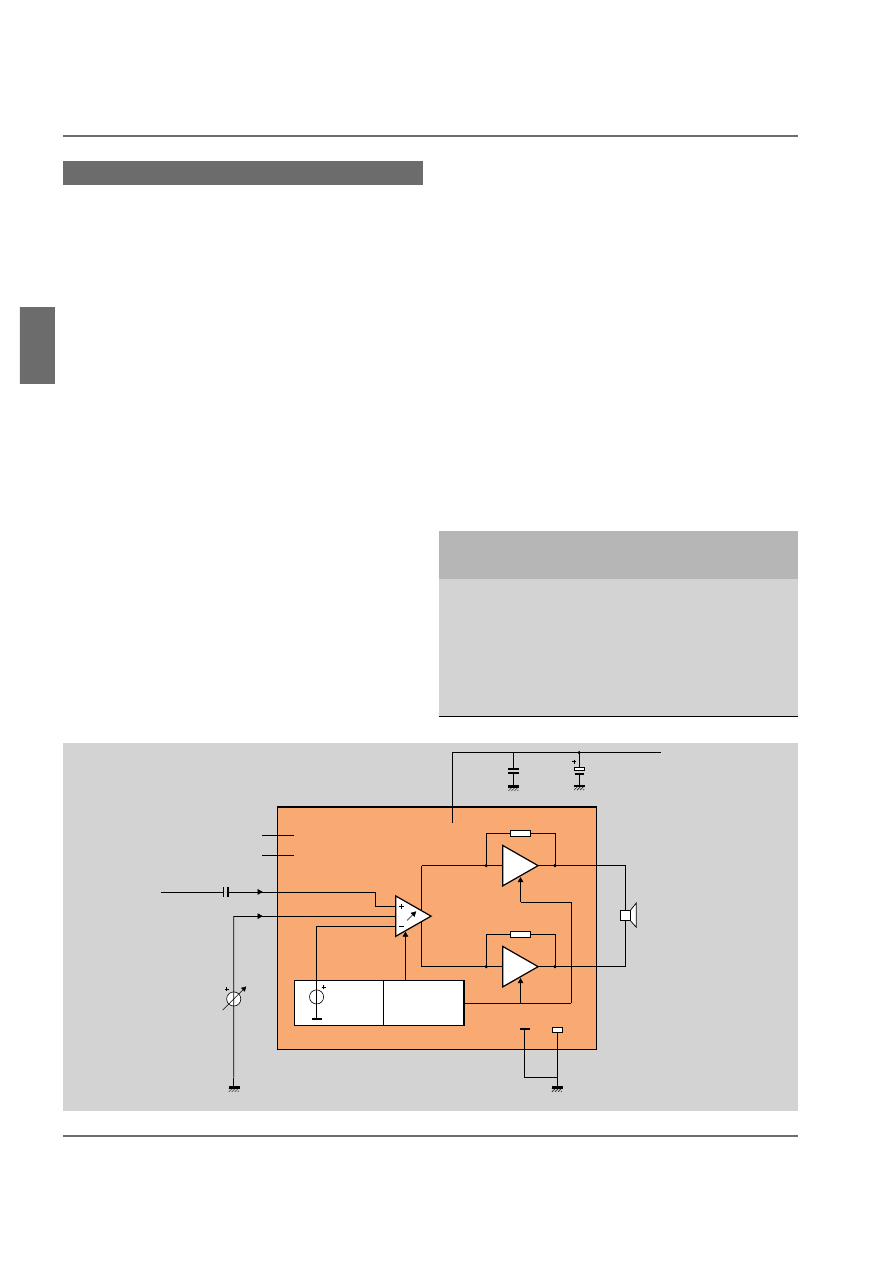
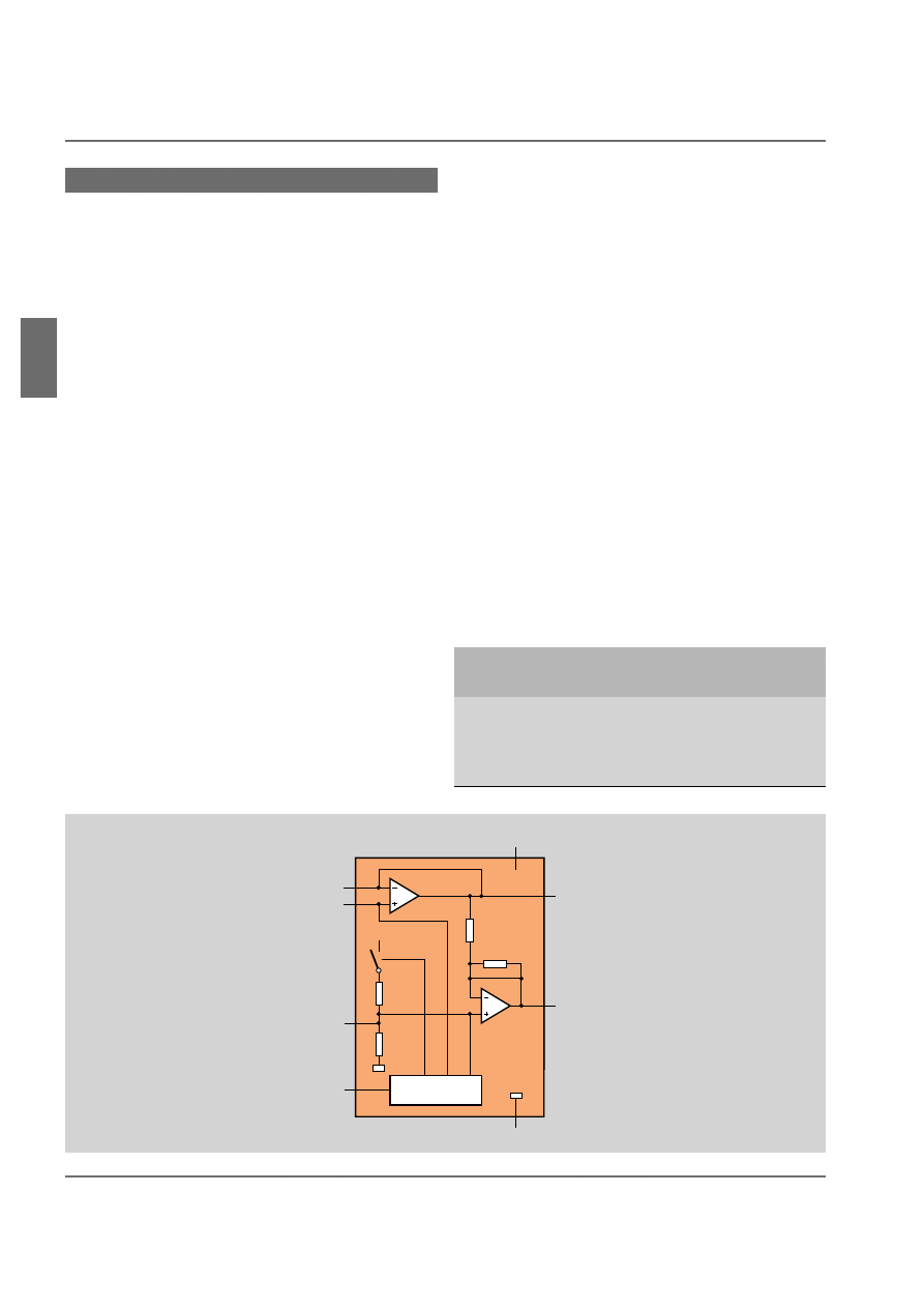
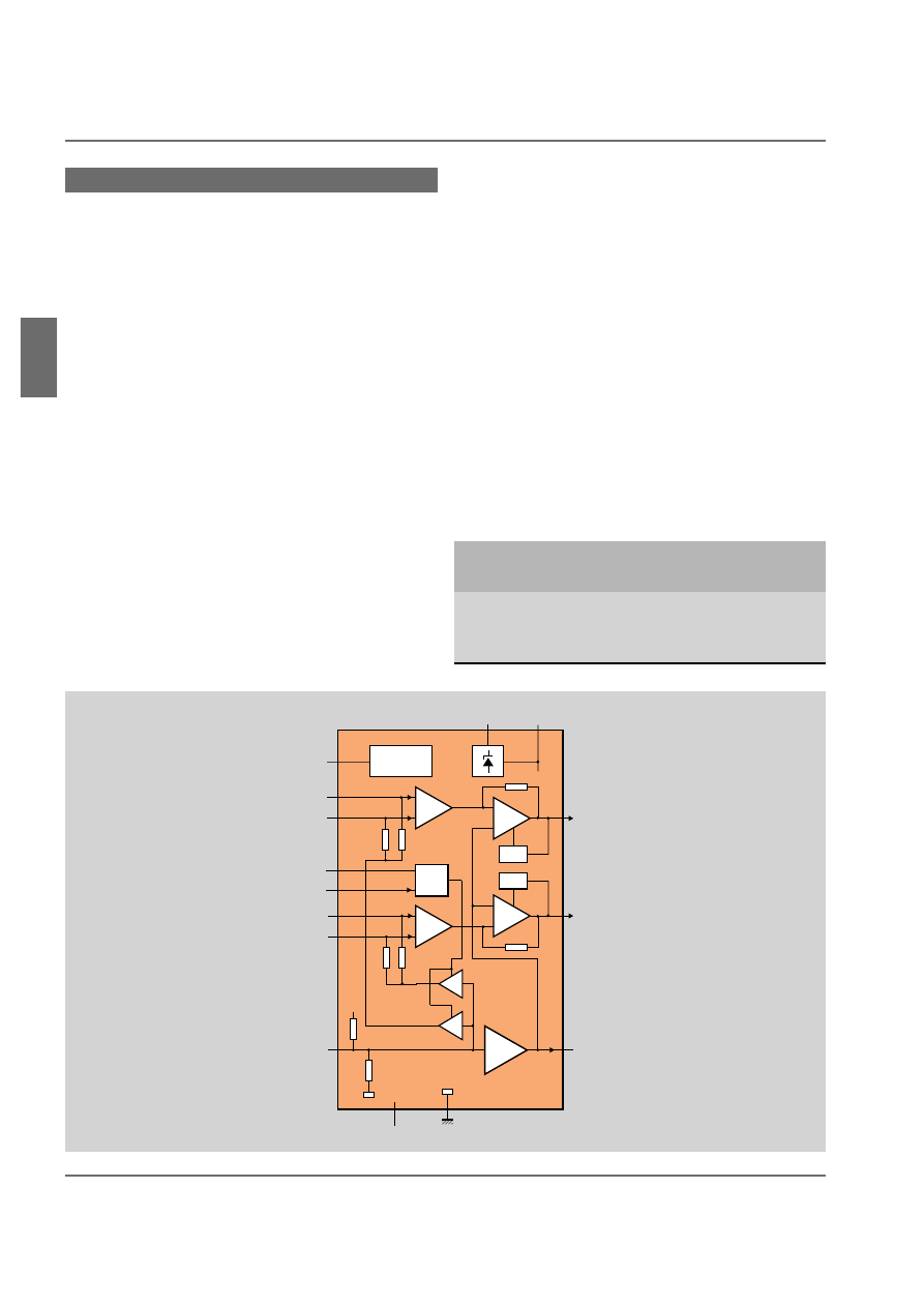
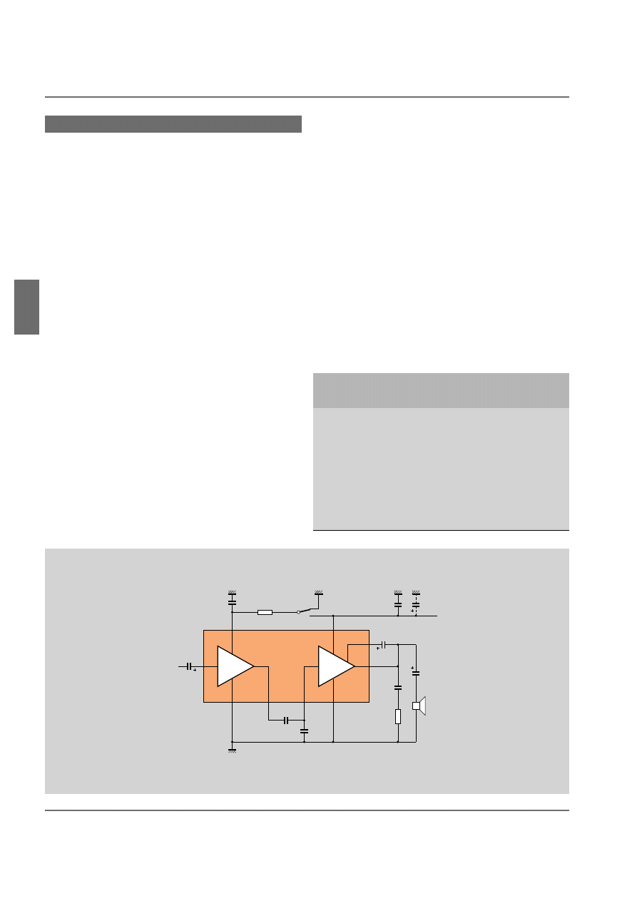
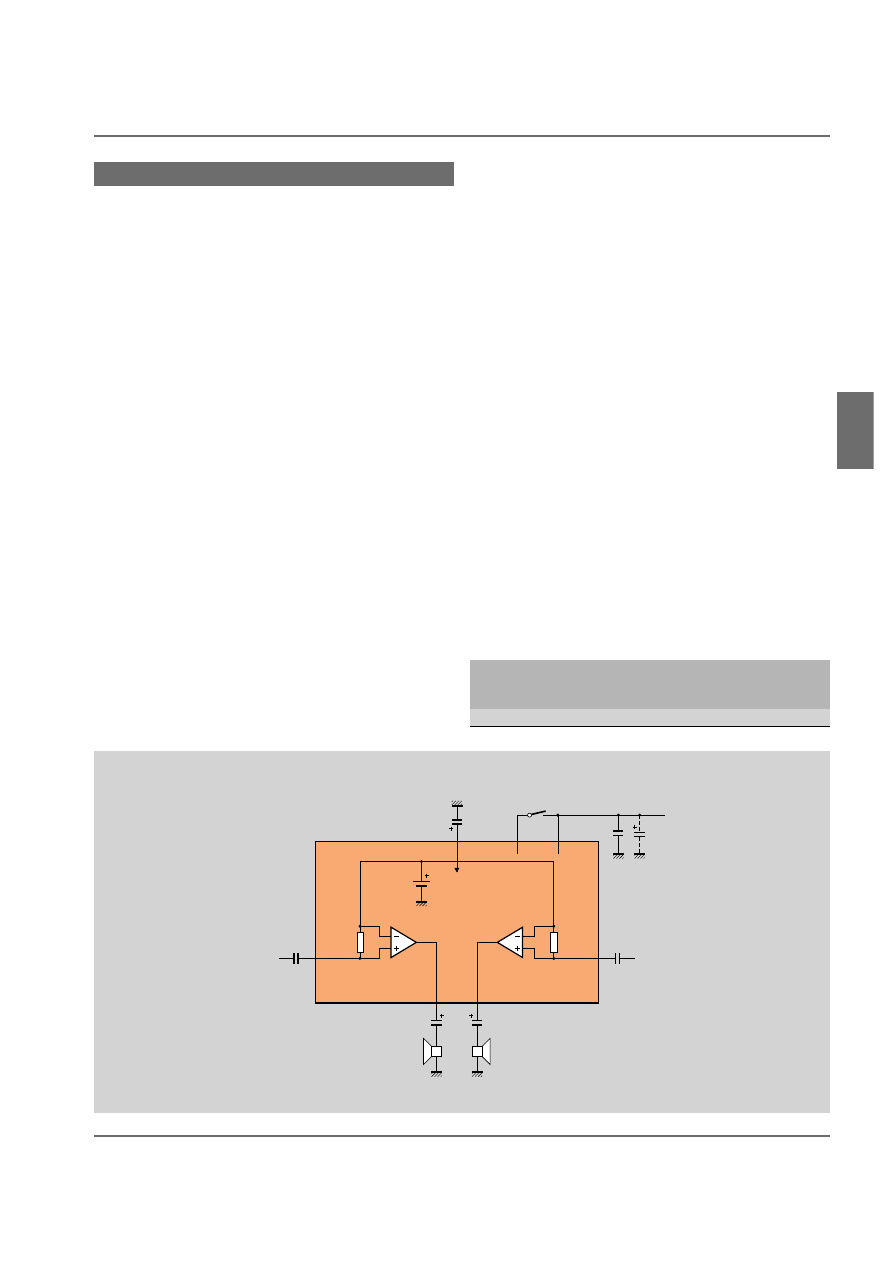
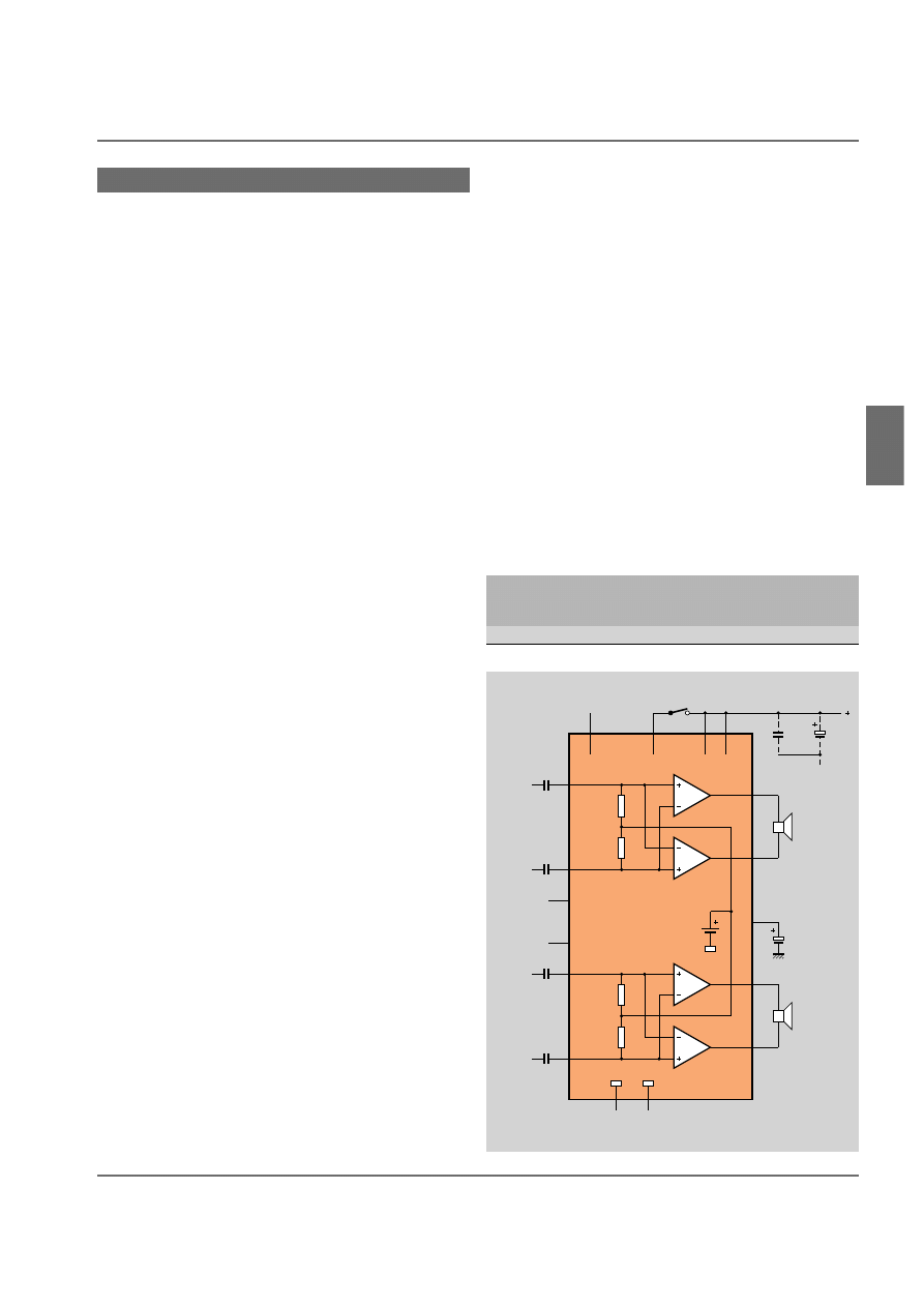
TDA1011/TDA1015
POWER OUTPUT AT d
tot
= 10%
power
supply
load
output
voltage
impedance
(W)
(V)
(
Ω
)
with bootstrapping
1
6
4
2.3
9
4
4.2
12
4
*6.5
16
4
without bootstrapping
3
12
4
* TDA1011
Preamplifier plus 6.5 W/4 W
power amplifier
■
Separate preamplifier and power amplifier
■
Thermal protection
■
High input impedance (greater than 100 k
Ω
)
■
Low current drain (typically 14 mA with a 12 V
supply)
■
Limits RF noise.
■
Minimum number of external components
■
Simple and low cost heatsinking
■
No switch-on/switch-off clicks
■
Output noise diminishes with reducing volume
These ICs are primarily for battery-powered portable recorders
and radios, the TDA1011 offering an output power of 6.5 W
and the TDA1015 and output power of 4 W. However, their
wide supply voltage ranges (TDA1011: 3.6 to 24 V, TDA1015:
3.6 to 18 V) mean they are also suitable for mains powered
equipment. The ICs come in a 9-pin medium-power plastic SIL
package and are pin compatible with each other.
MSB422
VP
input
1
µ
F
2
9
7
6
1
2
680
µ
F
3
330 k
Ω
TDA1011/
TDA1015
5
100 nF
1.8 nF
100
nF
4.7
Ω
100
µ
F
220 nF
10
µ
F
4
POWER
AMP.
PREAMP.
5.6 k
Ω
100 pF
1
µ
F
TDA1015T
500 mW amplifier
■
Separate preamplifier and power amplifier
■
Thermal protection
■
High input impedance (greater than 100 k
Ω
)
■
Low current drain (typically 14 mA with a 12 V
supply)
■
Limits RF noise
■
Few peripheral components
This amplifier is for portable and mains-powered equipment. It
delivers up to 500 mW into 32
Ω
and has a supply voltage range
from 3.6 V up to 12 V.
It comes in an 8-pin SO package for surface mounting in com-
pact circuitry such as mobile radios and telecom equipment.
POWER OUTPUT AT d
tot
= 10%
power
supply
load
output
voltage
impedance
(mW)
(V)
(
Ω
)
300
6
8
500
9
16
500
12
32
AUDIO AMPLIFIER IC
S
PORTABLE RADIO/AUDIO EQUIPMENT
MSB417
VP
input
0.1
µ
F
1
2
8
7
3
4
5
TDA1015T
6
4.7
Ω
220
µ
F
POWER
AMP.
PREAMP.
0.1
µ
F
22 nF
3-3
Audio Amplifier ICs
3
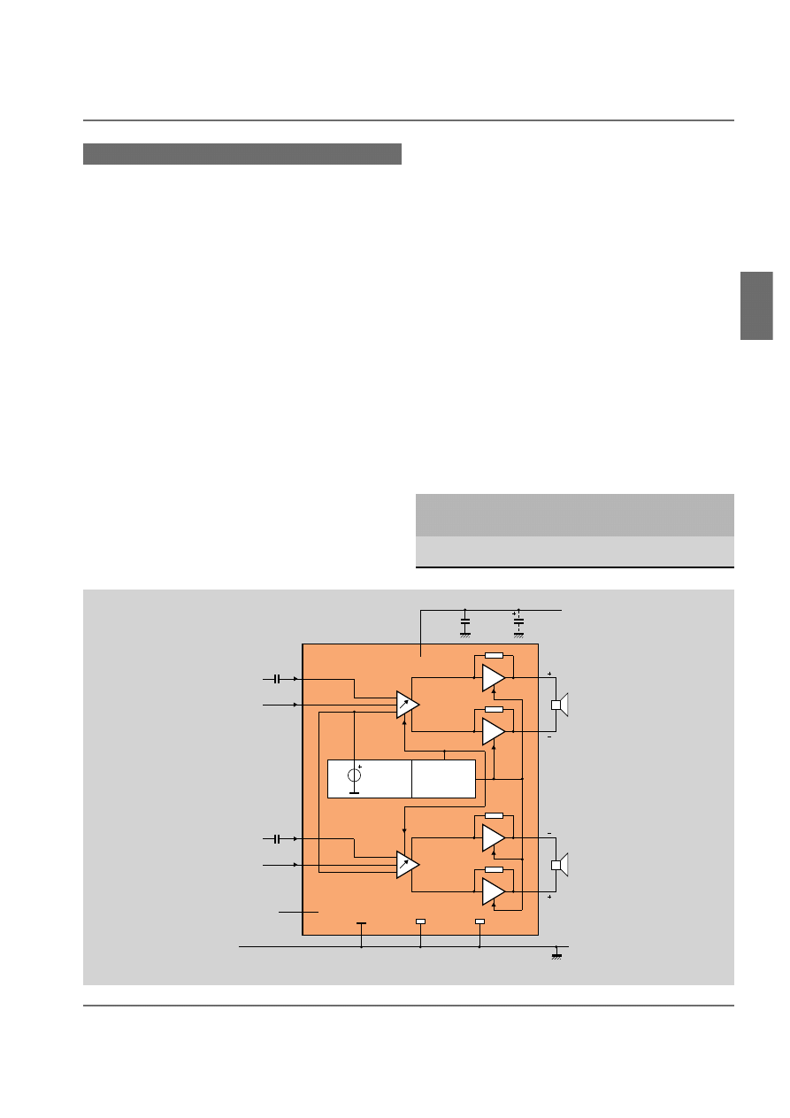
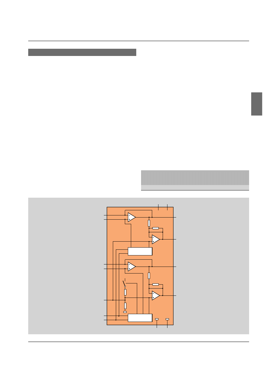
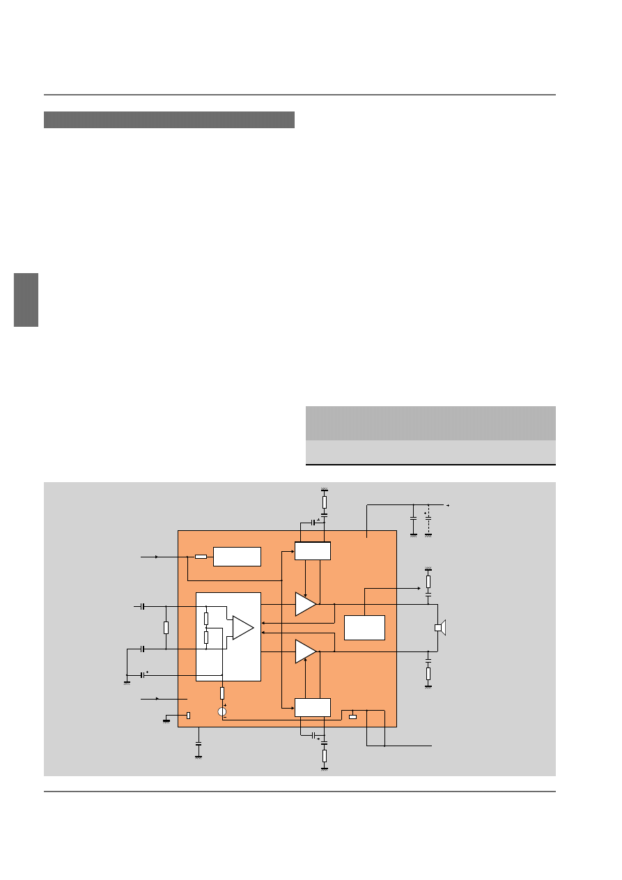
TDA1016
2 W power and record/playback preamplifier
■
Separate record/playback preamplifier and power
amplifier
■
Incorporates ALC (automatic level control) for
recording
■
Voltage stabilization (2.6 V)
■
Short-circuit protection
■
Thermal protection
■
Standby switching facility to minimize current
drain
This amplifier includes an ALC (automatic level control) circuit
and is designed specifically for recorders and radio recorders.
With an operating voltage range from 3.6 V to 15 V, it’s ideal
for a wide range of both portable and mains-powered equip-
ment. Two of these ICs can be used for stereo. The IC comes in
a 16-pin plastic DIP with internal heat spreader.
MSB421
VP
TDA1016
56
Ω
470
µ
F
POWER
AMP.
PREAMP.
1
µ
F
24 k
Ω
5.1 k
Ω
10 nF
3.3 k
Ω
470 pF
100 k
Ω
82 k
Ω
22 k
Ω
4.7 k
Ω
220 pF
10 nF
68 k
Ω
22 nF
100 k
Ω
22
µ
F
270
k
Ω
2.2
nF
1
µ
F
R
P
10 k
Ω
10 k
Ω
record-
input
playback
input
180
k
Ω
STAB
ALC
8
9
5
7
6
11
10
12
22
µ
F
22
µ
F
160
Ω
13
14
15
16
560 pF
220 pF
100
nF
2.7
Ω
4
Ω
100
µ
F
2
1
100
nF
2.2 M
Ω
22
µ
F
10 k
Ω
220 nF
stand-by switch
47
µ
F
82 k
Ω
4
3
P
R
POWER OUTPUT AT d
tot
= 10% (with bootstrapping)
power
supply
load
output
voltage
impedance
(W)
(V)
(
Ω
)
2
9
4
AUDIO AMPLIFIER IC
S
PORTABLE RADIO/AUDIO EQUIPMENT
3-4
3
Audio Amplifier ICs
TDA1308T
60 mW stereo headphone amplifier
■
Wide temperature range
■
No switch-on/off clicks
■
Excellent power supply ripple rejection
■
Low current drain (typically 3 mA with a 5 V
supply)
■
Short-circuit resistant
■
110 dB signal-to-noise ratio
■
5 V/µs slew rate at unity gain
■
Large output voltage swing
This is a class-AB stereo driver for delivering up to 60 mW into
32
Ω
headphones. It is fabricated in a 1 µm CMOS process and
is intended primarily for portable digital audio applications. It
has a supply voltage range from 3 V to 7 V.
It comes an 8-pin SO package for surface mounting.
MLB701
1
7
2
3
5
6
4
8
1 nF
3.9 k
Ω
VP
input 1
VREF
input 2
(typ. 2.5 V)
TDA1308T
1 nF
3.9 k
Ω
10 k
Ω
10 k
Ω
100
µ
F
100
µ
F
100
µ
F
100 nF
headphones
POWER OUTPUT AT d
tot
= 10%
power
supply
load
output
voltage
impedance
(mW)
(V)
(
Ω
)
60
5
32
AUDIO AMPLIFIER IC
S
PORTABLE RADIO/AUDIO EQUIPMENT
3-5
Audio Amplifier ICs
3
TDA7050(T)
150 mW BTL or 2
×
75 mW
low-voltage amplifier
■
Requires no external components in BTL
configuration
■
Operates with battery supplies from 6 V down to
1.6 V
■
Very low quiescent current (typically 3.2 mA with
3 V supply)
■
Closed-loop voltage gain fixed at 26 dB in the
stereo configuration or 32 dB in the BTL configu-
ration (floating differential input, 3 V supply and
32
Ω
load)
This low-voltage amplifier is for portable mono (BTL) or stereo
apparatus with headphones.
It comes in an 8-pin plastic DIP (TDA7050), or in an 8-pin
small outline (SO) plastic package for surface mounting
(TDA7050T).
MSB405
2
1
7
TDA7050(T)
47
µ
F
left channel
input
3
4
6
47
µ
F
right channel
input
8
100 nF
VP
22 k
Ω
22 k
Ω
5
MSA612
100
nF
P
V
7
TDA7050(T)
1
8
2
input
22 k
Ω
6
4
3
POWER OUTPUT AT d
tot
= 10%
power
supply
load
output
voltage
impedance
(mW)
(V)
(
Ω
)
mono BTL
150
4.5
64
140
3
32
stereo
2
×
75
4.5
32
2
×
35
3
32
TDA7050(T) in single-ended stereo configuration
TDA7050(T) in BTL mono configuration
AUDIO AMPLIFIER IC
S
PORTABLE RADIO/AUDIO EQUIPMENT
3-6
3
Audio Amplifier ICs
1 W/2
×
1 W BTL amplifiers
■
No external components required
■
Excellent overall stability
■
Output protected against short-circuit
■
No external heatsink required
■
Low power consumption
■
No switch-on or switch-off clicks
■
Supply voltage range of 3 V to 18 V
■
Fixed closed-loop voltage gain of 39 dB (6 V supply,
8
Ω
load)
The proprietary circuit design of these amplifiers makes use of
the bridge-tied load (BTL) principle to achieve low-voltage
operation without sacrifice of output power. They are therefore
primarily intended for battery-powered portable recorders and
radios. However, their wide supply voltage range (3 V to 18 V)
also makes them suitable for TV.
The TDA7052 comes in an 8-pin plastic DIP and is pin-
compatible with half of the TDA7053 which is in a 16-pin plas-
tic DIP.
TDA7052/TDA7053
POWER OUTPUT AT d
tot
= 10%
power
supply
load
output
voltage
impedance
(W)
(V)
(
Ω
)
TDA7052
1
6
8
2
11
25
TDA7053
2
×
1
6
8
2
×
2
11
25
14
MSA611
100
nF
220
µ
F
P
V
16
TDA7053
13
2
5
12
9
6
7
1
signal
ground 2
input 2
signal
ground 1
input 1
5 k
Ω
5 k
Ω
10
power ground 1
power ground 2
TDA7053 in BTL stereo configuration
6
MSB420
100
nF
220
µ
F
P
V
5
TDA7052
8
2
1
3
signal
ground
input
5 k
Ω
power ground
TDA7053 in BTL mono configuration
AUDIO AMPLIFIER IC
S
PORTABLE RADIO/AUDIO EQUIPMENT
3-7
Audio Amplifier ICs
3
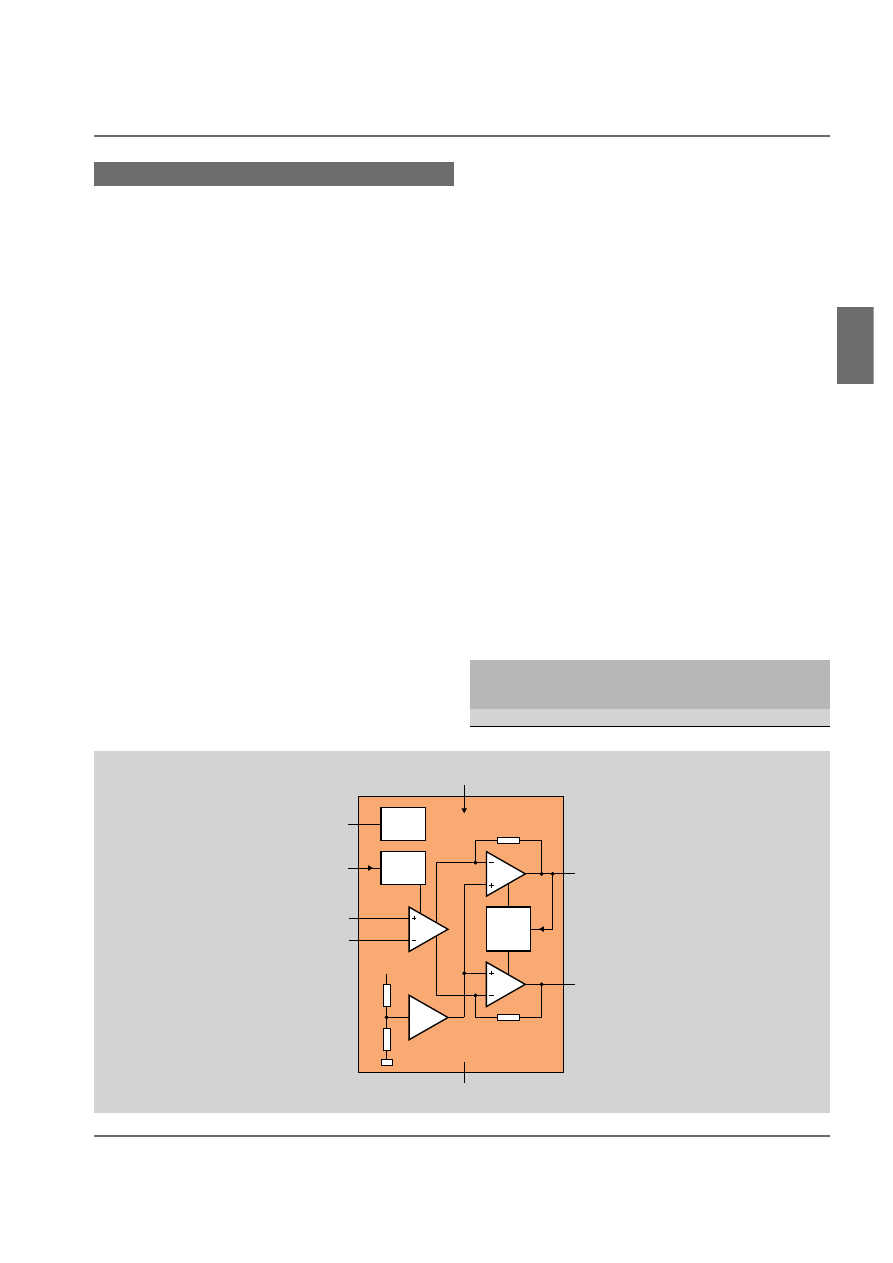
TDA7052A(AT)/TDA7052B(BT)
1 W/0.5 W BTL amplifiers with DC
volume control
■
No external components required
■
Excellent overall stability
■
Output protected against short-circuit to Vp,
ground or across load
■
No external heatsink required
■
Low power consumption
■
Thermal protection
■
Low HF radiation
■
All pins ESD protected
■
No switch-on/switch-off clicks
■
Supply voltage range of 4.5 V to 18 V
■
DC volume control
■
Mute facility
The proprietary circuit design of these amplifiers makes use of
the bridge-tied load (BTL) principle to provide low-voltage
operation without sacrifice of output power. They have fixed
voltage gain of 36 dB for the A versions, and 40 dB for the B
versions. Although they are primarily for battery-powered
POWER OUTPUT AT d
tot
= 10%
power
supply
load
output
voltage
impedance
(W)
(V)
(
Ω
)
TDA7052A/TDA7052B
1
6
8
2
12
32
TDA7052AT/TDA7052BT
0.5
6
16
input
0.47
µ
F
6
MBC281
100 nF
220
µ
F
1
2
TDA7052A/B
TDA7052AT/BT
V
P
4
5
8
V
ref
STABILIZER
TEMPERATURE
PROTECTION
3
ground
DC
volume
control
7
n.c.
AUDIO AMPLIFIER IC
S
PORTABLE RADIO/AUDIO EQUIPMENT
portable recorders, radios and telephones, their wide supply volt-
age range (4.5 V to 18 V) also makes them suitable for multi-
media and TV applications.
The amplifiers have built-in DC volume control with a logarith-
mic characteristic providing control over a typical range of
80 dB (73 dB B versions). When the DC control voltage drops
below 0.3 V (0.4 V B versions), the amplifier is muted. Except
for pin 4 (DC volume control), the amplifiers are pin-compati-
ble with the TDA7052.
They come in an 8-pin plastic DIP (TDA7052A/7052B) or in
an 8-pin small outline (SO) plastic package for surface mount-
ing (TDA7052AT/TDA7052BT).
3-8
3
Audio Amplifier ICs
TDA7053A/TDA7053AT
2
×
1 W/2
×
0.5 W BTL amplifiers with DC
volume control
■
No external components required
■
Excellent overall stability
■
Output protected against short-circuit to V
p
,
ground or across load
■
No external heatsink required
■
Low power consumption.
■
Thermal protection
■
Low HF radiation
■
All pins ESD protected
■
No switch-on/switch-off clicks
■
Supply voltage range of 4.5 V to 18 V
■
DC volume control
■
Mute facility
These amplifiers are stereo versions of the TDA7052B/
TDA7052BT. They use the same proprietary circuit design
which makes use of the bridge-tied load (BTL) principle to pro-
vide low-voltage operation without sacrifice of output power.
They have fixed voltage gain of 40 dB. Although they are pri-
POWER OUTPUT AT d
tot
= 10%
power
supply
load
output
voltage
impedance
(W)
(V)
(
Ω
)
TDA7053A
2
×
1
6
8
2
×
2
12
32
TDA7053AT
2
×
0.5
6
16
MSA718 - 2
STABILIZER
TEMPERATURE
PROTECTION
Vref
13
2
4
16
9
8
6
12
14
10
ground
7
input 2
TDA7053A
TDA7053AT
5
0.47
µ
F
input 1
DC
volume
control 1
DC
volume
control 2
0.47
µ
F
220
µ
F
100 nF
V P
AUDIO AMPLIFIER IC
S
PORTABLE RADIO/AUDIO EQUIPMENT
marily for battery-powered portable recorders, radios and tele-
phones, their wide supply voltage range (4.5 V to 18 V) also
makes them suitable for multimedia and TV applications.
The amplifiers have built-in DC volume control with a logarith-
mic characteristic providing control over a typical range of
73 dB. When the DC control voltage drops below 0.4 V, the
amplifier is muted.
They come in a 16-pin plastic DIP (TDA7053A) or in a 16-pin
small outline (SO) plastic package for surface mounting
(TDA7053AT).
3-9
Audio Amplifier ICs
3
TDA7056/TDA7057Q
3 W/2
×
3 W BTL amplifiers
■
No external components required
■
Excellent overall stability
■
Output protected against short-circuit
■
Low power consumption
■
No switch-on or switch-off clicks
■
Supply voltage range of 3 V to 18 V
■
Fixed closed-loop voltage gain of 39 dB
(11 V supply, 16
Ω
load)
These BTL amplifiers are primarily for battery-powered port-
ables. However, their wide supply voltage range (3 V to 18 V)
also makes them suitable for mains-powered applications such as
TV.
The TDA7056 comes in a 9-pin plastic SIL medium-power
package. The TDA7057Q comes in a 13-pin plastic SIL power
package with the pins bent to DIL format.
12
MSB418
100
nF
220
µ
F
P
V
13
TDA7057Q
11
2
3
10
8
4
5
1
signal
ground 2
input 2
signal
ground 1
input 1
5 k
Ω
5 k
Ω
9
power ground 1
power ground 2
POWER OUTPUT AT d
tot
= 10%
power
supply
load
output
voltage
impedance
(W)
(V)
(
Ω
)
TDA7056
3
11
16
TDA7057Q
2
×
3
11
16
TDA7057Q in BTL stereo configuration
7
MSB419
100
nF
220
µ
F
P
V
6
TDA7056
8
3
2
4
signal
ground
input
5 k
Ω
power ground
TDA7057Q in BTL configuration
AUDIO AMPLIFIER IC
S
PORTABLE RADIO/AUDIO EQUIPMENT
3-10
3
Audio Amplifier ICs
TDA7056A/TDA7056B
5 W BTL amplifiers with DC volume
control
■
No external components required
■
Excellent overall stability
■
Output protected against short-circuit to V
p
,
ground or across load
■
Low power consumption
■
No switch-on/switch-off clicks
■
DC volume control
■
Mute mode
■
Thermal protection
■
Low HF radiation
■
All pins ESD protected
These BTL amplifiers are primarily for battery-powered porta-
bles. However, their wide supply voltage range (4.5 V to 18 V)
also makes them suitable for mains-powered applications such as
multimedia and TV. They have fixed voltage gain of 36 dB for
the A version, and 40 dB for the B version.
The amplifiers have built-in DC volume control with a logarith-
mic characteristic providing control over a typical range of
80 dB (73 dB B version). When the DC control voltage drops
below 0.3 V (0.4 V B version), the amplifier is muted.
Both ICs come in a 9-pin plastic SIL package.
POWER OUTPUT AT d
tot
= 10%
power
supply
load
output
voltage
impedance
(W)
(V)
(
Ω
)
Both ICs
3.5
12
16
TDA7056A
5.0
12
8
TDA7056B
5.0
12
8
input
0.47
µ
F
7
MBC280
100 nF
220
µ
F
2
3
TDA7056A
TDA7056B
V
P
5
6
8
V
ref
STABILIZER
TEMPERATURE
PROTECTION
4
ground
DC
volume
control
1
n.c.
9
n.c.
AUDIO AMPLIFIER IC
S
PORTABLE RADIO/AUDIO EQUIPMENT
3-11
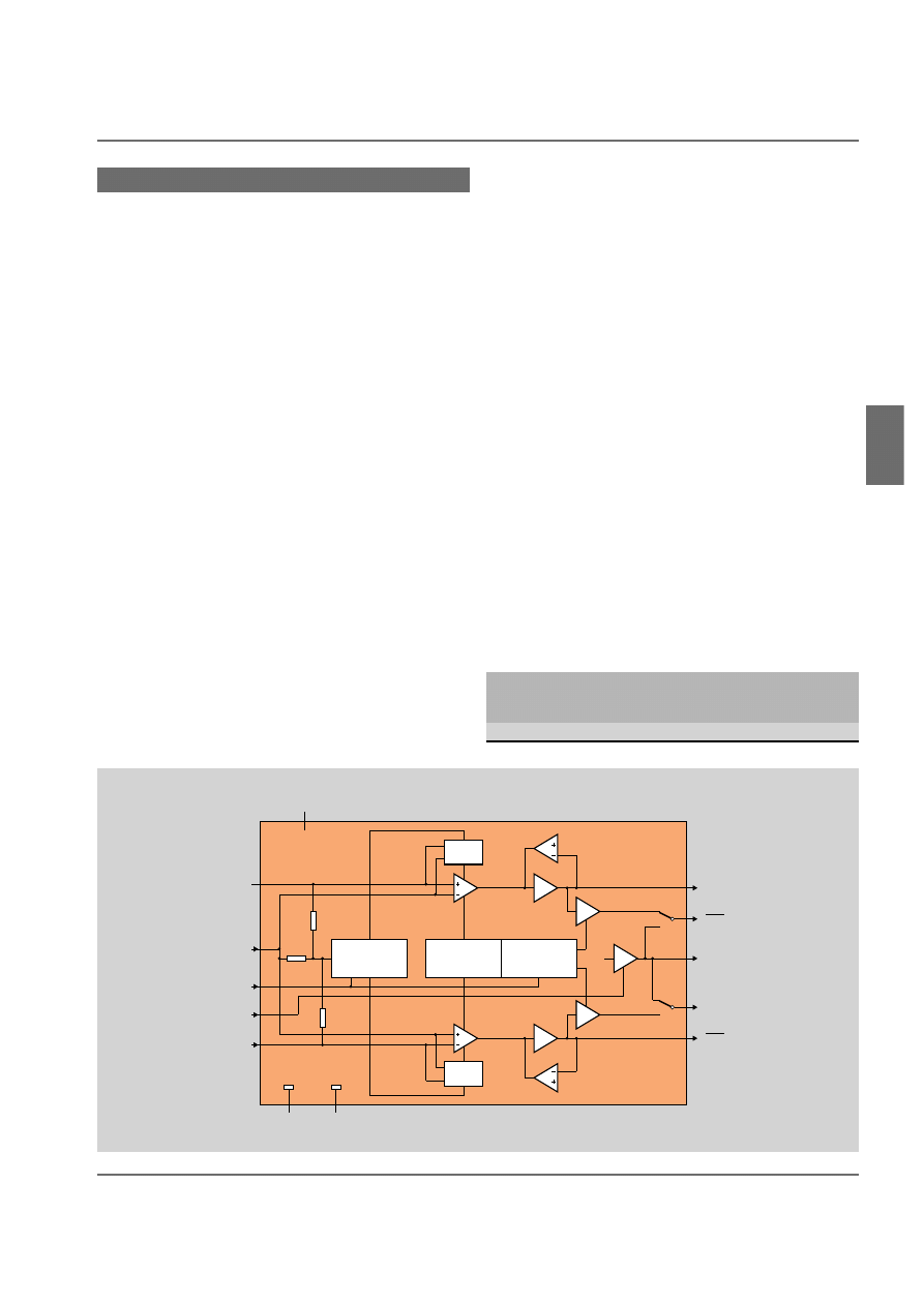
Audio Amplifier ICs
3
TDA7057AQ
2
×
5 W BTL amplifier with DC volume
control
■
No external components required
■
Excellent overall stability
■
Output protected against short-circuit to V
p
,
ground or across load
■
Low power consumption
■
No switch-on/switch-off clicks
■
DC volume control
■
Mute mode
■
Thermal protection
■
Low HF radiation
■
All pins ESD protected
This BTL amplifier is a stereo version of the TDA7056B.
Although primarily for battery-powered portables, its wide
supply voltage range (4.5 V to 18 V) also makes them suitable
for mains-powered applications such as multimedia and TV. It
has a fixed voltage gain of 40 dB.
MSA715 - 1
STABILIZER
TEMPERATURE
PROTECTION
Vref
11
1
3
13
8
7
5
10
12
9
ground
6
2
input 2
TDA7057AQ
4
0.47
µ
F
input 1
DC
volume
control 1
0.47
µ
F
DC
volume
control 2
220
µ
F
100 nF
(1)
V P
not
connected
POWER OUTPUT AT d
tot
= 10%
power
supply
load
output
voltage
impedance
(W)
(V)
(
Ω
)
2
×
3.5
12
16
2
×
5.0
12
8
AUDIO AMPLIFIER IC
S
PORTABLE RADIO/AUDIO EQUIPMENT
The amplifier has built-in DC volume control with a logarith-
mic characteristic providing control over a typical range of
73 dB. When the DC control voltage drops below 0.4 V, the
amplifier is muted.
The IC comes in a 13-pin plastic SIL package with the leads
bent to DIL format.
3-12
3
Audio Amplifier ICs
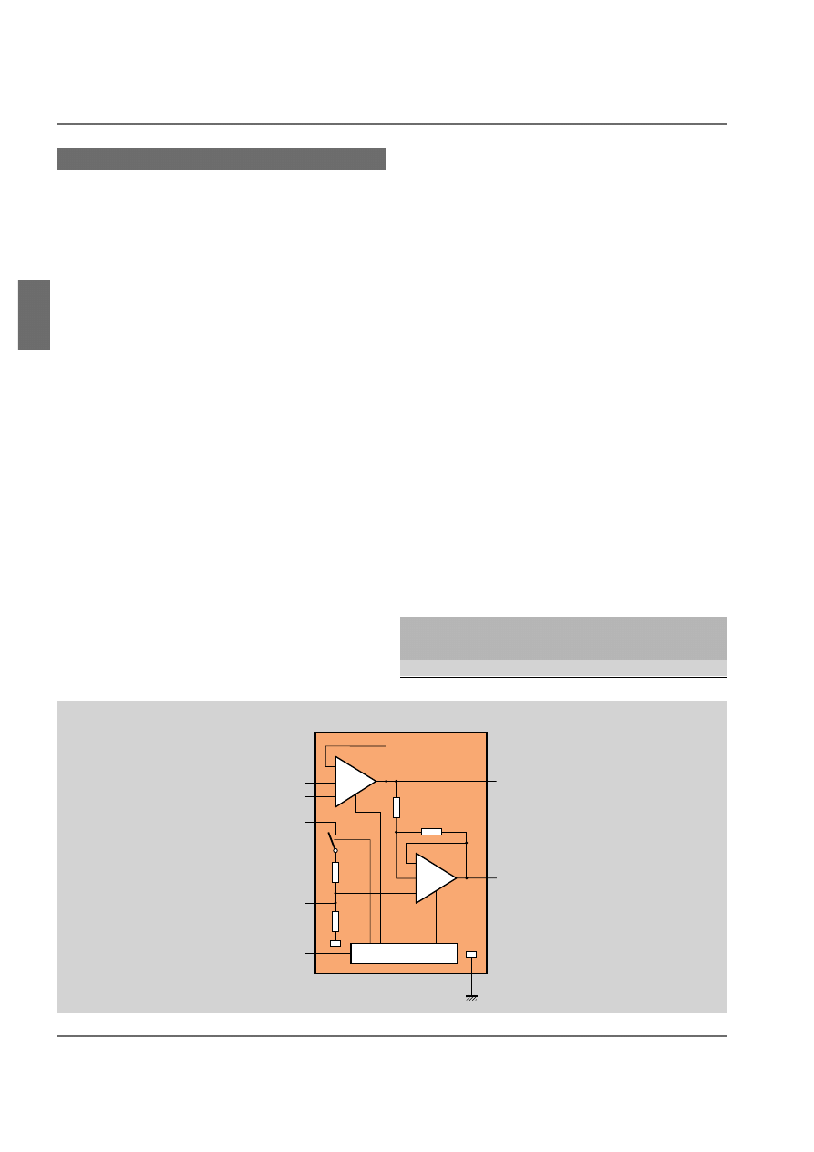
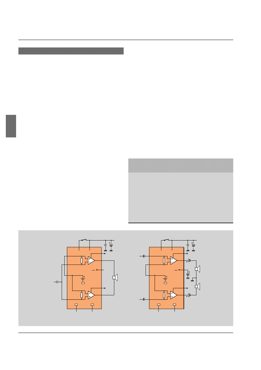
1 W BTL amplifiers
■
Few external components required
■
Low saturation voltage of output stage
■
Gain settable with external resistors
■
Standby mode controllable by CMOS-compatible
levels
■
Low standby current
■
No switch-on/switch-off clicks
■
High supply-voltage ripple rejection
■
Thermal protection
■
Outputs short-circuit safe to ground, V
CC
and
across load
■
All pins ESD protected
These amplifiers make use of the bridge-tied load (BTL) princi-
ple to achieve low-voltage operation without sacrifice of output
power. They are therefore primarily for battery-powered applica-
tions such as portable recorders and radios and cellular tele-
phones. However, their wide supply voltage range (2.2 V to
18 V) also makes them suitable for mains powered applications
such as multimedia PCs. The amplifiers also feature a
standby/mute facility to avoid switch-on/switch-off clicks.
They come in an 8-pin plastic DIP (TDA8541) or in an 8-pin
small outline (SO) plastic package for surface mounting
(TDA8541T).
MGB972
4
STANDBY/MUTE LOGIC
3
6
2
1
7
8
5
R
R
20 k
Ω
20 k
Ω
IN
−
IN
+
VCC
SVR
MODE
OUT
−
OUT
+
GND
−
−
+
−
−
+
TDA8541
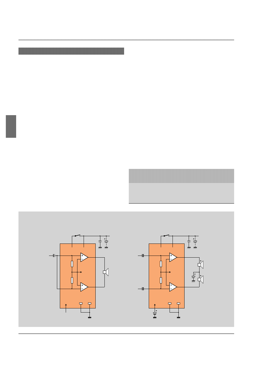
TDA8541/TDA8541T
POWER OUTPUT AT d
tot
= 10%
power
supply
load
output
voltage
impedance
(W)
(V)
(
Ω
)
1
5
8
AUDIO AMPLIFIER IC
S
PORTABLE RADIO/AUDIO EQUIPMENT
3-13
Audio Amplifier ICs
3
2
×
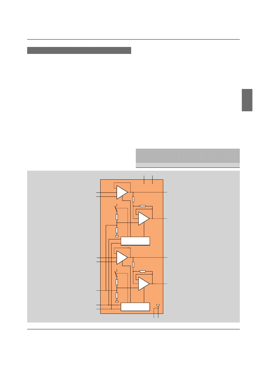
1 W BTL amplifiers
■
Few external components required
■
Low saturation voltage of output stage
■
Gain settable with external resistors
■
Standby mode controllable by CMOS-compatible
levels
■
Low standby current
■
No switch-on/switch-off clicks
■
High supply-voltage ripple rejection
■
Thermal protection
■
Outputs short-circuit safe to ground, V
CC
and
across load
■
All pins ESD protected
MGB975
STANDBY/MUTE LOGIC
R
R
20 k
Ω
20 k
Ω
INL
−
INL
+
VCCL
OUTL
−
OUTL
+
−
−
+
−
−
+
STANDBY/MUTE LOGIC
R
R
20 k
Ω
20 k
Ω
INR
−
INR
+
VCCR
SVR
MODE
OUTR
−
OUTR
+
−
−
+
−
−
+
BTL/SE
LGND
RGND
VCCL VCCR
16
9
15
2
10
7
1
8
14
13
11
12
4
3
5
TDA8542
TDA8542/TDA8542T
POWER OUTPUT AT d
tot
= 10%
power
supply
load
output
voltage
impedance
(W)
(V)
(
Ω
)
2
×
1
5
8
AUDIO AMPLIFIER IC
S
PORTABLE RADIO/AUDIO EQUIPMENT
These amplifiers are stereo versions of the TDA8541/
TDA8541T. They are primarily for battery-powered applica-
tions such as portable recorders and radios and cellular tele-
phones. However, their wide supply voltage range (2.2 V to
18 V) also makes them suitable for mains powered applications
such as multimedia PCs. The amplifiers also feature a standby/
mute facility to avoid switch-on/switch-off clicks.
Besides audio applications, they are also suitable for use as elec-
tric motor drivers in, for example, CD servo systems.
The amplifiers come in a 16-pin plastic DIP (TDA8542) or in a
16-pin small outline (SO) plastic package for surface mounting
(TDA8542T).
3-14
3
Audio Amplifier ICs
2 W BTL amplifiers
■
Few external components required
■
Low saturation voltage of output stage
■
Gain settable with external resistors
■
Standby mode controllable by CMOS-compatible
levels
■
Low standby current
■
No switch-on/switch-off clicks
■
High supply-voltage ripple rejection
■
Thermal protection
■
Outputs short-circuit safe to ground, V
CC
and
across load
■
All pins ESD protected
These BTL amplifiers are primarily for battery-powered applica-
tions such as portable recorders and radios and cellular tele-
phones. However, their wide supply voltage range (2.2 V to
18 V) also makes them suitable for mains powered applications
such as multimedia PCs. The amplifiers also feature a standby/
mute facility to avoid switch-on/switch-off clicks.
They come in a 16-pin plastic DIP (TDA8543) or in an 16-pin
small outline (SO) plastic package for surface mounting
(TDA8543T).
MSC249
VCC
VCC
20 k
Ω
STANDBY/MUTE
LOGIC
20 k
Ω
GND
R
R
6
12
5
4
3
13
OUT
+
OUT
−
IN
+
SVR
MODE
IN
−
14
11
TDA8543
TDA8543/TDA8543T
POWER OUTPUT AT d
tot
= 10%
power
supply
load
output
voltage
impedance
(W)
(V)
(
Ω
)
1
5
8
2
7.5
8
1.4
7.5
16
2
9
16
1.3
9
25
AUDIO AMPLIFIER IC
S
PORTABLE RADIO/AUDIO EQUIPMENT
3-15
Audio Amplifier ICs
3
2
×
1 W BTL amplifiers with independent
channel standby selection
■
Independent standby selection of output channels
■
Few external components required
■
Low saturation voltage of output stage
■
Gain settable with external resistors
■
Standby mode controllable by CMOS-compatible
levels
■
Low standby current
■
No switch-on/switch-off clicks
■
High supply-voltage ripple rejection
■
Thermal protection
■
Outputs short-circuit safe to ground, V
CC
and
across load
■
All pins ESD protected
MSC261
VCC
VCC1
20 k
Ω
STANDBY/MUTE
LOGIC
20 k
Ω
GND1
R
R
11
16
12
4
3
1
GND2
8
OUT2
+
OUT2
−
IN2
+
SVR
MODE
5
SELECT
IN2
−
7
10
STANDBY/MUTE
LOGIC
R
R
14
13
OUT1
+
OUT1
−
IN1
+
IN1
−
2
15
VCC2
9
TDA8547
TDA8547/TDA8547T
POWER OUTPUT AT d
tot
= 10%
power
supply
load
output
voltage
impedance
(W)
(V)
(
Ω
)
2
×
1
5
8
AUDIO AMPLIFIER IC
S
PORTABLE RADIO/AUDIO EQUIPMENT
These BTL stereo amplifiers incorporate standby/mute logic that
allows either one of the output channels to be switched into a
standby condition. This feature can be used, for example, for
loudspeaker selection. The amplifiers are primarily for battery-
powered applications such as portable recorders and radios and
cellular telephones. However, their wide supply voltage range
(2.2 V to 18 V) also makes them suitable for mains powered
applications such as multimedia PCs.
The amplifiers come in a 16-pin plastic DIP (TDA8547) or in a
16-pin small outline (SO) plastic package for surface mounting
(TDA8547T).
3-16
3
Audio Amplifier ICs
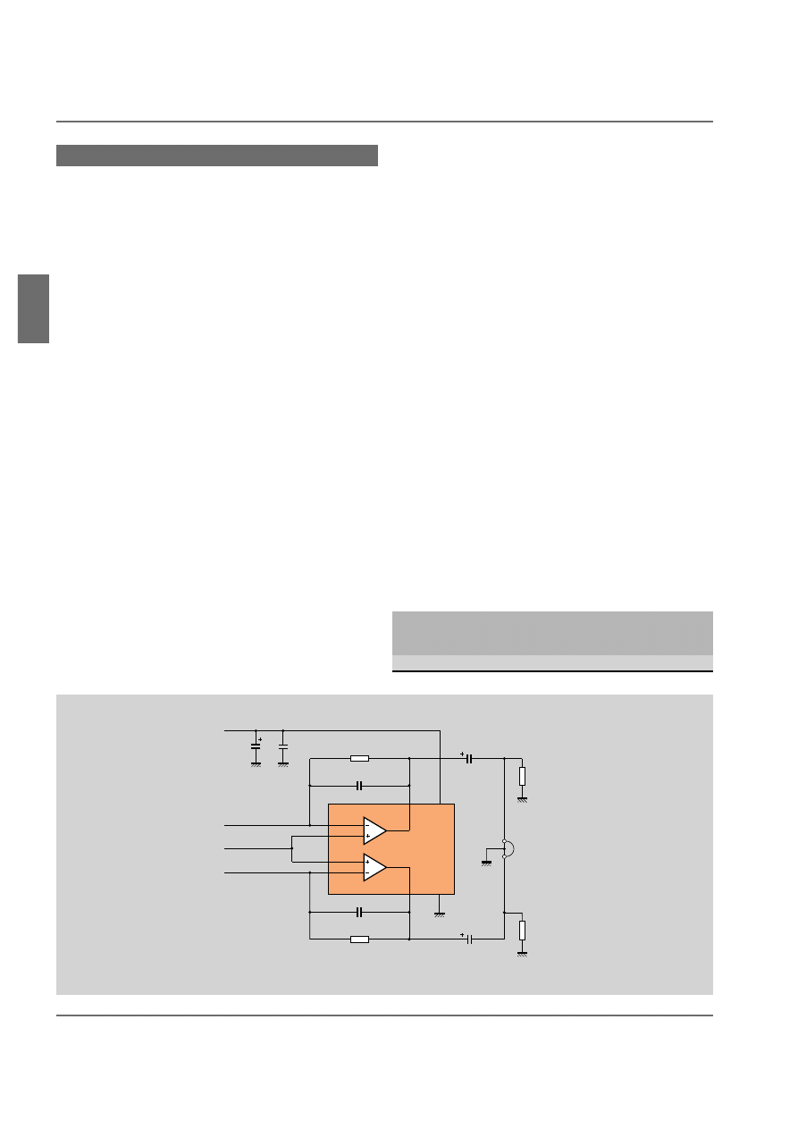
1 W BTL amplifiers with digital volume
control
■
One-pin digital volume control (volume setting
with up/down pulses)
■
Few external components required
■
Low saturation voltage of output stage
■
Standby mode controllable by CMOS-compatible
levels
■
Low standby current
■
No switch-on/switch-off clicks
■
High supply-voltage ripple rejection
■
Thermal protection
■
Outputs short-circuit safe to ground, V
CC
and
across load
■
All pins ESD protected
These BTL mono amplifiers feature digital volume control and
standby/mute logic. They are primarily for battery-powered
applications such as portable recorders/radios and cellular tele-
phones but they are also ideally suited for use in, for example,
personal computers.
The amplifiers come in an 8-pin plastic DIP (TDA8551) or in
an 8-pin small outline (SO) plastic package for surface mount-
ing (TDA8551T).
MSC262
STANDBY/MUTE
OPER
GND
R
VCC
R
20 k
Ω
7
MODE
2
OUT
+
5
OUT
+
8
6
VOLUME
CONTROL
TDA8551
SLAVE
MASTER
up/down
in
VCC
1
4
SVT
3
50 k
Ω
50 k
Ω
5 k
Ω
TDA8551/TDA8551T
POWER OUTPUT AT d
tot
= 10%
power
supply
load
output
voltage
impedance
(W)
(V)
(
Ω
)
1
5
8
AUDIO AMPLIFIER IC
S
PORTABLE RADIO/AUDIO EQUIPMENT
3-17
Audio Amplifier ICs
3
Low-voltage BTL mono amplifiers
■
Operating voltages down to 1.8 V
■
Very low quiescent current
■
Low distortion
■
No external components required
■
Differential inputs
■
Standby mode
■
No switch-on/switch-off clicks
■
Outputs short-circuit safe to ground, V
CC
and
across load
■
All pins ESD protected
These BTL mono amplifiers operate at voltages from as low as
1.8 V up to a maximum of 18 V. They also consume very little
quiescent current. The amplifiers are therefore ideally suited to
battery-powered applications (2
×
1.5 V cells) in, for example,
cellular telephones and personal audio equipment. Moreover, a
dynamic quiescent controller (DQC) feature automatically
increases quiescent current at higher frequencies to minimize
HF cross-over distortion. The amplifiers also feature a standby/
mute facility to avoid switch-on/switch-off clicks.
They come in an 8-pin plastic DIP (TDA8558) or in an 8-pin
small outline (SO) plastic package for surface mounting
(TDA8558T).
MSC263
VP
OUT
−
OUT
+
5
7
8
1
TDA8558
OA
GND
DQC
OA
OA
STANDBY
4
2
3
8
MUTE
INPUT
INPUT
LOGIC
REF
VP
VP
POWER OUTPUT AT d
tot
= 10%
power
supply
load
output
voltage
impedance
(W)
(V)
(
Ω
)
0.125
3
25
TDA8558/TDA8558T
AUDIO AMPLIFIER IC
S
PORTABLE RADIO/AUDIO EQUIPMENT
3-18
3
Audio Amplifier ICs
Low-voltage BTL stereo amplifiers
■
Operating voltages down to 1.9 V
■
Very low quiescent current
■
Low distortion
■
Few external components required
■
Differential inputs
■
Can be used as a mono amplifier in BTL or stereo
single-ended (SE) mode
■
SE mode without need of capacitor in series with
the loudspeaker
■
Mute and standby mode
■
No switch-on/switch-off clicks
■
Outputs short-circuit safe to ground, V
CC
and
across load
■
All pins ESD protected
These BTL stereo amplifiers operate at voltages from as low as
1.9 V up to a maximum of 30 V and they consume very little
quiescent current. The amplifiers are therefore ideally suited to
+
−
+
−
+
−
+
−
OA
INPUT
LOGIC
V/I
REFERENCE
V/I
1
STANDBY
−
INV1
INV1
−
INV2
INV2
MUTE
MODE
SVRR
n.c.
GND
2
3
5
6
4
12
BUFFER
OUT2
OUT1
MGD115
11
14
16
15
13
9,10
7
8
VP
VP
VP1
VP2
BUFFER
OA
50 k
Ω
50 k
Ω
50
k
Ω
50
k
Ω
TDA8559
DQC
DQC
TDA8559/TDA8559T
POWER OUTPUT AT d
tot
= 10%
power
supply
load
output
voltage
impedance
(W)
(V)
(
Ω
)
0.035
3
32
BTL mode
0.140
3
25
AUDIO AMPLIFIER IC
S
PORTABLE RADIO/AUDIO EQUIPMENT
battery-powered applications (2
×
1.5 V cells) in, for example,
personal audio equipment. They can also be used as a mono
amplifier (e.g. in cellular phones) and as a line driver in mains-
powered applications without need of any external components.
A dynamic quiescent controller (DQC) feature automatically
increases quiescent current at higher frequencies to minimize
HF cross-over distortion. The amplifiers also feature a standby/
mute facility to avoid switch-on/switch-off clicks.
They come in a 16-pin plastic DIP (TDA8559) or in a 16-pin
small outline (SO) plastic package for surface mounting
(TDA8559T).

4-1
Audio Amplifier ICs
4
CAR RADIOS/
POWER BOOSTERS
CAR RADIOS/
POWER BOOSTERS
4-2
Audio Amplifier ICs
4
MSB412
VP
input
1
µ
F
8
9
7
6
1
2
1000
µ
F
3
330 k
Ω
TDA1010A
5
stand-by
switch
100 nF
1 nF
100
nF
4.7
Ω
R L
100
µ
F
100 nF
680
µ
F
100 nF
4
POWER
AMP.
PREAMP.
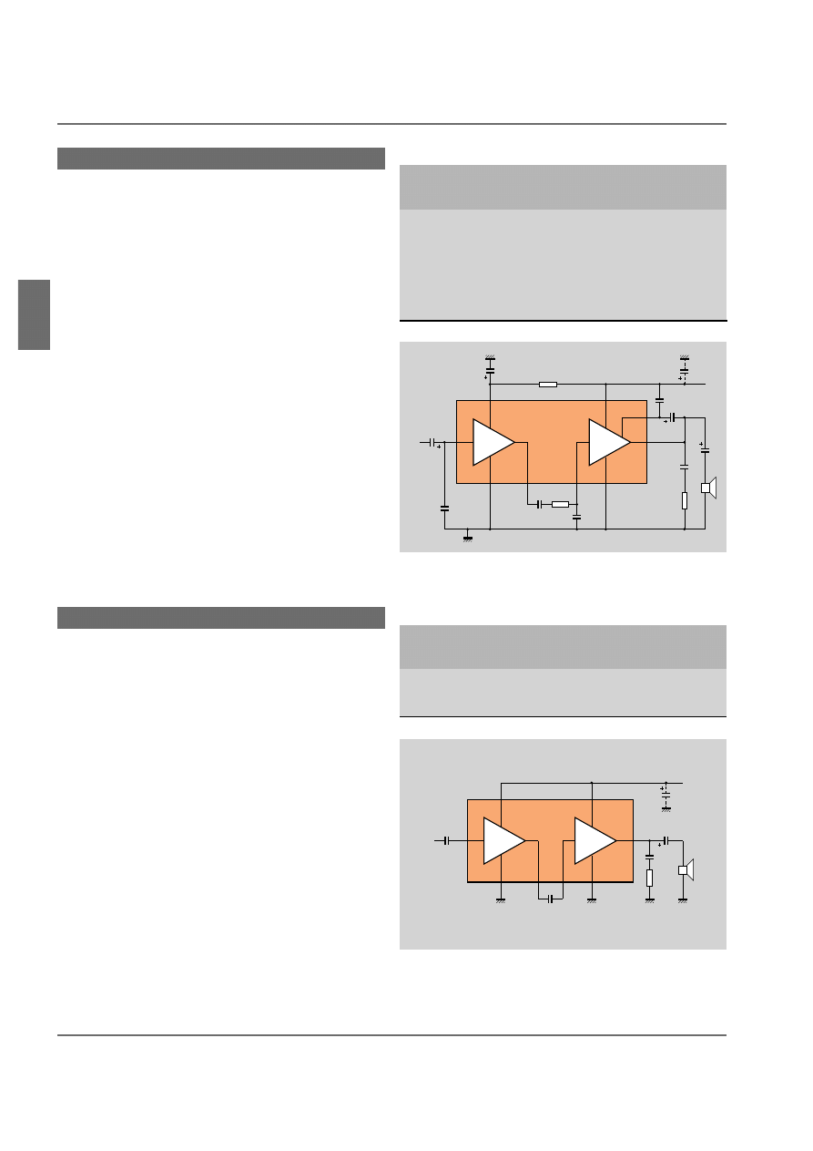
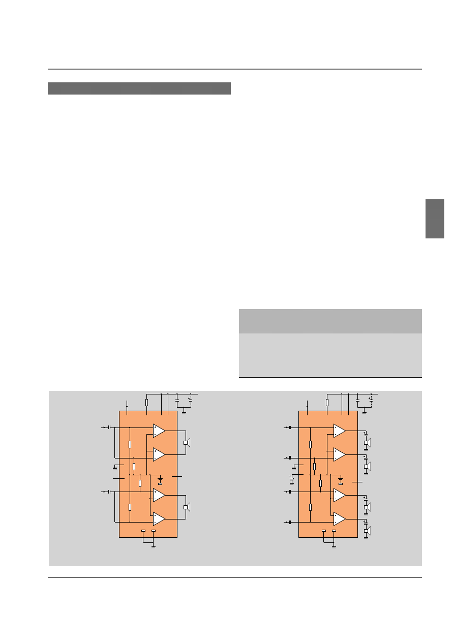
TDA1010A/TDA1020
Preamplifier plus 3.4 to 12 W power
amplifier
■
Separate preamplifier and power amplifier allows
standby switching
■
Low-cost of external components
■
Good ripple rejection
■
Thermal protection
■
Output protected against AC short-circuit to
ground
■
Load dump protection allows the circuit to
tolerate supply voltages as high as 45 V without
damage
■
High frequency limiting beyond the audible range
in the pre-amplifier and power amplifier suppress-
es supply interference and ignition noise
■
Standby switching feature with low current
consumption (<1 mA)
Although these mono amplifiers are primarily for use in car
radios, their wide supply voltage range (6 V to 24 V) also makes
them attractive for mains-powered radios and tape recorders
requiring output powers up to 12 W.
They come in a 9-pin plastic SIL medium-power packages for
easy mounting.
POWER OUTPUT AT d
tot
= 10%
power
supply
load
output
voltage
impedance
(W)
(V)
(
Ω
)
without bootstrap
5.5
14.4
4
with bootstrap capacitor (TDA1010A/1020)
3.4
14.4
8
6.2
14.4
4
6.4/12
14.4
2
with additional 220
Ω
bootstrap resistor between pins 3 and 4
(TDA1010A only)
9
14.4
2
10
18
2
AUDIO AMPLIFIER IC
S
CAR RADIOS/POWER BOOSTERS
4-3
Audio Amplifier ICs
4
MSB411
VP
100 k
Ω
1 k
Ω
input
0.1
µ
F
2
1
6
4.7
µ
F
100
µ
F
5
0.1
µ
F
12
13
0.1
µ
F
22
Ω
11
10
100 k
Ω
100 k
Ω
TDA1510AQ
TDA1515BQ
3
100
µ
F
stand-by switch
4.7
Ω
100
µ
F
1
mF
1
mF
0.1
µ
F
100 k
Ω
4.7
Ω
1 k
Ω
4.7
µ
F
0.1
µ
F
9
8
7
TDA1510AQ/TDA1515BQ
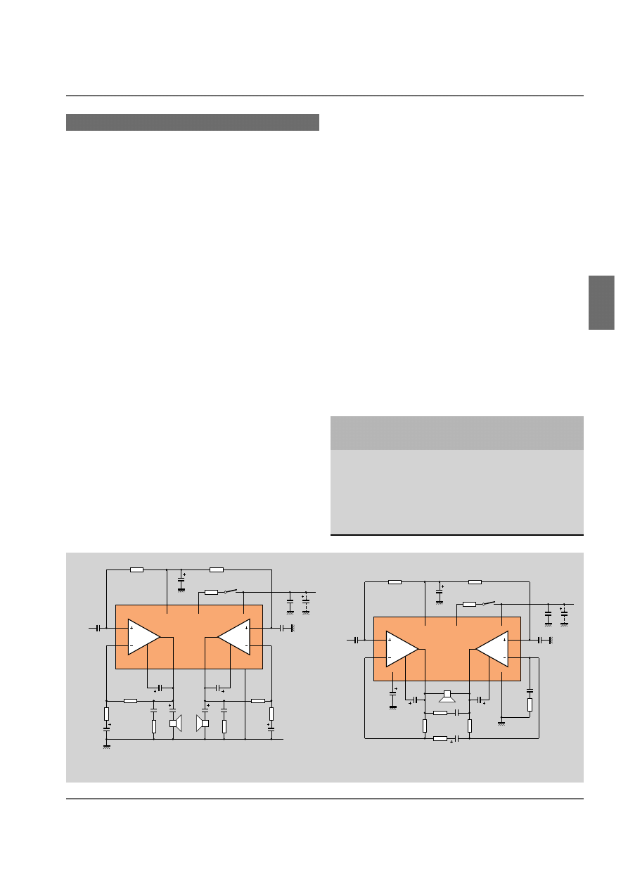
24 W BTL or 2
×
12 W amplifiers
■
Low offset voltage at output (<50 mV) – important
for BTL
■
Externally adjustable voltage gain range of 32 dB
to 56 dB in BTL configuration and 26 dB to 50 dB
in stereo configuration (14.4 V supply, 4
Ω
load)
■
High ripple rejection (50 dB at 1 kHz, R
s
= 0
Ω
)
■
Load dump and SOAR protection
■
Protection against AC short-circuit from output to
ground
■
Thermal protection
■
Internally limited bandwidth for rejection of HF
interference
■
Low standby current (<2 mA) to simplify switching
■
Few external components needed
Additional features of the TDA1515BQ
■
Low standby current (<100 µA) which allows
switching via TTL circuitry
■
Outputs protected against AC and DC short-
circuit to ground
■
Loudspeaker protection in BTL configuration
■
Outputs protected against short-circuit to ground
in BTL configuration
■
Protected against reverse polarity supply voltage
POWER OUTPUT AT d
tot
= 10%
power
supply
load
output
voltage
impedance
(W)
(V)
(
Ω
)
mono BTL with bootstrap capacitors
24
14.4
4
stereo with bootstrap capacitors
2
×
7
14.4
4
2
×
12
14.4
2
stereo without bootstrap capacitors
2
×
6
14.4
4
These class-B output amplifiers can be used in car audio systems
to drive loads down to 1.6
Ω
. They have externally adjustable
voltage gain.
They come in 13-pin plastic SIL power packages with the pins
bent to DIL format.
MSB410
VP
4.7
Ω
100 k
Ω
input
330 pF
680
Ω
0.22
µ
F
2
1
4
6
47
µ
F
100
µ
F
(1)
5
0.1
µ
F
100 k
Ω
2 k
Ω
4.7
µ
F
100
µ
F
(1)
TDA1515B only
9
8
7
12
13
0.22
µ
F
22
Ω
11
10
100 k
Ω
100 k
Ω
TDA1510AQ
TDA1515BQ
3
47
µ
F
stand-by switch
0.1
µ
F
TA1510AQ/TDA1515BQ in single-ended stereo configuration
TA1510AQ/TDA1515BQ in BTL mono configuration
AUDIO AMPLIFIER IC
S
CAR RADIOS/POWER BOOSTERS
4-4
Audio Amplifier ICs
4
MSB259
100 nF
2.2
mF
P
V
3
power
ground
5
60 k
Ω
TDA1516BQ
TDA1518BQ
11
10
1
stand-by switch
220 nF
input 1
13
220 nF
input 2
7
6
to VP
1 mF
2
100
µ
F
input ref.
voltage
4
9
8
to VP
1 mF
12
VP
2
signal
ground
100 nF
2.2
mF
P
V
3
power
ground
5
TDA1516BQ/CQ
TDA1518BQ
11
10
1
stand-by switch
13
220 nF
input
7
6
to VP
2
input ref.
voltage
4
9
60 k
Ω
8
to VP
12
VP
2
signal
ground
60 k
Ω
60 k
Ω
TDA1516BQ/TDA1516CQ/TDA1518BQ
24 W BTL or 2
×
12 W amplifiers
■
No external components in BTL configuration
■
Low offset voltage (100 mV) at output (250 mV for
TDA1518BQ) – important for BTL
■
Fixed closed-loop voltage gain (14.4 V supply, 4
Ω
load) of 26 dB for BTL (TDA1516BQ and
TDA1516CQ) and 20 dB for stereo (TDA1516BQ).
The figures for the TDA1518BQ are 46 dB (BTL)
and 40 dB (stereo)
■
High supply voltage ripple rejection (48 dB
between 100 Hz and 10 kHz, R
s
= 0
Ω
)
■
Load dump protection
■
Output protected against AC and DC short-circuit
to ground or supply rail
■
Thermal protection
■
Reverse polarity safe
■
Standby feature with switch-on voltage of 0 V to
2 V at pin 11 and a switch-on current of only 12 µA
to allow use of an inexpensive switch. The standby
supply current is <100 µA. The voltage at pin 11
for normal operation is >8.5 V
■
Mute facility with switch-on voltage of 3 V to 6.4 V
at pin 11 to eliminate switch-on/switch-off clicks.
The supply current in the muted condition is
40 mA
■
Identical inputs (inverting and non-inverting)
■
Few external components needed in stereo
configuration
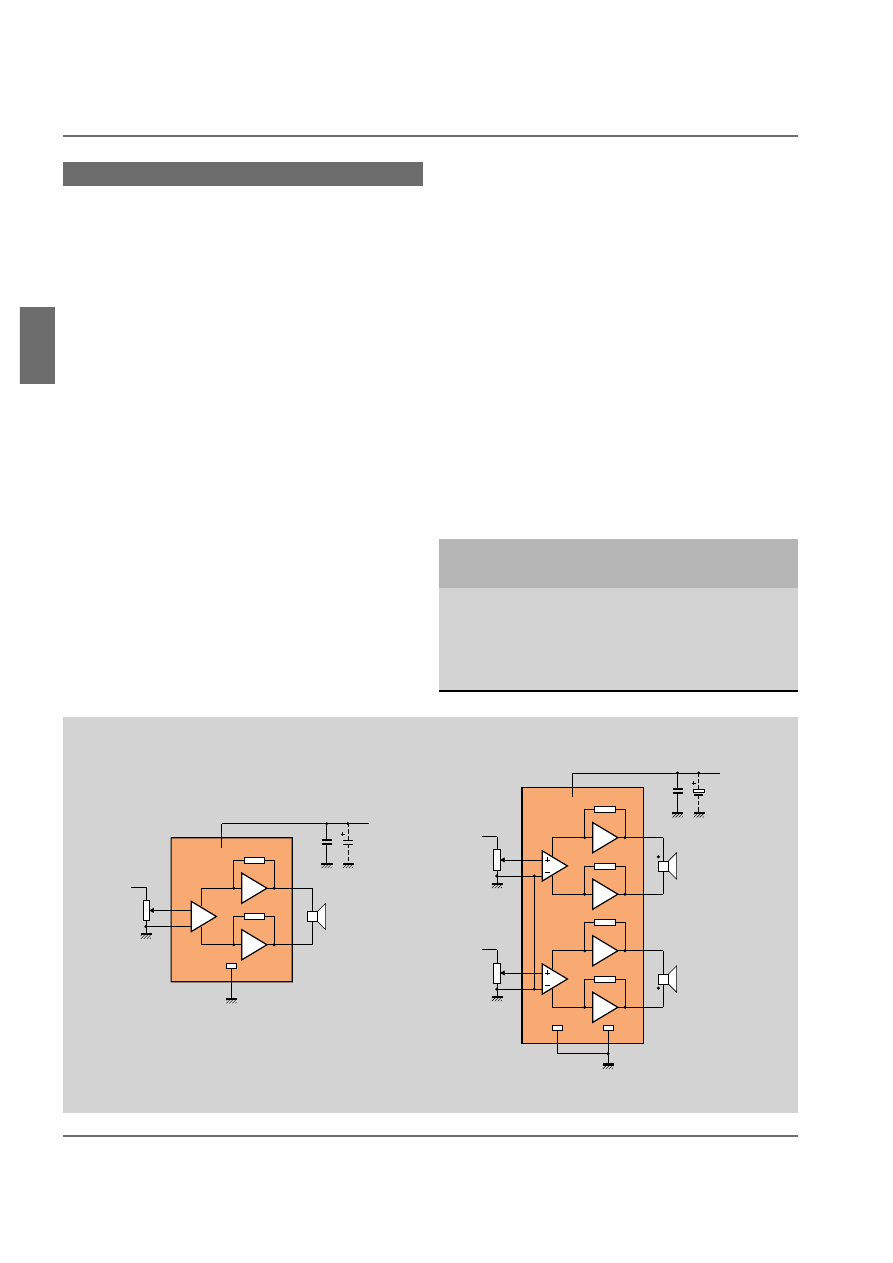
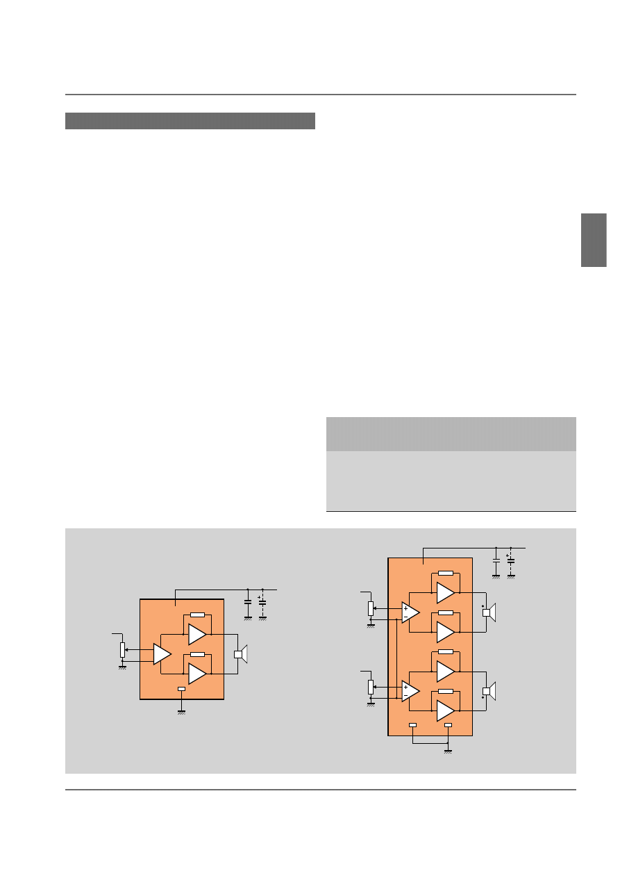
Like the TDA1510AQ/1515BQ these are car audio class-B
power amplifiers but with internally fixed gain for excellent
channel balance (within 1 dB). The three types are virtually
identical except for their gain. The TDA1516CQ is identical to
the TDA1516BQ except that it consumes very little current in
short-circuit to ground condition (typically 5.5 mA) and is only
suitable for operation in BTL mode.
The ICs come in 13-pin plastic SIL power packages with the
pins bent to DIL format.
TDA1516BQ/TDA1516CQ/TDA1518BQ in BTL mono configuration
TDA1516BQ/TDA1518BQ in single-ended stereo configuration
POWER OUTPUT AT d
tot
= 10%
power
supply
load
output
voltage
impedance
(W)
(V)
(
Ω
)
mono BTL with bootstrapping
24
14.4
4
mono BTL without bootstrapping
22
14.4
4
stereo with bootstrapping
2
×
7
14.4
4
2
×
12
14.4
2
stereo without bootstrapping
2
×
6
14.4
4
2
×
11
14.4
2
AUDIO AMPLIFIER IC
S
CAR RADIOS/POWER BOOSTERS
4-5
Audio Amplifier ICs
4
MSB261 - 1
100 nF
P
V
60 k
Ω
TDA1517
stand-by switch
220 nF
input 1
1000
µ
F
input
reference
voltage
220 nF
input 2
1000
µ
F
2200
µ
F
internal
1/2 VP
100
µ
F
60 k
Ω
TDA1517(P)/TDA1519
2
×
6 W amplifiers
■
Fixed closed-loop voltage gain of typically 20 dB for
the TDA1517(P), 40 dB for the TDA1519 (14.4 V
supply, 4
Ω
load)
■
Excellent channel balance (within 1 dB)
■
High supply voltage ripple rejection (48 dB
between 100 Hz and 10 kHz, R
s
= 0
Ω
)
■
Load dump protection
■
Output protected against AC and DC short-circuit
to ground or supply
■
Thermal and SOAR protection
■
Reverse polarity safe
■
Protected against electrostatic discharge
■
Few external components needed
■
Standby feature with switch-on voltage of 0 V to
2 V at pin 8 and a switch-on current of only 12 µA
to allow use of an inexpensive switch. The standby
supply current is <100 µA. The voltage at pin 8 for
normal operation is >8.5 V
■
Mute facility with switch-on voltage of 3 V to 6.4 V
at pin 8 to eliminate switch-on/switch-off clicks.
The supply current in the muted condition is
40 mA
POWER OUTPUT AT d
tot
= 10%
power
supply
load
output
voltage
impedance
(W)
(V)
(
Ω
)
2
×
6
14.4
4
AUDIO AMPLIFIER IC
S
CAR RADIOS/POWER BOOSTERS
The TDA1517 and TDA1519 are stereo power amplifiers devel-
oped for use in car audio systems. They are virtually identical
except for their gain.
The TDA1517 and TDA1519 come in 9-pin plastic SIL
medium-power packages and the TDA1517P comes in an
18-pin DIP.
4-6
Audio Amplifier ICs
4
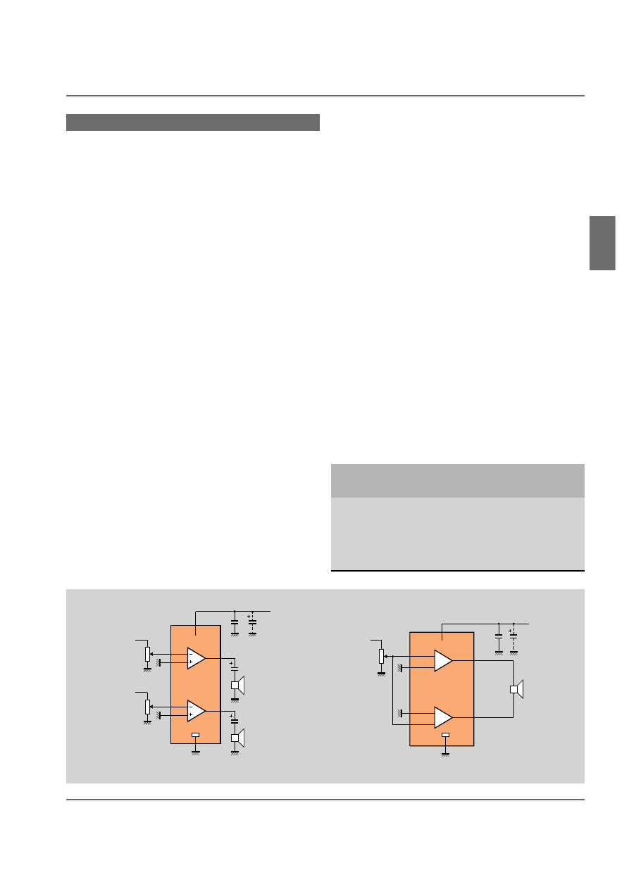
TDA1519A/TDA1519B
22 W BTL or 2
×
11 W/12 W BTL or
2
×
6 W amplifiers
■
No external components in BTL configuration
■
Very few external components in stereo
configuration
■
Low offset voltage at output (250 mV) – important
for BTL
■
Fixed closed-loop voltage gain (14.4 V supply, 4
Ω
load) of 46 dB for BTL and 40 dB for stereo
■
High supply voltage ripple rejection (48 dB
between 100 Hz and 10 kHz, R
s
= 0
Ω
)
■
Load dump protection
■
Output protected against AC and DC short-circuit
to ground or supply rail
■
Thermal protection
■
Reverse polarity safe
■
Standby feature with switch-on voltage of 0 V to
2 V at pin 8 and a switch-on current of only 12 µA
to allow use of an inexpensive switch. The standby
supply current is <100 µA. The voltage at pin 8 for
normal operation is >8.5 V
POWER OUTPUT AT d
tot
= 10%
power
supply
load
output
voltage
impedance
(W)
(V)
(
Ω
)
mono BTL (TDA1519A/1519B)
22/12
14.4
4
stereo (TDA1519A/1519B)
2
×
11/6
14.4
4
■
Mute facility with switch-on voltage of 3.3 V to
6.4 V at pin 8 to eliminate switch-on/switch-off
clicks. The supply current in the muted condition
is 40 mA
■
Identical inputs (inverting and non-inverting)
These are car audio class-B power amplifiers with internally
fixed gain for excellent channel balance (within 1 dB). The two
types are virtually identical except for their output power.
The TDA1519A comes in a 9-pin power plastic SIL package
with or without the pins bent to DIL format. The TDA1519B
comes in a 9-pin plastic medium-power SIL package.
MSB260
100 nF
2.2
mF
P
V
2
4
TDA1519A(B)
8
7
1
stand-by switch
220 nF
input 1
9
220 nF
input 2
5
60 k
Ω
6
1 mF
internal
V ref.
60 k
Ω
3
1/2 VP
100 nF
2.2
mF
P
V
2
4
TDA1519A(B)
8
7
1
stand-by switch
220 nF
input
9
5
60 k
Ω
6
internal
Vref.
3
1/2 VP
60 k
Ω
TDA1519A(B) in BTL mono configuration
TDA1519A(B) in single-ended stereo configuration
AUDIO AMPLIFIER IC
S
CAR RADIOS/POWER BOOSTERS
4-7
Audio Amplifier ICs
4
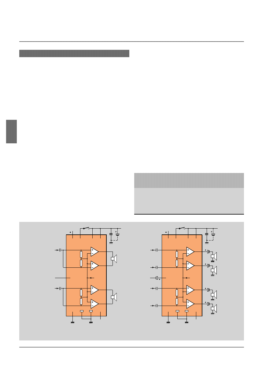
TDA1552Q/TDA1553Q/CQ/TDA1557Q
2
×
22 W BTL amplifiers
■
Very few external components
■
Low offset voltage at output (150 mV; 250 mV for
the TDA1557Q) – important for BTL
■
Fixed closed-loop voltage gain (14.4 V supply, 4
Ω
load) of 26 dB (46 dB for the TDA1557Q)
■
High supply voltage ripple rejection (48 dB
between 100 Hz and 10 kHz, R
s
= 0
Ω
)
■
Load dump protection
■
Output protected against AC and DC short-circuit
to ground or supply rail
■
Low current consumption in short-circuit to
ground condition (typ. 5.5 mA)
■
Thermal protection
■
Reverse polarity safe
■
Standby feature with switch-on voltage of 0 V to
2 V at pin 11 and a switch-on current of only 25 µA
to allow use of an inexpensive switch. The standby
supply current is <100 µA. The voltage at pin 11
for normal operation is >8.5 V
■
Mute facility with switch-on voltage of 3.3 V to
6.4 V at pin 11 to eliminate switch-on/switch-off
clicks
■
TDA1553CQ incorporates mute/standby/normal
operation selection with CMOS-compatible switch-
ing levels
■
Loudspeaker protection limits voltage across the
associated loudspeaker to 1 V or less in the event
any of the outputs being short-circuited to ground
(TDA1553Q, TDA1553CQ and TDA1557Q)
These are car audio class-B power amplifiers with internally
fixed gain for excellent channel balance (within 1 dB). The four
types are virtually identical except that the TDA1553Q,
TDA1553CQ and TDA1557Q incorporate loudspeaker protec-
tion and that the TDA1557Q has a 20 dB higher gain.
They come in 13-pin plastic SIL power packages with the pins
bent to DIL format.
POWER OUTPUT AT d
tot
= 10%
power
supply
load
output
voltage
impedance
(W)
(V)
(
Ω
)
2
×
22
14.4
4
100 nF
2.2
mF
P
V
5
signal ground
power ground (substrate)
4
6
60 k
Ω
12
not connected
TDA1552Q/TDA1557Q
11
3
10
1
mute/stand-by
2
V ref
220 nF
input 1
9
7
13
220 nF
input 2
8
60 k
Ω
MSB257
100 nF
2.2
mF
P
V
5
signal ground
power ground (substrate)
4
6
12
TDA1553Q(CQ)
11
3
10
1
mute/stand-by
2
V ref
220 nF
input 1
9
7
13
220 nF
input 2
8
60 k
Ω
60 k
Ω
TDA1552Q/TDA1557Q in BTL stereo configuration
TDA1553Q/TDA1553CQ in BTL stereo configuration
AUDIO AMPLIFIER IC
S
CAR RADIOS/POWER BOOSTERS
* connected to V
ref
on
the TDA1557Q
4-8
Audio Amplifier ICs
4
TDA1554Q/TDA1555Q/TDA1558Q
2
×
22 W BTL or 4
×
11 W amplifiers
■
Very few external components
■
Low offset voltage at output (100 mV, 250 mV for
the TDA1558Q) – important for BTL
■
Fixed closed-loop voltage gain (14.4 V supply, 4
Ω
load) of 20 dB (26 dB in BTL), 40 dB (46 dB in
BTL) for the TDA1558Q
■
High supply voltage ripple rejection (48 dB
between 100 Hz and 10 kHz, R
s
= 0
Ω
)
■
Load dump protection
■
Output protected against AC and DC short-circuit
to ground or supply rail
■
Thermal protection
■
Reverse polarity safe
■
Standby feature with switch-on voltage of 0 V to
2 V at pin 14 and a switch-on current of only 12 µA
to allow use of an inexpensive-pensive switch. The
standby supply current is >100 µA. The voltage at
pin 14 for normal operation is >8.5 V
■
Mute facility with switch-on voltage of 3.3 V to
6.4 V at pin 14 to eliminate switch-on/switch-off
clicks
■
Identical inputs (inverting and non-inverting)
■
Distortion detector senses output clipping and for
clip distortion of 3.5% it supplies a current of
50 µA typical for reducing the drive via a sound
processor or DC volume control (TDA1555Q only)
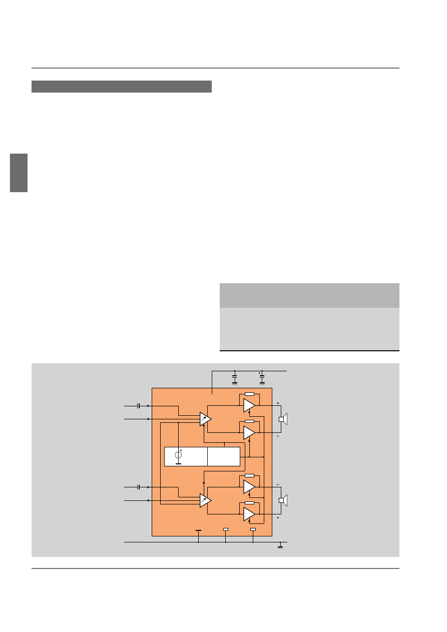
These are class-B power amplifiers with internally fixed gain for
excellent channel balance (within 1 dB). They are for BTL
stereo or quad (front and rear stereo) car audio applications. The
three types are virtually identical except that the TDA1555Q
incorporates distortion detection, and the TDA1558Q has
20 dB higher gain.
They come in 17-pin plastic SIL power packages with the pins
bent to DIL format.
POWER OUTPUT AT d
tot
= 10%
power
supply
load
output
voltage
impedance
(W)
(V)
(
Ω
)
BTL stereo
2
×
22
14.4
4
quad
4
×
11
14.4
2
4
×
6
14.4
4
9
MSB255
100 nF
2.2
mF
P
V
7
signal ground
power ground (substrate)
1 mF
1 mF
6
8
60 k
Ω
15
distortion detector
TDA1554Q/1555Q/1558Q
14
5
13
1
2
mute/stand-by switch
4
V /2
P
V ref
220 nF
220 nF
input 1
input 2
100
µ
F
supply
ripple
rejection
1 mF
1 mF
12
10
60 k
Ω
17
16
220 nF
220 nF
input 3
input 4
11
3
9
100 nF
2.2
mF
P
V
7
signal ground
power ground (substrate)
6
8
60 k
Ω
15
distortion detector
TDA1554Q/1555Q/1558Q
14
5
13
1
2
mute/stand-by switch
4
V /2
P
V ref
220 nF
input 1
supply
ripple
rejection
12
10
60 k
Ω
17
16
220 nF
input 2
11
3
not connected
not connected
60 k
Ω
60 k
Ω
60 k
Ω
60 k
Ω
TDA1554Q/TDA1555Q/TDA1558Q in BTL stereo configuration
TDA1554Q/TDA1555Q/TDA1558Q in single-ended quad (dual stereo)
configuration
AUDIO AMPLIFIER IC
S
CAR RADIOS/POWER BOOSTERS
* not connected
on the TDA1554Q
connected to V
ref
on the TDA1558Q
4-9
Audio Amplifier ICs
4
TDA1556Q
2
×
22 W BTL amplifier with differential
inputs
■
Very few external components
■
Differential inputs
■
High CMRR (>64 dB)
■
High supply voltage ripple rejection (48 dB
between 100 Hz and 10 kHz, R
s
= 0
Ω
)
■
Low offset voltage at output (150 mV) – important
for BTL
■
Fixed closed-loop voltage gain (14.4 V supply, 4
Ω
load) of 26 dB
■
Load dump protection
■
Thermal protection
■
Outputs protected against AC and DC short-
circuit to ground, supply rail or across load
■
Low current consumption in short-circuit to
ground condition (5.5 mA)
■
Reverse polarity safe
■
Loudspeaker protection limits voltage across the
associated loudspeaker to 1 V or less in the event
any of the outputs being short-circuited to ground
■
Standby feature with switch-on voltage of 0 V to
2 V at pin 14 and a switch-on current of only 25 µA
to allow use of an inexpensive switch. The standby
supply current is <100 µA. The voltage at pin 14
for normal operation is >8.5 V
■
Mute facility with switch-on voltage of 3.3 V to
6.4 V at pin 14 to eliminate switch-on/switch-off
clicks
■
Distortion detector senses output clipping. It pro-
vides 50 µA typical for a clip distortion of 3.5% to
reduce input drive via a sound processor or DC
volume control
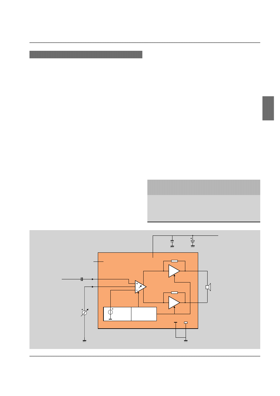
This is a class-B power amplifier with internally fixed gain for
excellent channel balance (within 1 dB). The amplifier has two
differential input stages with high Common Mode Ripple
Rejection (CMRR) which makes it very attractive for car radio
booster applications. The TDA1556Q also incorporates a
Dynamic Distortion Detector (DDD) and loudspeaker protec-
tion.
It comes in a 17-pin plastic SIL power package with the pins
bent to DIL format.
POWER OUTPUT AT d
tot
= 10%
power
supply
load
output
voltage
impedance
(W)
(V)
(
Ω
)
2
×
22
14.4
4
15
Vref
9
3
n.c.
n.c.
7
11
MBC271
TDA1556Q
100
nF
DDD
on/mute/stand-by
4
14
5
13
VP
2200
µ
F
4.7
µ
F
220 nF
220 nF
16
17
10
12
220 nF
220 nF
1
2
6
8
input 1
input 2
input 3
input 4
60 k
Ω
60 k
Ω
60 k
Ω
60 k
Ω
AUDIO AMPLIFIER IC
S
CAR RADIOS/POWER BOOSTERS
TDA1556Q in BTL stereo configuration
4-10
Audio Amplifier ICs
4
TDA1560Q
40 W BTL class-H amplifier
■
Few external components
■
Very high output power
■
Low power dissipation when reproducing music
■
Fixed closed-loop voltage gain (14.4 V supply, 8
Ω
load) of 30 dB
■
High supply voltage ripple rejection of 55 dB over
the frequency range 100 Hz to 10 kHz, R
s
= 0
Ω
)
■
Switches to low output power if the heatsink over-
heats
■
Low crossover distortion
■
No switch-on/off clicks
■
Thermal protection
■
Mode switch for standby (0 to 1.2 V)/mute (2.6 to
3.5 V)/class-B (4.5 to 7 V)/class-H (8.5 V to V
p
)
operation. Maximum switch current is only 20 µA
to allow use of an inexpensive-pensive switch
■
Low offset voltage at the output – important for
BTL
■
Load dump protection
■
Load short-circuit safe to ground or V
p
■
Pins protected against ESD
■
Thermal protection
Primarily for car audio applications, this IC uses class-H amplifi-
er techniques so that, with a 14.4 V supply and minimal
heatsinking, it can deliver 40 W into an 8
Ω
load. For the first
time, this allows a 4
×
40 W car radio to be assembled in a stan-
dard DIN-sized car radio case.
Below 10 W the IC acts as a normal BTL amplifier. At higher
outputs, the internal supply voltage is doubled by adding the
charge stored on external capacitors. This allows the power out-
put to increase to 40 W.
The amplifier comes in a 17-pin plastic SIL power package with
the pins bent to DIL format.
SUPPLY
SUPPLY
TEMPERATURE
SENSOR
INPUT AND
FEEDBACK
CIRCUIT
13
10
2200 F
100 nF
2200 F
ground
9
MCD333 - 3
output 2 (+)
voltage
reference
V
POWER
STAGE
POWER
STAGE
5
8
2200 F
7
11
1
0.22 F
1
0.22 F
0.22 F
15
mode select switch
16
150
k
1
Ck
Ck
S1
2
4
R = 100 k
ex
150 nF
150 nF
input (+)
input
input (–)
output 1 (–)
15 k
10 F
10 k
17
disable
disable
VP
VP
12
6
Vref
TDA1560Q
Ω
Ω
µ
2
0.22 F
µ
Ω
µ
µ
µ
Ω
Ω
150
k
Ω
µ
Ω
Ω
µ
µ
3
µ
2
0.22 F
Ω
P
LOAD DUMP
TEMPERATURE
AND CURRENT
PROTECTION
14
diagnostic
output
POWER OUTPUT AT d
tot
= 10%
power
supply
load
output
voltage
impedance
(W)
(V)
(
Ω
)
17
14.4
4
40
14.4
8
AUDIO AMPLIFIER IC
S
CAR RADIOS/POWER BOOSTERS
4-11
Audio Amplifier ICs
4
TDA1561Q
2
×
23 W high efficiency power amplifier
■
Low power dissipation since the amplifier switches
from SE mode into BTL mode only when receiving
high-amplitude signals
■
High common-mode rejection ratio
■
Mute/standby/BTL-disable switch (mode select pin)
■
Zero-crossing mute
■
Load dump protection
■
Short-circuit safe to ground, V
p
and across load
■
Loudspeaker protection
■
Automatically switches to SE mode at excessive
crystal temperature
■
Thermal protection
This power amplifier normally operates in low-power single-
ended mode and switches to high-power BTL mode only when
large amplitude signals are received from the preamplifer. The
TDA1561Q therefore dissipates only about 55% of the power
dissipated by a conventional power amplifier (measured at aver-
age maximum music power) which means heatsinks can be
smaller. Primarily for car audio applications, the amplifier is also
ideal for multimedia systems and active loudspeakers.
The TDA1561Q comes in a 13-pin plastic SIL power package
with the pins bent to DIL format.
MLD214
REFERENCE
SOURCES
MUTE/STANDBY
THERMAL/
SHORT-CIRCUIT
PROTECTION
HIGHER
TEMPERATURE
BTL DISABLE
0.5VP
MUTE
R
MUTE
R
7
VP
12
3
13
2
1
IN1
IN2
CIN
MODE
1/2R
HV
4
GND1
10
GND2
6
5
11
9
8
OUT2
OUT2
OUT1
OUT1
C
TDA1561Q
P
11
POWER OUTPUT AT d
tot
= 10%
power
supply
load
output
voltage
impedance
(W)
(V)
(
Ω
)
2
×
23
14.4
4
AUDIO AMPLIFIER IC
S
CAR RADIOS/POWER BOOSTERS
4-12
Audio Amplifier ICs
4
TDA8560Q/TDA8563Q/TDA8563AQ
2
×
40 W BTL amplifiers
■
Very few external components
■
High supply voltage ripple rejection (>50 dB
between 100 Hz and 10 kHz, R
s
= 0
Ω
)
■
Low offset voltage (150 mV) at output (200 mV for
TDA8560Q) – important for BTL
■
Fixed closed-loop voltage gain (14.4 V supply, 4
Ω
load) of 26 dB (TDA8563Q/TDA8563AQ) or 40 dB
(TDA8560Q)
■
Load dump protection
■
Thermal protection
■
Outputs protected against AC and DC short-
circuit to ground, supply rail or across load
■
Low current consumption in short-circuit to
ground condition
■
Reverse polarity safe
■
Standby feature with switch-on voltage of 0 V to
2 V at pin 11 and a switch-on current of only 15 µA
to allow use of an inexpensive switch. The standby
supply current is <100 µA. The voltage at pin 11
for normal operation is >8.5 V
■
Mute facility with switch-on voltage of 3.3 V to
6.4 V at pin 11 to eliminate switch-on/switch-off
clicks
■
Diagnostic facility senses distortion, load short-
circuit and temperature
■
Pins protected against ESD
■
Low thermal resistance
These are class-B power amplifiers with internally-fixed voltage
gain for excellent channel balance (within 1 dB). They are pri-
marily for car audio applications. The amplifiers are distinguish-
able by their closed-loop voltage gain. The gain of the
TDA8560Q is 40 dB, and that of the TDA8563Q and
TDA8563AQ is 26 dB.
A diagnostic facility senses distortion, load short-circuit and
temperature. At onset of distortion (10% THD in the
TDA8560Q/TDA8663Q, 2.5% THD in the TDA8563AQ) or
temperature >150 °C, the diagnostic output signal can be used
to reduce the input drive via a sound processor or DC volume
control. For load short-circuit or output short-circuit to ground
or supply, the outputs are switched-off until the short-circuit is
removed.
The ampliers come in 13-pin plastic SIL power packages with
the pins bent to DIL format.
POWER OUTPUT AT d
tot
= 10%
power
supply
load
output
voltage
impedance
(W)
(V)
(
Ω
)
2
×
21
13.2
4
2
×
25
14.4
4
2
×
35
13.2
2
2
×
40
14.4
2
MLB666 - 2
100
nF
mode switch
11
3
10
470 nF
1
4
6
470 nF
13
9
7
5
8
VP
TDA8560Q
TDA8563Q
2200
µ
F
30
k
Ω
reference
voltage
2
ground (signal)
30
k
Ω
input 2
input 1
power ground (substrate)
12
10 k
Ω
VP
diagnostic
output
AUDIO AMPLIFIER IC
S
CAR RADIOS/POWER BOOSTERS
4-13
Audio Amplifier ICs
4
TDA8561Q/TDA8564Q
2
×
24 W BTL or 4
×
12 W amplifiers
■
Very few external components
■
Low offset voltage (150 mV) at output (250 mV for
TDA8564Q) – important for BTL
■
High supply voltage ripple rejection (>48 dB
between 100 Hz and 10 kHz, R
s
= 0
Ω
)
■
Load dump protection
■
Output protected against AC and DC short-circuit
to ground or supply rail
■
Low current consumption (40 mA) during any
short-circuit condition
■
Thermal protection
■
Reverse polarity safe
■
Standby feature with switch-on voltage of 0 V to
2 V at pin 14 and a switch-on current of only 12 µA
to allow use of an inexpensive-pensive switch. The
standby supply current is >100 µA. The voltage at
pin 14 for normal operation is >8.5 V
■
Mute facility with switch-on voltage of 3.3 V to 6.4 V
at pin 14 to eliminate switch-on/switch-off clicks
■
Identical inputs (inverting and non-inverting)
■
Diagnostic facility senses distortion, load short-
circuit and temperature
■
Pins protected against ESD
■
Low thermal resistance
These are class-B power amplifiers with internally-fixed gain for
excellent channel balance (within 1 dB). They are for BTL
stereo or quad (front and rear stereo) car audio applications. The
two types are identical except that the TDA8561Q has a fixed
closed-loop voltage gain of 26 dB (BTL)/20 dB (single-ended)
whereas that of the TDA8564Q 46 dB (BTL) and 40 dB
(single-ended).
A diagnostic facility senses distortion, load short-circuit and
temperature. At onset of distortion or temperature >150 °C, the
diagnostic output signal can be used to reduce the input drive
via a sound processor or DC volume control. For load short-
circuit or output short-circuit to ground or supply, the outputs
are switched-off until the short-circuit is removed.
The amplifiers come in 17-pin plastic SIL power packages with
the pins bent to DIL format.
POWER OUTPUT AT d
tot
= 10%
power
supply
load
output
voltage
impedance
(W)
(V)
(
Ω
)
BTL stereo
2
×
24
14.4
4
quad
4
×
7
14.4
4
4
×
12
14.4
2
MEA862 - 2
100
nF
16
5
13
220 nF
1
6
8
7
11
VP
TDA8561Q
TDA8564Q
2200
µ
F
60
k
Ω
2
ground (signal)
10
k
Ω
14
9
not connected
3
inverting input 2
60
k
Ω
60
k
Ω
reference
voltage
220 nF
17
12
60
k
Ω
non-inverting
input 4
4
15
10
power ground (substrate)
non- inverting
input 1
supply voltage
ripple rejection
inverting input 3
diagnostic
mode
switch
MEA863 - 2
100
nF
16
5
13
220 nF
1
6
8
7
11
VP
TDA8561Q
TDA8564Q
2200
µ
F
60
k
Ω
2
ground (signal)
10
k
Ω
14
9
not connected
3
inverting
input 2
60
k
Ω
60
k
Ω
reference
voltage
220 nF
17
12
60
k
Ω
non-inverting
input 4
4
15
10
power ground (substrate)
non- inverting
input 1
supply voltage
ripple rejection
inverting
input 3
220 nF
1/2Vp
1000
µ
F
220 nF
1000
µ
F
1000
µ
F
1000
µ
F
mode
switch
TDA8561Q/TDA8564Q in BTL stereo configuration left, and in single-ended quad (front and rear stereo) configuration
AUDIO AMPLIFIER IC
S
CAR RADIOS/POWER BOOSTERS
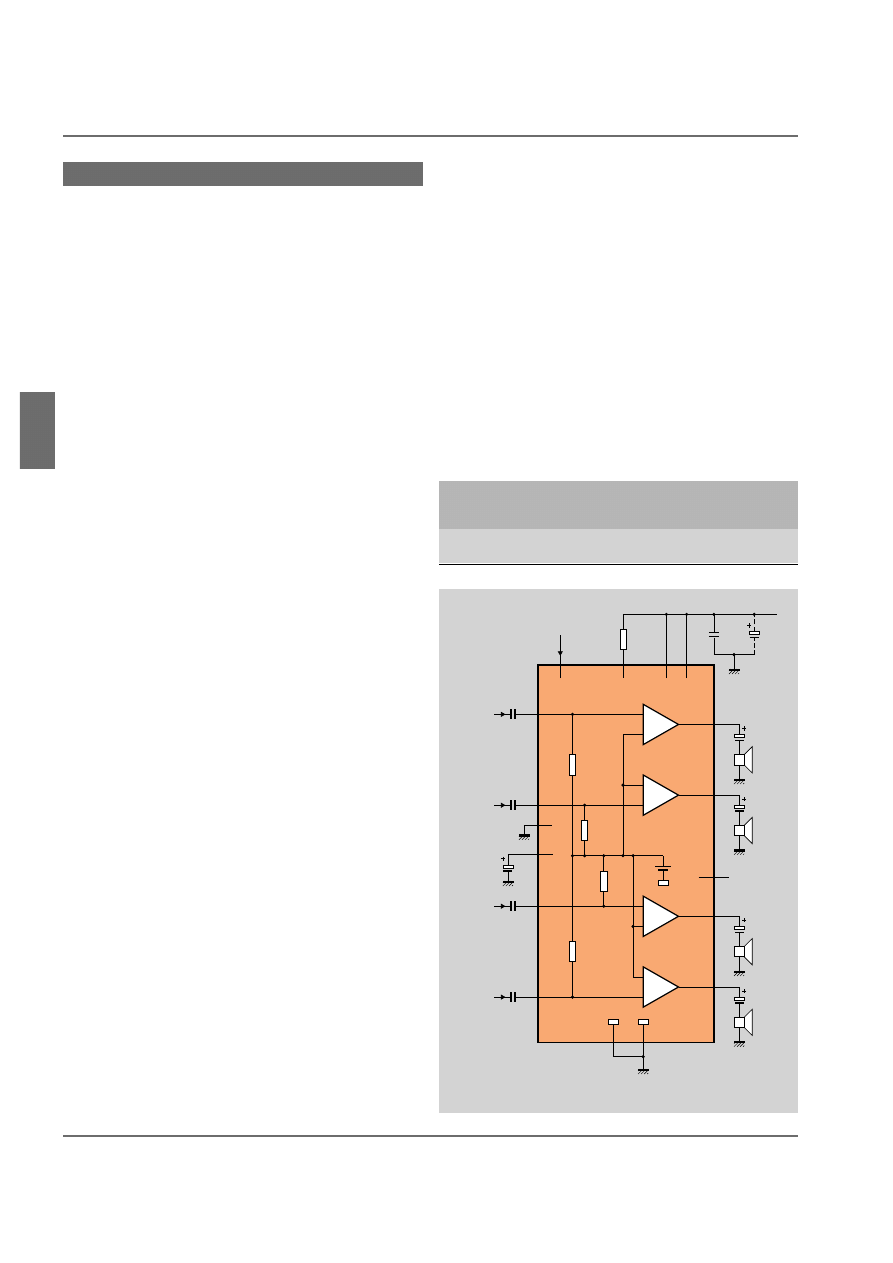
4-14
Audio Amplifier ICs
4
TDA8562Q/TDA8565Q
4
×
12 W single-ended amplifier
■
Very few external components
■
High supply voltage ripple rejection (>48 dB
between 100 Hz and 10 kHz, R
s
= 0
Ω
)
■
Load dump protection
■
Output protected against AC and DC short-circuit
to ground or supply rail
■
Low current consumption (40 mA) during any
short-circuit condition
■
Identical inputs
■
Thermal protection
■
Reverse polarity safe
■
Standby feature with switch-on voltage of 0 V to
2 V at pin 8 and a switch-on current of only 12 µA
to allow use of an inexpensive switch. The standby
supply current is <100 µA. The voltage at pin 8 for
normal operation is >8.5 V
■
Mute facility to eliminate switch-on/switch-off
clicks
■
Diagnostic facility for sensing distortion, short-
circuit and temperature
■
Pins protected against ESD
■
Low thermal resistance
These are car audio class-B power amplifiers with internally
fixed gain for excellent channel balance (within 1 dB). They are
for quad (front and rear stereo) car audio applications. The two
types are identical except that the TDA8562Q has a fixed
closed-loop voltage gain of 20 dB, whilst that of the
TDA8565Q is 20 dB higher.
A diagnostic facility senses distortion, load short-circuit and
temperature. At onset of distortion or temperature >150 °C, the
diagnostic output signal can be used to reduce the input drive
via a sound processor or DC volume control. For load short-
circuit or output short-circuit to ground or supply, the outputs
are switched-off until the short-circuit is removed
The amplifiers come in 17-pin plastic SIL power packages with
the pins bent to DIL format.
MEA867 - 2
100
nF
16
5
13
220 nF
1
6
8
7
11
VP
TDA8562Q
TDA8565Q
2200
µ
F
60
k
Ω
2
ground (signal)
10
k
Ω
9
not connected
3
input 2
60
k
Ω
60
k
Ω
reference
voltage
220 nF
17
12
60
k
Ω
input 4
4
15
10
power ground (substrate)
input 1
supply
voltage
ripple
rejection
input 3
220 nF
V /2
p
1000
µ
F
220 nF
100
µ
F
14
diagnostic
1000
µ
F
1000
µ
F
1000
µ
F
mode
switch
POWER OUTPUT AT d
tot
= 10%
power
supply
load
output
voltage
impedance
(W)
(V)
(
Ω
)
4
×
7
14.4
4
4
×
12
14.4
2
AUDIO AMPLIFIER IC
S
CAR RADIOS/POWER BOOSTERS
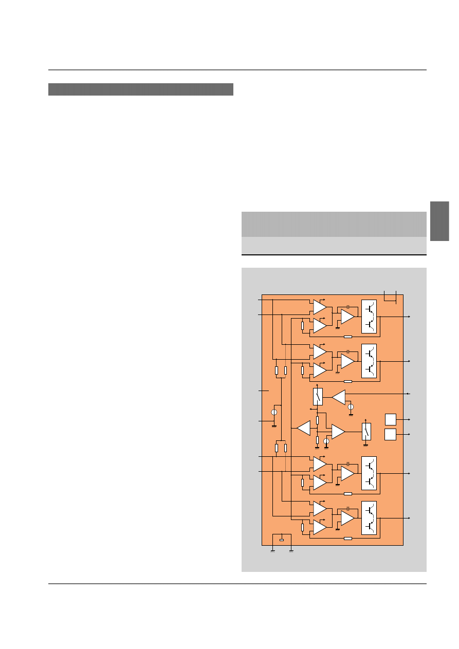
4-15
Audio Amplifier ICs
4
TDA8566Q
2
×
25 W BTL power amplifier with
differential inputs
■
Differential inputs
■
Very high Common Mode Rejection Ratio
■
High common mode input signal handling capacity
■
Very few external components
■
High output power
■
Low offset voltage at output (<100 mV) –
important for BTL
■
Fixed gain
■
Diagnostic facility for sensing distortion, short-
circuit and temperature
■
Good ripple rejection
■
Mode-select switch (operating, mute and standby)
■
Load dump protection
■
Short-circuit proof to ground, to V
p
and across the
load
■
Low power dissipation in any short circuit
condition
■
Thermally protected
■
Reverse-polarity safe
■
Pins protected against ESD
■
No switch-on/switch-off clicks
■
Low thermal resistance
This is a class-B BTL stereo power amplifier. It features a high-
impedance fully-differential balanced input stage that’s also
capable of operating in single-ended mode (with one input
capacitively coupled to an audio ground).
A diagnostic facility senses distortion, load short-circuit and
temperature. At onset of distortion or temperature >145 °C, the
diagnostic output signal can be used to reduce the input drive
via a sound processor or DC volume control. For load short-cir-
cuit or output short-circuit to ground or supply, the outputs are
switched-off until the short-circuit is removed.
The amplifier comes in 17-pin plastic SIL power package with
the pins bent to DIL format.
POWER OUTPUT AT d
tot
= 10%
power
supply
load
output
voltage
impedance
(W)
(V)
(
Ω
)
2
×
25
14.4
4
2
×
40
14.4
2
+
−
+
−
CM
VA
(9
×
)
2.3 k
Ω
2.3
k
Ω
mute
switch
+
−
+
−
CM
VA
VA
1
×
standby
reference
voltage
standby
switch
mute
reference
voltage
Vref
mute
switch
CLIP
(9
×
)
2.3 k
Ω
2.3
k
Ω
60
k
Ω
60
k
Ω
60
k
Ω
60
k
Ω
mute
switch
+
−
+
−
CM
VA
(9
×
)
2.3 k
Ω
2.3
k
Ω
mute
switch
+
−
+
−
CM
VA
11
7
12
10
15
4
TDA8566Q
14
8
6
13
5
1
2
3
16
17
VP2
VP1
PGND2
PGND1
OUT2
−
OUT2
+
OUT1
−
OUT1
+
IN1
−
IN1
+
IN2
−
IN2
+
SGND
n.c.
DIAG
MODE
CLIP
MGD105
(9
×
)
2.3 k
Ω
2.3
k
Ω
mute
switch
9
DIAG
AUDIO AMPLIFIER IC
S
CAR RADIOS/POWER BOOSTERS
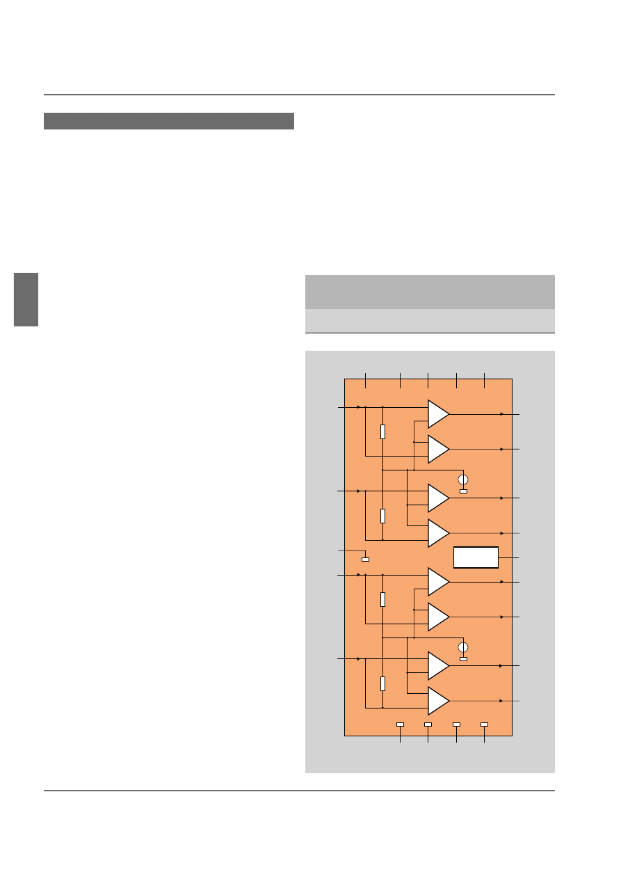
4-16
Audio Amplifier ICs
4
TDA8567Q/TDA8568Q/TDA8569Q
4
×
25 W BTL amplifiers
■
Very few external components
■
High output power
■
Low offset voltage at output (TDA8567Q &
TDA8569Q < 150 mV, TDA8568Q < 200 mV) –
important for BTL
■
Diagnostic facility for sensing distortion, short-
circuit and temperature
■
Good ripple rejection
■
Mode-select switch (operating, mute and standby)
■
Load dump protection
■
Short-circuit proof to ground, to V
p
and across the
load
■
Low power dissipation in any short circuit
condition
■
Thermally protected
■
Reverse-polarity safe
■
Pins protected against ESD
■
No switch-on/switch-off clicks
■
Low thermal resistance
These are class-B power amplifiers with internally fixed gain for
excellent channel balance. They are for quad (front and rear
stereo) car audio applications. The TDA8567Q and
TDA8569Q have a fixed closed-loop voltage gain of 26 dB,
whilst that of the TDA8568Q is 40 dB. The TDA8569, more-
over, can drive loads down to 2
Ω
.
A diagnostic facility senses distortion, load short-circuit and
temperature. At onset of distortion or temperature >145 °C, the
diagnostic output signal can be used to reduce the input drive
via a sound processor or DC volume control. For load short-
circuit or output short-circuit to ground or supply, the outputs
are switched-off until the short-circuit is removed
The amplifiers come in 23-pin plastic SIL power packages with
the pins bent to DIL format.
POWER OUTPUT AT d
tot
= 10%
power
supply
load
output
voltage
impedance
(W)
(V)
(
Ω
)
TDA8567Q/TDA8568Q/TDA8569Q
4
×
25
14.4
4
VDIAG
DIAGNOSTIC
9
MSC264
OUT1
+
OUT1
−
+
−
+
−
Vref
2
IN1
IN2
4
23
16
8
1
15
10
MODE
VP1
VP2
VP3
VP4
21
18
6
3
PGND1
PGND2
PGND3
PGND4
30 k
Ω
OUT2
+
OUT2
−
+
−
+
−
7
5
11
30 k
Ω
OUT3
+
OUT3
−
+
−
+
−
Vref
17
IN3
SGND
TDA8567Q/
TDA8568Q/
TDA8569Q
IN4
19
13
12
30 k
Ω
OUT4
+
OUT4
−
+
−
+
−
22
20
14
30 k
Ω
AUDIO AMPLIFIER IC
S
CAR RADIOS/POWER BOOSTERS
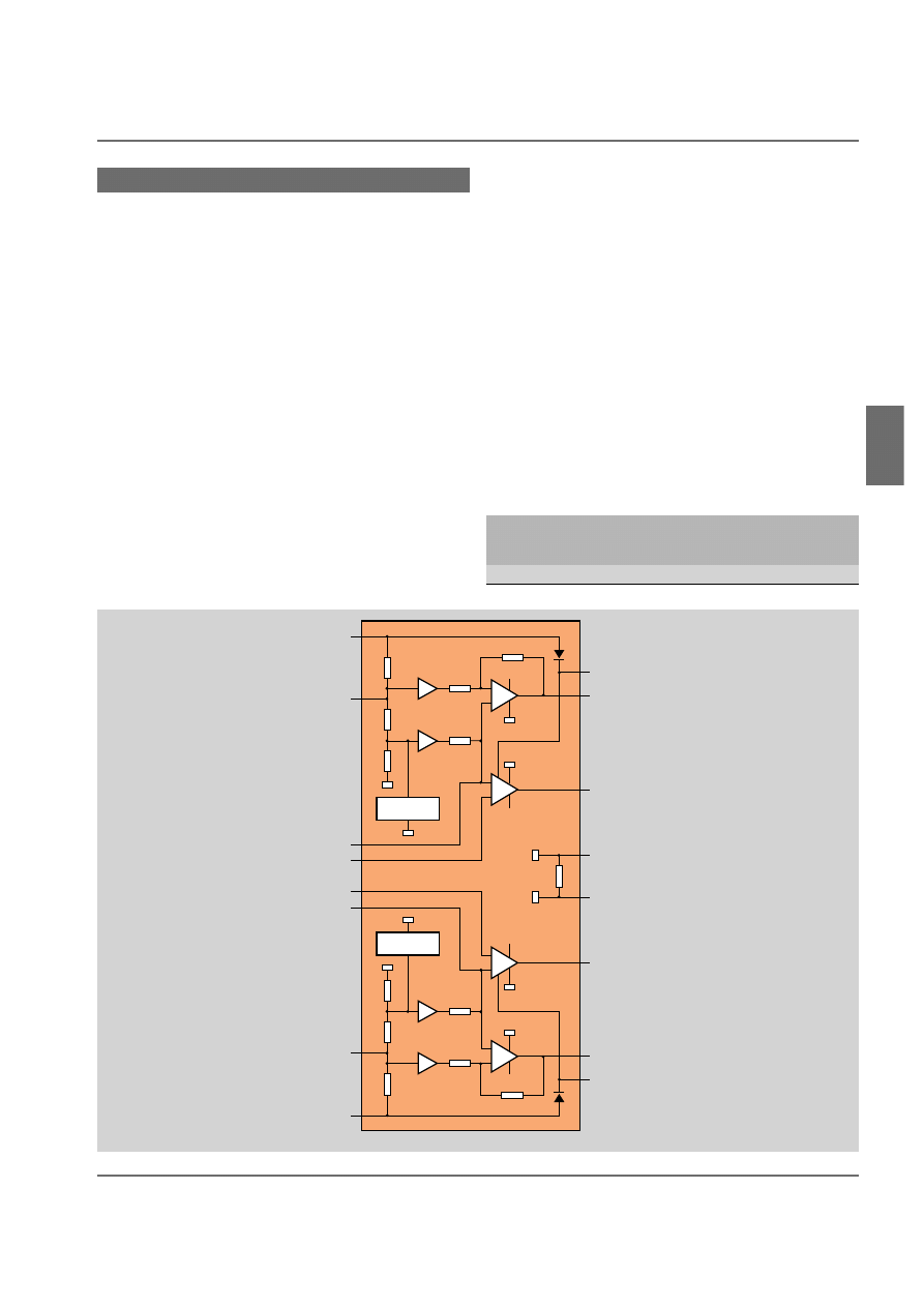
4-17
Audio Amplifier ICs
4
TDA8574(T)
Dual common-mode rejection differential
line drivers
■
Class-H operation means that output voltage
swings are greater than the supply voltage
■
High supply voltage ripple rejection
■
Low distortion (0.003% THD at 1 kHz with
V
o(rms)
= 3 V)
■
Low noise (noise output of typ. 5 µV)
■
Supply voltage range of 6 V to 12 V
■
All pins ESD protected
These two-channel class-H amplifiers with single-ended outputs
offer 8 dB voltage gain and low distortion. They’re principally
for eliminating ground noise in car and mains-powered applica-
tions with long connections between the signal sources and out-
put amplifiers (or boosters). Class-H operation ensures that volt-
age swings over the load are greater than the supply voltage: with
a supply voltage of 9 V, the output voltage swing across the load
POWER OUTPUT AT d
tot
= 0.1%
AC
supply
load
output
voltage
impedance
(V
rms
)
(V)
(
Ω
)
5
9
10 k
MGE668
24 k
Ω
30 k
Ω
5
Ω
36 k
Ω
36 k
Ω
30 k
Ω
24 k
Ω
REFERENCE
REFERENCE
LIFT
AMP.
LIFT
AMP.
SIGNAL
AMP.
SIGNAL
AMP.
TDA8574(T)
VCCL
VCCL
VCCR
VCCR
VCCL
VCCR
3
1
BUFFER
BUFFER
BUFFER
BUFFER
CL
+
CL
−
CR
+
CR
−
OUTL
13
14
11
12
10
9
6
INR
INMR
INML
INL
SVRL
8
15
16
LGND
RGND
OUTR
2
4
5
7
SVRR
+
+
−
+
−
−
+
−
AUDIO AMPLIFIER IC
S
CAR RADIOS/POWER BOOSTERS
is 14 V (peak-to-peak). This high output level significantly
improves signal-to-noise ratio of the power amplifier stage by
allowing it to operate at lower gain.
The TDA8574 comes in a 16-pin plastic DIP and the
TDA8574T comes in a 16-pin SO package for surface mount-
ing.
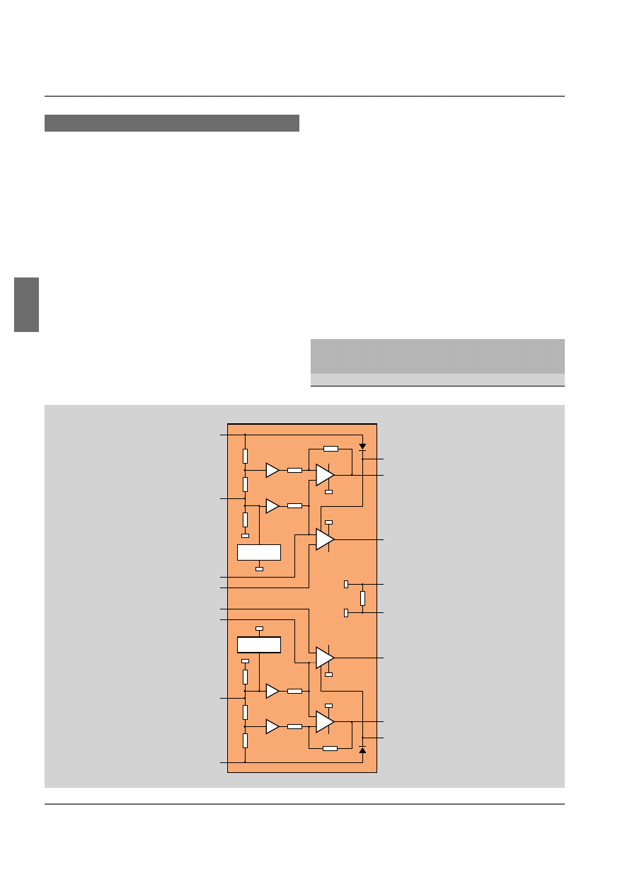
4-18
Audio Amplifier ICs
4
TDA8576T
Dual common-mode rejection differential
line driver
■
Class-H operation means that output voltage
swings are greater than the supply voltage
■
High supply voltage ripple rejection
■
Low distortion (0.005% THD at 1 kHz with
V
o(rms)
= 3 V)
■
Low noise (noise output of typ. 5 µV)
■
Supply voltage range of 6 V to 12 V
■
All pins ESD protected
This two-channel class-H amplifier with single-ended outputs
offers 6 dB voltage gain and low distortion. It’s principally for
eliminating ground noise in car and mains-powered applications
with long connections between the signal sources and output
amplifiers (or boosters). Class-H operation ensures that voltage
POWER OUTPUT AT d
tot
= 0.1%
AC
supply
load
output
voltage
impedance
(V
rms
)
(V)
(
Ω
)
5
9
10 k
MGE671
36 k
Ω
20 k
Ω
5
Ω
36 k
Ω
36 k
Ω
20 k
Ω
36 k
Ω
REFERENCE
REFERENCE
LIFT
AMP.
LIFT
AMP.
SIGNAL
AMP.
SIGNAL
AMP.
TDA8576T
VCCL
VCCL
VCCR
VCCR
VCCL
VCCR
1
BUFFER
BUFFER
BUFFER
BUFFER
CL
+
CL
−
CR
+
CR
−
OUTL
13
14
11
12
10
9
INR
INMR
INML
INL
3
SVRL
8
15
16
LGND
RGND
OUTR
2
4
5
7
6
SVRR
+
+
−
+
−
−
+
−
AUDIO AMPLIFIER IC
S
CAR RADIOS/POWER BOOSTERS
swings over the load are greater than the supply voltage: with a
supply voltage of 9 V, the output voltage swing across the load is
14 V (peak-to-peak). This high output level significantly
improves signal-to-noise ratio of the power amplifier stage by
allowing it to operate at lower gain.
The TDA8576T comes in a 16-pin SO package for surface
mounting.
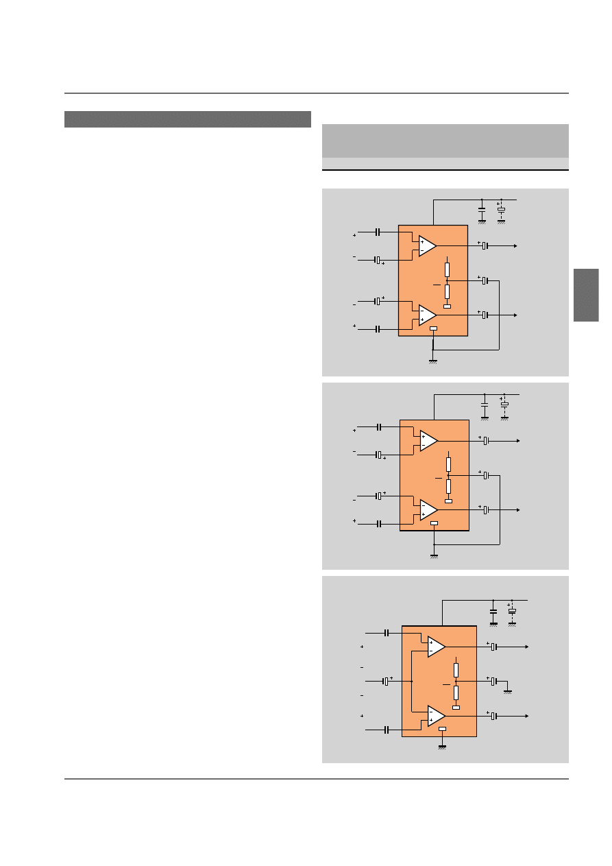
4-19
Audio Amplifier ICs
4
AUDIO AMPLIFIER IC
S
CAR RADIOS/POWER BOOSTERS
TDA8577/TDA8578(T)/TDA8579(T)
Dual common-mode rejection differential
line drivers
■
70 dB common-mode rejection from 100 Hz to
100 kHz with a 5 k
Ω
load
■
Common-mode rejection is independent of source
resistance
■
Few peripheral components
■
65 dB supply voltage ripple rejection with Rs =
2 k
Ω
■
Low power consumption
■
Noise output of 3.7 µV at R
s
= 0
Ω
■
Supply voltage range of 5 V to 18 V
■
0.02% THD at 1 kHz with V
i
= 1 V
■
All pins ESD protected
■
AC and DC short-circuit proof to ground and
supply
■
0.2 sec DC input voltage settling time
These two-channel amplifiers with differential inputs and single-
ended outputs have 0 dB voltage gain and low distortion. They
are for eliminating ground noise in car and mains-powered
applications with long connections between the signal sources
and output amplifiers (or boosters).
The TDA8577 comes in an 9-pin plastic SIL package and the
TDA8578(T) comes in a 16-pin plastic DIL or SO package.
These two types have completely separated inputs. The
TDA8579(T) has linked inverting inputs and comes in an 8-pin
plastic DIL or SO package.
POWER OUTPUT AT d
tot
= 1%
AC
supply
load
output
voltage
impedance
(V)
(V)
(
Ω
)
2
8.5
10 k
MBD228 - 1
TDA8577
VCC
8
5
7
1
2
3
4
9
left
output
right
output
left
input
right
input
47
µ
F
2.2
µ
F
2.2
µ
F
100 nF
220 nF
10
µ
F
10
µ
F
220 nF
6
VP
VP
2
2200 F
µ
MBD217 - 1
TDA8578
VCC
12
8
11
1
5
6
7
9
16
47
µ
F
2.2
µ
F
2.2
µ
F
100 nF
220 nF
10
µ
F
10
µ
F
220 nF
VP
left
input
right
input
left
output
right
output
VP
2
2200 F
µ
MBD232 - 1
VCC
7
4
6
1
2
3
5
8
47
µ
F
2.2
µ
F
2.2
µ
F
100 nF
220 nF
22
µ
F
220 nF
TDA8579
VP
left
input
right
input
left
output
right
output
VP
2
2200 F
µ

5-1
Audio Amplifier ICs
5
MAINS-POWERED
SYSTEMS INCLUDING
HI-FI AND TV SOUND
MAINS-POWERED
SYSTEMS INCLUDING
HI-FI AND TV SOUND
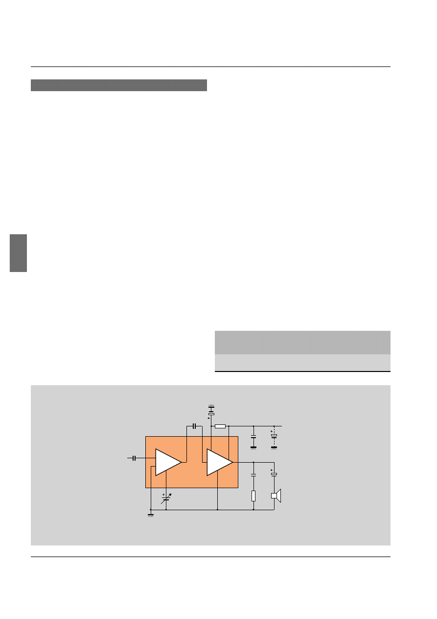
5-2
Audio Amplifier ICs
5
AUDIO AMPLIFIER IC
S
MAINS-POWERED SYSTEMS INCLUDING HI-FI & TV SOUND
TDA1013B
4 W to 10 W amplifier with DC volume
control
■
Separate preamplifier and power amplifier
■
Incorporates DC volume control with a control
range >80 dB (control voltage between 2 V and
7 V)
■
Well defined open-loop gain and fixed closed-loop
gain (power stage) of 38 dB (18 V supply, 8
Ω
load)
■
Minimum number of external components
■
Simple and low cost heatsinking
■
No switch-on/switch-off clicks
■
Output noise diminishes with reducing volume
This amplifier has a built-in DC volume control with a logarith-
mic characteristic providing control over a range of more than
80 dB. Its wide supply voltage range (10 V to 40 V) makes it
ideal for mains-powered equipment such as TV sets.
It comes in a 9-pin plastic SIL medium-power package offering
simple and low-cost heatsinking.
POWER OUTPUT AT d
tot
= 10%
power
supply
load
output
voltage
impedance
(W)
(V)
(
Ω
)
4.2
18
8
10
35
16
CONTR.
UNIT
AUDIO
AMP.
220 nF
DC
volume
control
9
7
1
4
3
2
220 k
Ω
0.1
µ
F
5
6
0.1
µ
F
470
µ
F
V P
0.1
µ
F
470
µ
F
3.3
Ω
8
input
MSA613
TDA1013B
1
µ
F
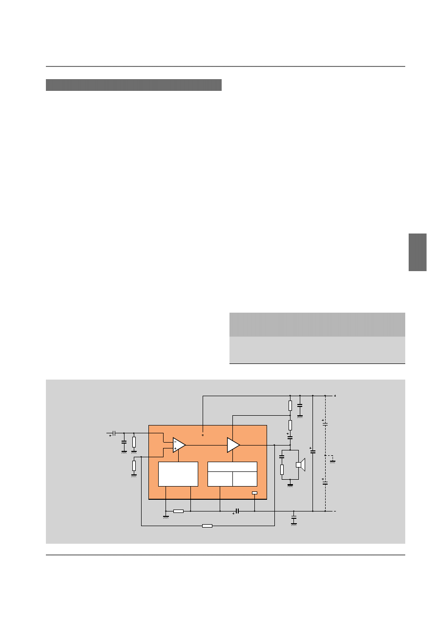
5-3
Audio Amplifier ICs
5
AUDIO AMPLIFIER IC
S
TDA1514A
50 W high-performance hi-fi amplifier
■
High ripple rejection of 72 dB
■
Standby feature with an activation level of <1 V at
pin 3. The supply voltage to obtain the standby
state is ±4.5 V to ±7 V. The standby supply current
is 20 mA.
■
Mute facility with an activation level of 2 V to 4.5 V
at pin 3
■
Thermal protection
■
Good supply voltage ripple rejection
■
Signal to noise ratio is 82 dB at P
o
= 50 mW,
R
s
= 2 k
Ω
■
High slew rate (10 V/µs)
■
Output protected against AC short-circuit
(asymmetrical power supply) and DC short-circuit
(symmetrical power supply) via SOAR protection
■
Externally adjustable closed-loop voltage gain of
20 dB to 46 dB
■
Low output offset voltage (2 mV) also allows 2
×
TDA1514A to be used in BTL configuration to
obtain output powers up to 100 W (see next page)
POWER OUTPUT WITH V
p
= ±27.5 V, R
L
= 8
Ω
power
d
tot
d
tot
output*
(W)
(%)
(dB)
32 (40)
0.003
-90
40 (50)
0.1
-60
51 (65)
10
-20
* values between brackets are for V
p
= ±24 V, R
L
= 4
Ω
With its high power output and high performance, this amplifi-
er is ideal for top quality mains-powered hi-fi systems, radios,
TV sets and digital audio systems.
The output transistors have total thermal and SOAR protection,
and the circuit embodies a special mute facility that operates for
a short period after switch-on to eliminate switch-on/switch-off
clicks. This period is preset by external components.
The IC can operate from either asymmetrical or symmetrical
power supplies (±7.5 V to ±30 V) and comes in a 9-pin plastic
SIL power package.
MSB408
VP
22 nF
3.3
Ω
VP
PROTECTION
SOAR
THERMAL
MUTE/STANDBY
6
7
470
Ω
1
9
20
k
Ω
680
Ω
220
pF
input
1
µ
F
3.3
µ
F
20 k
Ω
220
µ
F
150
Ω
82
Ω
470
nF
47
µ
F
2.2 mF
2.2 mF
3
8
2
4
5
TDA1514A
470 nF
MAINS-POWERED SYSTEMS INCLUDING HI-FI & TV SOUND
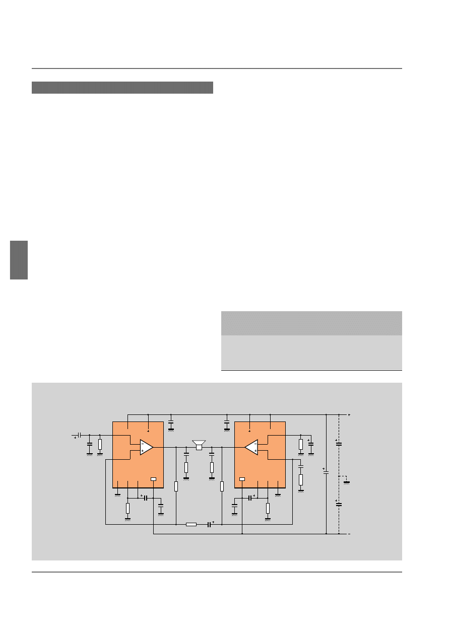
5-4
Audio Amplifier ICs
5
AUDIO AMPLIFIER IC
S
2
×
TDA1514A
100 W BTL high-performance hi-fi amplifier
The low output offset voltage (2 mV) of the TDA1514A (see
previous page) allows two of these ICs to be connected in BTL
configuration to obtain output powers of up to 100 W.
POWER OUTPUT AT d
tot
= –60 dB (0.1%)
power
supply
load
output
voltage
impedance
(W)
(V)
(
Ω
)
100
±24
8
70
±27.5
16
65
±20
8
55
±15
4
MSB409
VP
22 nF
3.3
Ω
VP
47
µ
F
2.2 mF
2.2 mF
1
9
20
k
Ω
220
pF
input
1
µ
F
TDA1514A
470 k
Ω
1
µ
F
8
3
2
4
470
nF
6
7
5
470 nF
20 k
Ω
22 nF
3.3
Ω
20 k
Ω
22
µ
F
1.3 k
Ω
1
9
TDA1514A
8
3
2
4
6
7
5
2.2 nF
100
Ω
470 nF
20
k
Ω
1
µ
F
470 k
Ω
1
µ
F
470
nF
MAINS-POWERED SYSTEMS INCLUDING HI-FI & TV SOUND
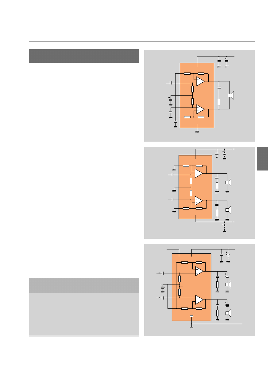
5-5
Audio Amplifier ICs
5
AUDIO AMPLIFIER IC
S
TDA1521(Q)/TDA2616(Q) AND
TDA1521A/TDA2615
2
×
6 W and 2
×
12 W hi-fi amplifiers
■
Very few external components required
■
Input muted during power-on and off (no switch-
on or switch-off clicks). This facility allows opera-
tion via remote control
■
Fixed voltage gain of 30 dB (±16 V supply 8
Ω
load)
for excellent gain balance between channels (with-
in 0.2 dB)
■
High supply voltage ripple rejection (50 dB at
100 Hz)
■
Channel separation 70 dB (symmetrical supply)
■
Meets IEC 268 and DIN 45500 hi-fi specifications
■
Output protected against short-circuit
■
Thermal protection
The TDA1521(Q) and TDA1521A, and the TDA2615 and
TDA2616(Q) are pin-compatible amplifiers for mains-powered
applications such as stereo TV sound channels and stereo radio.
They can operate from a symmetrical power supply of ±7.5 to
±21 V or from an asymmetrical power supply of 15 V to 42 V.
The low offset voltage (40 mV) between output and ground also
makes these amplifiers suitable for BTL applications.
The TDA1521A/TDA1521(Q) are identical to the TDA2615/
TDA2616(Q) except for a mute facility at pin 2 and internal
feedback interconnected for both channels to pin 8 on the
TDA2615/TDA2616(Q). This implies that the TDA2615 and
TDA2616(Q) have a fixed gain (30 dB).
The TDA1521A/TDA2615 come in 9-pin plastic SIL medium-
power packages. The TDA1521(Q)/TDA2616(Q) come in
9-pin plastic SIL power packages. The pins are bent to DIL for-
mat for the versions with a Q suffix.
POWER OUTPUT AT d
tot
= 0.5%
power
supply
load
output
voltage
impedance
(W)
(V)
(
Ω
)
TDA1521(Q)/TDA2616(Q): mono BTL
20 *
24
8
TDA1521(Q)/TDA2616(Q): stereo
2
×
12 **
±16
8
2
×
6
±12
8
2
×
10
±12
4
TDA1521A/TDA2615: stereo
2
×
6
±12
8
*
26 W at d
tot
= 10%
** 2
×
15 W at d
tot
= 10%
MSB406
2
3
7
100 nF
680
µ
F
VP
20 k
Ω
9
8
20 k
Ω
680
Ω
20 k
Ω
6
TDA1521(A)
1
680
Ω
20 k
Ω
4
22 nF
8.2
Ω
5
2.2 nF
220 nF
100
µ
F
input
220 nF
MSB407
2
3
7
100 nF
680
µ
F
VP
20 k
Ω
9
8
20 k
Ω
680
Ω
20 k
Ω
9
TDA1521(A)
1
680
Ω
20 k
Ω
4
22 nF
8.2
Ω
5
input 1
220 nF
input 2
220 nF
to
pin 5
22 nF
8.2
Ω
680
µ
F
VP
MLA940 - 1
100
nF
220
µ
F
P
V
4
TDA2615
TDA2616
3
7
1
5
680
Ω
20 k
Ω
R = 8
Ω
L
22
nF
680
µ
F
20 k
Ω
20 k
Ω
internal
1/2 V
P
9
8
680
Ω
20 k
Ω
8.2
Ω
22
nF
680
µ
F
8.2
Ω
220 nF
µ
F
V I
220 nF
V I
2
6
mute input
R = 8
Ω
L
100
TDA1521(A) in BTL mono configuration
TDA1521(A) in single-ended stereo configuration
TDA2615/TDA2616 in single-ended stereo configuration
MAINS-POWERED SYSTEMS INCLUDING HI-FI & TV SOUND
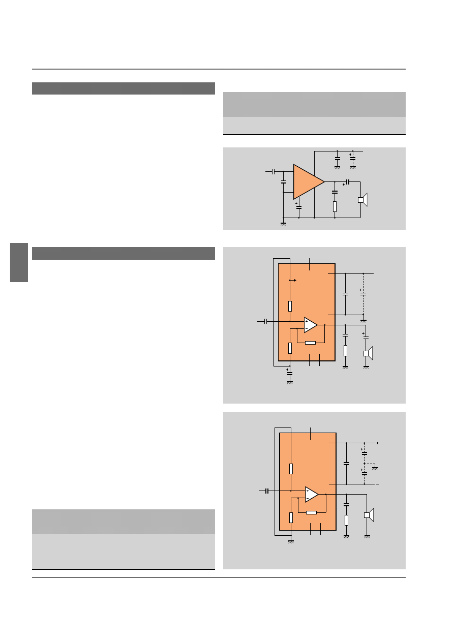
5-6
Audio Amplifier ICs
5
AUDIO AMPLIFIER IC
S
TDA2611A
4 W to 10 W amplifier
■
Few external components
■
Thermal protection
■
Well defined open-loop gain with simple quiescent
current setting and fixed closed-loop voltage gain
of 38 dB (18 V supply, 8
Ω
load)
This amplifier is ideal for the sound output stage of TV sets. It
can operate from supply voltages between 6 V and 35 V and
comes in a 9-pin plastic SIL medium-power package.
POWER OUTPUT AT d
tot
= 10%
power
supply
load
output
voltage
impedance
(W)
(V)
(
Ω
)
4.5
18
8
10
35
16
MSB415
input 1
330 nF
100 nF
3.3
Ω
330
µ
F
1
100 nF
VP
TDA2611A
220 pF
2
7
6
8
4
22
µ
F
TDA2613/TDA2614
6 W hi-fi amplifiers
■
Very few external components required
■
Input muted during power-on and off (no switch-
on or switch-off clicks)
■
Low offset voltage between output and ground
■
Meets IEC 268 and DIN 45500 hi-fi specifications
■
Output protected against short-circuit
■
Thermal protection
■
Fixed closed-loop voltage gain of 30 dB (24 V
supply, 8
Ω
load)
These are mono versions of the TDA1521A/TDA2615 and are
pin compatible with one channel of those ICs. They deliver 6 W
for mains-powered equipment such as TV sets and radios. They
can operate from an asymmetrical power supply of between 15
and 42 V or from a symmetrical power supply of between
±7.5 V and ±21 V.
The TDA2613 and TDA2614 are identical except for the mute
facility at pin 2 on the TDA2614.
They come in a 9-pin plastic SIL medium-power package.
POWER OUTPUT AT d
tot
= 0.5%
power
supply
load
output
voltage
impedance
(W)
(V)
(
Ω
)
6
24
8
6
±12
8
10
24
4
10
±12
4
MSB414
VP
input
220 nF
9
20 k
Ω
TDA2613
TDA2614
8.2
Ω
680
µ
F
8
680
Ω
20
k
Ω
6
5
100
nF
7
22
nF
2
3
n.c.
(1)
1
4
n.c. n.c.
680
µ
F
100
µ
F
to internal 1/2 VP
MSB413
VP
input
220 nF
9
20 k
Ω
TDA2613
TDA2614
8.2
Ω
680
µ
F
8
680
Ω
20 k
Ω
6
5
100
nF
7
680
µ
F
VP
22 nF
2
3
n.c.
(1)
1
4
n.c. n.c.
TDA2613/TDA2614 with asymmetrical power supply
(pin 2 connected for external mute on the TDA2614)
TDA2613/TDA2614 with symmetrical power supply
MAINS-POWERED SYSTEMS INCLUDING HI-FI & TV SOUND

A-1
Audio Amplifier ICs
A
APPENDICES
APPENDICES

A-2
Audio Amplifier ICs
A
Data
Data on our semiconductors for radio/audio systems are avail-
able in loose data sheets or are given in Philips Semiconductors
data handbook IC01a (ordering code 9398 183 00011) and
IC01b (ordering code 9398 183 10011).
Data for our semiconductors for TV and video systems are avail-
able in loose data sheets or a given in Philips Semiconductors
data handbooks IC02a (ordering code 9398 652 23011), IC02b
(ordering code 9398 652 24011) and IC02c (ordering code
9398 652 24011).
Application Notes and Leaflets
The following Philips Semiconductors Application Notes relat-
ing to audio amplifiers are available:
1. “TDA1013B Audio amplifier with DC volume control”
Philips Semiconductors Application Note NBA/AN9005.
2. “Recorder IC TDA1016 for portable applications” Philips
Semiconductors Application Note NBA8301.
3. “TDA1514A Hi-fi power amplifiers” Philips Semiconductors
Application Note NBA/AN8911.
4. “Audio power ICs for car radios” Philips Semiconductors
Application Note NBA9001 (ordering code: 9398 078
30011).
5. “TDA1551Q, TDA1554Q, TDA1555Q and TDA1558Q
audio power amplifiers for car radio” Philips Semiconductors
Application Note NBA/AN9202.
6. “TDA1552Q/53(A)Q, TDA1556Q and TDA1557Q double
BTL amplifiers” Philips Semiconductors Application Note
NBA/AN9013.
7. “TDA1556Q 2
×
22 W BTL amplifier with differential
inputs” Philips Semiconductors Leaflet.
8. “Economic 6 W hi-fi audio amplifier for mains-fed applica-
tions” Philips Semiconductors Application Note NBA/
AN8902.
9. “TDA2614: economic 6.5 W hi-fi audio amplifier for mains-
fed applications” Philips Semiconductors Application Note
NBA/AN9109.
APPENDICES
FURTHER INFORMATION
10. “6.5 W stereo hi-fi audio amplifier for mains-fed applica-
tions” Philips Semiconductors Application Note
NBA/AN9110.
11. “12 W stereo hi-fi audio amplifier (20 W BTL)” Philips
Semiconductors Application Note NBA/AN9205.
12. “TDA7052A; 1 W BTL mono audio amplifier with DC vol-
ume control” Philips Semiconductors Application Note
NBA/AN9207.
13. “TDA7052/7053: 1 W componentless BTL mono/stereo
audio amplifiers” Philips Semiconductors Application Note
NBA8907 (ordering code: 9398 068 10011).
14. “TDA7056A; 3 W BTL mono audio amplifier with DC
volume control” Philips Semiconductors Application Note
NBA/AN9208.
15. “3 W mono BTL audio amplifier” Philips Semiconductors
Application Note NBA/AN9009.
16. “TDA7057 3 W componentless BTL stereo audio amplifier”
Philips Semiconductors Application Note NBA/AN9009.
17. “TDA1560Q power lifting amplifier (class-H)” Philips
Semiconductors Application Note NBA/AN9206.
For data sheets/handbooks and Application Notes, please con-
tact your local Philips Semiconductors sales organization at the
address listed on the back cover.
APPENDIX 1

A-3
Audio Amplifier ICs
A
INDEX OF AUDIO AMPLIFIER IC
S
APPENDICES
Type number
Description
Application*
Page
Preamplifier plus 3.4 to 12 W power amplifier
4 W to 10 W amplifier with DC volume control
2 W power and record/playback preamplifier
60 mW headphone/line output driver
50 W high-performance hi-fi amplifier
22 W BTL amplifier with differential inputs
23 W high-efficiency power amplifier
1 W/0.5 W BTL amplifier with DC volume control
1 W/0.5 W BTL amplifier with DC volume control
5 W BTL amplifier with DC volume control
5 W BTL amplifier with DC volume control
1 W BTL amplifiers with standby selection
1 W BTL amplifiers with digital volume control
Low-voltage BTL mono amplifiers
Low-voltage BTL stereo amplifiers
40 W BTL amplifier with diagnostics
7 W amplifier with diagnostics
12 W amplifier with diagnostics
25 W BTL power amplifier with differential inputs
Dual common-mode rejection differential line drivers
Dual common-mode rejection differential line driver
Dual common-mode rejection differential line driver
Dual common-mode rejection differential line driver
Dual common-mode rejection differential line receiver
* c = car radios/power boosters, m = mains-powered equipment, p = portable radio/audio equipment
APPENDIX 2
Wyszukiwarka
Podobne podstrony:
BP4078 Class D Audio Power Amplifier
IRF 60W audio Power Amplifier Using Complementary HEXFETs
Power 400 Watts Hi Fi High End Audio Power Amplifier
Designing Audio Power Amplifiers
Guidelines For Measuring Audio Power Amplifier Performance (Texas Instruments)
Daniel H Cheever A New Methodology for Audio Frequency Power Amplifier Testing Based On Psychoacoust
McMartin LT2000D Power Amplifier
AGH Analog electronics Chapter III 5 Power amplifiers
Pioneer DEHP825 Power Amplifier Section
20 Watt Channel Stereo Power Amplifier
60 100W Hi Fi Power Amplifier
500W Subwoofer Power Amplifier (Updated)
Power Amplifiers With Valves An Approach And A Practical Circuit (Claus Byrith)
Directory of integrated power amplifiers TDA
JBL Power Amplifier GTS50A
60 Watt Into 8 Ohms Power Amplifier
McMartin LT2000D Power Amplifier
McMartin LT2000D Power Amplifier
Subwoofer Power Amplifier
więcej podobnych podstron