
Rev C, November 1999
November 2,1999
1
AN4003
PC POWER SUPPLY DESIGN WITH KA3511
Sang-Tae Im
1. GENERAL DESCRIPTION
The KA3511 is a fixed-frequency improved-performance pulse-width modulation control circuit with
complete housekeeping circuitry for use in the secondary side of SMPS (Switched mode power
supply). It contains various functions, which are precision voltage reference, over voltage protec-
tion, under voltage protection, remote on/off control, power good signal generator and etc.
OVP (Over voltage protection) section
It has OVP functions for +3.3V,+5V,+12V and PT outputs. The circuit is made up of a comparator
with four detecting inputs and without hysteresis voltage. Especially, PT (Pin16) is prepared for an
extra OVP input or another protection signal.
UVP (Under voltage protection) section
It also has UVP functions for +3.3V, +5V, +12V outputs. The block is made up of a comparator with
three detecting inputs and without hysteresis voltage.
Remote on/off section
Remote on/off section is used to control SMPS externally. If a high signal is supplied to the remote
on/off input, PWM signal becomes a high state and all secondary outputs are grounded. The
remote on/off signal is transferred with some on-delay and off-delay time of 8ms, 24ms respec-
tively.
Precision reference section
The reference voltage trimmed to
±
2% (4.9V<Vref<5.1V)
PG (Power good signal generator) section
Power good signal generator is to monitor the voltage level of power supply for safe operation of a
microprocessor.
KA3511 requires few external components to accomplish a complete housekeeping circuits for
SMPS. The KA3511 is available in a 22-pin dual in-line package.
2
Rev C, November 1999
ORDERING INFORMATION
FEATURES
• Complete PWM control and house keeping circuitry
• Few external components
• Precision voltage reference trimmed to 2%
• Dual output for push-pull operation
• Each output TR for 200mA sink current
• Variable duty cycle by dead time control
• Soft start capability by using dead time control
• Double pulse suppression logic
• Over voltage protection for 3.3V / 5V / 12V
• Under voltage protection for 3.3V / 5V / 12V
• One more external input for various protection (PT)
• Remote on/off control function (PS-ON)
• Latch function controlled by remote and protection input
• Power good signal generator with hysteresis
• 22-Pin dual in-line package
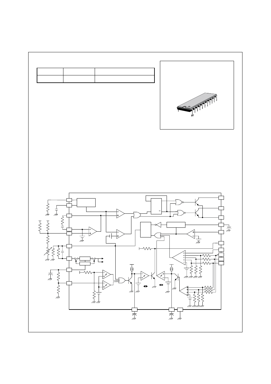
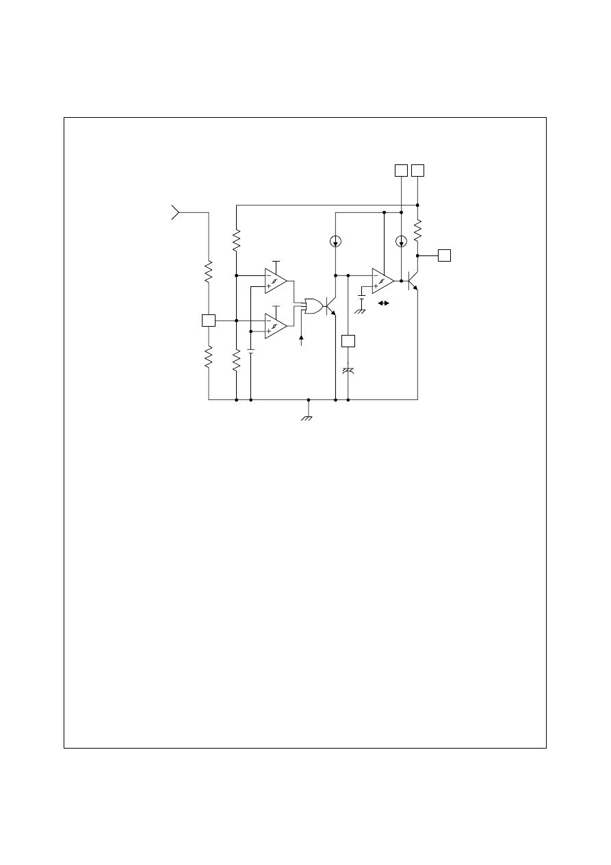
2. BLOCK DIAGRAM
Device Package Operating
Temperature
KA3511 22
DIP
-25
°
C ~ 85
°
C
7
8
OSCILLATOR
2
3
4
19
12
VREF
Start Up
1
9
DELAY
CONTROLLER
17
18
10
20
22
21
5
6
T
REM
11
16
13
14
15
PT
V12
V5
V3.3
PG
REM
(PS-ON)
E
C2
C1
REMOTE ON/OFF
1.4V
1.25V
VREF
5V
OVP
COMP
1.25V
UVP
COMP
GND
T
UVP
2.2uF
T
PG
2.2uF
COMP3
1.8V
0.6V
1.8V
0.6V
PG
GENERATOR
VREF
Ichag
COMP2
COMP1
1.25V
0.1V
DEAD TIME
CONTROLLER
PWM
CONTROL
Q
R
S
CK
D
Q
Q
1.25V
INTERNAL
BIAS
5V
DET
V
CC
VREF
DEAD TIME
CONTROL
E/A(+)
E/A(-)
V5
V12
COMP
C
T
R
T
22-DIP-400
3
Rev C, November 1999
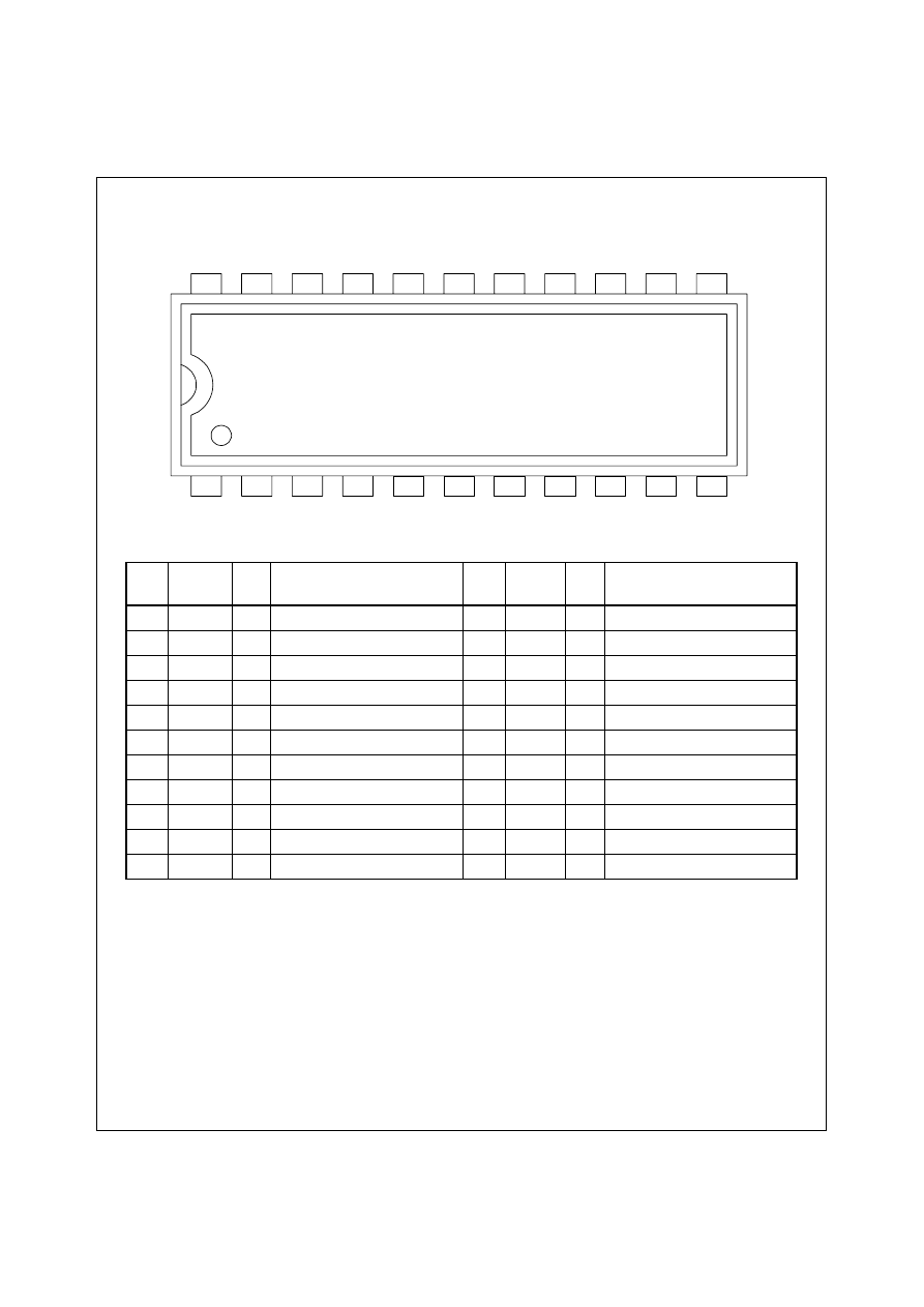
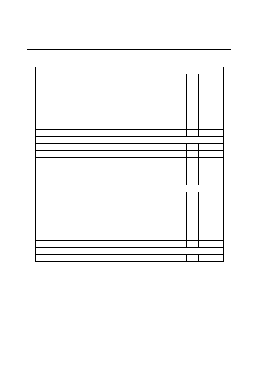
3. PIN DESCRIPTION
Pin
No.
Name
I/O Function
Pin
No.
Name
I/O
Function
1 V
CC
I
Supply voltage
12
Vref
O
Precision reference VTG
2
COMP
O
E/A output
13
V3.3
I
OVP, UVP input for 3.3V
3
E/A(-)
I
E/A (-) input
14
V5
I
OVP, UVP input for 5V
4
E/A(+)
I
E/A (+) input
15
V12
I
OVP, UVP input for 12V
5
TREM
–
Remote on/off delay
16
PT
I
Extra protection input
6
REM
I
Remote on/off input
17
T
UVP
– UVP
delay
7
RT
–
Oscillation freq. setting R
18
GND
–
Signal ground
8
CT
–
Oscillation freq. setting C
19
DTC
I
Deadtime control input
9 DET I Detect
input
20 C2 O
Output
2
10 T
PG
–
PG delay
21
E
–
Power ground
11
PG
O
Power good signal output
22
C1
O
Output 1
KA3511
V
CC
COMPE/A(-)
EA(+)
TREM
REM
RT
CT
DET
TP
G
P
G
#1
#11
Vref
#12
V3.3
#22
V5
V12
PT
TUVP
GND
DTC
C2
E
C1

4
Rev C, November 1999
Pin
No.
Name Function
1 V
CC
Supply voltage. Operating range is 14V~30V. V
CC
=20V, Ta=25
°
C at test.
2
COMP Error amplifier output. It is connected to non-inverting input of pulse width
modulator comparator.
3
E/A(-)
Error amplifier inverting input. Its reference voltage is always 1.25V.
4
E/A(+)
Error amplifier non-inverting input feedback voltage.This pin may be used to
sense power supply output voltage.
5
TREM
Remote on/off delay. Ton/Toff=8ms/24ms (Typ.) with C=0.1µF. Its high/low
threshold voltage is 1.8V/0.6V.
6
REM
Remote on/off input. It is TTL operation and its threshold voltage is 1.4V. Voltage
at this pin can reach normal 4.6V, with absolutely maximum voltage, 5.25V. If
REM = “Low”, PWM = “Low”. That means the main SMPS is operational. When
REM = “High”, then PWM = “High” and the main SMPS is turned-off.
7
RT
Oscillation frequency setting R. (Test Condition R
T
=10k
Ω
)
8
CT
Oscillation frequency setting C. (Test Condition C
T
=0.01µF)
9
DET
Under-voltage detect pin. Its threshold voltage is 1.25V Typ.
10 T
PG
PG delay. Td=250ms (Typ) with C
PG
=2.2µF. The high/low threshold voltage are
1.8V/0.6V and the voltage of Pin10 is clamped at 2.9V for noise margin.
11
PG
Power good output signal. PG = “High” means that the power is “Good” for
operation and PG = “Low” means “Power fail”.
12
Vref
Precision voltage reference trimmed to 2%. (Typical Value = 5.03V)
13
V3.3
Over voltage protection for output 3.3V. (Typical Value = 4.1V)
14
V5
Over voltage protection for output 5V. (Typical Value = 6.2V)
15
V12
Over voltage protection for output 12V. (Typical Value = 14.2V)
16
PT
This is prepared for an extra OVP input or another protection signal. (Typical
Value = 1.25V)
17 T
UVP
Timing pin for under voltage protection blank-out time. Its threshold voltage is
1.8V and clamped at 2.9V after full charging. Target of delay time is 250ms and
it is realized through external (C=2.2µF).
18 GND Signal
ground.
19
DTC
Deadtime control input. The dead-time control comparator has an effective
120mV input offset which limits the minimum output dead time. Dead time may
be imposed on the output by setting the dead time control input to a fixed
voltage, ranging between 0V to 3.3V.
20
C2
Output drive pin for push-pull operation.
21 E Power
ground.
22
C1
Output drive pin for push-pull operation.
5
Rev C, November 1999
4. ABSOLUTE MAXIMUM RATINGS
TEMPERATURE CHARACTERISTICS
Characteristic
Symbol Value Unit
Supply voltage
V
CC
40 V
Collector output voltage
V
C1
, V
C2
40 V
Collector output current
I
C1
, I
C2
200 mA
Power dissipation
P
D
1 W
Operating temperature
T
OPR
-25 to 85
°C
Storage temperature
T
STG
-65 to 150
°C
Characteristic
Symbol
Value
Unit
Min. Typ.
Max.
Temperature coefficient of Vref (-25 °C<Ta<85°C)
∆
Vref/
∆
T – 0.01 –
%/°C
6
Rev C, November 1999
5. ELECTRICAL CHARACTERISTICS (V
CC
=20V, T
A
=25°C)
Characteristic Symbol
Test
Condition
Value
Unit
Min. Typ. Max.
REFERENCE SECTION
Reference output voltage
Vref
Iref=1mA
4.9
5
5.1
V
Line regulation
∆
Vref.
LINE
14V<V
CC
<30V –
2.0
25
mV
Load regulation
∆
Vref.
LOAD
1mA<Iref<10mA –
1.0
15
mV
Temperature coefficient of Vref
(1)
∆
Vref/
∆
T -25°C<Ta<85°C –
0.01
–
%/°C
Short-circuit output current
I
SC
Vref=0
15
35
75
mA
OSCILLATOR SECTION
Oscillation frequency
fosc
C
T
=0.01µF, R
T
=12k – 10 –
kHz
Frequency change with
temperature
(1)
fosc/T C
T
=0.01µF, R
T
=12k – 2 – %
DEAD TIME CONTROL SECTION
Input bias current
I
B(DT)
– -2.0
-10
µA
Maximum duty voltage
DC
MAX
Pin19
(DTC)=0V
45
48
50
%
Input threshold voltage
V
TH(DT)
Zero Duty Cycle
–
3.0
3.3
V
Max. Duty Cycle
0
–
–
ERROR AMP SECTION
Inverting reference voltage
Vref(EA)
1.20
1.25
1.30
%
Input bias current
I
B(EA)
V
COMP
=2.5V
–
-0.1
-1.0
µA
Open-loop voltage gain
(1)
G
VO
0.5V<V
COMP
<3.5V 70
95
–
dB
Unit-gain bandwidth
(1)
BW
– 650 –
kHz
Output sink current
I
SINK
V
COMP
=0.7V 0.3
0.9
–
mA
Output source current
I
SOURCE
V
COMP
=3.5V
-2.0
-4.0
–
mA
PWM COMPARATOR SECTION
Input threshold voltage
V
TH(PWM)
Zero Duty Cycle
–
4
4.5
V
OUTPUT SECTION
Output saturation voltage
V
CE(SAT)
I
C
=200mA –
1.1
1.3
V
Collector off-state current
I
C(off)
V
CC
=V
C
=30V, V
E
=0V
–
2
100 µA
Rising time
T
R
–
100
200
ns
Falling time
T
F
–
50
200
ns
PROTECTION SECTION
Over voltage protection for 3.3V
V
OVP1
3.8
4.1
4.3
V
7
Rev C, November 1999
5. ELECTRICAL CHARACTERISTICS (continued)
Notes:
1. These Parameters, although guaranteed over their recommended operating conditions are not 100%
tested in production.
2. REM on delay time (Pin6 REM: “L”
→
“H”),
REM off delay time (Pin6 REM: “H”
→
“L”)
Characteristic
Symbol Test
Condition
Value
Unit
Min. Typ. Max.
Over voltage protection for 5V
V
OVP2
–
5.8 6.2 6.6 V
Over voltage protection for 12V
V
OVP3
–
13.5 14.2 15.0 V
Input threshold voltage for PT
V
PT
–
1.20 1.25 1.30
Under voltage protection for 3.3V
V
UVP1
–
2.1
2.3
2.5
V
Under voltage protection for 5V
V
UVP2
–
3.7 4.0 4.3 V
Under voltage protection for 12V
V
UVP3
–
9.2 10 10.8 V
Charging current for UVP delay
I
CHG.UVP
C=2.2µF,
V
TH
=1.8V
-10
-15
-23
uA
UVP Delay Time
T
D.UVP
C=2.2µF 100
260
500
ms
REMOTE ON/OFF SECTION
REM on input voltage
V
REMH
I
REM
= -200µA
2.0
–
–
V
REM off input voltage
V
REML
–
– – 0.8
V
REM off input bias voltage
I
REML
V
REM
=0.4V
–
–
-1.6
mA
REM on open voltage
V
REM(OPEN)
–
2.0 – 5.25 V
REM on delay time
Ton
C=0.1µF
4
8
14
ms
REM off delay time
Toff
C=0.1µF
16
24
34
ms
REMOTE ON/OFF SECTION
(2)
Detecting input voltage
V
IN(DET)
–
1.20 1.25 1.30 V
Detecting V5 voltage
V
5(DET)
–
4.1 4.3 4.5 V
Hysteresis voltage 1
HY1
COMP1, 2
10
40
80
mV
Hysteresis voltage 2
HY2
COMP3
0.6
1.2
–
V
PG output load resistor
R
PG
–
0.5 1 2 k
Ω
Charging current for PG delay
I
CHG.PG
C=2.2µF, V
TH
=1.8V
-10
-15
-23
uA
PG delay time
T
D.PG
C=2.2µF 100
260
500
ms
PG output saturation voltage
V
SAT(PG)
I
PG
=10mA
–
0.4
0.2
V
TOTAL DEVICE
Standby supply current
I
CC
–
–
10
20
mA
8
Rev C, November 1999
6. BLOCK DESCRIPTION & APPLICATION INFORMATIONS
6.1 OSCILLATOR BLOCK
Figure 1. Oscillator R
T
, C
T
The KA3511 is a fixed-frequency pulse width modulation control circuit. An internal-linear sawtooth
oscillator is frequency-programmable by two external components, R
T
and C
T
. The oscillator fre-
quency is determined by
Figure 2. Oscillator Frequency vs. Timing Resistance
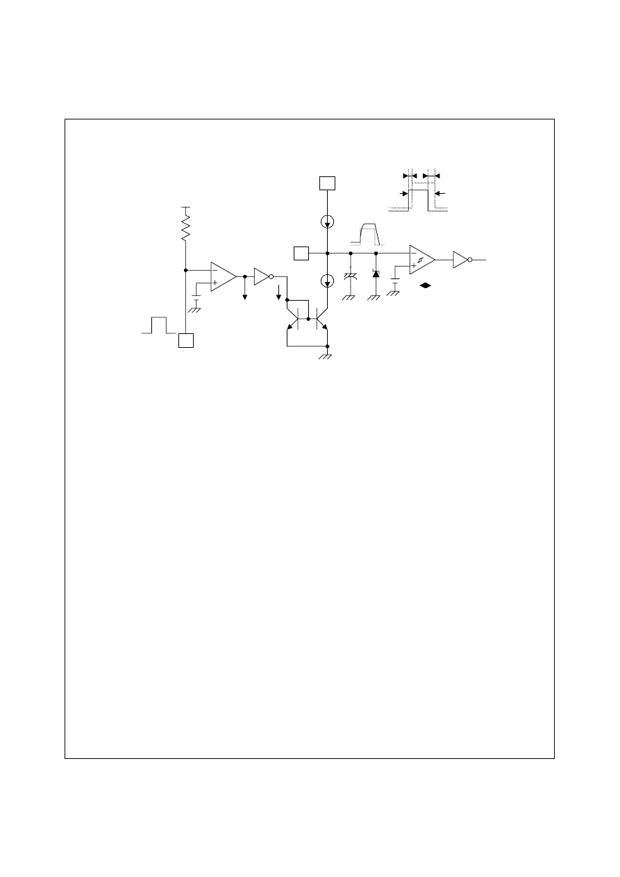
6.2 PWM CONTROL BLOCK
Output pulse width modulation is accomplished by comparison of the positive sawtooth waveform
across capacitor C
T
to either of two control signals. The NOR gates, which drive output transistors
Q1 and Q2, are enabled only when the flip-flop clock-input line is in its low state. This happens only
during that portion of time when the sawtooth voltage is greater than the control signals. Therefore,
an increase in control-signal amplitude causes a corresponding linear decrease of output pulse
width. (Refer to the timing diagram shown in Figure 4)
Vref
V
CC
C
T
R
T
12
1
12
12
fosc
1.1
R
T
C
T
×
---------------------
=
300K
2K
5K
10K
20K
50K 100K
200K
500K 1M
100K
10K
1K
100
30
1K
I
O
-
O
S
C
IL
L
A
TO
R
FR
E
Q
U
E
N
C
Y
R
T
. TIMING RESISTANCE(
Ω
)
VCC=15V
1.0
µ
F
0.1
µ
F
CT=0.01
µ
F
0.001
µ
F
9
Rev C, November 1999
Figure 3. PWM Control Block
The control signals are external inputs that can be fed into the dead-time control, the error amplifier
inputs, or the feedback input. The dead-time control comparator has an effective 120mV input off-
set which limits the minimum output dead time. Dead time may be imposed on the output by set-
ting the dead time control input to a fixed voltage, ranging between 0V to 3.3V.
The pulse width modulator comparator provides a means for the error amplifier to adjust the output
pulse width from the maximum percent on-time, established by the dead time control input, down
to zero, as the voltage at the feedback pin varies from 0.5V to 3.5V. The error amplifier may be
used to sense power-supply output voltage, and its output is connect to noninverting input of the
pulse width modulator comparator. With this configuration, the amplifier that demands minimum
output on time, dominates control of the loop.
When capacitor C
T
is discharged, a positive pulse is generated on the output of the dead time
comparator, which clocks the pulse-steering flip-flop and inhibits the output transistors, Q1 and Q2.
The pulse-steering flip-flop directs the modulated pulses to each of the two output transistors
always for push-pull operation. The output frequency is equal to half that of the oscillator.
The KA3511 has an internal 5.0V reference capable of sourcing up to 10mA of load current for
external bias circuits. The reference has an internal accuracy of ±2% with typical thermal drift of
less than 50mV over an operating temperature range of -25°C to 85°C
OSCILLATOR
R
T
C
T
7
8
2
4
3
CK
D
Q
Q
COMP
PWM
CONTROL
1.25V
Q1
Q2
Output
Drive
0.12V
DEAD TIME
CONTROLLER
10
Rev C, November 1999
Figure 4. Operating Waveform
6.3 DEADTIME CONTROL for SOFT-START
Figure 5. Soft-Start Circuit
Deadtime control for soft-start makes a power supply output rising time (Typ. 15ms) to reduce out-
put ringing voltage for 3.3V, 5V, and 12V. If output rising time is too fast, output ringing voltage
reaches OVP level.
You can make a soft start function by add external components R1, R2 and C1 (refer to figure 5).
At first the main power is turned-on, the deadtime control voltage keeps high state ( · = · 3V), and
then go to the low voltage( · = · 105mV) that devided by R1, R2.
Feedback
Dead-time
control
Ct
Ck
Q
Q
Output Q1
Output Q2
19
12
3mA
Vref
R1
47k
R2
1k
DTC
Remote
ON/OFF
+
C1
22uF
V
DTC LOW
R2
R1
R2
+
----------------------
Vref(5V) = 104.9mV
×
=
11
Rev C, November 1999
So Output Duty Ratio will change from the minimum duty ratio to the maximum duty ratio.
Also, if the remote voltage is high, the deadtime control voltage will keep 3V (=3mA xR2 (1k
Ω
)) by
the internal 3mA current source for soft start. Therefore, when the remote voltage is low, the dead-
time control voltage will be changed from 3V to almost ground potential. And its soft start time
dependent on external capacitor C1.
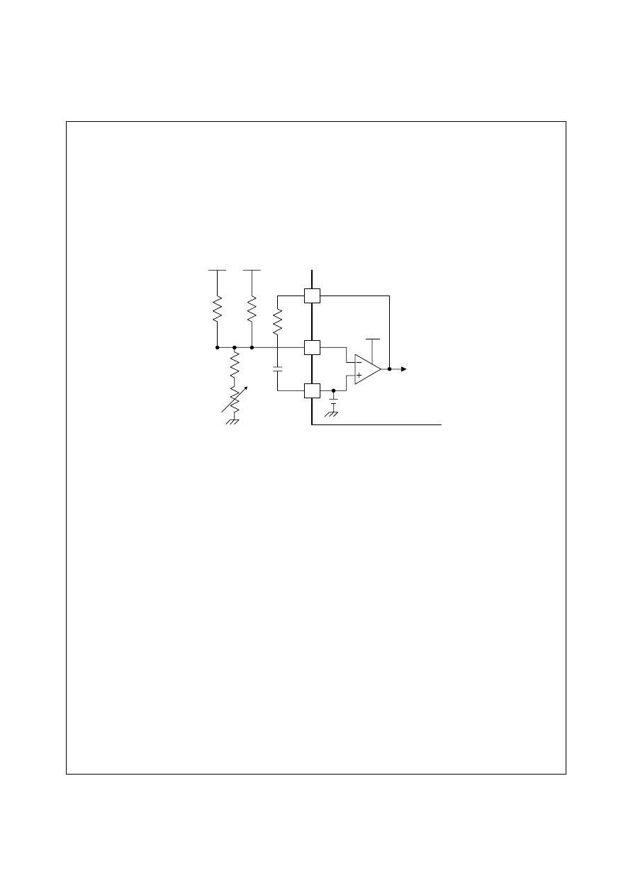
6.4 OUTPUT VOLTAGE REGULATION
Figure 6. Output Regulation Circuit
+5V/+12V output voltages are determined by resistor ratio of R1,R2,R3 and R4. The resistor value
can be changed by set condition and requirements.
R5, C1 are the compensation circuit for stability.
If output voltage (+5V or +12V) is increase, duty ratio of main power switch will be reduced by
PWM control comparator signal and error amplifier output. Therefore the output voltage will be
reduced.
On the contrary, if output voltage (+5V or +12V) is reduce, duty ratio of main power switch will be
increased by PWM control comparator signal and error amplifier output. Therefore the output volt-
age will be increased. So the output voltage of power supply will be regulated.
2
4
3
+5V
+12V
COMP
E/A(-)
E/A(+)
R5
1k
Ω
R2
33k
Ω
R1
11k
Ω
R3
2k
Ω
R4
1k
Ω
C1
103
Vref
PWM Control
Comparator
1.25V
Err-Amp
12
Rev C, November 1999
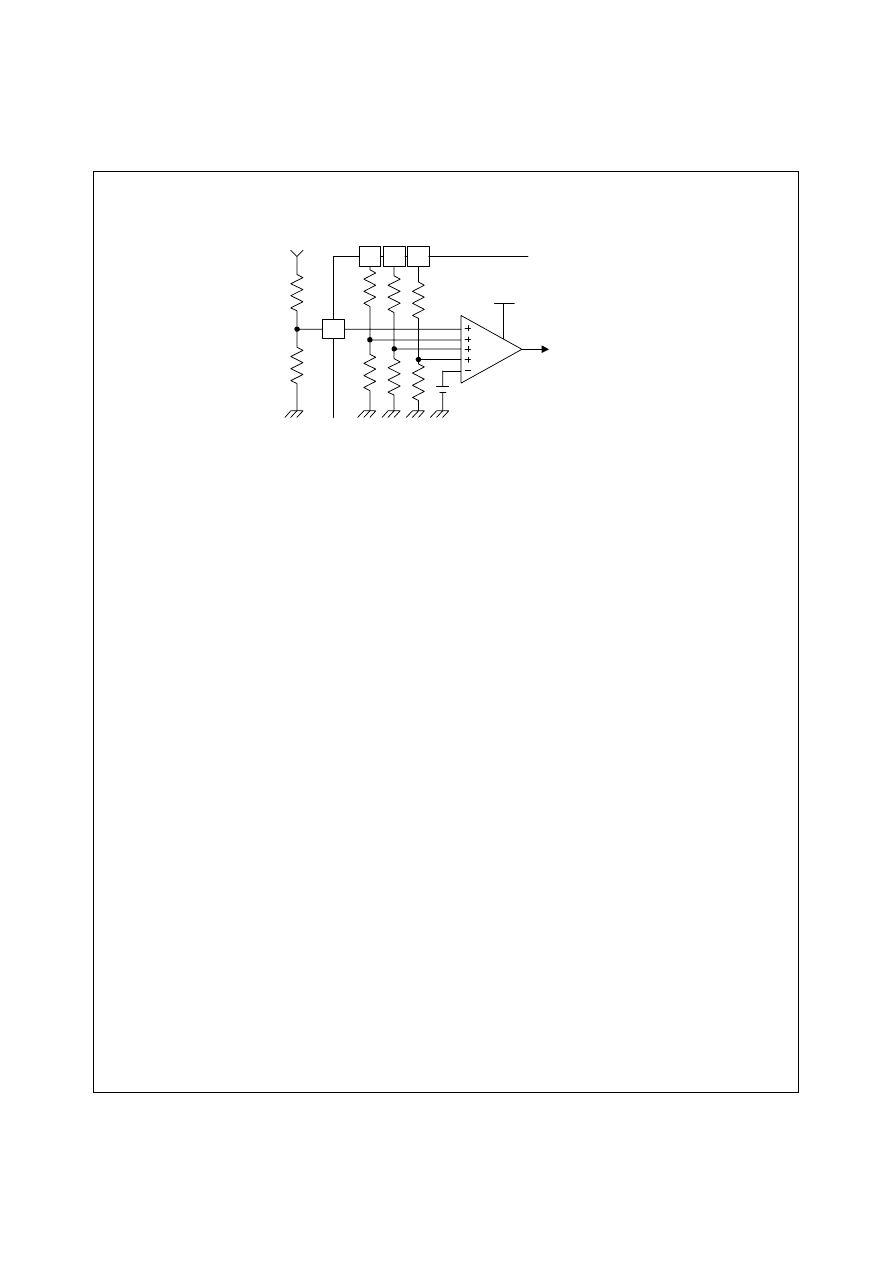
6.5 OVP BLOCK
OVP function is simply realized by connecting Pin13, Pin14, Pin15 to each secondary output. R1,
2, 3, 4, 5, 6 are internal resistors of the IC. Each OVP level is determined by resistor ratio and the
typical values are 4.1V/6.2V/14.2V.
OVP Detecting voltage for +3.3V
OVP Detecting voltage for +5V
OVP Detecting voltage for +12V
Especially, pin16 (PT) is prepared for extra OVP input or another protection signal. That is, if you
want over voltage protection of extra output voltage, then you can make a function with two exter-
nal resistors.
OVP Detecting voltage for PT
In the case of OVP, system designer should know a fact that the main power can be dropped after
a little time because of system delay, even if PWM is triggered by OVP.
So when the OVP level is tested with a set, you should check the secondary outputs (+3.3V/+5V/
+12V) and PG (Pin11) simultaneously. you can know the each OVP level as checking each output
voltage in just time that PG (Pin11) is triggered from high to low.
Vref=5V
13
14
15
16
R101
R102
PT
R1
R3
R5
3.3V 5V
12V
R2
R4
R6
1.25V
D
C
B
A
OVP COMP
SET of
R/S Latch
R102, R102
: External Components
VO
V
OVP 1
+3.3V
(
)
R
1
R
2
+
R
2
--------------------
V
A
×
R
1
R
2
+
R
2
--------------------
Vref
×
4.1V
=
=
=
V
OVP 2
+5V
(
)
R
3
R
4
+
R
4
--------------------
V
B
×
R
3
R
4
+
R
4
--------------------
Vref
×
6.2V
=
=
=
V
OVP 3
+12V
(
)
R
5
R
6
+
R
6
--------------------
V
C
×
R
5
R
6
+
R
6
--------------------
Vref
×
14.2V
=
=
=
V
PT
R
101
R
102
+
R
102
-------------------------------
V
D
×
R
101
R
102
+
R
102
-------------------------------
Vref
×
=
=

13
Rev C, November 1999
6.6 UVP BLOCK
The KA3511 has UVP functions for +3.3V, +5V, +12V Outputs. The block is made up of three input
comparators. Each UVP level is determined by resistor ratio and the typical values are 2.3V/4V/
10V.
UVP Detecting voltage for +3.3V
UVP Detecting voltage for +5V
UVP Detecting voltage for +12V
13
14
15
Vref=5V
SET of
R/S Latch
R1
R3
R5
R2
R2
R6
1.25V
A
B
C
UVP COMP
3.3V
5V
12V
V
UVP 1
+3.3V
(
)
R
1
R
2
+
R
2
--------------------
V
A
×
R
1
R
2
+
R
2
--------------------
Vref
×
2.3V
=
=
=
V
UVP 2
+5V
(
)
R
1
R
2
+
R
2
--------------------
V
A
×
R
1
R
2
+
R
2
--------------------
Vref
×
4V
=
=
=
V
UVP 3
+12V
(
)
R
1
R
2
+
R
2
--------------------
V
A
×
R
1
R
2
+
R
2
--------------------
Vref
×
10V
=
=
=
14
Rev C, November 1999
6.7 REMOTE ON/OFF & DELAY BLOCK
Figure 9. Remote ON/OFF Delay Block
Remote ON/OFF section is controlled by a microprocessor. If a high signal is supplied to the
remote ON/OFF input (Pin6), the output of COMP6 becomes high status. The output signal is
transferred to ON/OFF delay block and PG block.
If no signal is supplied to Pin6, Pin6 maintains high status (=5V) for Rpull.
When Remote ON/OFF is high, it produces PWM (Pin6) “High” signal after ON delay time (about
8ms) for stabilizing system.
Then, all outputs (+3.3V, +5V, +12V) are grounded.
When Remote ON/OFF is changed to “Low”, it produces PWM “Low” signal after OFF delay time
(about 24ms) for stabilizing the system.
If REM is low, then PWM is low. That means the main SMPS is operational. When REM is high,
PWM is high and the main SMPS is turned-off.
ON/OFF delay Time can be calculated by following equation.
(K1, K2: Constant value gotten by test)
In above equation, typical capacitor value is 0.1uF. If the capacitor is changed to larger value, it
can cause malfunction in case of AC power on at remote High. Because PWM maintains low sta-
tus and main power turns on for on delay time. So you should use 0.1uF or smaller capacitor.
6
5
12
Rpull
5V
COMP6
COMP
PG
Block
Remote On/Off
REM
Q1
Q2
Ion/Ioff
Ion
Trem
Trem
0.1uF
+
2.2V
0.6V
1.8V
B
C
Vref
PWM
REM
Ton
Toff
Ton
K
1
Ctrem
∆
Von
×
Ion
---------------------------------------
0.95
0.1
µ
F
2V
×
23
µ
A
------------------------------
×
≈
×
= 8.2msec
=
Toff
K
2
Ctrem
∆
Voff
×
Ioff
---------------------------------------
0.8
0.1
µ
F
2.1V
×
8
µ
A
-----------------------------------
×
≈
×
= 24msec
=
15
Rev C, November 1999
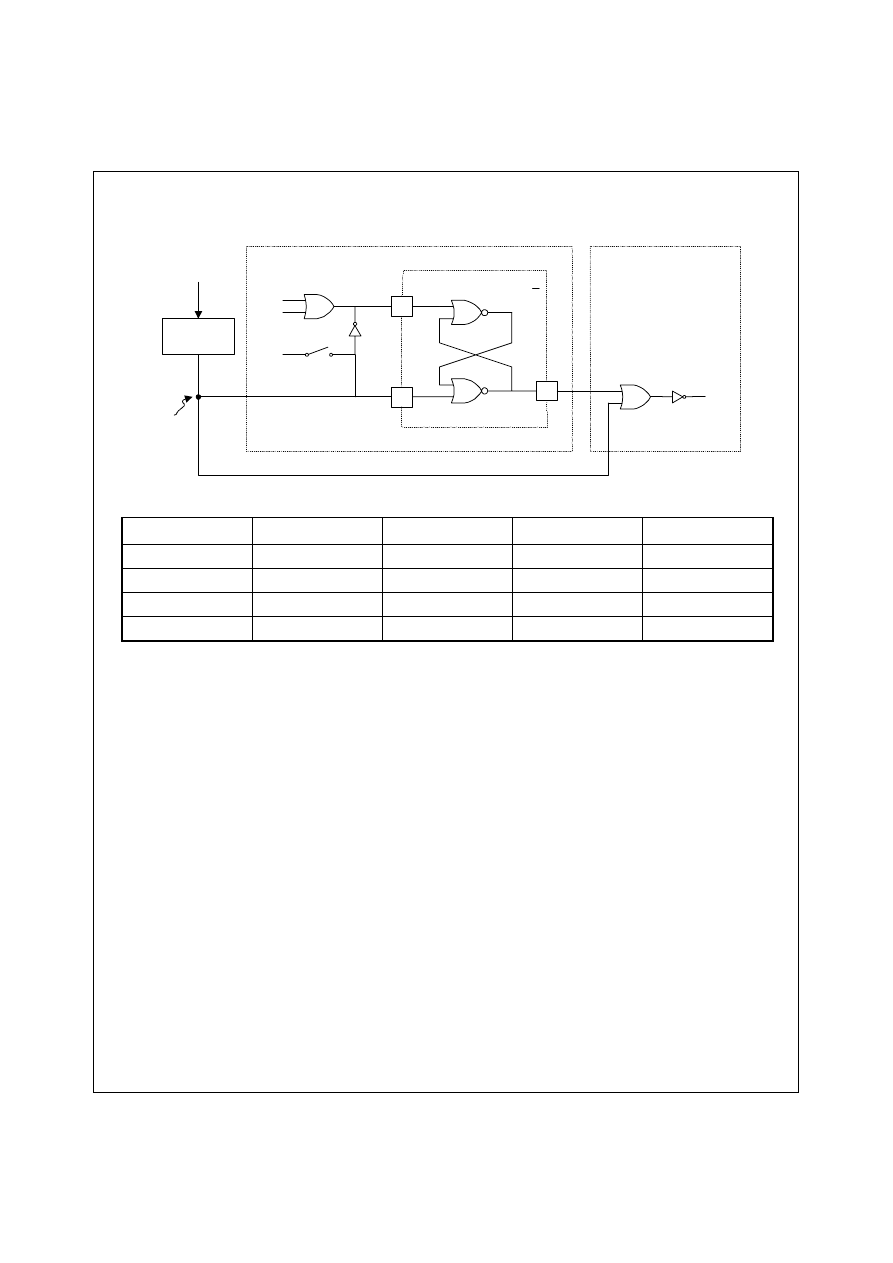
6.8 R/S FLIP FLOP (LATCH) BLOCK
Figure 10. R-S F/F Block Diagram
There is a R-S F/F (Latch) circuit for shutdown operation in the KA3511. R-S F/F (Latch) is con-
trolled by OVP, UVP, and some delayed remote ON/OFF signal.
If any output of OVP or UVP is High, SET signal of R-S F/F is high status and it produces PWM
“High” and main power is turned off. When remote signal is high, its delayed output signal is sup-
plied to RESET port of R-S F/F and it produces SET low. So output Q is low status. At this time,
PWM maintains high status by delayed remote high signal.
After main power is turned-off by OVP/UVP and initialized by remote, if remote signal is changed to
low, main power becomes operational.
When you test KA3511, Remote ON/OFF signal should be toggled once for initializing.
OVP+ SET RESET
Qn+1 Qn+1
Low Low Low Qn Qn
Low Low High High High
High High Low High Low
High Low High Low High
ON/OFF
DELAY
S
R
Q
OVP
UVP
Start-up
NOR
NOR
R-S FF
Q
Delayed
REMOTE
REMOTE
ON/OFF
R-S F/F (LATCH)
PG BLOCK
PG
generator
16
Rev C, November 1999
6.9 POWER GOOD SIGNAL GENERATOR
Figure 11. PG Signal Generator Block
Power good signal generator curcuits generate “ON & OFF” signal depending on the status of out-
put voltage to prevent the malfunctions of following systems like microprocessor and etc. from
unstable outputs at power on & off. At power on, it produces PG “High” signal after some delay
(about 250ms) for stabilizing outputs.
At power off, it produces PG “Low” signal without delay by sensing the status of power source for
protecting following systems. V
CC
detection point can be calculated by following equation. recom-
mended values of R11, R12 are external components.
COMP3 creates PG “Low” without delay when +5V output falls to less than 4.3V to prevent some
malfunction at transient status, thus it improves system stability.
When remote On/Off signal is high, it generates PG “Low” signal without delay. It means that PG
becomes “Low” before main power is grounded.
PG delay time (Td) is determined by capacitor value, threshold voltage of COMP3 and the charg-
ing current and its equation is as following.
9
10
14
12
11
Vref
R11
60k
R13
Vref
COMP1
V
CC
R12
4.7k
DET
R14
1.25V
COMP2
Remote
ON/OFF
CPG
2.2uF
+
TPG
Q2
COMP3
Q3
PG
PG COMP
Ichg
R15
1k
Vref +5V
0.6V
1.8V
V
D ET
1.25V
1
R11
R12
-----------
+
×
= 17.2V
=
Td
∆
V
Ichg
------------
PG
Vth
×
Ichg
-------------------------
≈
2.2
µ
F
2V
×
18
µ
A
------------------------------
250ms
≈
=
=

17
Rev C, November 1999
Considering the lightning surge and noise, there are two types of protections. One is a few sec-
onds delay between TPG and PG for safe operation and another is some noise margin of Pin10.
Noise_Margin_of_T
PG
= V10(max) – Vth(L) = 2.9V – 0.6V = 2.3V
7. ABOUT TEST METHOD
You can verify the KA3511 with a SMPS set. But you should pay attention to the device damage
problem by increasing V
CC
. You should remove the sub-board after +5Vsb drops to 0V and V
CC
of
KA3511 is grounded and then fan stops under the Remote Low.
– OVP function of +3.3V/+5V/+12V
You can test OVP for +3.3V/+5V/+12V by shorting Pin16 and Pin17 to GND.
– UVP function of +3.3V/+5V/+12V
You can simply test UVP for +3.3V/+5V/+12V by shorting Pin16 to GND.
– OVP input threshold voltage for PT
The test condition is remote “Low” and you increase the supply voltage of pin16 using a DC
power supply. When the voltage is over 1.2 x V, main power supply will shutdown. So, you can
measure the shutdown point of main power supply, and that will be a OVP input threshold volt-
age for PT.
– Remote On/Off delay time
You can measure the time difference of remote On/Off and the main power supply output as
toggling the remote On/Off.
– PG
delay
time
In AC power-on time, secondary outputs are turned on and then after some delay time PG out-
put is triggered from low to high. You can measure the time difference of +5V and PG in turn-on
time.
18
Rev C, November 1999
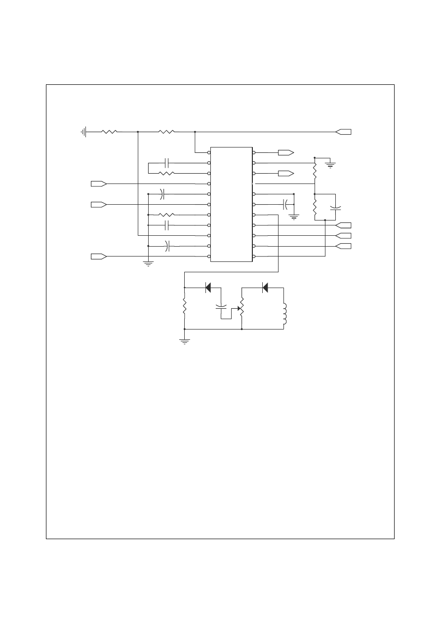
8. HOUSE KEEPING CIRCUIT
Using the KA3511 requires few external components to accomplish a complete housekeeping cir-
cuits for SMPS.
22
21
20
19
18
17
16
15
14
13
12
4
5
6
7
8
9
10
11
1
2
3
VCC
COMP
E/A(-)
E/A(+)
REM
RT
CT
DET
T
PG
PG
T
REM
C1
E
C2
DTC
GND
T
UVP
PT
V12
V5
V3.3
Vref
2k
Ω
(1W)
15k
Ω
0.01uF
12k
Ω
2.2uF
1uF
2.2uF
2k
Ω
(1W)
11k
Ω
33k
Ω
1.8k
Ω
0.1uF
1k
Ω
0.01uF
+
+
+
PG
Micom
12V
5V
Standby
Supply
V
CC
=20V
+
+
12V
5V
3V
K
A
3
5
1
1
19
Rev C, November 1999
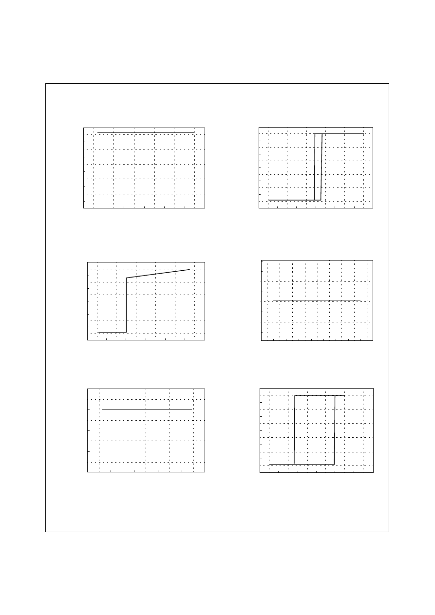
9. TYPICAL CHARACTERISTICS
V
CC
-I
CC
Bandgap Reference Voltage
PIN19(Dead Time Control Voltage)-Duty Cycle
OVP for 3.3V
OVP for 5V
OVP for 12V
Temperature Characteristic
0.014
0.012
0.010
0.008
0.006
0.004
0.002
0.000
0
10
20
30
40
Supply Voltage [V]
50
40
30
20
10
0
0.0
0.5
1.0
1.5
2.0
2.5
3.0
2.73
Deadtime Control Voltage [V]
7
6
5
4
3
2
1
0
5.0
5.5
6.0
6.5
7.0
I
CC
[
A
]
D
u
ty
R
a
tio
[%
]
31.1%
21.8%
12.8%
V5 [V]
5.010
5.008
5.006
5.004
5.002
-40
-20
0
20
40
60
80
100
120
140
TEMP [
°
C]
Vr
e
f [
V
]
V
PG
[V]
5
4
3
2
1
0
3.6
3.8
4.0
4.2
4.4
4.6
V3.3 [V]
V
PG
[V
]
5
4
3
2
1
0
14.0
14.2
14.4
14.6
14.8
15.0
V12 [V]
V
PG
[V]
20
Rev C, November 1999
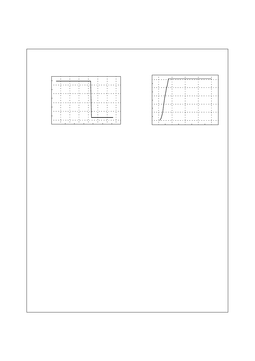
OVP for PT
UVP for 3.3V
UVP for 5V
UVP for 12V
Remote ON Charging Current
REM ON/OFF Vth
5
4
3
2
1
0
1.15
1.20
1.25
1.30
1.35
Vpt [V]
V
PG
[V
]
V
PG
[V]
Pin 13 (V3.3) Voltage [V]
5
4
3
2
1
0
21
22
23
24
25
V
PG
[V
]
5
4
3
2
1
0
3.6
3.8
4.0
4.2
4.4
4.6
4.8
5.0
Pin 14 (V5) Voltage [V]
Pin 15 (V12) Voltage [V]
5
4
3
2
1
0
9.0
9.5
10.0
10.5
11.0
V
PG
[V]
5
4
3
2
1
0
0
1
2
3
4
5
V
PG
[V
]
Vrem [V]
-0.000016
-0.000018
-0.000020
-0.000022
-0.000024
0
50
100
150
200
250
Ir
e
m
[
A]
21
Rev C, November 1999
Remote ON Open Voltage
Detecting V
CC
Voltage (DET)
Detecting V5 Voltage
Charging Current for PG
Short Circuit Current
Hysteresis Voltage 2
5
4
3
2
1
0
0
1
2
3
4
5
Vre
m
[
V]
V
PG
[
V]
5
4
3
2
1
0
1.0
1.1
1.2
1.3
1.4
1.5
-0.000005
-0.000010
-0.000015
-0.000020
0
20
40
60
80
100
120
140
160
I
PG
[V
]
5
4
3
2
1
0
4.0
4.2
4.4
4.6
4.8
5.0
Pin 14 (5V) Voltage [V]
V
PG
[V]
-0.032
-0.033
-0.034
-0.035
0
100
200
300
400
Ir
e
f [
A
]
5
4
3
2
1
0
0.0
0.5
1.0
1.5
2.0
2.5
V
PG
[
V]
Pin 9 (DET) Voltage [V]
Pin 10 (T
PG
) Voltage [V]
22
Rev C, November 1999
Error Amp Sink Current
Reference Voltage
0.002
0.00
-0.002
-0.004
-0.006
-0.008
0
20
40
60
80
100
120
140
Is
ink
&
I
s
ou
rc
e
[A
]
5
4
3
2
1
0
0
10
20
30
40
Vre
f [
V]
Supply Voltage [V]
23
Rev C, November 1999
10. PACKAGE DIMENSION
1
11
12
22
9.14
±
0.20
10.16
0.400
2.54
0.100
0.360
±
0.008
0~15
°
0.25
+0.10
–0.05
0.010
+0.004
–0.002
3.40
±
0.30
0.134
±
0.012
3.81
±
0.20
0.150
±
0.008
27.49
±
0.20
1.082
±
0.008
27.90
1.098
MAX
5.08
0.200
0.51
0.020
MAX
MIN
1.05
0.041
()
0.46
±
0.10
0.018
±
0.004
0.060
±
0.004
1.52
±
0.10
22-DIP-400
24
Rev C, November 1999
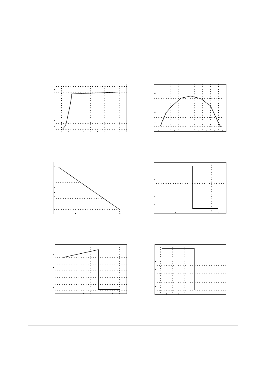
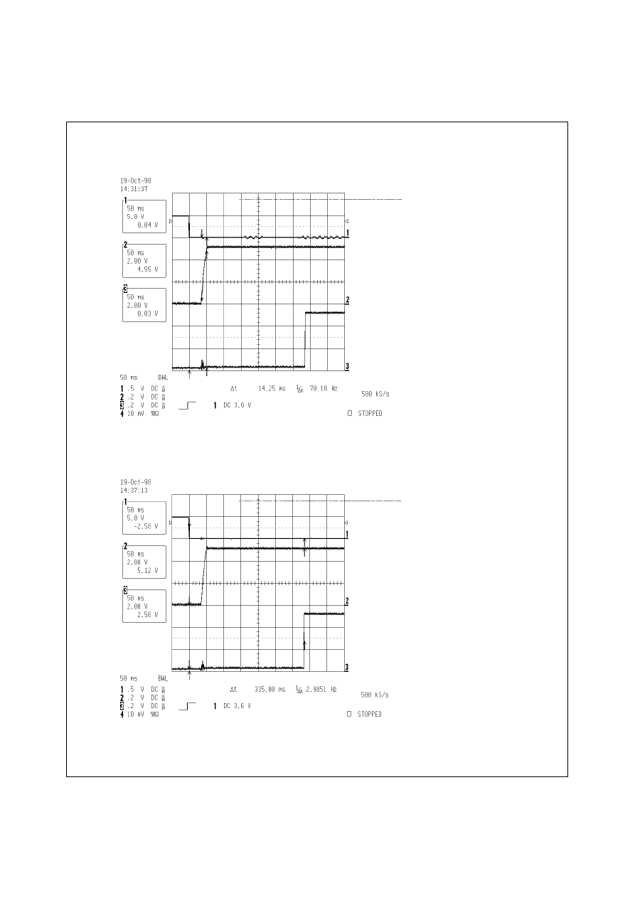
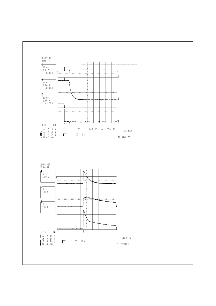
11. EXPERIMENTAL RESULT
Figure 12. Rising Time of +5Vdc Output Voltage
Figure 13. PG Signal Delay Time
CH1 : PS-ON
CH2 : +5Vdc Output
CH3 : PG Signal
CH1 : PS-ON
CH2 : +5Vdc Output
CH3 : PG Signal
25
Rev C, November 1999
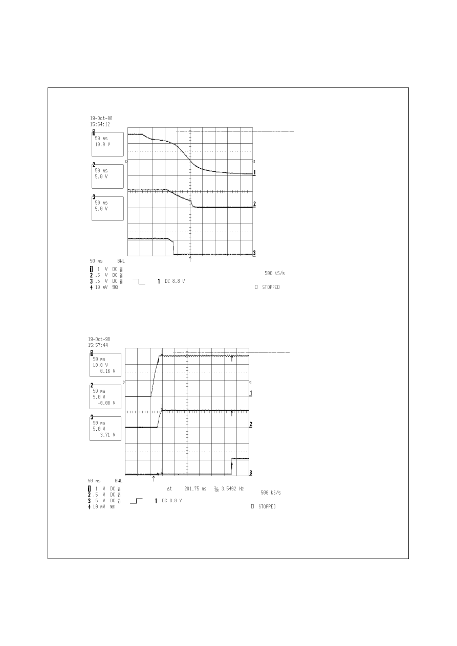
Figure 14. Power Down Warning
Figure 15. No Load Protection
CH1 : PS-ON
CH2 : +5Vdc Output
CH3 : PG Signal
CH1 : +3.3Vdc Output
CH2 : +5Vdc Output
CH3 : +12Vdc Output
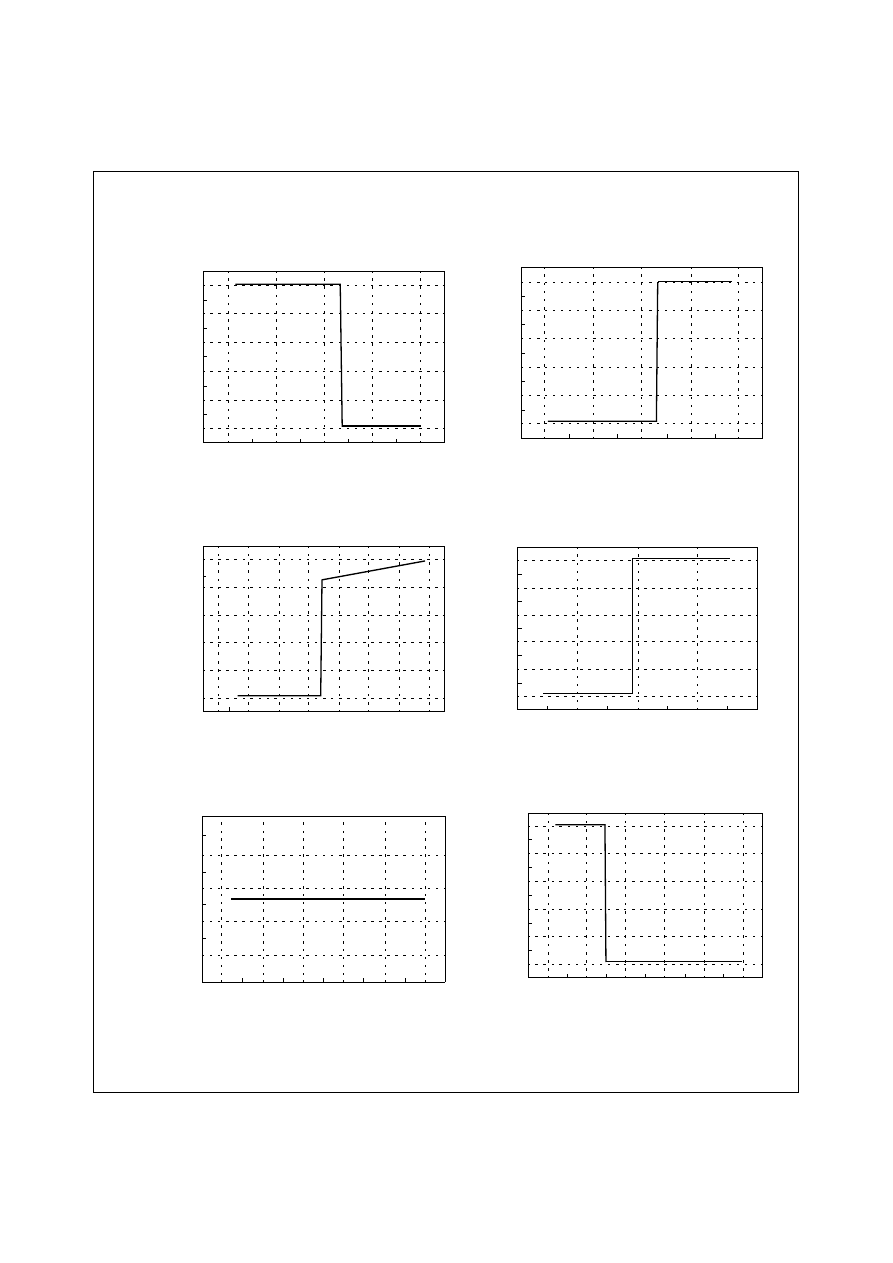
26
Rev C, November 1999
Figure 16. Vcc, +5Vdc Output vs. PG Signal (High)
Figure 16. Vcc, +5Vdc Output vs. PG Signal (Low)
CH1 : Vcc
CH2 : +5Vdc Output
CH3 : PG Signal
CH1 : Vcc
CH2 : +5Vdc Output
CH3 : PG Signal
27
Rev C, November 1999
12. APPLICATION CIRCUIT
Reference
1. Power Electronics by Marvin J. Fisher
2. Principles Of Power Electronics by Kassakian
AUTHOR:
Sang-Tae Im: P-IC Application Team
Tel. 82-32-680-1275
Fax. 82-32-680-1317
E-mail. sangtae.im@Fairchildsemi.co.kr
C6
22uF
+
2.2uF
+
IC1
AR3511X
Vcc
1
C1
22
COMP
2
E
21
E/A(-)
3
C2
20
DTC
19
E/A(+)
4
TREM
5
GND
18
REM
6
TUVP
17
RT
7
PT
16
CT
8
V12
15
DET
9
V5
14
TPG
10
V3.3
13
PG
11
Vref
12
CT
15K
R5
70K
R6
47K
R4
1.2K
R3
56K
100K
103
0.1uF
+
C16
+
2.2uF
+
103
D19
D9
VR1
5V OUT
12V OUT
POWER ON
OUT REF
PG
3.3V OUT
VCC
C1
C2

TRADEMARKS
ACEx™
CoolFET™
CROSSVOLT™
E
2
CMOS
TM
FACT™
FACT Quiet Series™
FAST
®
FASTr™
GTO™
HiSeC™
The following are registered and unregistered trademarks Fairchild Semiconductor owns or is authorized to use and is
not intended to be an exhaustive list of all such trademarks.
LIFE SUPPORT POLICY
FAIRCHILD’S PRODUCTS ARE NOT AUTHORIZED FOR USE AS CRITICAL COMPONENTS IN LIFE SUPPORT
DEVICES OR SYSTEMS WITHOUT THE EXPRESS WRITTEN APPROVAL OF FAIRCHILD SEMICONDUCTOR CORPORATION.
As used herein:
1. Life support devices or systems are devices or
systems which, (a) are intended for surgical implant into
the body, or (b) support or sustain life, or (c) whose
failure to perform when properly used in accordance
with instructions for use provided in the labeling, can be
reasonably expected to result in significant injury to the
user.
2. A critical component is any component of a life
support device or system whose failure to perform can
be reasonably expected to cause the failure of the life
support device or system, or to affect its safety or
effectiveness.
PRODUCT STATUS DEFINITIONS
Definition of Terms
Datasheet Identification
Product Status
Definition
Advance Information
Preliminary
No Identification Needed
Obsolete
This datasheet contains the design specifications for
product development. Specifications may change in
any manner without notice.
This datasheet contains preliminary data, and
supplementary data will be published at a later date.
Fairchild Semiconductor reserves the right to make
changes at any time without notice in order to improve
design.
This datasheet contains final specifications. Fairchild
Semiconductor reserves the right to make changes at
any time without notice in order to improve design.
This datasheet contains specifications on a product
that has been discontinued by Fairchild semiconductor.
The datasheet is printed for reference information only.
Formative or
In Design
First Production
Full Production
Not In Production
DISCLAIMER
FAIRCHILD SEMICONDUCTOR RESERVES THE RIGHT TO MAKE CHANGES WITHOUT FURTHER
NOTICE TO ANY PRODUCTS HEREIN TO IMPROVE RELIABILITY, FUNCTION OR DESIGN. FAIRCHILD
DOES NOT ASSUME ANY LIABILITY ARISING OUT OF THE APPLICATION OR USE OF ANY PRODUCT
OR CIRCUIT DESCRIBED HEREIN; NEITHER DOES IT CONVEY ANY LICENSE UNDER ITS PATENT
RIGHTS, NOR THE RIGHTS OF OTHERS.
TinyLogic™
UHC™
VCX™
ISOPLANAR™
MICROWIRE™
POP™
PowerTrench
QFET™
QS™
Quiet Series™
SuperSOT™-3
SuperSOT™-6
SuperSOT™-8
Wyszukiwarka
Podobne podstrony:
Fran Saleški Finžgar Dekla Ančka
NADCI NIENIE WROTNE, KA
Wykład 5 An wsk cz II
An%20Analysis%20of%20the%20Data%20Obtained%20from%20Ventilat
NLP for Beginners An Idiot Proof Guide to Neuro Linguistic Programming
02 01 11 11 01 44 an kol2 1 7id 3881
50 Common Birds An Illistrated Guide to 50 of the Most Common North American Birds
Ca ka niew a ciwa
więcej podobnych podstron