
Raman Spectrum of Graphene and Graphene Layers
A. C. Ferrari,
1,
J. C. Meyer,
2
V. Scardaci,
1
C. Casiraghi,
1
M. Lazzeri,
3
F. Mauri,
3
S. Piscanec,
1
D. Jiang,
4
K. S. Novoselov,
4
S. Roth,
2
and A. K. Geim
4
1
Cambridge University, Engineering Department, JJ Thompson Avenue, Cambridge CB3 0FA, United Kingdom
2
Max Planck Institute for Solid State Research, Stuttgart 70569, Germany
3
IMPMC, Universite´s Paris 6 et 7, CNRS, IPGP, 140 rue de Lourmel, 75015 Paris, France
4
Department of Physics and Astronomy, University of Manchester, Manchester, M13 9PL, United Kingdom
(Received 9 June 2006; published 30 October 2006)
Graphene is the two-dimensional building block for carbon allotropes of every other dimensionality.
We show that its electronic structure is captured in its Raman spectrum that clearly evolves with the
number of layers. The D peak second order changes in shape, width, and position for an increasing
number of layers, reflecting the change in the electron bands via a double resonant Raman process. The G
peak slightly down-shifts. This allows unambiguous, high-throughput, nondestructive identification of
graphene layers, which is critically lacking in this emerging research area.
DOI:
PACS numbers: 78.67.Bf, 63.20.Dj, 63.20.Kr, 78.30.j
The current interest in graphene can be attributed to
three main reasons. First, its electron transport is described
by the Dirac equation and this allows access to quantum
electrodynamics in a simple condensed matter experiment
[
]. Second, the scalability of graphene devices to nano-
dimensions [
–
] makes it a promising candidate for
applications, because of its ballistic transport at room
temperature combined with chemical and mechanical
stability. Remarkable properties extend to bilayer and
few-layers graphene [
]. Third, various forms of
graphite, nanotubes, buckyballs, and others can all be
viewed as derivatives of graphene and, not surprisingly,
this basic material has been intensively investigated theo-
retically for the past 60 years [
]. The recent discovery of
graphene [
] at last allows us to probe it experimentally,
which paves the way to better understanding the other
allotropes and to resolve controversies.
Graphene can be obtained using the procedure of
Ref. [
], i.e., micromechanical cleavage of graphite.
Alternative procedures, such as exfoliation and growth,
so far only produced multilayers [
], but it is hoped
that in the near future efficient growth methods will be
developed, as happened for nanotubes. Despite the wide
use of the micromechanical cleavage, the identification and
counting of graphene layers is a major hurdle. Monolayers
are a great minority amongst accompanying thicker flakes.
They cannot be seen in an optical microscope on most
substrates. They only become visible when deposited on
oxidized Si substrates with a finely tuned thickness of the
oxide layer (typically, 300 nm SiO
2
) since, in this case,
even a monolayer adds to the optical path of reflected light
to change the interference color with respect to the empty
substrate [
]. Atomic force microscopy (AFM) has been
so far the only method to identify single and few layers, but
it is low throughput. Moreover, due to the chemical con-
trast between graphene and the substrate (which results in
an apparent chemical thickness of 0.5–1 nm, much bigger
of what expected from the interlayer graphite spacing
[
]), in practice, it is only possible to distinguish between
one and two layers by AFM if films contain folds or
wrinkles [
]. This poses a major limitation to the range
of substrates and is a setback for the widespread utilization
of this material. Here, we show that graphene’s electronic
structure is uniquely captured in its Raman spectrum.
Raman fingerprints for single layers, bilayers, and few
layers reflect changes in the electron bands and allow
unambiguous, high-throughput, nondestructive identifica-
tion of graphene layers, which is critically lacking in this
emerging research area.
Here the samples are prepared by micromechanical
cleavage [
]. To provide the most definitive identification
of single and bilayers (beyond the AFM counting proce-
dure) we perform transmission electron microscopy (TEM)
on some of the samples to be measured by Raman spec-
troscopy. Samples for TEM are prepared following a simi-
lar process to that previously used to make freestanding
and TEM-compatible nanotube devices [
]. In addition,
this allows us to have freestanding layers on a grid easily
seen in an optical microscope, facilitating their location
during Raman measurements, Fig.
. Electron diffrac-
tion is done in a Zeiss 912 microscope at a voltage of
60 kV, and high-resolution images are obtained with a
Philips CM200 microscope at 120 kV. A high resolution-
TEM analysis of foldings at the edges or within the free-
hanging sheets gives the number of layers by direct visual-
ization, since at a folding the sheet is locally parallel to the
beam, Figs.
–
. Edges and foldings of one or two
layers are dominated by one or two dark lines, respectively.
The number of layers is also obtained by a diffraction
analysis of the freely suspended sheets for varying inci-
dence angles, and confirms the number of layers from the
foldings, Figs.
and
. In particular, the diffraction
analysis of the bilayer shows that it is A-B stacked (the
intensity of the 11– 20 diffraction spots (outer hexagon) is
roughly twice that of the 1–100 (inner hexagon), Fig.
,
in agreement with diffraction simulations obtained by a
PRL 97, 187401 (2006)
P H Y S I C A L
R E V I E W
L E T T E R S
week ending
3 NOVEMBER 2006
0031-9007= 06=97(18)=187401(4)
187401-1
© 2006 The American Physical Society
Fourier transform of projected atomic potentials. This
confirms our multilayer graphene has the same stacking
as graphite.
Raman spectra are measured on single, bi, and multi-
layers on Si SiO
2
. Some are then processed into free-
hanging sheets, as described above, and measured again
after TEM. The measurements are performed at room
temperature with a Renishaw spectrometer at 514 and
633 nm, with notch filters cutting at 100 cm
1
. A
100 objective is used. Extreme care is taken to avoid
sample damage or laser induced heating. Measurements
are performed from 4 to 0:04 mW incident power. No
significant spectral change is observed in this range. The
Raman spectra of suspended and on-substrate graphene are
similar, the main difference being a small D peak in the
TEM samples. We also measure the reference bulk graph-
ite used to produce the layers.
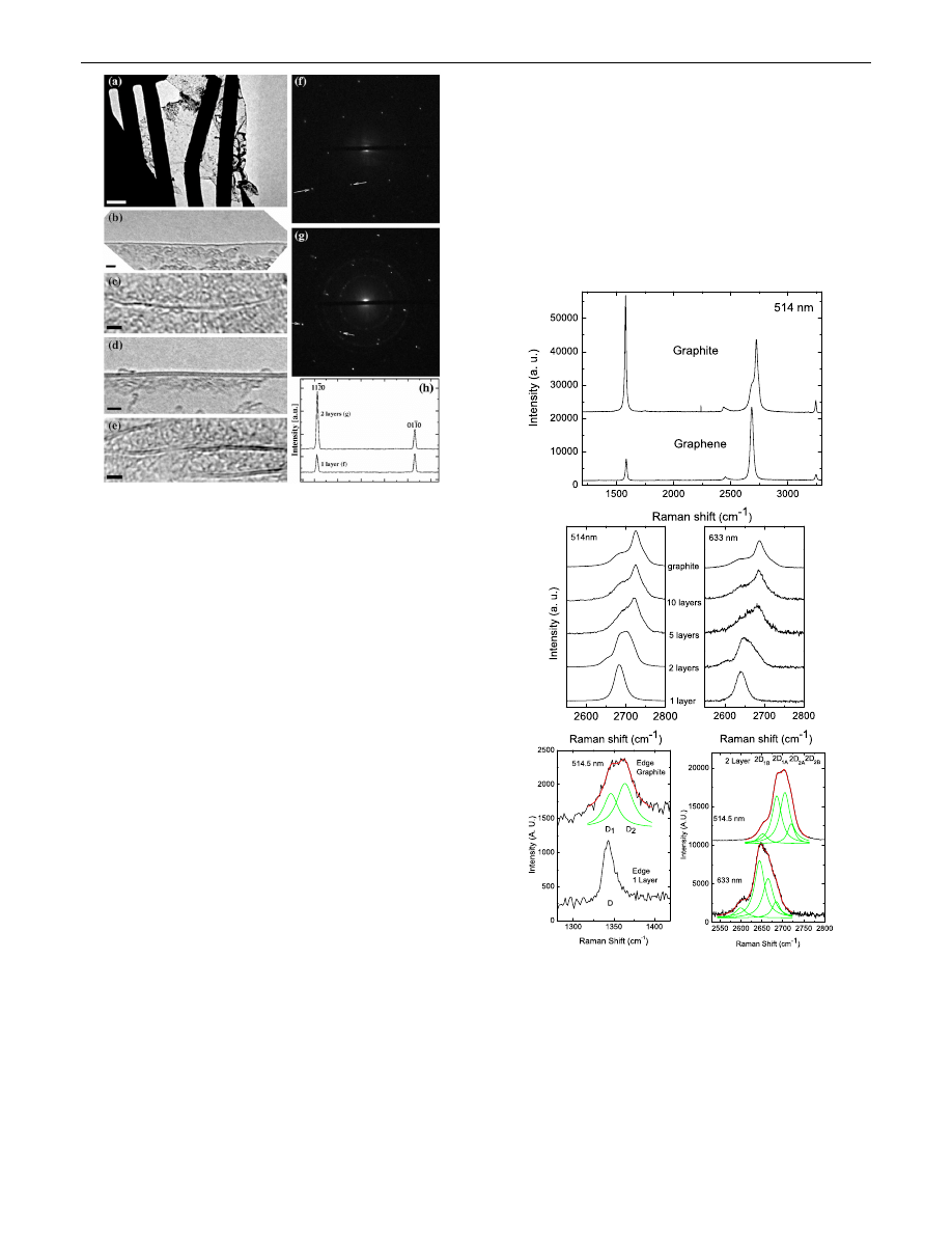
Figure
compares the 514 nm Raman spectra of
graphene and bulk graphite. The two most intense features
are the G peak at 1580 cm
1
and a band at 2700 cm
1
,
historically named G
0
, since it is the second most promi-
nent peak always observed in graphite samples [
]. The G
peak is due to the doubly degenerate zone center E
2g
mode
[
]. On the contrary, the G
0
band has nothing to do with
the G peak, but is the second order of zone-boundary
phonons. Since zone-boundary phonons do not satisfy the
Raman fundamental selection rule, they are not seen in first
order Raman spectra of defect-free graphite [
]. Such
phonons give rise to a peak at 1350 cm
1
in defected
graphite, called D peak [
]. Thus, for clarity, we refer to
(a)
(b)
(c)
(d)
(e)
FIG. 2 (color online).
(a) Comparison of Raman spectra at
514 nm for bulk graphite and graphene. They are scaled to
have similar height of the 2D peak at 2700 cm
1
. (b) Evolu-
tion of the spectra at 514 nm with the number of layers. (c) Evo-
lution of the Raman spectra at 633 nm with the number of layers.
(d) Comparison of the D band at 514 nm at the edge of bulk
graphite and single layer graphene. The fit of the D
1
and D
2
components of the D band of bulk graphite is shown. (e) The
four components of the 2D band in 2 layer graphene at 514 and
633 nm.
FIG. 1.
(a) TEM of suspended graphene. The grid is also
visible in optical microscopy. (b) High-resolution image of a
folded edge of a single layer and (c) a wrinkle within the layer.
(d) Folded edge of a two layer, and (e) internal foldings of the
two layer. The amorphous contrast on the sheets is most likely
due to hydrocarbon adsorbates on the samples that were cracked
by the electron beam. (f ) Electron diffraction pattern for close to
normal incidence from single layer and (g) from two layers.
Weak diffraction peaks from the supporting metal structure are
also present. (h) Intensity profile plot along the line indicated by
the arrows in (f ),(g). The relative intensities of the spots in the
two layer are consistent only with A-B (and not A-A) stacking.
Scale bars: (a) 500 nm; (b– e) 2 nm.
PRL 97, 187401 (2006)
P H Y S I C A L
R E V I E W
L E T T E R S
week ending
3 NOVEMBER 2006
187401-2
the G
0
peak as 2D. Figure
shows that no D peak is
observed in the center of graphene layers. This proves the
absence of a significant number of defects. As expected, a
D
peak is only observed at the sample edge, Fig.
Figure
shows a significant change in shape and inten-
sity of the 2D peak of graphene compared to bulk graphite.
The 2D peak in bulk graphite consists of two components
2D
1
and 2D
2
], roughly 1=4 and 1=2 the height of
the G peak, respectively. Here we measure a single, sharp
2D peak in graphene, roughly 4 times more intense than
the G peak. Notably, the G peak intensity of single layer
and bulk graphite is comparable [note that Fig.
is
rescaled to show a similar 2D intensity] and the G position
is 3–5 cm
1
higher than bulk graphite. This upshift is
partially due to chemical doping. The change in shape of
the 2D band is nicely confirmed in Fig.
, which com-
pares the D peak of the graphite edge with that of the
graphene edge. The graphene D peak is a single sharp
peak, while in graphite is a band consisting of two peaks
D
1
and D
2
[
]. Figures
and
plot the evolution of
the 2D band as a function of layers for 514.5 and 633 nm
excitations. These immediately indicate that a bilayer has a
much broader and up-shifted 2D band with respect to
graphene. This band is also quite different from bulk
graphite. It has 4 components, 2D
1B
, 2D
1A
, 2D
2A
, 2D
2B
;
two of which, 2D
1A
and 2D
2A
, have higher relative inten-
sities than the other two, as indicated in Fig.
Figure
and
show that a further increase in layers
leads to a significant decrease of the relative intensity of
the lower frequency 2D
1
peaks. For more than 5 layers the
Raman spectrum becomes hardly distinguishable from that
of bulk graphite. Thus Raman spectroscopy can clearly
distinguish a single layer, from a bilayer from few (less
than 5) layers. This also explains why previous experi-
ments on nanographites, but not single or bilayer graphene,
did not identify these features [
]. In particular, it was
noted from early studies that turbostratic graphite (i.e.,
without AB stacking) has a single 2D peak [
].
However, its full width at half maximum (FWHM) is
50 cm
1
almost double that of the 2D peak of graphene
and up-shifted of 20 cm
1
. Turbostratic graphite also often
has a first order D peak [
]. Single wall carbon nanotubes
(SWNTs) show a sharp 2D peak similar to that measured
here for graphene [
]. The close similarity (in position
and FWHM) of our measured graphene 2D peak and the
2D peak in SWNTs of 1– 2 nm diam [
] implies that
curvature effects are small for the 2D peak for SWNTs in
this diameter range, the most commonly found in experi-
ments. This questions the assumption that the 2D peak in
SWNT should scale to the up-shifted average 2D peak
position in bulk graphite for large diameters [
]. Thus
the scaling law relating diameter and 2D peak position,
often used to derive the inner diameter in double wall tubes
[
], needs to be revisited. Despite the similarities, there
are major differences between graphene and SWNT
Raman spectra, which allow us to easily distinguish
them. Indeed, confinement and curvature split the two
degenerate modes of the G peak in SWNTs [
], resulting
in G
and G
peaks.
We now explain why graphene has a single 2D peak, and
why this splits in four components in bilayer graphene.
Several authors previously attempted to explain the double
structure of the 2D peak in graphite [
], how-
ever they always neglected the evolution of the electronic
bands with the number of layers, which is, on the contrary,
the key fact. The 2D peak in graphene is due to two
phonons with opposite momentum in the highest optical
branch near the K (A
0
1
symmetry at K) [
]. Figure
shows that this peak changes in position with varying
excitation energy. This is due to a double resonance (DR)
process, which links the phonon wave vectors to the elec-
tronic band structure [
].
Within DR, Raman scattering is a fourth order process
involving four virtual transitions: (i) a laser induced exci-
tation of an electron-hole pair [a ! b vertical transition in
Fig.
]; (ii) electron-phonon scattering with an ex-
changed momentum q close to K (b ! c); (iii) electron-
phonon scattering with an exchanged momentum q (c !
b
); (iv) electron-hole recombination (b ! a). The DR
condition is reached when the energy is conserved in these
transitions. The resulting 2D Raman frequency is twice the
frequency of the scattering phonon, with q determined by
the DR condition. For simplicity, Figs.
and
ne-
glect the phonon energy and do not show the equivalent
processes for hole-phonon scattering. In addition, we only
consider the dispersions along K M K
0
.
The transitions within this line correspond to the peaks in
the phonon distribution fulfilling DR [
], once the trigo-
nal warping is considered [
ε
L
q
a
c
b
ε
L
q
1B
q
1A
ε
L
q
2A
q
2B
~ ~
~ ~
~ ~
Γ
K
M
K'
Electron energy
a) Monolayer:
b) Bilayer:
π
*
π
q = exchanged
phonon momentum
ε
L
= Laser energy
Fermi level
FIG. 3.
DR for the 2D peak in (a) single layer and (b) bilayer.
PRL 97, 187401 (2006)
P H Y S I C A L
R E V I E W
L E T T E R S
week ending
3 NOVEMBER 2006
187401-3

Consistent with the experimental observation of a single
component for the 2D peak in single layer graphene,
Figs.
and
only shows the phonon satisfying DR
conditions with momentum q > K, along the K M
direction (K < q < M). The other two possible DR pho-
nons, with q < K and q K, give a much smaller contri-
bution to the Raman intensity. In fact, the q < K phonon
involves a smaller portion of the phase space because of the
band-structure trigonal warping (see Figs. 3,4 of Ref. [
]
and related discussion) and the q K phonon has a zero
electron-phonon coupling for this transition, as discussed
in Ref. [
] (see footnote 24, for q K,
00
0) and
Ref. [
]. This differs from the model of Ref. [
], which
predicts 2 similar components for the D peak even in single
layer, in disagreement with the experiments of Fig.
We now examine the bilayer case. The observed 4 com-
ponents of the 2D peak could in principle be attributed to
two different mechanisms: the splitting of the phonon
branches [
], or the spitting of the electronic
bands [
]. To ascertain this we compute the phonon
frequencies [
] for both single and bilayer graphene
(stacked AB, as indicated by TEM), at the q corresponding
to the DR condition for the 514 and 633 nm lasers. The
splitting of the phonon branches is <1:5 cm
1
, much
smaller than the experimentally observed 2D splitting.
Thus, this is solely due to electronic bands effects. In the
bilayer, the interaction of the graphene planes causes the
and
bands to divide in four bands, with a different
splitting for electrons and holes, Fig.
. According to
the density functional theory (DFT) dipole matrix ele-
ments, amongst the 4 possible optical transitions, the inci-
dent light couples more strongly the two transitions shown
in Fig.
. The two almost degenerate phonons in the
highest optical branch couple all electron bands amongst
them. The resulting four processes involve phonons with
momenta q
1B
, q
1A
, q
2A
, and q
2B
, as shown in Fig.
. The
four corresponding processes for the holes, and those
associated to the 2 less intense optical transitions [not
shown in Fig.
], are associated to momenta almost
identical to q
1B
, q
1A
, q
2A
, q
2B
and almost (within
0:2 cm
1
) identical Raman shifts. These wave vectors
correspond to phonons with different frequencies, due to
the strong phonon dispersion around K induced by the
electron-phonon coupling [
]. They produce four differ-
ent peaks in the Raman spectrum of bilayer graphene.
Table
reports the expected splittings and shows that
they compare very well with experiments.
In conclusion, graphene’s electronic
structure is
uniquely captured in its Raman spectrum, that clearly
evolves with the number of layers. Raman fingerprints
for single-, bilayer, and few-layer graphene reflect changes
in the electronic structure and electron-phonon interactions
and allow unambiguous, high-throughput, nondestructive
identification of graphene layers.
A. C. F. acknowledges funding from EPSRC No. GR/
S97613, The Royal Society, and The Leverhulme Trust;
C. C. acknowledges funding from the Oppenheimer Fund.
Electronic address: acf26@eng.cam.ac.uk
[1] K. S. Novoselov et al., Proc. Natl. Acad. Sci. U.S.A. 102,
10 451 (2005).
[2] K. S. Novoselov et al., Nature (London) 438, 197 (2005).
[3] Y. Zhang et al., Nature (London) 438, 201 (2005).
[4] K. S. Novoselov et al., Science 306, 666 (2004).
[5] K. S. Novoselov et al., Nature Phys. 2, 177 (2006).
[6] Y. Zhang et al., Appl. Phys. Lett. 86, 073104 (2005).
[7] N. M. Peres et al., Phys. Rev. B 73, 125411 (2006).
[8] C. Berger et al., J. Phys. Chem. B 108, 19 912 (2004).
[9] K. Wakabayashi, Phys. Rev. B 64, 125428 (2001).
[10] K. Nakada et al., Phys. Rev. B 54, 17 954 (1996).
[11] J. Scott Bunch et al., Nano Lett. 5, 287 (2005).
[12] P. R. Wallace, Phys. Rev. 71, 622 (1947).
[13] L. M. Viculis, J. J. Mack, and R. B. Kaner, Science 299,
1361 (2003).
[14] J. C. Meyer et al., Ultramicroscopy 106, 176 (2006);
Science 309, 1539 (2005).
[15] R. P. Vidano et al., Solid State Commun. 39, 341 (1981).
[16] F. Tuinstra and J. Koenig, J. Chem. Phys. 53, 1126 (1970).
[17] R. J. Nemanich and S. A. Solin, Phys. Rev. B 20, 392
(1979).
[18] L. G. Cancado et al., Phys. Rev. Lett. 93, 047403 (2004).
[19] L. G. Cancado et al., Phys. Rev. B 66, 035415 (2002).
[20] P. Lespade et al., Carbon 22, 375 (1984).
[21] A. Jorio et al., Phys. Rev. B 66, 115411 (2002).
[22] A. G. Souza Filho et al., Phys. Rev. B 67, 035427 (2003).
[23] R. Pfeiffer et al., Phys. Rev. B 71, 155409 (2005).
[24] J. Maultzsch, S. Reich, and C. Thomsen, Phys. Rev. B 70,
155403 (2004).
[25] A. C. Ferrari and J. Robertson, Phys. Rev. B 61, 14 095
(2000).
[26] S. Piscanec et al., Phys. Rev. Lett. 93, 185503 (2004).
[27] C. Thomsen and S. Reich, Phys. Rev. Lett. 85, 5214 (2000).
[28] J. Kurti et al., Phys. Rev. B 65, 165433 (2002).
[29] A. C. Ferrari and J. Robertson, Phil. Trans. R. Soc. A 362,
2267 (2004).
TABLE I.
Relative splitting of 2D components in bilayer
graphene (in cm
1
). In each case, we show the shift with respect
to the average frequency of the two main peaks. The four
columns of the bilayer correspond to processes q
1B
, q
1A
, q
2A
,
q
2B
, respectively. The theoretical values are obtained by multi-
plying the DR q vectors determined from the DFT electronic
bands by dw=dq 645 cm
1
A. Here dw=dq is the ratio be-
tween the measured shift of the 2D peak frequency with the laser
energy in graphene (99 cm
1
=eV), and the corresponding
variation of the DR q 2k computed from the DFT bands.
514.5 nm
Experimental
44
10
10
25
Theory
44
11
11
41
633 nm
Experimental
55
10
10
30
Theory
44
9
9
41
PRL 97, 187401 (2006)
P H Y S I C A L
R E V I E W
L E T T E R S
week ending
3 NOVEMBER 2006
187401-4
Wyszukiwarka
Podobne podstrony:
41 Phys Rev Lett 97 016801 2006
24 Phys Rev Lett 99 216802 2007
32 Phys Rev Lett 98 196806 2007
51 Phys Rev Lett 92 237001 2004
20 Phys Rev Lett 100 016602 2008
39 Phys Rev B 74 064403 2006
57 Phys Rev B 67 054506 2003
25 Appl Rev Lett 91 233108 2007 Nieznany (2)
11 Phys Rev B 78 085432 2008id Nieznany (2)
48 Phys Rev B 72 024537 2005
27 Phys Rev B 76 081406R 2007
14 Phys Rev B 77 233406 2008
46 Phys Rev B 72 Rapid Commun 201401 2005
5 Phys Rev B 79 115441 2009
43 Appl Phys Lett 88 013901 200 Nieznany (2)
więcej podobnych podstron