LETTERS
Breakdown of the adiabatic
Born–Oppenheimer approximation
in graphene
SIMONE PISANA
1
, MICHELE LAZZERI
2
, CINZIA CASIRAGHI
1
, KOSTYA S. NOVOSELOV
3
, A. K. GEIM
3
,
ANDREA C. FERRARI
1
* AND FRANCESCO MAURI
2
*
1
Engineering Department, Cambridge University, Cambridge CB3 0FA, UK
2
IMPMC, Universit ´es Paris 6 et 7, CNRS, IPGP, 140 rue de Lourmel, 75015 Paris, France
3
Department of Physics and Astronomy, University of Manchester, Manchester M13 9PL, UK
*
e-mail: acf26@eng.cam.ac.uk; francesco.mauri@impmc.jussieu.fr
Published online: 11 February 2007; doi:10.1038/nmat1846
The
adiabatic
Born–Oppenheimer
approximation
(ABO)
has been the standard ansatz to describe the interaction
between electrons and nuclei since the early days of quantum
mechanics
1,2
. ABO assumes that the lighter electrons adjust
adiabatically to the motion of the heavier nuclei, remaining
at any time in their instantaneous ground state. ABO is well
justified when the energy gap between ground and excited
electronic states is larger than the energy scale of the nuclear
motion. In metals, the gap is zero and phenomena beyond
ABO (such as phonon-mediated superconductivity or phonon-
induced renormalization of the electronic properties) occur
3
.
The use of ABO to describe lattice motion in metals is, therefore,
questionable
4,5
. In spite of this, ABO has proved e
ffective for
the accurate determination of chemical reactions
6
, molecular
dynamics
7,8
and phonon frequencies
9–11
in a wide range of
metallic systems. Here, we show that ABO fails in graphene.
Graphene, recently discovered in the free state
12,13
, is a zero-
bandgap semiconductor
14
that becomes a metal if the Fermi
energy is tuned applying a gate voltage
13,15
,
V
g
. This induces
a sti
ffening of the Raman G peak that cannot be described
within ABO.
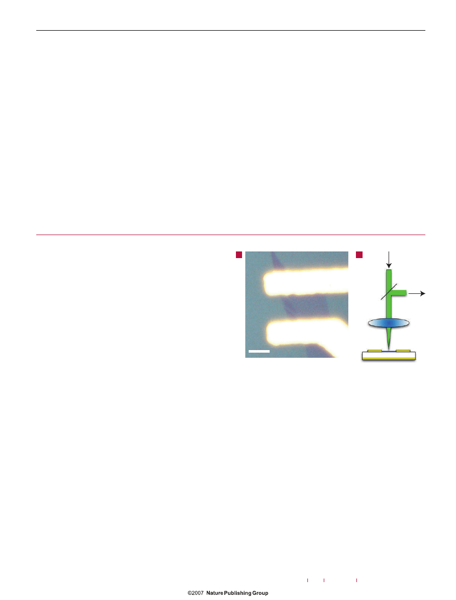
Graphene samples are prepared by micromechanical cleavage
of bulk graphite at the surface of an oxidized Si wafer with
a 300-nm-thick oxide layer, following the procedures described
in ref. 12. This allows us to obtain graphene monocrystals
exceeding 30
μ
m in size, Fig. 1a. Using photolithography, we then
make Au/Cr electrical contacts, which allow the application of a
gate voltage,
V
g
, between the Si wafer and graphene (Fig. 1a,b).
The resulting devices are characterized by electric-field-e
ffect
measurements
13,15,16
, yielding a charge-carrier mobility,
μ
, of
5,000–10,000 cm
2
V
−1
s
−1
at 295 K and a zero-bias (
V
g
=
0)
doping of
∼
10
12
cm
−2
. This is reflected in the existence of
a finite gate voltage,
V
n
, at which the Hall resistance is
zero and the longitudinal resistivity reaches its maximum.
Accordingly, a positive (negative)
V
g
–
V
n
induces electron (hole)
doping, having an excess-electron surface concentration of
n
= η(V
g
− V
n
)
. The coe
fficient
η ≈
7
.
2
×
10
10
cm
−2
V
−1
is found
from Hall e
ffect measurements and agrees with the geometry of the
resulting capacitor
12,13,15
.
From Ar
laser (514 nm)
To spectrometer
×50 objective
Back gate
5
5
μm
a
b
Source
Drain
Figure 1
Experimental set-up. a, Optical micrograph of the contacted graphene
sample. b, Schematic diagram of the Raman and transport set-up. The laser spot
size is
∼1 μm
2
.
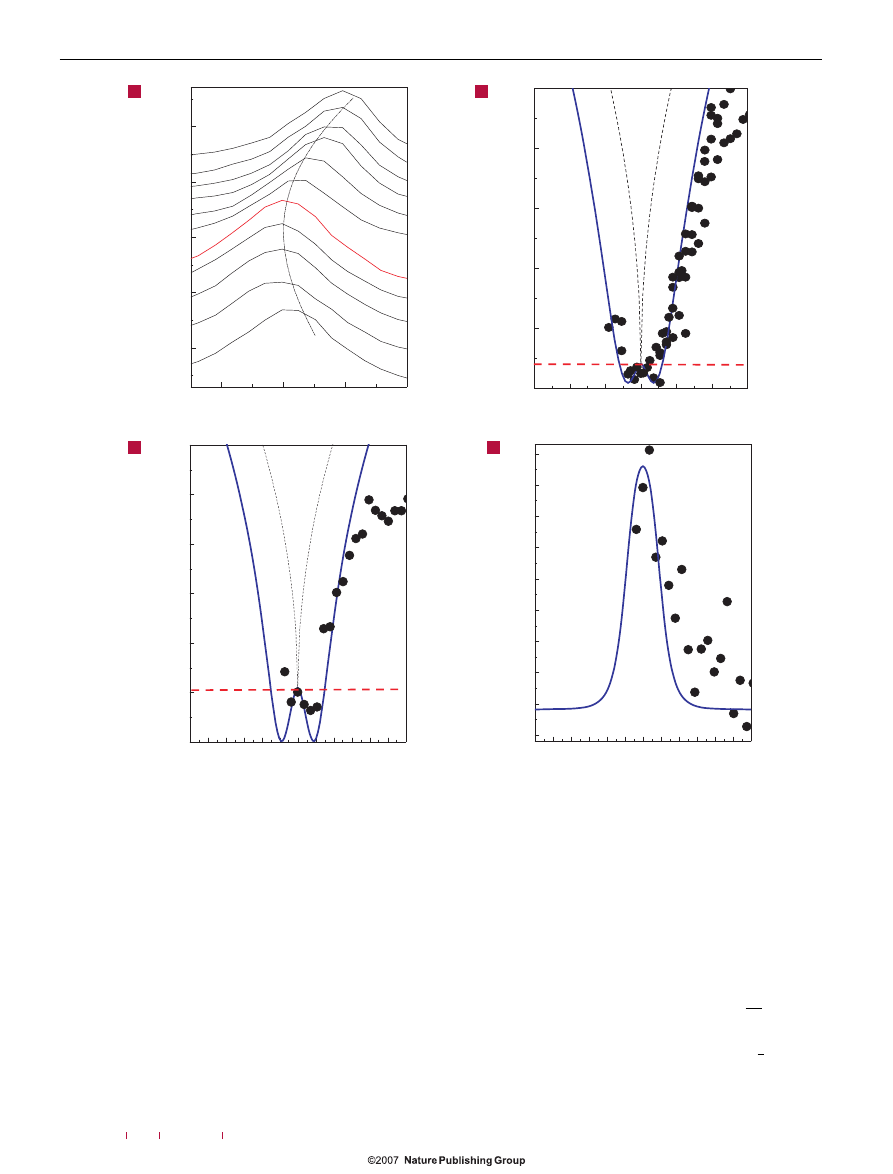
Unpolarized Raman spectra are measured at 295 and 200 K in
ambient air and in vacuum (
<
5
×
10
−6
mbar), respectively, with
a Renishaw spectrometer at 514 nm using a
×
50 long-working-
distance objective, Fig. 1b. The incident power is kept well below
4 mW to avoid sample damage or laser-induced heating
17
. The
Raman spectra are measured as a function of the applied
V
g
, Fig. 2a.
Each spectrum is collected for 30 s. The applied gate voltage tends
to move
V
n
, especially at room temperature. We thus determine
the
V
g
corresponding to the minimum G-peak position, and use
this to estimate
V
n
. The G peak upshifts with positive applied
V
g
–
V
n
at room temperature (Fig. 2a,b) and at 200 K (Fig. 2c). A
similar trend, albeit over a smaller voltage range, is observed for
negative
V
g
–
V
n
. This upshift for both electron and hole doping is
qualitatively similar to that reported by Yan
et al.
for electrically
doped graphene measured at 10 K (ref. 18).
The Raman G peak of graphene corresponds to the E
2g
phonon
at the Brillouin zone centre,
, (refs 17,19). Phonon calculations
for undoped graphene and graphite show the presence of a Kohn
198
nature
materials
VOL 6 MARCH 2007 www.nature.com/naturematerials
Untitled-3 1
9/2/07, 7:58:33 pm
LETTERS
1,580
1,585
1,590
1,595
Intensity (a.u.)
–20 V
–10 V
0 V
20 V
10 V
30 V
40 V
50 V
60 V
70 V
80 V
–6
–4
–2
0
1,584
1,585
1,586
1,587
1,588
1,589
2
4
6
Raman shift (cm
–1
)
Raman shift (cm
–1
)
Raman shift (cm
–1
)
Electron concentration (10
12
cm
–2
)
Electron concentration (10
12
cm
–2
)
Electron concentration (10
12
cm
–2
)
–6 –5 –4 –3 –2 –1
0
1
2
3
4
5
6
–6 –5 –4 –3 –2 –1
0
1
2
3
4
5
6
7
8
9
10
11
12
13
14
15
16
FWHM(G)
1,587
1,588
1,589
1,590
1,591
1,592
1,593
a
b
d
c
Figure 2
Raman G peak of doped graphene. a, Measurements at 295 K as a function of V
g
. The red spectrum corresponds to the undoped case. b,c, G-peak position as a
function of electron concentration at 295 K (b) and 200 K (c). Black circles: measurements; red dashed line: adiabatic Born–Oppenheimer; blue line: finite-temperature
non-adiabatic calculation from equation (6); black dashed line: simplified non-adiabatic calculation from equation (5). The minimum observed in the calculations at
∼10
12
cm
−2
occurs when the Fermi energy equals half of the phonon energy. d, FWHM(G) at 200 K as a function of electron concentration. Circles: measures; blue line:
theoretical FWHM of a Voigt profile obtained from a lorentzian component given by equation (7) and a constant gaussian component of
∼8 cm
−1
.
anomaly in the phonon dispersion of the E
2g
mode near
(ref. 20).
A Kohn anomaly is the softening of a phonon of wavevector q
∼
2k
F
,
where k
F
is a Fermi-surface wavevector. By doping graphene, the
change in the Fermi surface moves the Kohn anomaly away from
q
=
0. Thus, as Raman spectroscopy probes phonons with q
=
0,
intuitively we could expect a sti
ffening of the q
=
0 G peak. This
would be in agreement with our experiments. To validate this
picture, we need to compute the frequency of the E
2g
mode in
doped graphene.
In graphene, the electronic bands near the high-symmetry K
points are well described by a Dirac dispersion
14
(
k
,π
∗
) = ¯hv
F
k
and
(
k
,π) = −¯hv
F
k
, where k
+
K is the momentum of the Dirac
Fermions,
v
F
is the Fermi velocity and
¯hv
F
=
5
.
52 eV ˚
A, from
density functional theory (DFT)
20
(Fig. 3a). The Dirac point is
defined by the crossing of these conic bands and coincides with
K, Fig. 3a. Thus, at zero temperature, the doping-induced shift of
the Fermi level from the Dirac point is
F
=
sgn
(n)
√
n
π¯hv
F
, where
sgn
(x)
is the sign of
x
.
The E
2g
phonon in graphene consists of an in-plane
displacement of the carbon atoms by a vector
±
u
/
√
2 as shown
in Fig. 3d. In the presence of such atomic displacements, the bands
are still described by a cone (that is, a gap does not open) with the
nature
materials
VOL 6 MARCH 2007 www.nature.com/naturematerials
199
Untitled-3 2
9/2/07, 7:58:36 pm
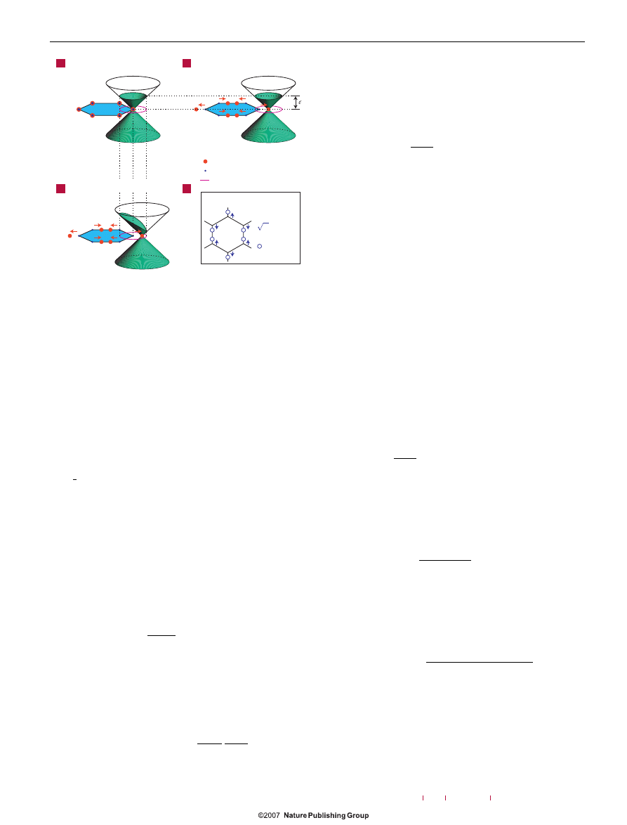
LETTERS
s = 0
BZ
s
s
Non adiabatic
Unperturbed
Adiabatic
BZ: Brillouin zone
Dirac points
K points
Fermi surface
u/
2
C atoms
Real space
π
π
a
b
c
d
*
F
Figure 3
Schematic
π band structure of doped graphene near the
high-symmetry K point of the Brillouin zone. The filled electronic states are
shown in green. a, Bands of the perfect crystal. The Dirac point is at K, the
electronic states are filled up to the Fermi energy
F
and the Fermi surface is a circle
centred at K. b, Bands in the presence of an E
2g
lattice distortion. The Dirac points
are displaced from K by
±s. Within ABO, the electrons remain in the instantaneous
ground state: the bands are filled up to
F
and the Fermi surface follows the
Dirac-point displacement. The total electron energy does not depend on s. c, Bands
in the presence of an E
2g
lattice distortion. In the non-adiabatic case, the electrons
do not have time to relax their momenta (through impurity, electron–electron and
electron–phonon scattering) to follow the instantaneous ground state. In the
absence of scattering, the electron momentum is conserved and a state with
momentum k is occupied if the state with the same k is occupied in the unperturbed
case. As a consequence, the Fermi surface is the same as in the unperturbed case
and does not follow the Dirac-cone displacement. The total electron energy
increases with s
2
, resulting in the observed E
2g
-phonon stiffening. d, Atomic pattern
of the E
2g
phonon. The atoms are displaced from the equilibrium positions by
±u/
√
2. Note that the displacement pattern of the Dirac points (in reciprocal space)
is identical to the displacement pattern of the carbon atoms (in real space).
Dirac point shifted from K by a vector s (Fig. 3b,c)
21
. In practice, the
atomic pattern of the E
2g
vibrations is mirrored into an identical
pattern of Dirac-point vibrations in the reciprocal space. The
dependence of the electronic bands on u can be obtained from the
DFT electron–phonon coupling matrix elements (see equation (6)
and note 24 of ref. 20 and Supplementary Information):
(
k
,π
∗
/π,
u
) = ±¯hv
F
|
k
−
s
(
u
)|
(1)
where s
·
u
=
0,
s
= u
2
D
2
F
/(¯hv
F
)
and
D
2
F
=
45
.
6 eV
2
˚
A
−2
is the deformation potential of the E
2g
mode
22
. Equation (1) well
reproduces the modification of the DFT band structure of graphene
owing to a static displacement (frozen phonon) of the atoms
according to the G phonon pattern.
The knowledge of the electronic bands (in the presence of a
phonon) allows the determination of the phonon energy
¯hω
F
as
a function of
F
. In particular,
¯hω = ¯hω
F
− ¯hω
0
=
¯h
2
M
ω
0
d
2
E
(
d
u
)
2
,
(2)
where
M
is the carbon mass,
ω
0
is the frequency in the undoped
case,
ω ω
0
and
E
is the variation of the electronic energy
with
F
.
Within ABO,
E(u)
is computed assuming a static atomic
displacement. Under this hypothesis, for any given displacement u,
the electrons are supposed to be in the ground state, that is, the
bands are filled up to
F
(Fig. 3b). Thus, the adiabatic
E
is
E(u) =
4
A
(
2
π
2
)
(k,π
∗
,u)<
F
(
k
,π
∗
,
u
)
d
2
k
,
(3)
where we consider
F
>
0,
A
=
5
.
24 ˚
A
2
is the unit-cell area and a
factor of 4 accounts for spin and K-point degeneracy. Combining
equations (1) and (3), we find that
E
does not depend on u
and
¯hω =
0. Thus, within ABO, the Raman G-peak position is
independent of
F
, in contrast with experiments, Fig. 2b,c.
This failure of the frozen-phonon calculation urges us to
re-examine the assumptions underlying ABO. The E
2g
phonon
is a dynamical perturbation described by a time-dependent
lattice displacement
˜
u
(t) =
u cos
(ω
0
t
)
oscillating at the G-peak
frequency. Within ABO, it is assumed that, at any given time
t
,
the electrons are in the adiabatic ground state of the instantaneous
band structure
(
k
,π
∗
, ˜
u
(t))
. However, the inverse of the G-
peak pulsation is
∼
3 fs, which is much smaller than the typical
electron-momentum relaxation times
τ
m
(owing to impurity,
electron–electron and electron–phonon scattering with non-zero
momentum phonons). Indeed, a
τ
m
of a few hundred femtoseconds
is deduced from the electron mobility in graphene
23
and from
ultrafast spectroscopy in graphite
24,25
. As a consequence, the
electrons do not have time to relax their momenta to reach the
instantaneous adiabatic ground state, as assumed in ABO. The
departure from the adiabatic ground state can be accounted for in
the calculation of
E
, by filling the perturbed bands,
(
k
,π
∗
,
u
)
with the occupations of the unperturbed bands
(
k
,π
∗
,
0
)
, as
in Fig. 3c:
E(u) =
4
A
(
2
π
2
)
(k,π
∗
,0)<
F
(
k
,π
∗
,
u
)
d
2
k
+
O
(u
3
).
(4)
This equation is valid in the limit
F
¯hω
0
/
2, and can be
rigorously derived using time-dependent perturbation theory,
as shown in the Supplementary Information. In this case,
the non-adiabatic energy,
E
, depends on
u
. Combining
equations (1), (4) and (2) and carrying out the integral we get:
¯hω =
¯hAD
2
F
πMω
0
(¯hv
F
)
2
|
F
| = α
|
F
|,
(5)
where
α
=
4
.
39
×
10
−3
.
The result of equation (5) can be extended to any
F
and finite
temperature
T
by computing the real part of the phonon self-
energy
3
with the DFT electron–phonon coupling matrix elements
(equation (6) and note 24 of ref. 20) to obtain:
¯hω = α
P
∞
−∞
[f ( −
F
) − f ()]
2
sgn
()
2
− (¯hω
0
)
2
/
4
d
,
(6)
where P is the principal part and
f
is the Fermi–Dirac distribution
at
T
(refs 26–28). Figure 2b,c show the excellent agreement of
our non-adiabatic finite
T
calculation (equation (6)) with the
experiments. The measured trends are also well captured by the
simplified model, equation (5). By comparing the adiabatic and
non-adiabatic calculations, we conclude that the sti
ffening of
the E
2g
mode with
|
F
|
is due to the departure of the electron
population from the adiabatic ground state.
200
nature
materials
VOL 6 MARCH 2007 www.nature.com/naturematerials
Untitled-3 3
9/2/07, 7:58:40 pm
LETTERS
A pictorial interpretation of this phenomenon (valid for
F
¯hω
0
/
2) can be obtained by considering what happens to
a filled glass when shaken horizontally. The liquid gravitational
energy and its level mimic the electronic energy
E
and
F
,
respectively. The shaking frequency mimics the phonon frequency
and the relaxation time of the liquid surface mimics the electron
relaxation time. If the motion of the glass is slow, the liquid surface
remains flat and its gravitational energy is independent of the glass
horizontal position, as in equation (3) and in Fig. 3b. If the motion
of the glass is rapid, the liquid surface profile is not flat and its
gravitational energy increases with the displacement of the glass,
as in equation (4) and Fig. 3c. To push the analogy even further,
a non-cylindrical glass should be used, where the liquid surface
increases with the liquid level. In this case, the higher the liquid
level, the larger the di
fference between the gravitational energies in
the fast- and slow-shaken glasses. Indeed, in graphene, the higher
the Fermi level, the larger the di
fference between the non-adiabatic
E
and the adiabatic
E
. This causes the observed sti
ffening of the
phonon frequency with
F
.
The validity of our model is further confirmed by the analysis of
the G-peak linewidth. The phonon decaying into an electron–hole
pair gives the most important contribution to the homogeneous
broadening of the E
2g
phonon. The full-width at half-maximum
(FWHM),
γ
, can be computed extending to finite
T
and
F
=
0 the
results of ref. 22:
γ =
π
2
ω
0
α
c
f
− ¯
h
ω
0
2
−
F
− f
¯hω
0
2
−
F
,
(7)
where
c
is the speed of light. At
T
=
0,
γ =
11 cm
−1
for
F
=
0
and
γ
drops to zero for
F
> ¯hω
0
/
2 because the scattering process
is forbidden by the Pauli exclusion principle
22
. Figure 2d shows a
good agreement between the experimental and theoretical
γ
, once a
constant inhomogeneous gaussian broadening of
∼
8 cm
−1
is added
to the electron–phonon contribution of equation (7).
In summary, graphene is a remarkable example of ABO
violation. Within ABO, the energy of a zone-centre phonon is
determined by two contributions: the distortion of the electronic
bands, associated with the phonon displacement, and the adiabatic
rearrangement of the Fermi surface. In graphene, these two
contributions cancel out exactly because of the peculiar rigid
motion of the Dirac cones, associated with the E
2g
phonon.
In general, a correct phonon treatment should not include
the adiabatic rearrangement of the Fermi surface whenever the
electron-momentum relaxation time is longer than the inverse
of the phonon pulsation, as occurs in graphene and in several
metals (see, for example, Table 1.3 of ref. 29). Note that the
stronger the electron–phonon coupling with q
=
0 phonons, the
larger the di
fference between ABO and non-ABO frequencies.
However, the lattice dynamics is well described by ABO if the
electron–phonon coupling with q
=
0 phonons is so strong that
the electron-momentum relaxation is faster than the lattice motion.
We anticipate that the ABO breakdown described here will
a
ffect the vibrational properties of carbon nanotubes
30
and
phonon-mediated superconductors. Furthermore, the resulting
variation of the Raman active peaks in graphene and nanotubes can
allow determination of the e
ffective doping by Raman spectroscopy,
with important consequences for basic and applied research.
Received 29 November 2006; accepted 18 January 2007; published 11 February 2007.
References
1. Born, M. & Oppenheimer, J. R. Zur quantentheorie der molekeln.
Ann. Phys.
84, 457–484 (1927).
2. Ziman, J. M.
Electrons and Phonons
(Oxford Univ. Press, Oxford, 1960).
3. Grimvall, G.
The Electron-Phonon Interaction in Metals
(North-Holland, Amsterdam, 1981).
4. Ponosov, Y. S., Bolotin, G. A., Thomsen, C. & Cardona, M. Raman scattering in Os: Nonadiabatic
renormalization of the optical phonon self energies.
Phys. Status Solidi B
208, 257–269 (1988).
5. White, J. D., Chen, J., Matsiev, D., Auerbach, D. J. & Wodtke, A. M. Conversion of large-amplitude
vibration to electron excitation at a metal surface.
Nature
433, 503–505 (2005).
6. Kroes, G. J., Gross, A., Baerends, E. J., Sche
ffler, M. & McCormack, D. A. Quantum theory of
dissociative chemisorption on metal surfaces.
Acc. Chem. Res.
35, 193–200 (2002).
7. Alfe, D., Gillan, M. J. & Price, G. D. The melting curve of iron at the pressures of the Earth’s core from
ab initio
calculations.
Nature
401, 462–464 (1999).
8. Walker, B. G., Molteni, C. & Marzari, N. Ab initio molecular dynamics of metal surfaces.
J. Phys.
Condens. Matter
16, S2575–S2596 (2004).
9. Chester, G. V. The theory of interaction of electrons with lattice vibrations in metals.
Adv. Phys.
10,
357–400 (1961).
10. Baroni, S., De Gironcoli, S., Dal Corso, A. & Giannozzi, P. Phonons and related crystal properties
from density functional perturbation theory.
Rev. Mod. Phys.
73, 515–562 (2001).
11. Savrasov, S. Y. & Savrasov, D. Y. Electron-phonon interactions and related physical properties of
metals from linear-response theory.
Phys. Rev. B
54, 16487–16501 (1996).
12. Novoselov, K. S.
et al
. Two dimensional atomic crystals.
Proc. Natl Acad. Sci. USA
102,
10451–10453 (2005).
13. Novoselov, K. S.
et al
. Electric field e
ffect in atomically thin carbon films.
Science
306, 666–669 (2004).
14. Wallace, P. R. The band theory of graphite.
Phys. Rev.
71, 622–634 (1947).
15. Novoselov, K. S.
et al
. Two dimensional gas of massless Dirac fermions in graphene.
Nature
438,
197–200 (2005).
16. Zhang, Y., Tan, Y. W., Stormer, H. L. & Kim, P. Experimental observation of the quantum Hall e
ffect
and Berry’s phase in graphene.
Nature
438, 201–204 (2005).
17. Ferrari, A. C.
et al
. Raman spectrum of graphene and graphene layers.
Phys. Rev. Lett.
97,
187401 (2006).
18. Yan, J., Zhang, Y., Kim, P. & Pinczuk, A. Electric field e
ffect tuning of electron-phonon coupling in
graphene. Preprint at
<
http://www.arxiv.org/cond-mat/0612634
>
(2006).
19. Tuinstra, F. & Koenig, J. Raman spectrum of graphite.
J. Chem. Phys.
53, 1126–1130 (1970).
20. Piscanec, S., Lazzeri, M., Mauri, F., Ferrari, A. C. & Robertson, J. Kohn anomalies and electron
phonon interactions in graphite.
Phys. Rev. Lett.
93, 185503 (2004).
21. Dubay, O. & Kresse, G. Accurate density functional calculations for the phonon dispersion relations
of graphite layer and carbon nanotubes.
Phys. Rev. B
67, 035401 (2003).
22. Lazzeri, M., Piscanec, S., Mauri, F., Ferrari, A. C. & Robertson, J. Phonon linewidths and
electron-phonon coupling in graphite and nanotubes.
Phys. Rev. B
73, 155426 (2006).
23. Zhang, Y.
et al
. Landau-level splitting in graphene in high magnetic fields.
Phys. Rev. Lett.
96,
136806 (2006).
24. Moos, G., Gahl, C., Fasel, R., Wolf, M. & Hertel, T. Anisotropy of quasiparticle lifetimes and the role
of disorder in graphite from ultrafast time-resolved photoemission spectroscopy.
Phys. Rev. Lett.
87,
267402 (2001).
25. Kampfrath, T., Perfetti, L., Schapper, F., Frischkorn, C. & Wolf, M. Strongly coupled optical phonons
in the ultrafast dynamics of electronic energy and current relaxation in graphite.
Phys. Rev. Lett.
95,
187403 (2005).
26. Lazzeri, M. & Mauri, F. Non-adiabatic Kohn-anomaly in a doped graphene monolayer.
Phys. Rev.
Lett.
97, 266407 (2006).
27. Ando, T. Anomaly of optical phonon in monolayer graphene.
J. Phys. Soc. Jpn.
75, 124701 (2006).
28. Castro Neto, A. H. & Guinea, F. Electron-phonon coupling and Raman spectroscopy in graphene.
Phys. Rev. B
75, 045404 (2007).
29. Ashcroft, N. W. & Mermin, N. D.
Solid State Physics
(Saunders College, London, 1976).
30. Piscanec, S., Lazzeri, M., Robertson, J., Ferrari, A. C. & Mauri, F. Optical phonons in carbon
nanotubes: Kohn anomalies, peierls distortions and dynamic e
ffects.
Phys. Rev. B
75, 035427 (2007).
Acknowledgements
The authors thank P. Kim and A. Pinczuk for useful discussions and for sending us a preprint of
ref. 18. A.C.F. acknowledges funding from the Royal Society and The Leverhulme Trust. The
calculations were carried out at IDRIS (Orsay).
Correspondence and requests for materials should be addressed to A.C.F or F.M.
Supplementary Information accompanies this paper on www.nature.com/naturematerials.
Competing financial interests
The authors declare that they have no competing financial interests.
Reprints and permission information is available online at http://npg.nature.com/reprintsandpermissions/
nature
materials
VOL 6 MARCH 2007 www.nature.com/naturematerials
201
Untitled-3 4
9/2/07, 7:58:44 pm
Wyszukiwarka
Podobne podstrony:
materiałożnawstwo 9 - 08.05.2007, Materiałoznawstwo - wykłady
Materiałoznawstwo 03.12.2007, Materiałoznastwo
materiałoznawstwo 4 - 13.03.2007, Materiałoznawstwo - wykłady
30 Nature Mater 6 652 655 2007 Nieznany (2)
SŁ-34, WAT-materiały, saper
materiałoznawstwo 7 - 03.04.2007, Materiałoznawstwo - wykłady
metodologia 198 201
materiałoznawstwo 3 - 06.03.2007, Materiałoznawstwo - wykłady
fizyka 201 sprawko, I semstr moje materiały, fizyka, 201
materiałoznawstwo 6 - 27.03.2007, Materiałoznawstwo - wykłady
materiałoznastwo 26.11.2007, Materiałoznastwo
30 Nature Mater 6 652 655 2007
34 36 307cc pol ed02 2007
34 35 308 pol ed01 2007
34 35 307 pol ed02 2007
materiałoznawstwo 5 20 03 2007
34 35 307sw pol ed02 2007
więcej podobnych podstron