1
Supplementary reading - Common emitter amplifier
Course Website: http://www.radioelectronicschool.com
The purpose of this reading is to explain more about transistor bias and why a
common emitter (CE) amplifier produces a 180 degree phase change to the input
signal. Understanding this will give a better understanding of transistor operation –
particularly how ‘bias’ works. We will be looking at a BJT (Bipolar Junction
Transistor) in this reading but do kept in mind a CE amplifier can be made with any
other active device.
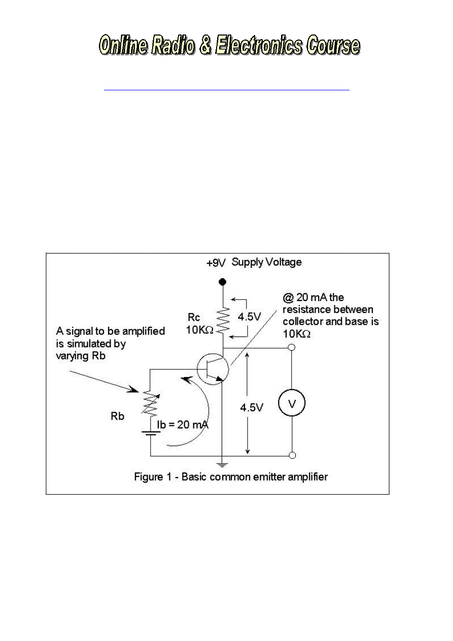
Figure 1 shows a simplified diagram of a CE amplifier.
Now the values that I have placed on the diagram in figure 1 are totally arbitrary and
at the same time realistic. What the actual operating voltages and currents are for a
particular transistor would be determined by referring the manufactures data sheets.
In figure one the base current is supplied by a separate battery and a resistor Rb. The
amount of base current (Ib) can be changed by varying Rb.

2
The collector of the transistor is connected to +9V via Rc. Though not shown the
emitter is connect to the negative side of the 9 volt supply.
So there are two supply voltages in this diagram – the bias voltage and the main
supply voltage of 9 volts. Can you tell if this transistor is connected the correct way
in this circuit in terms of the battery voltages?
Both power supplies have their negative terminal connected to earth (or the emitter).
What I do to determine if a transistor is drawn correctly is; I imagine I am an electron
coming from negative of each power supply and see if “I” have to flow
against the
arrow in the transistor symbol
to get to “my” positive side of the supply.
In figure 1 electrons must flow from earth (-9V) up into the emitter against the arrow
to get to the +9V at the collector. The other supply shown is a bias voltage supplied
by a battery. In the base circuit electrons flow from the negative terminal of this
battery against the arrow and back to the positive terminal. The battery voltages are
connected with the correct polarity to make this NPN transistor operate.
Now I have chosen an arbitrary value of 20mA for the base current. Accept this value
of base current for now. The base-emitter junction is forward biased and 20 mA of
base current is flowing. Since the base-emitter junction is forward biased – current
will also flow from the emitter through the transistor – out of the collector – then
through Rc and back to the +9V.
Since the emitter-collector circuit is in series with Rc then the sum of the voltage
drops across them must equal the supply voltage of 9 volts. Again I have arbitrarily
chosen an equal voltage across each. Half the supply voltage (4.5V) is across Rc and
the other half (another 4.5V) is across CE – the emitter and collector.
If 4.5 volts is across Rc and 4.5V is across the emitter-collector of the transistor
then;
in this circuit with this amount of base current flowing (20mA) the transistor
could be replaced with just a 10K resistor.
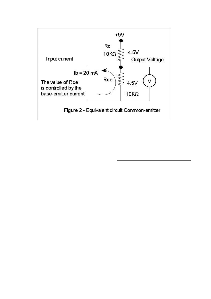
Figure 2 below shows an even more simplified (though very true) representation of
the circuit in figure 1. The transistor has been replaced with a 10K
Ω
resistor. In fact
a BJT really is a
current variable resistance
or
a resistor whose resistance is
determined by a current (the bias current).
The original name first given to a
transistor by its inventors was a
transfer resistor.
Have a look at figure 2.
3
I have replaced the transistor with a resistance of 10K. This 10K resistor represents
the resistance of the emitter-collector circuit. The resistance of the emitter-collector
circuit can be changed by changing the bias current (now at 20mA). If more bias
current were made to flow then the emitter-collector resistance of the BJT would fall
and less voltage would appear across it. The sum of the voltage drop across the
emitter-collector and Rc must always equal the applied voltage (9V).
So if the bias current were to increase – the emitter-collector resistance would
decrease and the voltage measure from the collector to ground (emitter) would fall
and the voltage across Rc would rise by the same amount.
If we were to decrease the bias current then the emitter-collector resistance would
increase. If the effective emitter-collector resistance rose above 10K then more
voltage would have to be measured on the voltmeter. If the emitter-collector
resistance increases then the emitter-collector voltage (as measured by the meter) will
rise and the voltage across Rc will decrease by the same amount. (the sum remaining
9V).
The transistor used in the common emitter configuration is really just two resistors in
series as shown in figure 2. However the resistance of the transistor (between
collector and emitter) is determined by the base-emitter current. Now – recall – the
signal to be amplified is connected to the base-emitter circuit. The amplifier output is
taken from the collector-emitter – or if you prefer – the output is taken from the
collector and ground.
4
The way a transistor amplifies (irrespective of its configuration CE, CB, or CC) is
that small changes is base-emitter current brings about large changes of emitter-
collector current.
Can you see that larger current is brought about by decreasing
resistance?.
You will be doing well right now if you can see that the transistor is really like a
special resistor whose resistance is controlled by an input current.
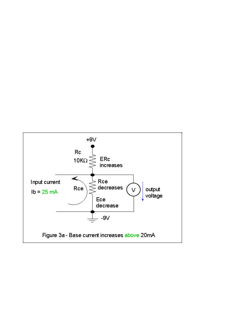
Have a look at figure 3a – we are not concerned about ‘absolute’ values of current
and voltage here as that will vary from transistor to transistor.
In figure 3a I have increased the base-emitter current. This means the transistor is
turned on harder. It also means its collector-emitter resistance Rce will decrease. The
output voltage across Rce or between the collector and ground must decrease.
The voltage across Rc i.e. ERc increases by the same amount that Ece decreases as
their sum must equal the supply voltage at all times.
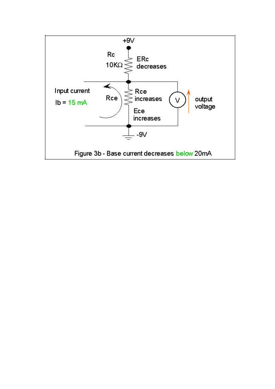
In figure 3b the base current is decreased. This means that the transistor will not
conduct from emitter to collector as hard – the transistor is being turned towards off
– its (the transistors) effective resistance between collector and emitter increase and
the voltage Ece must therefore increase.
When the transistor is left alone its base current will return to 20mA and the voltage
5
across Rce will return to 4.5V.
In a practical circuit this normal fixed value of the base current is called the bias or
quiescent base current. We don’t have a separate battery to supply bias. We also feed
our input signal to be amplified to the base-emitter circuit. The input signal will
either add to or subtract from the quiescent bias current. A resulting amplified output
voltage will appear between the collector of the common emitter amplifier and
ground.
You can see that the transistor needs DC voltages and currents in its quiescent state.
The signal to be amplified may well be AC or varying DC – it does not matter. A
capacitor passes AC or varying DC (well at least it appears to anyway). So capacitors
called coupling capacitors are added to the input and output circuits. Coupling
capacitors allow a varying current or voltage to be fed to and taken from the circuit
whilst blocking the DC voltages from the transistor affecting the previous and
subsequent stages.
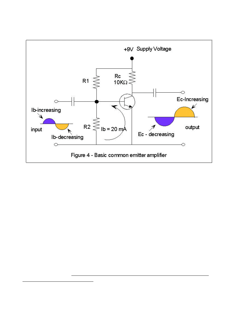
Have a look at figure 4.
This is actually a practical amplifier. The amount of quiescent base current (the bias)
is determined by the voltage divider consisting of R1 and R2. As before I have
arbitrarily chosen a transistor that requires a bias current of 20mA.
I have added input and output coupling capacitors.
6
The output voltage is taken from between the collector and ground and the circuit
operation is as described above.
An input signal that increases the base current (makes the base more positive with
respect to the emitter for NPN) will cause the output voltage to fall as shown in blue.
A input signal which causes the base current to decrease will cause the output voltage
to rise.
So you can see
that the amplified output is 180 degrees out of phase with the input
.
This phase shift is of no consequence when its comes to the intelligence or
information contained in the signal being amplified. The phase change matters when
we use feedback in circuits though this is an advanced topic. The output of the CE
amplifier if fed back to the input would be ‘negative feedback’.
I am often asked what the purpose of Rc is. If Rc were not present; firstly too much
emitter collector current would flow and the transistor would be destroyed. As
important; without Rc there would be no output – if we removed Rc and connect the
collector to the +9V supply then the voltage between emitter and collector would
always remained 9V. Rc is essential as it forms a voltage divider with the internal
resistance of the transistor (Rce). Changes in signal cause Rce to change in resistance
and the voltage change thereby produced across Rce is the output voltage.

7
We could add an emitter resistance (Re) to this circuit – as discussed in the reading
on semiconductors a small resistance in the emitter lead (say 1K in this circuit) will
prevent thermal runaway. If we do add a emitter resistance we also add an emitter
bypass capacitor across Re. The reactance of the bypass capacitor is typically 1/10
th
the resistance of Re at the lowest operating frequency.
Okay – well you should now see why a CE amplifier cause a 180 degree phase shift
and you should also have more of an understanding of transistor bias.
There are simple design formulas for choosing all the values in a CE amplifier like
all other amplifiers. You also would need access the data tables of the transistor. In
practice 99% of the time experimenters, hobbyists and even engineers work from
existing circuits – why recalculate the circuit when one is available.
Can you tell if the applied voltages to the circuit are correct. The examiner may
reverse a polarity and expect to see this – for example in the above circuit –9V could
be connected to the collector.
Can you identify the active device used? Can you identify that it is a CE circuit?
Identify voltage divider bias? Emitter stabilisation and bypassing. To lessor extent be
aware that there is a 180 degree phase change between output and input in a CE
amplifier. CE amplifiers have a relatively low input impedance and a moderately
high output impedance – the low input impedance is usually well suited for many
microphones used in radio communications and electronics.
Last revised 11 September 2000
Free for non-commercial use but must not be published without permission.
Copyright © 1999-2001 Ron Bertrand VK2DQ
Email: ron@radioelectronicschool.com
Wyszukiwarka
Podobne podstrony:
(Ebook) Radio & Electronics Course 81 Power Supply 12 Volt 3 Amp
Heathkit Basic Electricity Course (Basic radio Pt 2) ek 2b WW
Heathkit Basic Electricity Course (Basic radio Pt 2) ek 2b WW
Heathkit Basic Electricity Course (Basic radio Pt 2) ek 2b WW
Heathkit Basic Electricity Course (Basic transistors) ek 3 WW
Heathkit Basic Electricity Course (Basic transistors) ek 3 WW
Radio Electric Diagram
04 The Routledge Introductory Persian Course Supplement
Optional Supplemental Readings for Jon and Jonathan’s Wedding
US Army Electronics Course Basic Oscilloscope Od1402
Creating a live online radio station version 0 1
End course reading test 2
Mid course reading test 1
Electronics A Complete Course 2nd Ed
Mid course reading test 2
Course Readings
End course reading test 1
(ebook electronics) Schematics Power Regulated Power Supply for CB & Ham Radio
(Ebook Science) Stephen Covey The Speed Reading Course
więcej podobnych podstron