3935
3
The A3935 is designed specifically for automotive applications that
require high-power motors. The A3935 provides six high-current gate drive
outputs capable of driving a wide range of power n-channel MOSFETs.
A requirement of automotive systems is steady operation over a
varying battery input range. The A3935 integrates a pulse frequency
modulated boost converter to create a constant supply voltage for driving
the external MOSFETs. Bootstrap capacitors are utilized to provide the
above battery supply voltage required for n-channel MOSFETs.
Direct control of each gate output is possible via six TTL-compatible
inputs. A differential amplifier is integrated to allow accurate measurement of
the current in the three-phase bridge.
A diagnostic output can be continuously monitored to protect the
driver from short-to-battery, short-to-supply, bridge-open, and battery
under/overvoltage conditions. Additional protection features include dead-
time, VDD undervoltage, and thermal shutdown.
FEATURES
Drives Wide Range of N-Channel
MOSFETs in 3-Phase Bridges
PFM Boost Converter for Use With
Low-Voltage Battery Supplies
Internal LDO Regulator for Gate-
Driver Supply
Bootstrap Circuits for High-Side Gate
Drivers
Current Monitor Output
Adjustable Battery Overvoltage
Detection.
Diagnostic Outputs
Motor Lead Short-to-Battery,
Short-to-Ground, and Bridge-Open
Protection
Undervoltage Protection
-40
°
C to 150
°
C, T
J
Operation
Thermal Shutdown
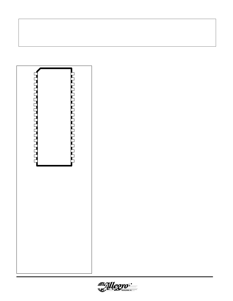
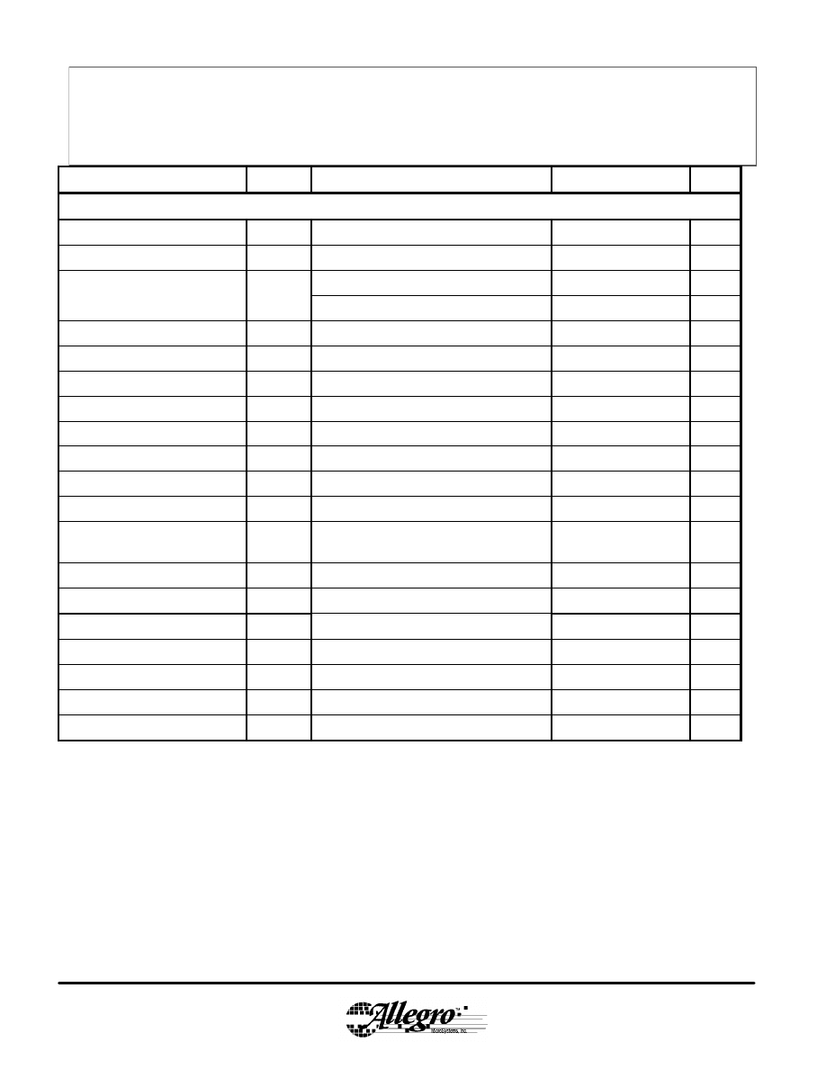
4
3
2
1
5
12
11
10
9
33
34
35
36
29
32
25
26
27
28
VDSTH
CSP
LSS
GLC
SC
SB
GHB
CB
GLA
CSOUT
OVSET
CSN
VDD
ALO
~ FAULT
BHI
AHI
BLO
ENABLE
A3935
K
LQ
15
14
13
SA
GHA
CA
18
17
16
VREG
VDRAIN
VBOOST
8
7
6
GHC
CC
GLB
31
30 CLO
CHI
22
23
24
UVFLT
VBAT
OVFLT
19
20
21
BOOSTD
BOOSTS
GND
[44-pin, PLCC pkg. ED also available]
ABSOLUTE MAXIMUM RATINGS
Load Supply Voltages, VBAT, VDRAIN
,
VBOOST, BOOSTD
………………
40 V
GHA/GHB/GHC, V
GHX
…………… -4 to 55 V
SA/SB/SC, V
SX
………………... -4 to 40 V
GLA/GLB/GLC, V
GLX
…………… -4 to 16 V
CSP,CSN, LSS …………………… -4 to 6.5 V
CA/CB/CC, V
CX
…………… -0.6 to 55 V
Logic Supply Voltage, V
DD
…… - 0.3 V to 6.5 V
Logic Input/Outputs and OVSET, BOOSTS,
CSOUT, VDSTH ………… -0.3 V to 6.5 V
Package Thermal Impedances (TA = +25
°
C)
ED pkg:
Θ
JA (JEDEC Hi-K PCB) …...
23
°
C/W
LQ pkg:
Θ
JA (JEDEC Hi-K PCB) …….
44
°
C/W
Operating Ambient Temperature Range,
T
A
……………….. -40
°
C to +135
°
C
Operating Junction Temperature Range,
T
J
............................. -40
°
C to +150
°
C
Storage Temperature Range,
T
S
............................ -55
°
C to +150
°
C
ADVANCED DATA SHEET –- 8/29/02
AUTOMOTIVE POWER-
MOSFET CONTROLLER
3935
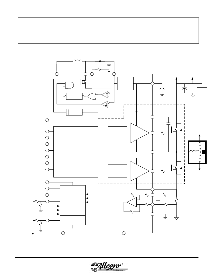
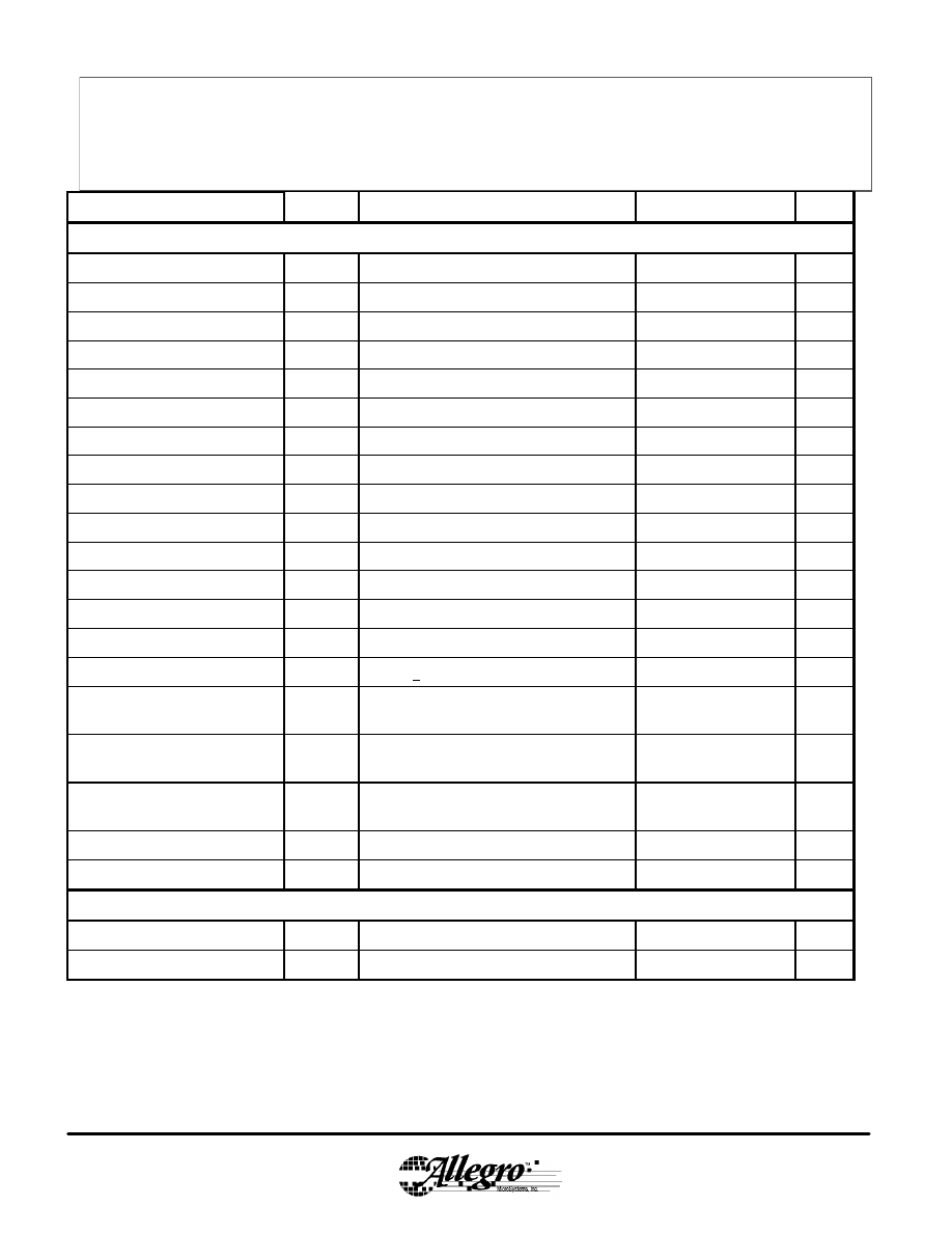
Automotive Power-MOSFET Controller
Functional Block Diagram (1 of 3 outputs shown)
VREG
High Side
Driver
Low Side
Driver
Turn ON
Delay
CA
GHA
SA
GLA
LSS
CSN
To Phase B
C
BOOT
To Phase C
Turn ON
Delay
R
SENSE
VBOOST
VBAT
-
+
Control
Logic
CSP
BOOSTS
BOOSTD
AHI
ALO
BHI
BLO
CHI
CLO
ENABLE
GND
cs
Drain-Source
Fault Monitor
VBAT Overvoltage
VBAT Undervoltage
VREG Undervoltage
Short to Ground
Short to Battery
Bridge Open
VDD Undervoltage
Thermal Shutdown
VDSTH
SA
SB
SC
CSOUT
VDRAIN
Low Drop
Out
Linear
Regulator
VREG
OS (off)
bi
bv
LSS
VDRAIN
(KELVIN)
OS (blank)
~ FAULT
Motor
Supply
Voltage
UVFLT
OVFLT
OVSET
VDD
Phase A
3935
VBAT
VIGN
VBAT
VREG
VDD
VDD
External +5V

3935
Automotive Power-MOSFET Controller
Terminal
Descriptions
AHI/BHI/CHI.
Direct control of high-side gate outputs
GHA/GHB/GHC. Logic “1” drives the gate “on”. Logic ”0”
pulls the gate down, turning off the external power
MOSFET. Internally pulled down when terminal is open.
ALO/BLO/CLO.
Direct control of low-side gate outputs
GLA/GLB/GLC. Logic “1” drives the gate “on”. Logic ”0”
pulls the gate down, turning off the external power
MOSFET
.
Internally pulled down when terminal is open.
BOOSTD.
Boost converter switch drain connection.
BOOSTS.
Boost converter switch source connection
CA/CB/CC.
High-side connection for bootstrap capacitor,
positive supply for high-side gate drive. The bootstrap
capacitor is charged to VREG when the output Sx terminal is
Low. When the output swings High, the voltage on this pin
rises with the output to provide the boosted gate voltage
needed for n-channel power MOSFETs.
CSN.
Input for current-sense, differential amplifier,
inverting, negative side. Kelvin connection for ground side
of current-sense resistor.
CSOUT.
Amplifier output voltage proportional to current
sensed across an external low-value resistor placed in the
ground-side of the power MOSFET bridge.
CSP.
Input for current-sense differential amplifier, non-
inverting, positive side. Connected to positive side of sense
resistor.
ENABLE
. Logic “0” disables the gate control signals and
switches off all the gate drivers “low” causing a “Coast”.
Can be used in conjunction with the gate inputs to PWM the
load current. Internally pulled down when terminal is open.
FAULT
\
.
Diagnostic logic output signal indicates that one
or more fault conditions has occurred, when “Low”.
GHA/GHB/GHC.
High-side gate drive outputs for n-ch
MOSFET drivers. External series gate resistors can control
slew rate seen at the power driver gate; thereby, controlling
the di/dt and dv/dt of Sx outputs.
GLA/GLB/GLC.
Low-side gate drive outputs for
external, n-channel MOSFET drivers. External series gate
resistors can control slew rate
GND.
Ground or negative side of VDD and VBAT
supplies.
LSS.
Low-side gate driver returns. Connects to the
common sources in the low-side of the power MOSFET
bridge.
OVFLT.
Logic “1” means that the VBAT exceeded the
VBAT overvoltage trip point set by OVSET level. It will
recover after a hysteresis below that maximum value. Has a
Hi-Z state.
OVSET.
A positive, dc level that controls the VBAT
Overvoltage trip point. Usually, provided from precision
resistor divider network between VDD and GND, but can be
held grounded for a preset value. When terminal is open sets
unspecified but high overvoltage trip point.
SA/SB/SC.
Directly connected to the motor terminals,
these pins sense the voltages switched across the load and
are connected to the negative side of the bootstrap
capacitors. Also, are the negative supply connection for the
floating, high-side drivers.
UVFLT.
Logic “1” means that VBAT is below its minimum
value and will recover after a hysteresis above that minimum
value. Has a Hi-Z state. [If UVFLT and OVFLT are both in
Hi-Z state; then, at least, a Thermal shutdown or VDD
Undervoltage has occurred.]
VBAT.
Battery voltage, positive input and is usually
connected to the motor voltage supply.
VBOOST.
Boost converter output, nominally 16 V, is also
input to regulator for VREG. Has internal boost current and
boost voltage control loops. In high-voltage systems is
approximately one diode drop below VBAT.
VDD.
Logic supply, positive side.
VDRAIN
. Kelvin connection for drain-to-source voltage
monitor and is connected to high-side drains of MOSFET
bridge. High Z when pin is open and registers as a short-to-
ground fault on all motor phases.
VDSTH
. A positive, dc level that sets the drain-to-source
monitor threshold voltage. Internally pulled down when
terminal is open.
VREG.
High-side, gate-driver supply, nominally, 13.5 V.
Has low-voltage dropout (LDO) feature.
3935
Automotive Power-MOSFET Controller
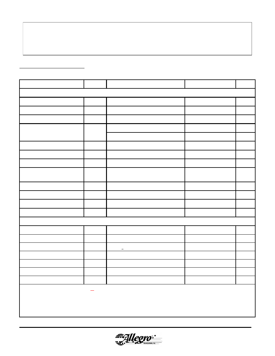
ELECTRICAL CHARACTERISTICS
(unless noted
; -40°C < Tj < 150°C, 7V < V
BAT
< 16 V, 4.75V < V
DD
< 5.25V, ENABLE =
22.5 kHz, 50% Duty cycle, two phases active. (*) or Typ. for design guide, only. Neg. current flows out of designated pin.)
Characteristics
Symbol
Test Conditions
Min.
Typ.
Max.
Units
Power Supply
V
DD
Supply Current
I
DD
All logic inputs = 0 V.
7
mA
V
BAT
Supply Current
I
BAT
All logic inputs = 0 V.
3
mA
Battery Voltage Operating Range
V
BAT
See Absolute Maximum Ratings.
7
40
V
I
DBOOT
= 10 mA
0.8
2
V
Bootstrap Diode Forward Voltage
V
DBOOT
I
DBOOT
= 100 mA
1.5
2.3
V
Bootstrap Diode Resistance
r
DBOOT
r
D
(100
mA)=[V
D
(150) -V
D
(50]/100
2.5
7.5
Ω
Bootstrap Diode Current Limit
I
LIM
3
V < [V
REG
– V
CX
] < 12
V
-150
-900
mA
Bootstrap Quiescent Current
I
CX
V
CX
= 40V, GHx = ON
10
30
uA
Bootstrap Refresh Time *
t
REFRESH
V
SX
= LOW to guarantee
∆
V=+0.5
V refresh of
0.47 uF Boot Cap at Vcx –Vsx = +10
V.
2.0
u
s
VREG Output Voltage
1
V
REG
VBAT=7
V to 40
V, Vboost from Boost Reg.
12.7
14
V
VREG Dropout Voltage
2
V
REGDO
V
REGDO
= Vboost – Vreg, Ireg = 40 mA
-
0.9
-
V
Gate Drive Avg. Supply Current *
I
REG
No external
dc
load at Vreg. Creg=10
uF.
40
mA
VREG Input Bias Current
I
REGBIAS
Current into VBOOST, ENABLE = 0.
4
mA
Boost Supply
V
BOOST
Output Voltage Limit
V
BOOSTLIM
VBAT = 7
V
14.9
16.3
V
V
BOOST
Output Volt. Limit Hysteresis
V
HYST
35
180
mV
Boost Switch ON
r
DS
(on)
I
BOOSTD
< 300
mA.
1.4
3.3
Ω
Max. Boost Switch Current
I
BOOST_SW
300
mA
Boost Current Limit Threshold Volt.
V
BI
Increasing V
BOOSTS
0.45
0.55
V
OFF Time
t
OFF
3
8
uS
Blanking Time
t
BLANK
100
220
nS
Footnotes: 1) For Vboostlim < Vboost < 40
V power dissipation in the Vreg LDO increases. Observe Tj < 150°C limit.
2) With Vboost decreasing Dropout Voltage measured at VREG = VREGref – 200
mV where VREGref = VREG at
Vboost= 16
V.
3935
Automotive Power-MOSFET Controller
Characteristics
Symbol
Test Conditions
Min.
Typ.
Max.
Units
Control Logic
V
IN
(1)
Minimum high level input for logical “one”.
2.0
–
–
V
Logic Input Voltages
V
IN
(0)
Maximum low level input for logical “zero”.
–
–
.8
V
I
IN
(1)
V
IN
= V
DD
–
500
µA
Logic Input Currents
I
IN
(0)
V
IN
= 0.8 V
50
µA
Input Hysteresis
Vhys
100
200
mV
Logic Output HIGH Voltage
Voh
Ioh = - 800 uA
V
DD
-.8
V
Logic Output LOW Voltage
Vol
Iol = 1.6 mA
.4
V
Gate Drives, GHx, GLx ( internal SOURCE or upper switch stages)
GHx: I
xU
= -10 mA, Vsx=0
V
REG
– 2.26
V
REG
V
Output HIGH Voltage
V
DSL
(HI)
GLx: I
xU
= -10 mA, Vlss=0
V
REG
– 0.26
V
REG
V
V
SDU
= 10 V, Tj = 25
°
C
800
mA
Source Current (pulsed)
I
xU
V
SDU
= 10 V, Tj = 135
°
C
400
mA
I
xU
= -150 mA, Tj = 25
°
C
4
10
Ω
Source ON Resistance
r
SDU
(
on
)
I
xU
= -150 mA, Tj = 135
°
C
7
15
Ω
Gate Drives, GHx, GLx ( internal SINK or lower switch stages)
V
DSL
= 10 V, Tj = 25
°
C
850
mA
Sink Current (pulsed)
I
xL
V
DSL
= 10 V, Tj = 135
°
C
550
mA
I
xL
= +150 mA, Tj = 25
°
C
1.8
6.0
Ω
Sink ON Resistance
r
DSL
(
on
)
I
xL
= +150 mA, Tj = 135
°
C
3.0
7.5
Ω
Gate Drives, GHx, GLx (General)
Propagation Delay,
Logic only
t
PROP
Logic input to
unloaded GHx, GLx
150
nS
Prop Delay Differences
t
PROP
Grouped by edge, phase-to-phase.
50
nS
Dead Time (Shoot-through Prevention)
t
DEAD
Between GHx, GLx transitions of same phase
75
180
nS
Notes: For
GH
X
: V
SDU
= V
CX
– V
GHX
.
For GL
X
: V
SDU
= V
REG
– V
GLX
.
V
DSL
= V
GHX
– V
SX
.
V
DSL
= V
GLX
– V
LSS
.
V
DSL
(HI)
= V
CX
– V
SDU
– V
SX
.
V
DSL
(HI)
= V
REG
– V
SDU
– V
LSS
.
3935
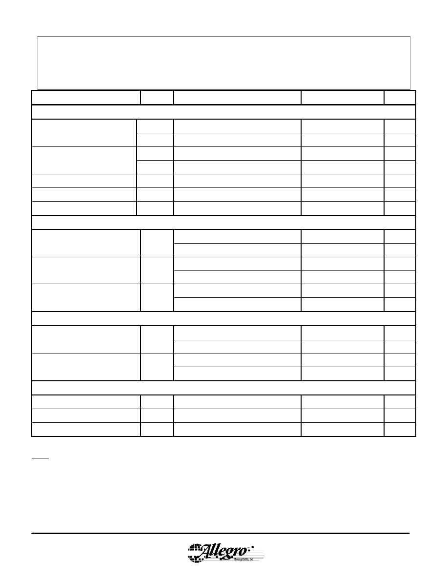
Automotive Power-MOSFET Controller
Characteristics
Symbol
Test Conditions
Min.
Typ.
Max.
Units
Sense Amplifier
Input Bias Current
I
BIAS
CSP=CSN=0 V.
-360
-180
uA
Input Offset Current
I
OS
CSP=CSN=0 V.
-35
35
uA
CSP with respect to gnd.
80
k
Ω
Input Impedance *
R
IN
CSN with respect to gnd.
4
k
Ω
Diff. Input Operating Voltage *
V
ID
V
ID
= CSP – CSN. -1.3V < CSP,N < 4V.
200
mV
Output Offset Voltage
V
OSOUT
CSP=CSN=0V
77
250
450
mV
Output Offset Voltage Drift *
V
OSOUT
CSP=CSN=0V
100
uV/
°
C
Input Common Mode Oper. Range *
V
CM
CSP = CSN
-1.5
4
V
Voltage Gain
A
V
V
ID
= 40
mV to 200
mV
18.6
19.2
19.8
V/V
Low Output Voltage Error
Verr
Vid = 0 to 40
mV, Vout = 19.2*Vid + Vos + Verr
-25
+25
mV
DC Common Mode Gain
A
CM
CSP = CSN = +200
mV
-28
dB
Output Impedance *
R
OUT
V
CSOUT
= 2.0 V
8
Ω
Output Dynamic Range
V
CSOUT
I
CSOUT
= -100
uA at top rail, 100
uA at bottom
rail.
0.075
V
DD
-
.25
V
Output Current, Sink
I
SINK
V
CSOUT
= 2.5 V
20
mA
Output Current, Source
I
SOURCE
V
CSOUT
= 2.5 V
-1
mA
VDD Supply Ripple Gain
PSRG
CSP=CSN=GND. Freq = 0 to 1 MHz
-20
dB
VREG Supply Ripple Gain
PSRG
CSP=CSN=GND. Freq = 0 to 300 kHz
-45
dB
Small Signal 3-dB Bandwidth ( * )
B
10
mv input
1.6
MHz
AC Common
-
Mode Gain
A
cm
Vcm = 250 mV/pp, Freq = 0 to 800 kHz
-26
dB
| Output Slew Rate |
SR
200
mV step input. Meas. 10/90 % points.
10
V/us
3935
Automotive Power-MOSFET Controller
Characteristics
Symbol
Test Conditions
Min.
Typ.
Max.
Units
Fault Logic
VDD Under-voltage
V
UVDD
Decreasing V
DD
3.8
4.3
V
VDD Under-voltage Hysteresis
V
HYSDD
V
UVDD_RECOVERY
= V
UVDD
+ V
HYSDD
100
300
mV
OVSET Operating Voltage Range *
V
OVSET
0
V
DD
V
OVSET Calibrated Voltage Range
V
OVSET
0
2.5
V
OVSET Input Current Range
I
OVSET
-1
+1
uA
VBAT Over-voltage Range
V
OVBAT
0
V < V
OVSET
< 2.5
19.4
40
V
VBAT Over-voltage
V
OVBAT
Increasing V
BAT
, V
OVSET
= 0
v
19.4
22.4
25.4
V
VBAT Over-voltage Hysteresis
V
HYSOVBAT
Percent of V
OVBAT
value set by V
OVSET
9
15
%
VBAT Over-voltage Gain Constant *
K
OVBAT
V
OVBAT
= ( K
OVBAT
∗
V
OVSET
) + V
OVBAT
[0]
12
V/V
VBAT Under-voltage
V
UVBAT
Decreasing V
BAT
5
5.25
5.5
V
VBAT Under-voltage Hysteresis
V
HYSUVBAT
Percent of V
UVBAT
8
12
%
VREG Under-voltage
V
UVREG
Decreasing VREG
9.9
11.1
V
VDSTH Input Range *
V
DSTH
0.5
3
V
VDSTH Input Current
I
DSTH
VDSTH > 0.8
V
40
100
uA
Short-to-Ground Threshold
V
STG
With a High-side driver “on”, as V
SX
decreases,
V
DRAIN
- V
SX
> V
STG
causes a fault.
V
DSTH
-0..3
V
DSTH
+ 0.2
V
Short-to-Battery Threshold
V
STB
With a Low-side driver “on”, as V
SX
increases,
V
SX
- V
LSS
> V
STB
causes a fault.
V
DSTH
-0.3
V
DSTH
+ 0.2
V
V
DRAIN
/Open Bridge Operating
Range
V
DRAIN
7
V < VBAT < 40
V
-0.3
V
BAT
+
2
V
V
DRAIN
/Open Bridge Leakage Curr.
I (V
DRAIN
)
7
V < VBAT < 40
V
.
0
1.0
mA
V
DRAIN
/Open Bridge Threshold Volt.
V
BDGOTH
If V
DRAIN
< V
BDGOTH
then a Bridge fault occurs.
1
3
V
Thermal Shutdown Temp. *
T
J
160
170
180
°C
Thermal Shutdown Hysteresis *
∆
T
J
7
10
13
°C

3935
Automotive Power-MOSFET Controller
Functional Description
Motor Lead Protection.
A fault detection circuit
monitors the voltage across the drain to source of the
external MOSFETs. A fault is asserted “Low” on the output
pin, FAULT\, if the voltage across the drain-to-source of
any MOSFET that is instructed to turn on is greater than the
voltage applied to the V
DSTH
input terminal. When a high-
side switch is turned on, the voltage from pin V
DRAIN
to the
appropriate motor phase output, V
SX
, is examined. If the
motor lead is shorted to ground before the high side is turned
on, the measured voltage will exceed the threshold and the
FAULT\ pin will be go “Low”. Similarly, when a low-side
MOSFET is turned on, the differential voltage between the
motor phase (drain) and the LSS pin (source) is monitored.
The V
DSTH
voltage is set by a resistor divider to V
DD
.
Pin V
DRAIN
is intended to be a Kelvin connection for the
high-side, drain-source monitor circuit. Voltage drops across
the power bus are eliminated by connecting a private PCB
trace from the V
DRAIN
pin to the drain of the MOSFET
bridge. This allows improved accuracy in setting the V
DSTH
threshold voltage. The low-side, drain-source monitor uses
the LSS pin, rather than V
DRAIN
pin, in comparing against the
V
DSTH
voltage.
The A3935 merely reports these motor faults.
Fault Outputs.
Transient faults on any of the fault
outputs are to be expected during switching and will not
disable the gate drive outputs. External circuitry or controller
logic must determine if the faults represent a hazardous
condition.
FAULT
\
.
The FAULT\ terminal will go active “Low” when
any of the following conditions occur:
V
BAT
Overvoltage
V
BAT
Undervoltage
V
REG
Undervoltage
Motor Lead Short-to-Ground
Motor Lead Short-to-Supply (or Battery).
Bridge (or V
DRAIN
) Open
V
DD
Undervoltage
Thermal Shutdown
OVFLT.
Asserts “High” when a V
BAT
Overvoltage fault
occurs and resets after a recovery hysteresis. It has a Hi-Z
state when a thermal shutdown or V
DD
undervoltage
occurs. The voltage at the OVSET pin, V
OVSET
, controls the
V
BAT
overvoltage set point V
OVBAT
, i.e.,
V
OVBAT
= ( K
OVBAT
∗
V
OVSET
) + V
OVBAT
[0],
where K
OVBAT
is the gain and V
OVBAT
[0] is the value of
V
OVBAT
when V
OVSET
is zero. For valid formula, all variables
must be in range and below maximum operating spec.
UVFLT.
Asserts “High” when a V
BAT
undervoltage fault
occurs and resets after a recovery hysteresis. It has a Hi-Z
state when a thermal shutdown or V
DD
undervoltage
occurs. OVFLT and UVFLT are mutually exclusive by
definition.
Current Sensing.
A current sense amplifier is provided
to allow system monitoring of the load current. The
differential amplifier inputs are intended to be Kelvin
connected across a low-value sense resistor or current shunt.
The output voltage is represented by:
V
CSOUT
= ( I
LOAD
∗
A
V
∗
R
SENSE
) + V
OS
Where V
OS
is output voltage calibrated at zero load current
and A
V
= diff amp gain of about 19.
Shutdown.
If a fault occurs because of excessive
junction temperature or undervoltage on V
DD
or V
BAT
, all
gate driver outputs are driven “Low” until the fault condition
is removed. In addition, the boost supply switch and the
VREG are turned “off” until those undervoltages and
junction temperatures recover.
Boost Supply.
The V
BOOST
voltage is controlled by an
inner current-control loop, and by an outer voltage-feedback
loop. The current-control loop turns “off” the boost switch
for 5 us whenever the voltage across the boost current-sense
resistor exceeds 500 mV. A diode reverse-recovery current
flows through the sense resistor whenever the boost switch
turns “on” that could turn it “off”, again, if not for the
“blanking time” circuit. Adjustment of this external sense
resistor determines the maximum current in the inductor.
Whenever V
BOOST
exceeds the predefined threshold,
nominally 16 V, the boost switch is inhibited.
3935
Automotive Power-MOSFET Controller
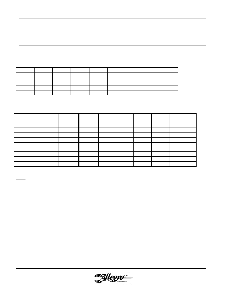
Input Logic.
Enable
(x)LO
(x)HI
GL(x)
GH(x)
Mode of Operation
0
X
X
0
0
All gate
-
drive outputs Low
1
0
0
0
0
All gate drive outputs Low
1
0
1
0
1
High Side On
1
1
0
1
0
Low Side On
1
1
1
0
0
XOR feature prevents shoot-through.
Fault Responses.
FAULT MODE
ENABLE
FA
ULT\ OVFLT UVFLT BOOST
REG.
VREG
REG.
GH
X
GL
X
No Fault
X
1
0
0
ON
ON
-
-
Short-to-Battery
1*
0
0
0
ON
ON
-
-
Short-to-Ground
1*
0
0
0
ON
ON
-
-
V
REG
Undervoltage
X
0
0
0
ON
ON
-
-
V
DD
Undervoltage or
Thermal Shutdown !
X
0
Z
Z
OFF
OFF
0
0
Bridge (V
DRAIN
) Fault
1*
0
0
0
ON
ON
-
-
V
BAT
Overvoltage
X
0
1
0
OFF*
ON
-
-
V
BAT
Undervoltage !
X
0
0
1
O FF
OFF
0
0
Notes:
OFF* = Off, only because V
BOOST
~ V
BAT
is above the voltage threshold of the regulator’s voltage control loop.
x = “little x ”indicates A, B, or C phase.
X = “Capital X “ indicates a “don’t care”.
- = Depends on (x)LO, (x)HI inputs and ENABLE.
Z = Tri-stated output.
1* = Short-to-Battery can only be detected when the corresponding GL
X
= 1. Similarly, Short-to-Ground can only be
detected when the corresponding GH
X
= 1. Bridge Fault appears as a Short-to-Ground Fault on all motor phases.
These faults are not detected when ENABLE = 0
! = These Faults are not only reported but action is taken by the internal logic to protect the 3935 and the system.
3935
Automotive Power-MOSFET Controller
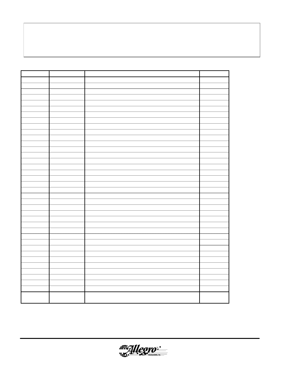
Terminal List
LQ pin #
Pin Name
Pin Description
ED pin #
1
CSP
Current
-
sense input, positive-side
31
2
VDSTH
DC Input, Drain-to-Source Monitor Threshold Voltage
32
3
LSS
Low-Side, Gate Drive Source returns
33
4
GLC
Low-Side C Gate Drive Output
36
5
SC
Motor Phase C Input
37
6
GHC
High-Side C Gate Drive Output
38
7
CC
Bootstrap C Cap
39
8
GLB
Low
-
Side B Gate Drive Output
40
9
SB
Motor Phase B Input
41
10
GHB
High-Side B Gate Drive Output
42
11
CB
Bootstrap B Cap
43
12
GLA
Low-Side A Gate Drive Output
44
13
SA
Motor Phase A Input
3
14
GHA
High-Side A Gate Drive Output
4
15
CA
Bootstrap A Cap
5
16
VREG
Gate Drive Supply, Positive
6
17
VDRAIN
Kelvin Connection to MOSFET
H
igh-
S
ide
D
rain
7
18
VBOOST
Boost Supply Output
8
19
BOOSTS
Boost Switch, Source
9
20
BOOSTD
Boost Switch, Drain
10
21
GND
G
round
, DC Supply
R
eturns, Negative
12
22
VBAT
Battery Supply Connection, Positive
13
23
UVFLT
VBAT Undervoltage Fault
14
24
OVFLT
VBAT Overvoltage Fault
15
25
FAULT\
Fault Output, Primary
16
26
ALO
Gate Control Signal, A, Low-
S
ide
17
27
AHI
Gate Control Signal, A, High-
S
ide
18
28
BHI
Gate Control Signal, B, High-
S
ide
19
29
BLO
Gate Control Signal, B, Low-
S
ide
20
30
CLO
Gate Control Signal, C, Low-
S
ide
21
31
CHI
Gate Control Signal, C, High-
S
ide
24
32
ENABLE
Gate Output Enable
25
33
OVSET
DC
I
nput, Overvoltage Threshold Setting for VBAT
26
-
TP
Test Point for manufacturing test use, only.
27
34
CSOUT
Current
-S
ense
A
mplifier
O
utput
28
35
VDD
Logic Supply, Positive
29
36
CSN
Current
-S
ense
I
nput,
N
egative-
S
ide
30
-
GND
GROUND, DC Supply
R
eturns, Negative. Heat
P
ath,
D
ie
A
ttach,
C
onnected to
C
hip GND at
Terminal
12.
1,2,11,12,22,
23,34,35
Wyszukiwarka
Podobne podstrony:
3935
3935
3935
3935
3935
3935
3935
3935
3935
200412 3935
3935
3935
3935
org lett 3 3935 salvinorin c
więcej podobnych podstron