VISHAY
SFH615A / SFH6156
Document Number 83671
Rev. 1.5, 19-Apr-04
Vishay Semiconductors
www.vishay.com
1
1
2
4
3
E
C
A
C
17448
1
1
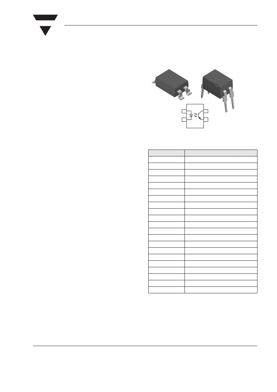
Optocoupler, High Reliability, 5300 V
RMS
Features
• Excellent CTR Linearity Depending on
Forward Current
• Isolation Test Voltage, 5300 V
RMS
• Fast Switching Times
• Low CTR Degradation
• Low Coupling Capacitance
Agency Approvals
• UL - File No. E52744 System Code H or J
• DIN EN 60747-5-2(VDE0884)
DIN EN 60747-5-5 pending
Available with Option 1
Applications
Switchmode power supply
Telecom
Battery powered equipment
Description
The SFH615A (DIP) and SFH6156 (SMD) feature a
variety of transfer ratios, low coupling capacitance
and high isolation voltage. These couplers have a
GaAs infrared diode emitter, which is optically cou-
pled to a silicon planar phototransistor detector, and
is incorporated in a plastic DIP-4 or SMD package.
The coupling devices are designed for signal trans-
mission between two electrically separated circuits.
The couplers are end-stackable with 2.54 mm lead
spacing.
Creepage and clearance distances of > 8.0 mm are
achieved with option 6. This version complies with
IEC 60950 (DIN VDE 0805) for reinforced insulation
up to an operation voltage of 400 V
RMS
or DC.
Specifications subject to change.
Order Information
For additional information on the available options refer to
Option Information.
See TAPE AND REEL Section for 4-pin optocouplers T0 with 90 °
rotation.
Part
Remarks
SFH615A-1
CTR 40 - 80 %, DIP-4
SFH615A-2
CTR 63 - 125 %, DIP-4
SFH615A-3
CTR 100 - 200 %, DIP-4
SFH615A-4
CTR 160 - 320 %, DIP-4
SFH6156-1
CTR 40 - 80 %, SMD-4
SFH6156-2
CTR 63 - 125 %, SMD-4
SFH6156-3
CTR 100 - 200 %, SMD-4
SFH6156-4
CTR 160 - 320 %, SMD-4
SFH615A-1-X006
CTR 40 - 80 %, DIP-4 400 mil (option 6)
SFH615A-1-X007
CTR 40 - 80 %, SMD-4 (option 7)
SFH615A-2-X006
CTR 63 - 125 %, DIP-4 400 mil (option 6)
SFH615A-2-X007
CTR 63 - 125 %, SMD-4 (option 7)
SFH615A-2-X009
CTR 63 - 125 %, SMD-4 (option 9)
SFH615A-3-X006
CTR 100 - 200 %, DIP-4 400 mil (option 6)
SFH615A-3-X007
CTR 100 - 200 %, SMD-4 (option 7)
SFH615A-3-X008
CTR 100 - 200 %, SMD-4 (option 8)
SFH615A-3-X009
CTR 100 - 200 %, SMD-4 (option 9)
SFH615A-4-X006
CTR 160 - 320 %, DIP-4 400 mil (option 6)
SFH615A-4-X007
CTR 160 - 320 %, SMD-4 (option 7)
SFH615A-4-X008
CTR 160 - 320 %, SMD-4 (option 7)
SFH615A-4-X009
CTR 160 - 320 %, SMD-4 (option 7)
www.vishay.com
2
Document Number 83671
Rev. 1.5, 19-Apr-04
VISHAY
SFH615A / SFH6156
Vishay Semiconductors
Absolute Maximum Ratings
T
amb
= 25 °C, unless otherwise specified
Stresses in excess of the absolute Maximum Ratings can cause permanent damage to the device. Functional operation of the device is
not implied at these or any other conditions in excess of those given in the operational sections of this document. Exposure to absolute
Maximum Rating for extended periods of the time can adversely affect reliability.
Input
Output
Coupler
Parameter
Test condition
Symbol
Value
Unit
Reverse voltage
V
R
6.0
V
DC Forward current
I
F
60
mA
Surge forward current
t
p
≤ 10 µs
I
FSM
2.5
A
Power dissipation
P
diss
100
mW
Parameter
Test condition
Symbol
Value
Unit
Collector-emitter voltage
V
CE
70
V
Emitter-collector voltage
V
CEO
7.0
V
Collector current
I
C
50
mA
t
p
≤ 1.0 ms
I
C
100
mA
Power dissipation
P
diss
150
mW
Parameter
Test condition
Symbol
Value
Unit
Isolation test voltage (between
emitter and detector, refered to
climate DIN 40046, part 2,
Nov. 74
t = 1.0 s
V
ISO
5300
V
RMS
Creepage
≥ 7.0
mm
Clearance
≥ 7.0
mm
Insulation thickness between
emitter and detector
≥ 0.4
mm
Comparative tracking index per
DIN IEC 112/VDE 0303, part 1
≥ 175
Isolation resistance
V
IO
= 500 V, T
amb
= 25 °C
R
IO
≥ 10
12
Ω
V
IO
= 500 V, T
amb
= 100 °C
R
IO
≥ 10
11
Ω
Storage temperature range
T
stg
- 55 to + 150
°C
Ambient temperature range
T
amb
- 55 to + 100
°C
Junction temperature
T
j
100
°C
Soldering temperature
max. 10 s, Dip soldering
distance to seating plane
≥ 1.5 mm
T
sld
260
°C
VISHAY
SFH615A / SFH6156
Document Number 83671
Rev. 1.5, 19-Apr-04
Vishay Semiconductors
www.vishay.com
3
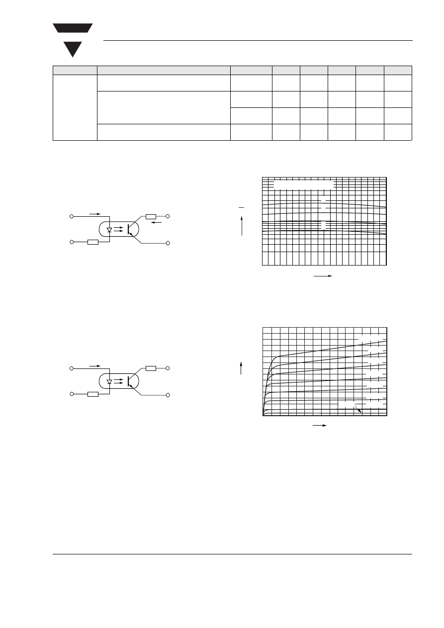
Electrical Characteristics
T
amb
= 25 °C, unless otherwise specified
Minimum and maximum values are testing requirements. Typical values are characteristics of the device and are the result of engineering
evaluation. Typical values are for information only and are not part of the testing requirements.
Input
Output
Coupler
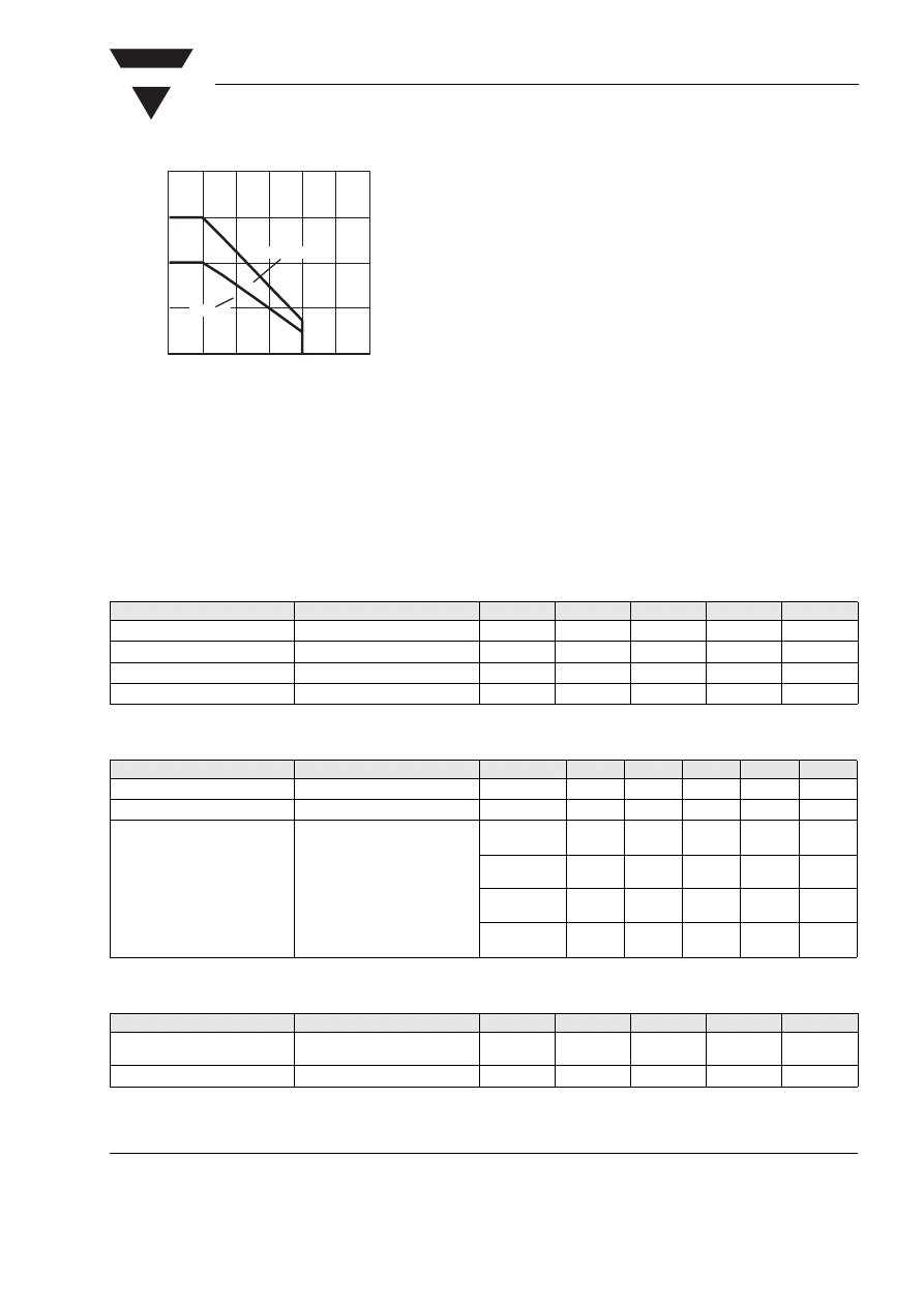
Fig. 1 Permissible Power Dissipation vs. Ambient Temperature
0
50
100
150
200
0
25
50
75
100
125
150
18483
P
–Power Dissipation (mW)
tot
Phototransistor
Diode
T
amb
– Ambient Temperature (
qC )
Parameter
Test condition
Symbol
Min
Typ.
Max
Unit
Forward voltage
I
F
= 60mA
V
F
1.25
1.65
V
Reverse current
V
R
= 6.0 V
I
R
0.01
10
µA
Capacitance
V
R
= 0 V, f = 1.0 MHz
C
O
13
pF
Thermal resistance
R
thja
750
K/W
Parameter
Test condition
Part
Symbol
Min
Typ.
Max
Unit
Collector-emitter capacitance
V
CE
= 5.0 V, f = 1.0 MHz
C
CE
5.2
pF
Thermal resistance
R
thja
500
K/W
Collector-emitter leakage
current
V
CE
= 10 V
SFH615A-1
SFH6156-1
I
CEO
2.0
50
nA
SFH615A-2
SFH6156-2
I
CEO
2.0
50
nA
SFH615A-3
SFH6156-3
I
CEO
5.0
100
nA
SFH615A-4
SFH6156-4
I
CEO
5.0
100
nA
Parameter
Test condition
Symbol
Min
Typ.
Max
Unit
Collector-emitter saturation
voltage
I
F
= 10 mA, I
C
= 2.5 mA
V
CEsat
0.25
0.4
V
Coupling capacitance
C
C
0.4
pF
www.vishay.com
4
Document Number 83671
Rev. 1.5, 19-Apr-04
VISHAY
SFH615A / SFH6156
Vishay Semiconductors
Current Transfer Ratio
Switching Characteristics
Switching Non-saturated
Switching Saturated
Parameter
Test condition
Part
Symbol
Min
Typ.
Max
Unit
I
C
/I
F
I
F
= 10 mA, V
CE
= 5.0 V
SFH615A-1
SFH6156-1
CTR
40
80
%
SFH615A-2
SFH6156-2
CTR
63
125
%
SFH615A-3
SFH6156-3
CTR
100
200
%
SFH615A-4
SFH6156-4
CTR
160
320
%
I
F
= 1.0 mA, V
CE
= 5.0 V
SFH615A-1
SFH6156-1
CTR
13
30
%
SFH615A-2
SFH6156-2
CTR
22
45
%
SFH615A-3
SFH6156-3
CTR
34
70
%
SFH615A-4
SFH6156-4
CTR
56
90
%
Parameter
Test condition
Symbol
Min
Typ.
Max
Unit
Rise Time
I
F
= 10 mA, V
CC
= 5.0 V, T
A
= 25 °C, R
L
= 75
Ω
t
r
2.0
µs
Fall Time
I
F
= 10 mA, V
CC
= 5.0 V, T
A
= 25 °C, R
L
= 75
Ω
t
f
2.0
µs
Turn-on time
I
F
= 10 mA, V
CC
= 5.0 V, T
A
= 25 °C, R
L
= 75
Ω
t
on
3.0
µs
Turn-off time
I
F
= 10 mA, V
CC
= 5.0 V, T
A
= 25 °C, R
L
= 75
Ω
t
off
2.3
µs
Cut-off
frequency
I
F
= 10 mA, V
CC
= 5.0 V, T
A
= 25 °C, R
L
= 75
Ω
f
ctr
250
kHz
Parameter
Test condition
Part
Symbol
Min
Typ.
Max
Unit
Rise time
V
CC
= 5.0 V, T
A
= 25 °C, R
L
= 1 k
Ω, I
F
= 20 mA
SFH615A-1
SFH6156-1
t
r
2.0
µs
V
CC
= 5.0 V, T
A
= 25 °C, R
L
= 1 k
Ω, I
F
= 10 mA
SFH615A-2
SFH6156-2
t
r
3.0
µs
SFH615A-3
SFH6156-3
t
r
3.0
µs
V
CC
= 5.0 V, T
A
= 25 °C, R
L
= 1 k
Ω, I
F
= 5.0 mA
SFH615A-4
SFH6156-4
t
r
4.6
µs
Fall time
V
CC
= 5.0 V, T
A
= 25 °C, R
L
= 1 k
Ω, I
F
= 20 mA
SFH615A-1
SFH6156-1
t
f
11
µs
V
CC
= 5.0 V, T
A
= 25 °C, R
L
= 1 k
Ω, I
F
= 10 mA
SFH615A-2
SFH6156-2
t
f
14
µs
SFH615A-3
SFH6156-3
t
f
14
µs
V
CC
= 5.0 V, T
A
= 25 °C, R
L
= 1 k
Ω, I
F
= 5.0 mA
SFH615A-4
SFH6156-4
t
f
15
µs
Turn-on time
V
CC
= 5.0 V, T
A
= 25 °C, R
L
= 1 k
Ω, I
F
= 20 mA
SFH615A-1
SFH6156-1
t
on
3.0
µs
V
CC
= 5.0 V, T
A
= 25 °C, R
L
= 1 k
Ω, I
F
= 10 mA
SFH615A-2
SFH6156-2
t
on
4.2
µs
SFH615A-3
SFH6156-3
t
on
4.2
µs
V
CC
= 5.0 V, T
A
= 25 °C, R
L
= 1 k
Ω, I
F
= 5.0 mA
SFH615A-4
SFH6156-4
t
on
6.0
µs
VISHAY
SFH615A / SFH6156
Document Number 83671
Rev. 1.5, 19-Apr-04
Vishay Semiconductors
www.vishay.com
5
Typical Characteristics
(T
amb
= 25
°C unless otherwise specified)
Turn-off time
V
CC
= 5.0 V, T
A
= 25 °C, R
L
= 1 k
Ω, I
F
= 20 mA
SFH615A-1
SFH6156-1
t
off
18
µs
V
CC
= 5.0 V, T
A
= 25 °C, R
L
= 1 k
Ω, I
F
= 10 mA
SFH615A-2
SFH6156-2
t
off
23
µs
SFH615A-3
SFH6156-3
t
off
23
µs
V
CC
= 5.0 V, T
A
= 25 °C, R
L
= 1 k
Ω, I
F
= 5.0 mA
SFH615A-4
SFH6156-4
t
off
25
µs
Parameter
Test condition
Part
Symbol
Min
Typ.
Max
Unit
Fig. 2 Linear Operation ( without Saturation)
Fig. 3 Switching Operation (with Saturation)
isfh615a_01
R
L
= 75 Ω
V
CC
= 5 V
I
C
47 Ω
I
F
isfh615a_02
1 Ω
V
CC
= 5 V
47 Ω
I
F
Fig. 4 Current Transfer Ratio (typical) vs. Temperature
Fig. 5 Output Characteristics (typ.) Collector Current vs.
Collector-Emitter Voltage
isfh615a_01
–25
0
25
50
°C
75
10
3
10
2
10
1
5
5
%
IC
IF
TA
4
3
2
1
IF = 10 mA, VCE = 5.0 V
isfh615a_04
30
20
10
0
0
5
10
V
15
IF=14 mA
2.0 mA
4.0 mA
6.0 mA
8.0 mA
10 mA
12 mA
1.0 mA
mA
IC
VCE
www.vishay.com
6
Document Number 83671
Rev. 1.5, 19-Apr-04
VISHAY
SFH615A / SFH6156
Vishay Semiconductors
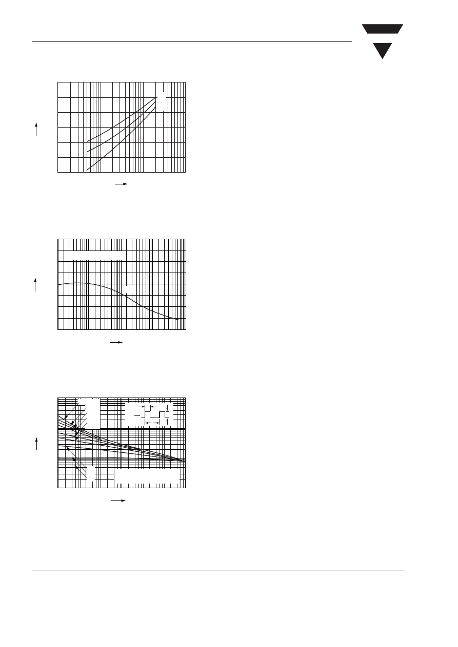
Fig. 6 Diode Forward Voltage (typ.) vs. Forward Current
Fig. 7 Transistor Capacitance (typ.) vs. Collector-Emitter Voltage
Fig. 8 Permissible Pulse Handling Capability Forward Current vs.
Pulse Width
isfh615a_05
VF
IF
25°
50°
75°
1.2
1.1
1.0
0.9
10
–1
10
0
10
1
mA
10
2
V
isfh615a_06
20
15
10
5
0
pF
C
Ve
10
–2
10
–1
10
–0
10
1
V
10
2
C CE
f = 1.0 MHz
isfh615a_07
IF
tp
10
–5
10
–4
10
–3
10
–2
10
–1
10
0
s 10
1
10
4
10
3
10
2
10
1
5
5
5
mA
D=
t
p
T
t
p
I
F
T
D=0
0.005
0.01
0.02
0.05
0.1
0.2
0.5
DC
Pulse cycle D = parameter
VISHAY
SFH615A / SFH6156
Document Number 83671
Rev. 1.5, 19-Apr-04
Vishay Semiconductors
www.vishay.com
7
Package Dimensions in Inches (mm)
Package Dimensions in Inches (mm)
i178027
.255 (6.48)
.268 (6.81)
1
2
4
3
.179 (4.55)
.190 (4.83)
pin one ID
.030 (.76)
.045 (1.14)
4°
typ.
.100 (2.54)
.130 (3.30)
.150 (3.81)
.020 (.508 )
.035 (.89)
10°
3°–9°
.018 (.46)
.022 (.56)
.008 (.20)
.012 (.30)
.031 (.79) typ.
.050 (1.27) typ.
.300 (7.62) typ.
.110 (2.79)
.130 (3.30)
.230 (5.84)
.250 (6.35)
.050 (1.27)
ISO Method A
i178029
.255 (6.48)
.268 (6.81)
3
4
.179 (4.55)
.190 (4.83)
pin one ID
.030 (.76)
.045 (1.14)
4° typ.
1.00 (2.54)
typ.
.130 (3.30)
.150 (3.81)
.0098 (.249)
.035 (.102)
.020 (.508)
.040 (1.02)
.031 (.79)
typ.
.050 (1.27)
typ.
.010 (.25)
typ.
10°
3°–7°
.375 (9.52)
.305 (10.03)
.296 (7.52)
.312 (7.90)
.315 (8.00)
min.
Lead
coplanarity
.004 max.
SMD
ISO Method A
.100 (2.54)
R .010 (.25)
.070 (1.78)
.030 (.76)
.315 (8.00) min
.060 (1.52)
.435 (11.05)
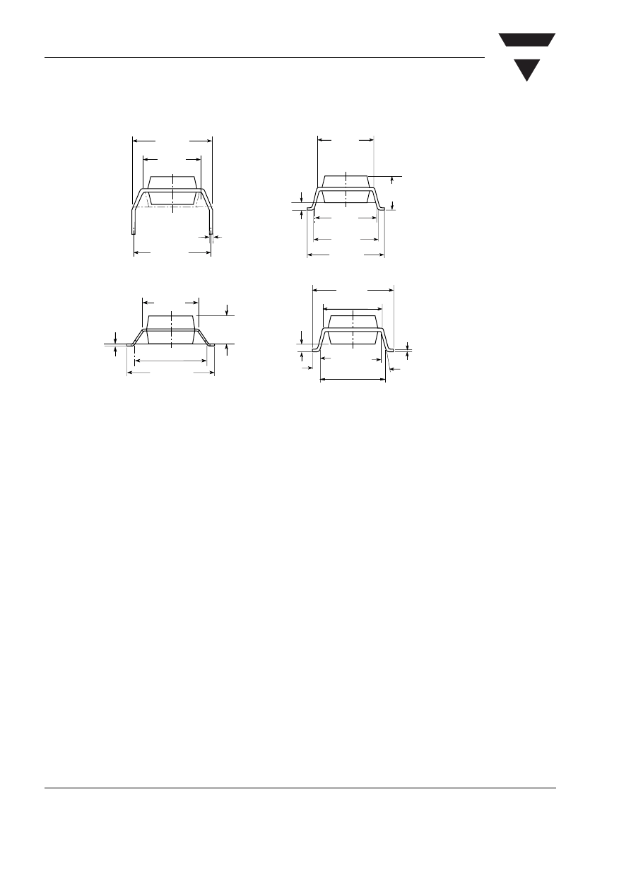
www.vishay.com
8
Document Number 83671
Rev. 1.5, 19-Apr-04
VISHAY
SFH615A / SFH6156
Vishay Semiconductors
min.
.315 (8.00)
.300 (7.62)
TYP.
.150 (3.81)
.130 (3.30)
.472 (12.00)
MAX.
.365 (9.27)
MIN.
.020 (0.50)
.000 (0.00)
Option 8
.014 (0.35)
.010 (0.25)
.400 (10.16)
.430 (10.92)
.307 (7.8)
.291 (7.4)
.407 (10.36)
.391 (9.96)
Option 6
.315 (8.0)
MIN.
.300 (7.62)
TYP.
.180 (4.6)
.160 (4.1)
.331 (8.4)
MIN.
.406 (10.3)
MAX.
.028 (0.7)
MIN.
Option 7
.020 (.51)
.040 (1.02)
.300 (7.62)ref.
.375 (9.53)
.395 (10.03)
.012 (.30) typ.
0040 (.102)
0098 (.249)
15° max.
Option 9
18486

VISHAY
SFH615A / SFH6156
Document Number 83671
Rev. 1.5, 19-Apr-04
Vishay Semiconductors
www.vishay.com
9
Ozone Depleting Substances Policy Statement
It is the policy of Vishay Semiconductor GmbH to
1. Meet all present and future national and international statutory requirements.
2. Regularly and continuously improve the performance of our products, processes, distribution and
operatingsystems with respect to their impact on the health and safety of our employees and the public, as
well as their impact on the environment.
It is particular concern to control or eliminate releases of those substances into the atmosphere which are
known as ozone depleting substances (ODSs).
The Montreal Protocol (1987) and its London Amendments (1990) intend to severely restrict the use of ODSs
and forbid their use within the next ten years. Various national and international initiatives are pressing for an
earlier ban on these substances.
Vishay Semiconductor GmbH has been able to use its policy of continuous improvements to eliminate the
use of ODSs listed in the following documents.
1. Annex A, B and list of transitional substances of the Montreal Protocol and the London Amendments
respectively
2. Class I and II ozone depleting substances in the Clean Air Act Amendments of 1990 by the Environmental
Protection Agency (EPA) in the USA
3. Council Decision 88/540/EEC and 91/690/EEC Annex A, B and C (transitional substances) respectively.
Vishay Semiconductor GmbH can certify that our semiconductors are not manufactured with ozone depleting
substances and do not contain such substances.
We reserve the right to make changes to improve technical design
and may do so without further notice.
Parameters can vary in different applications. All operating parameters must be validated for each
customer application by the customer. Should the buyer use Vishay Semiconductors products for any
unintended or unauthorized application, the buyer shall indemnify Vishay Semiconductors against all
claims, costs, damages, and expenses, arising out of, directly or indirectly, any claim of personal
damage, injury or death associated with such unintended or unauthorized use.
Vishay Semiconductor GmbH, P.O.B. 3535, D-74025 Heilbronn, Germany
Telephone: 49 (0)7131 67 2831, Fax number: 49 (0)7131 67 2423
Document Outline
Wyszukiwarka
Podobne podstrony:
BYV27 50 BYV27 200 (Vishay)
BF970 Vishay elenota pl
BF966S (Vishay)
więcej podobnych podstron