4
5
6
7
8
9
10
19
20
21
22
23
24
25
LOAD
SUPPLY
BB
V
OUT
2
OUT
7
OUT
8
Dwg. PP-029-7
OUT
19
OUT
18
OUT
13
12
13
14
27
28
17
18
SERIAL
DATA OUT
BLANKING
LOGIC
SUPPLY
STROBE
GROUND
CLOCK
CLK
ST
BLNK
OUT
9
OUT
10
OUT
12
OUT
11
11
LATCHES
REGISTER
REGISTER
LATCHES
2
3
26
27
28
SERIAL
DATA IN
OUT
6
OUT
1
OUT
4
OUT
3
OUT
20
1
15
16
OUT
5
OUT
17
OUT
16
OUT
15
OUT
14
DD
V
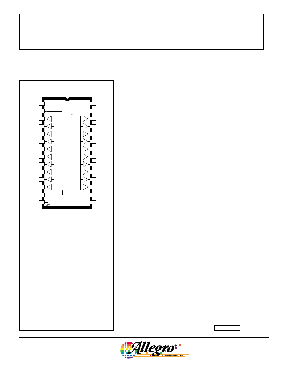
DABiC-IV, 20-BIT SERIAL-INPUT,
LATCHED SOURCE DRIVER
A6812xA
(DIP)
Data Sheet
26182.126B
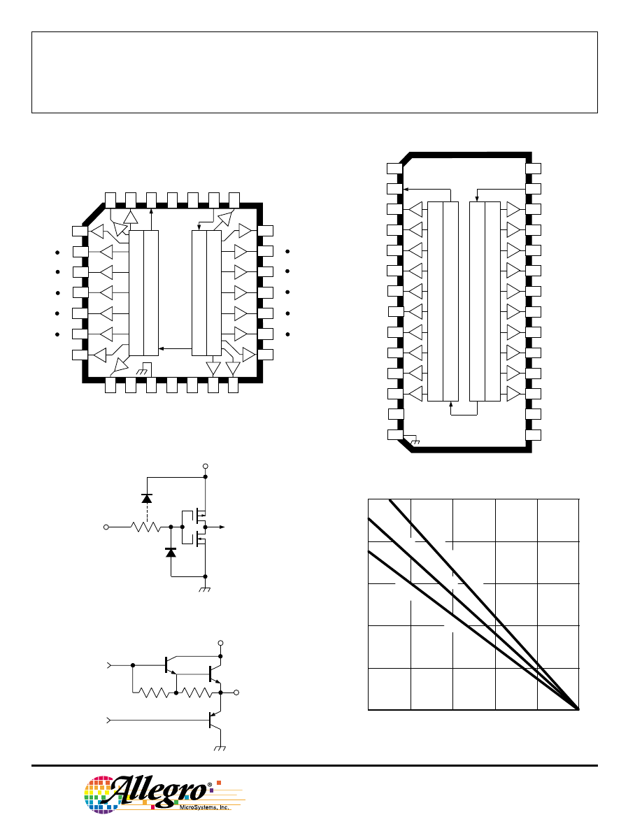
ABSOLUTE MAXIMUM RATINGS
at T
A
= 25
°
C
Logic Supply Voltage, V
DD
................... 7.0 V
Driver Supply Voltage, V
BB
................... 60 V
Continuous Output Current Range,
I
OUT
......................... -40 mA to +15 mA
Input Voltage Range,
V
IN
....................... -0.3 V to V
DD
+ 0.3 V
Package Power Dissipation,
P
D
........................................ See Graph
Operating Temperature Range, T
A
(Suffix ‘E–’) .................. -40
°
C to +85
°
C
(Suffix ‘K–’) ................ -40
°
C to +125
°
C
(Suffix ‘S–’) .................. -20
°
C to +85
°
C
Storage Temperature Range,
T
S
............................... -55
°
C to +125
°
C
Caution: These CMOS devices have input static
protection (Class 2) but are still susceptible to
damage if exposed to extremely high static
electrical charges.
The A6812– devices combine a 20-bit CMOS shift register,
accompanying data latches and control circuitry with bipolar sourcing
outputs and pnp active pull downs. Designed primarily to drive
vacuum-fluorescent displays, the 60 V and -40 mA output ratings also
allow these devices to be used in many other peripheral power driver
applications. The A6812– features an increased data input rate (com-
pared with the older UCN/UCQ5812-F) and a controlled output slew
rate.
The CMOS shift register and latches allow direct interfacing with
microprocessor-based systems. With a 3.3 V or 5 V logic supply, they
will operate to at least 10 MHz.
A CMOS serial data output permits cascade connections in applica-
tions requiring additional drive lines. Similar devices are available as
the A6809– and A6810– (10 bits), A6811– (12 bits), and A6818– (32
bits).
The A6812– output source drivers are npn Darlingtons, capable of
sourcing up to 40 mA. The controlled output slew rate reduces electro-
magnetic noise, which is an important consideration in systems that
include telecommunications and/or microprocessors and to meet
government emissions regulations. For inter-digit blanking, all output
drivers can be disabled and all sink drivers turned on with a BLANK-
ING input high. The pnp active pull-downs will sink at least 2.5 mA.
Three temperature ranges are available for optimum performance
in commercial (suffix S-), industrial (suffix E-), or automotive (suffix
K-) applications. Package styles are provided for through-hole DIP
(suffix -A), surface-mount SOIC (suffix -LW), or minimum-area
surface-mount PLCC (suffix -EP). Copper lead frames, low logic-
power dissipation, and low output-saturation voltages allow these
drivers to source 25 mA from all outputs continuously to more than
+43
°
C (suffix -LW), +61
°
C (suffix -EP), or +77
°
C (suffix -A).
FEATURES
■
Controlled Output Slew Rate
■
High-Speed Data Storage
■
60 V Minimum
Output Breakdown
■
High Data Input Rate
■
PNP Active Pull-Downs
Complete part number includes a suffix to identify operating
temperature range (E-, K-, or S-) and package type (-A, -EP, or -LW).
Always order by complete part number, e.g., A6812SLW .
6812
■
Low Output-Saturation Voltages
■
Low-Power CMOS Logic
and Latches
■
Improved Replacements
for TL5812–, UCN5812–,
and UCQ5812–
6812
20-BIT SERIAL-INPUT,
LATCHED SOURCE DRIVER
115 Northeast Cutoff, Box 15036
Worcester, Massachusetts 01615-0036 (508) 853-5000
A6812xLW
(SOIC)
4
5
6
7
8
9
10
19
20
21
22
23
24
25
LOAD
SUPPLY
BB
V
OUT
2
OUT
7
OUT
8
Dwg. PP-029-8
OUT
19
OUT
18
OUT
13
12
13
14
27
28
17
18
SERIAL
DATA OUT
BLANKING
LOGIC
SUPPLY
STROBE
GROUND
CLOCK
CLK
ST
BLNK
OUT
9
OUT
10
OUT
12
OUT
11
11
LATCHES
REGISTER
REGISTER
LATCHES
2
3
26
27
28
SERIAL
DATA IN
OUT
6
OUT
1
OUT
4
OUT
3
OUT
20
1
15
16
OUT
5
OUT
17
OUT
16
OUT
15
OUT
14
DD
V
TYPICAL INPUT CIRCUIT
Dwg. EP-010-5
IN
V
DD
2
3
4
5
6
7
8
9
12
13
14
15
16
28
1
V
DD
Dwg. PP-059-1
OUT
10
OUT
20
OUT
11
OUT
19
REGISTER
LATCHES
V
BB
CLOCK
ST
CLK
26
27
22
23
24
25
SERIAL
DATA OUT
LOAD
SUPPLY
SERIAL
DATA IN
10
11
STROBE
GROUND
LOGIC
SUPPLY
19
20
21
BLANKING
17
18
OUT
9
OUT
1
OUT
2
OUT
8
OUT
18
OUT
12
LATCHES
REGISTER
50
75
100
125
150
2.5
0.5
0
ALLOWABLE PACKAGE POWER DISSIPATION IN WATTS
AMBIENT TEMPERATURE IN
°°°°
C
2.0
1.5
1.0
25
Dwg. GP-024-2
SUFFIX 'LW', R = 66
°
C/W
θ
JA
SUFFIX 'EP', R = 55
°
C/W
θ
JA
SUFFIX 'A', R = 45
°
C/W
θ
JA
V
BB
Dwg. EP-021-19
OUT
N
TYPICAL OUTPUT DRIVER
Copyright © 2000, 2002 Allegro MicroSystems, Inc.
A6812xEP
(PLCC)
6812
20-BIT SERIAL-INPUT,
LATCHED SOURCE DRIVER
www.allegromicro.com
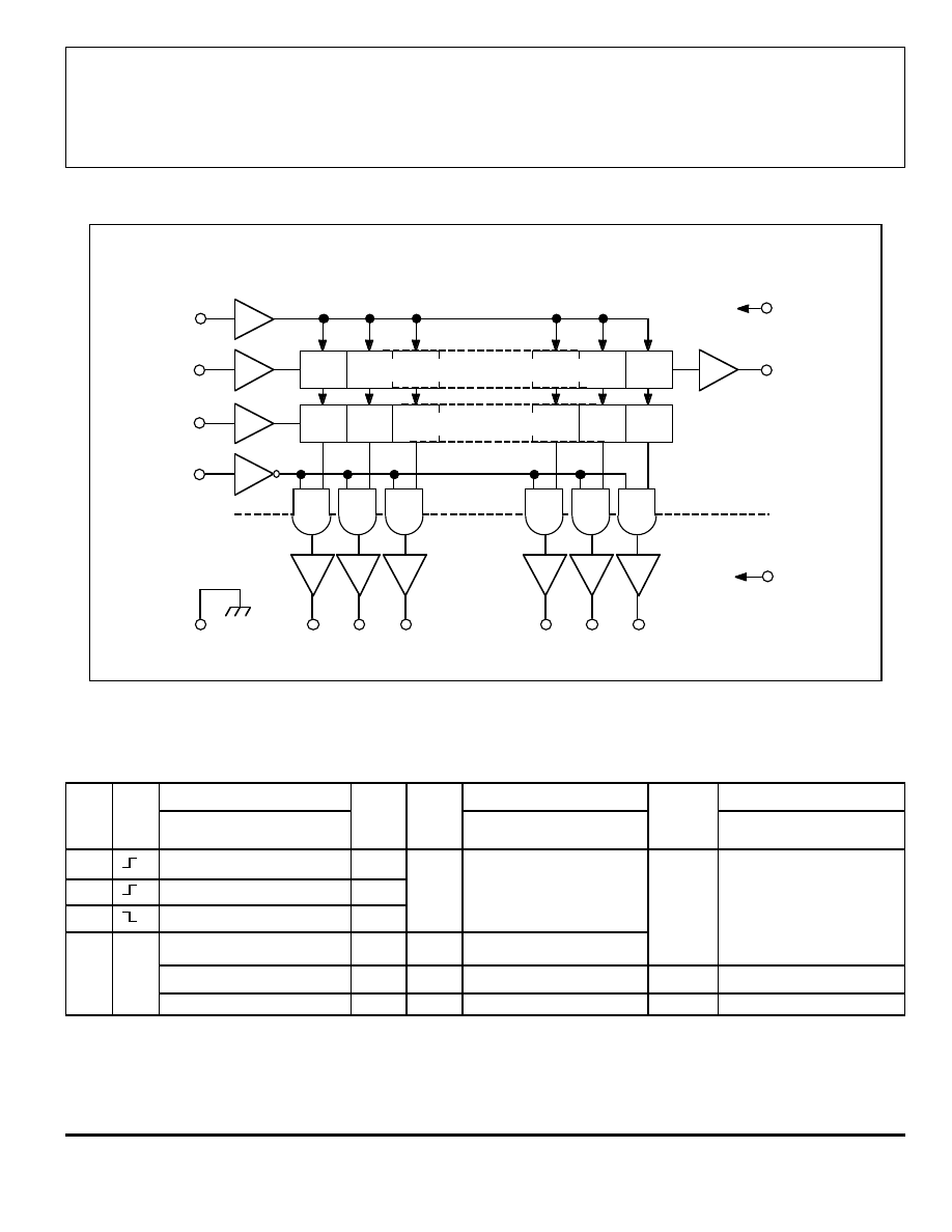
FUNCTIONAL BLOCK DIAGRAM
TRUTH TABLE
Serial
Shift Register Contents
Serial
Latch Contents
Output Contents
Data
Clock
Data
Strobe
Input
Input I
1
I
2
I
3
...
I
N-1
I
N
Output
Input
I
1
I
2
I
3
...
I
N-1
I
N
Blanklng
I
1
I
2
I
3
... I
N-1
I
N
H
H
R
1
R
2
...
R
N-2
R
N-1
R
N-1
L
L
R
1
R
2
...
R
N-2
R
N-1
R
N-1
X
R
1
R
2
R
3
...
R
N-1
R
N
R
N
X
X
X
...
X
X
X
L
R
1
R
2
R
3
...
R
N-1
R
N
P
1
P
2
P
3
...
P
N-1
P
N
P
N
H
P
1
P
2
P
3
...
P
N-1
P
N
L
P
1
P
2
P
3
... P
N-1
P
N
X
X
X
...
X
X
H
L
L
L
... L
L
L = Low Logic Level H = High Logic Level X = Irrelevant P = Present State R = Previous State
MOS
BIPOLAR
OUT
1
OUT
2
GROUND
Dwg. FP-013-1
OUT
3
OUT
N
CLOCK
SERIAL
DATA IN
STROBE
BLANKING
SERIAL
DATA OUT
SERIAL-PARALLEL SHIFT REGISTER
LATCHES
V
DD
V
BB
LOGIC
SUPPLY
LOAD
SUPPLY
6812
20-BIT SERIAL-INPUT,
LATCHED SOURCE DRIVER
115 Northeast Cutoff, Box 15036
Worcester, Massachusetts 01615-0036 (508) 853-5000
ELECTRICAL CHARACTERISTICS at T
A
= +25
°
C (A6812S-) or over operating temperature
range (A6812E- or A6812K-), V
BB
= 60 V unless otherwise noted.
Limits @ V
DD
= 3.3 V Limits @ V
DD
= 5 V
Characteristic
Symbol
Test Conditions
Mln.
Typ.
Max.
Min.
Typ.
Max.
Units
Output Leakage Current
I
CEX
V
OUT
= 0 V
—
<-0.1
-15
—
<-0.1
-15
µ
A
Output Voltage
V
OUT(1)
I
OUT
= -25 mA
57.5
58.3
—
57.5
58.3
—
V
V
OUT(0)
I
OUT
= 1 mA
—
1.0
1.5
—
1.0
1.5
V
Output Pull-Down Current
I
OUT(0)
V
OUT
= 5 V to V
BB
2.5
5.0
—
2.5
5.0
—
mA
Input Voltage
V
IN(1)
2.2
—
—
3.3
—
—
V
V
IN(0)
—
—
1.1
—
—
1.7
V
Input Current
I
IN(1)
V
IN
= V
DD
—
<0.01
1.0
—
<0.01
1.0
µ
A
I
IN(0)
V
IN
= 0 V
—
<-0.01
-1.0
—
<-0.01
-1.0
µ
A
Input Clamp Voltage
V
IK
I
IN
= -200
µ
A
—
-0.8
-1.5
—
-0.8
-1.5
V
Serial Data Output Voltage
V
OUT(1)
I
OUT
= -200
µ
A
2.8
3.05
—
4.5
4.75
—
V
V
OUT(0)
I
OUT
= 200
µ
A
—
0.15
0.3
—
0.15
0.3
V
Maximum Clock Frequency
f
c
10*
—
—
10*
—
—
MHz
Logic Supply Current
I
DD(1)
All Outputs High
—
0.25
0.75
—
0.3
1.0
mA
I
DD(0)
All Outputs Low
—
0.25
0.75
—
0.3
1.0
mA
Load Supply Current
I
BB(1)
All Outputs High, No Load
—
3.0
6.0
—
3.0
6.0
mA
I
BB(0)
All Outputs Low
—
0.2
20
—
0.2
20
µ
A
Blanking-to-Output Delay
t
dis(BQ)
C
L
= 30 pF, 50% to 50%
—
0.7
2.0
—
0.7
2.0
µ
s
t
en(BQ)
C
L
= 30 pF, 50% to 50%
—
1.8
3.0
—
1.8
3.0
µ
s
Strobe-to-Output Delay
t
p(STH-QL)
R
L
= 2.3 k
Ω
, C
L
≤
30 pF
—
0.7
2.0
—
0.7
2.0
µ
s
t
p(STH-QH)
R
L
= 2.3 k
Ω
, C
L
≤
30 pF
—
1.8
3.0
—
1.8
3.0
µ
s
Output Fall Time
t
f
R
L
= 2.3 k
Ω
, C
L
≤
30 pF
2.4
—
12
2.4
—
12
µ
s
Output Rise Time
t
r
R
L
= 2.3 k
Ω
, C
L
≤
30 pF
2.4
—
12
2.4
—
12
µ
s
Output Slew Rate
dV/dt
R
L
= 2.3 k
Ω
, C
L
≤
30 pF
4.0
—
20
4.0
—
20
V/
µ
s
Clock-to-Serial Data Out Delay t
p(CH-SQX)
I
OUT
=
±
200
µ
A
—
50
—
—
50
—
ns
Negative current is defined as coming out of (sourcing) the specified device terminal.
Typical data is is for design information only and is at T
A
= +25
°
C.
* Operation at a clock frequency greater than the specified minimum is possible but not warranteed.
6812
20-BIT SERIAL-INPUT,
LATCHED SOURCE DRIVER
www.allegromicro.com
TIMING REQUIREMENTS and SPECIFICATIONS
(Logic Levels are V
DD
and Ground)
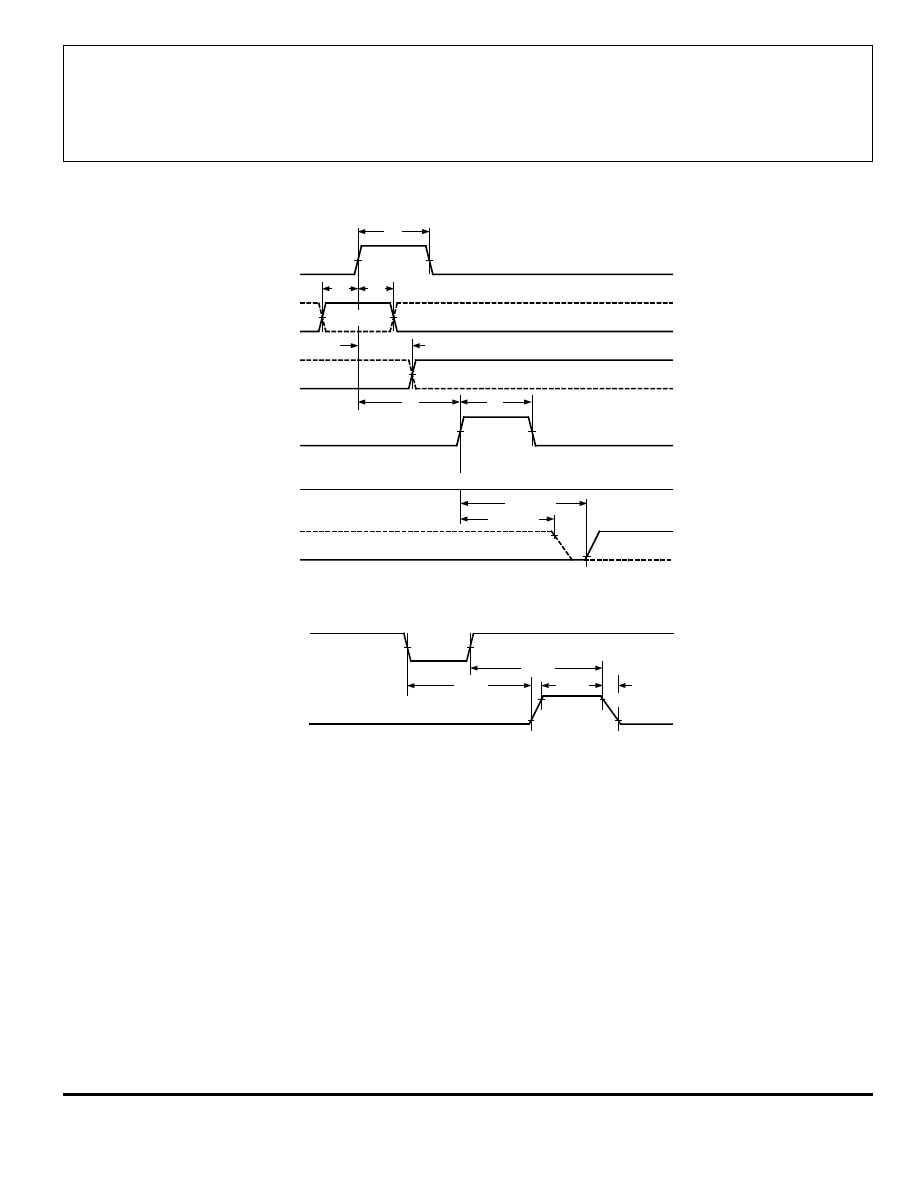
Serial Data present at the input is transferred to the shift
register on the logic “0” to logic “1” transition of the CLOCK
input pulse. On succeeding CLOCK pulses, the registers shift
data information towards the SERIAL DATA OUTPUT. The
SERIAL DATA must appear at the input prior to the rising edge
of the CLOCK input waveform.
Information present at any register is transferred to the
respective latch when the STROBE is high (serial-to-parallel
conversion). The latches will continue to accept new data as
long as the STROBE is held high. Applications where the
latches are bypassed (STROBE tied high) will require that the
BLANKING input be high during serial data entry.
When the BLANKING input is high, the output source
drivers are disabled (OFF); the pnp active pull-down sink
drivers are ON. The information stored in the latches is not
affected by the BLANKING input. With the BLANKING input
low, the outputs are controlled by the state of their respective
latches.
CLOCK
SERIAL
DATA IN
STROBE
BLANKING
OUT
N
Dwg. WP-029
50%
SERIAL
DATA OUT
DATA
DATA
10%
90%
50%
50%
50%
C
A
B
D
E
LOW = ALL OUTPUTS ENABLED
p(STH-QL)
t
p(CH-SQX)
t
DATA
p(STH-QH)
t
BLANKING
OUT
N
Dwg. WP-030
DATA
10%
50%
en(BQ)
t
dis(BQ)
t
HIGH = ALL OUTPUTS BLANKED (DISABLED)
90%
r
t
f
t
A. Data Active Time Before Clock Pulse
(Data Set-Up Time), t
su(D)
...................................... 25 ns
B. Data Active Time After Clock Pulse
(Data Hold Time), t
h(D)
............................................ 25 ns
C. Clock Pulse Width, t
w(CH)
............................................ 50 ns
D. Time Between Clock Activation and Strobe, t
su(C)
.... 100 ns
E. Strobe Pulse Width, t
w(STH)
.......................................... 50 ns
NOTE – Timing is representative of a 10 MHz clock. Higher
speeds may be attainable with increased supply voltage;
operation at high temperatures will reduce the specified
maximum clock frequency.
6812
20-BIT SERIAL-INPUT,
LATCHED SOURCE DRIVER
115 Northeast Cutoff, Box 15036
Worcester, Massachusetts 01615-0036 (508) 853-5000
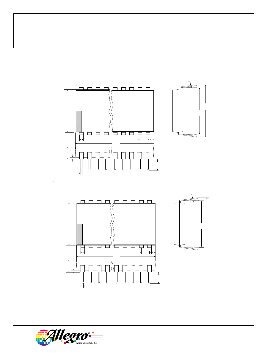
A6812EA, A6812KA, & A6812SA
Dimensions in Inches
(controlling dimensions)
Dimensions in Millimeters
(for reference only)
NOTES: 1. Exact body and lead configuration at vendor’s option within limits shown.
2. Lead spacing tolerance is non-cumulative.
3. Lead thickness is measured at seating plane or below.
4. Supplied in standard sticks/tubes of 12 devices.
28
1
2
3
0.250
MAX
0.070
0.030
0.015
MIN
0.022
0.014
0.015
0.008
0.600
BSC
Dwg. MA-003-28 in
14
0.100
BSC
0.005
MIN
0.200
0.115
4
0.700
MAX
15
1.565
1.380
0.580
0.485
28
14.73
12.32
1
2
3
6.35
MAX
1.77
0.77
0.39
MIN
0.558
0.356
0.381
0.204
15.24
BSC
Dwg. MA-003-28 mm
14
2.54
BSC
0.13
MIN
5.08
2.93
4
17.78
MAX
15
39.7
35.1
6812
20-BIT SERIAL-INPUT,
LATCHED SOURCE DRIVER
www.allegromicro.com
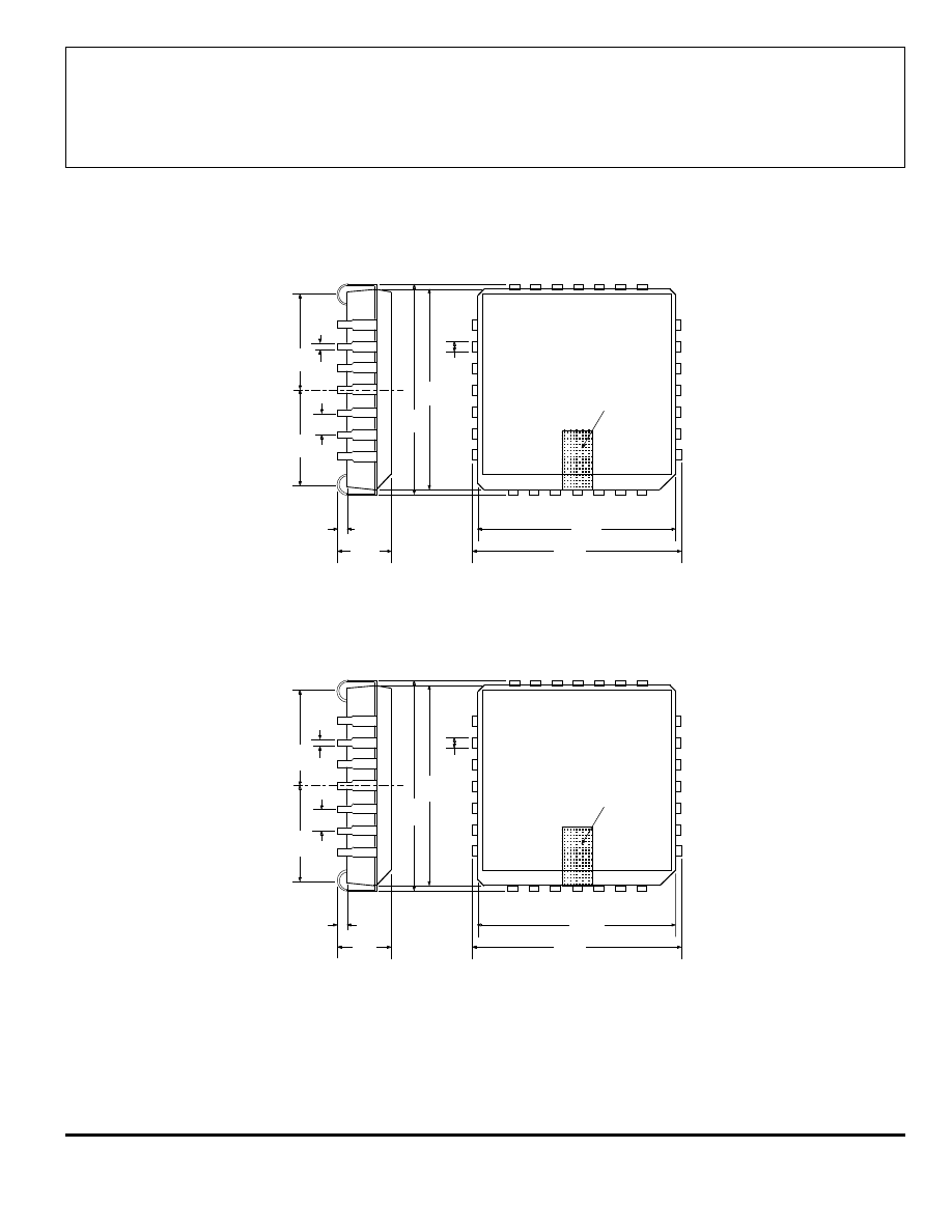
A6812EEP, A6812KEP, & A6812SEP
(add “TR” to part number for tape and reel)
Dimensions in Inches
(controlling dimensions)
NOTES: 1. Exact body and lead configuration at vendor’s option within limits shown.
2. Lead spacing tolerance is non-cumulative.
3. Supplied in standard sticks/tubes of 38 devices or add “TR” to part number for tape and reel.
18
12
0.020
MIN
0.050
BSC
1
28
INDEX AREA
Dwg. MA-005-28A in
0.026
0.032
0.013
0.021
26
25
19
11
4
5
0.165
0.180
0.495
0.485
0.456
0.450
0.495
0.485
0.456
0.450
0.219
0.191
0.219
0.191
0.51
MIN
4.57
4.20
1.27
BSC
12.57
12.32
11.582
11.430
1
28
INDEX AREA
Dwg. MA-005-28A mm
0.812
0.661
0.331
0.533
12.57
12.32
26
25
19
18
12
11
4
5
11.58
11.43
5.56
4.85
5.56
4.85
Dimensions in Millimeters
(for reference only))
6812
20-BIT SERIAL-INPUT,
LATCHED SOURCE DRIVER
115 Northeast Cutoff, Box 15036
Worcester, Massachusetts 01615-0036 (508) 853-5000
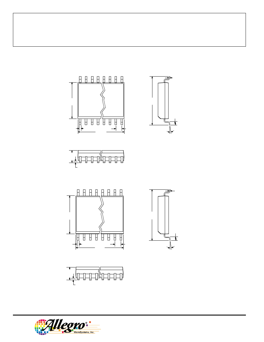
A6812ELW, A6812KLW, & A6812SLW
(add “TR” to part number for tape and reel)
Dimensions in Inches
(for reference only)
Dimensions in Millimeters
(controlling dimensions)
NOTES: 1. Exact body and lead configuration at vendor’s option within limits shown.
2. Lead spacing tolerance is non-cumulative.
3. Supplied in standard sticks/tubes of 27 devices or add “TR” to part number for tape and reel.
0
°
TO
8
°
1
28
2
3
18.10
17.70
0.51
0.33
2.65
2.35
0.10
MIN.
0.32
0.23
1.27
0.40
Dwg. MA-008-28A mm
1.27
BSC
15
7.60
7.40
10.65
10.00
0
°
TO
8
°
1
2
3
0.020
0.013
0.0040
MIN.
Dwg. MA-008-28A in
0.050
BSC
28
15
0.0125
0.0091
0.050
0.016
0.2992
0.2914
0.419
0.394
0.7125
0.6969
0.0926
0.1043

6812
20-BIT SERIAL-INPUT,
LATCHED SOURCE DRIVER
www.allegromicro.com
The products described here are manufactured under one or more
U.S. patents or U.S. patents pending.
Allegro MicroSystems, Inc. reserves the right to make, from time to
time, such departures from the detail specifications as may be
required to permit improvements in the performance, reliability, or
manufacturability of its products. Before placing an order, the user is
cautioned to verify that the information being relied upon is current.
Allegro products are not authorized for use as critical components
in life-support devices or systems without express written approval.
The information included herein is believed to be accurate and
reliable. However, Allegro MicroSystems, Inc. assumes no responsi-
bility for its use; nor for any infringement of patents or other rights of
third parties which may result from its use.
6812
20-BIT SERIAL-INPUT,
LATCHED SOURCE DRIVER
115 Northeast Cutoff, Box 15036
Worcester, Massachusetts 01615-0036 (508) 853-5000
POWER
INTERFACE DRIVERS
Function
Output Ratings*
Part Number†
SERIAL-INPUT LATCHED DRIVERS
8-Bit (saturated drivers)
-120 mA
50 V‡
5895
8-Bit
350 mA
50 V
5821
8-Bit
350 mA
80 V
5822
8-Bit
350 mA
50 V‡
5841
8-Bit
350 mA
80 V‡
5842
8-Bit (constant-current LED driver)
75 mA
17 V
6275
8-Bit (constant-current LED driver)
120 mA
24 V
6277
8-Bit (DMOS drivers)
250 mA
50 V
6595
8-Bit (DMOS drivers)
350 mA
50 V‡
6A595
8-Bit (DMOS drivers)
100 mA
50 V
6B595
10-Bit (active pull-downs)
-25 mA
60 V
5810-F and 6810
12-Bit (active pull-downs)
-25 mA
60 V
5811
16-Bit (constant-current LED driver)
75 mA
17 V
6276
20-Bit (active pull-downs)
-25 mA
60 V
5812-F and 6812
32-Bit (active pull-downs)
-25 mA
60 V
5818-F and 6818
32-Bit
100 mA
30 V
5833
32-Bit (saturated drivers)
100 mA
40 V
5832
PARALLEL-INPUT LATCHED DRIVERS
4-Bit
350 mA
50 V‡
5800
8-Bit
-25 mA
60 V
5815
8-Bit
350 mA
50 V‡
5801
8-Bit (DMOS drivers)
100 mA
50 V
6B273
8-Bit (DMOS drivers)
250 mA
50 V
6273
SPECIAL-PURPOSE DEVICES
Unipolar Stepper Motor Translator/Driver
1.25 A
50 V‡
5804
Addressable 8-Bit Decoder/DMOS Driver
250 mA
50 V
6259
Addressable 8-Bit Decoder/DMOS Driver
350 mA
50 V‡
6A259
Addressable 8-Bit Decoder/DMOS Driver
100 mA
50 V
6B259
Addressable 28-Line Decoder/Driver
450 mA
30 V
6817
*
Current is maximum specified test condition, voltage is maximum rating. See specification for sustaining voltage limits.
Negative current is defined as coming out of (sourcing) the output.
†
Complete part number includes additional characters to indicate operating temperature range and package style.
‡
Internal transient-suppression diodes included for inductive-load protection.
Wyszukiwarka
Podobne podstrony:
6812
6812
6812
praca magisterska 6812
6812
6812
6812
więcej podobnych podstron