TDA2009A
10 +10W STEREO AMPLIFIER
September 2003
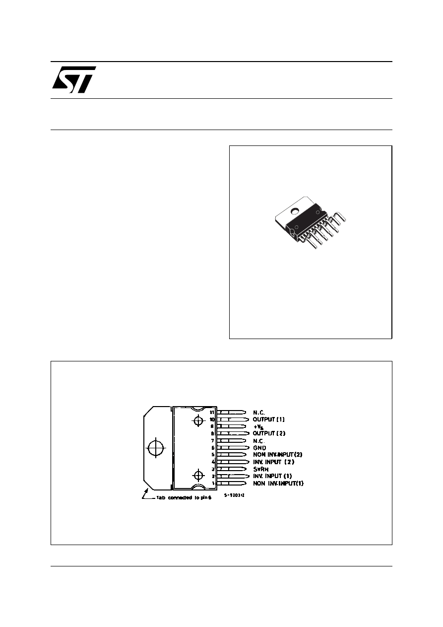
PIN CONNECTION
MULTIWATT11
ORDERING NUMBER : TDA2009A
®
.
HIGH OUTPUT POWER
(10 + 10W Min. @ D = 1%)
.
HIGH CURRENT CAPABILITY (UP TO 3.5A)
.
AC SHORT CIRCUIT PROTECTION
.
THERMAL OVERLOAD PROTECTION
.
SPACE AND COST SAVING : VERY LOW
NUMBER OF EXTERNAL COMPONENTS
AND SIMPLE MOUNTING THANKS TO THE
MULTIWATT
PACKAGE.
DESCRIPTION
The TDA2009A is class AB dual Hi-Fi Audio power
amplifier assembled in Multiwatt
package, spe-
cially designed for high quality stereo application
as Hi-Fi and music centers.
1/12
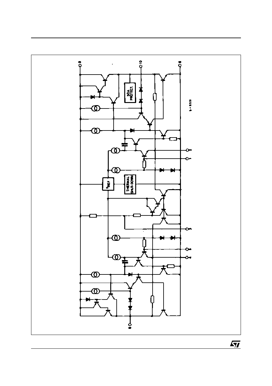
SCHEMATIC DIAGRAM
TDA2009A
2/12
ABSOLUTE MAXIMUM RATINGS
Symbol
Parameter
Value
Unit
V
s
Supply Voltage
28
V
I
o
Output Peak Current (repetitive f
≥
20 Hz)
3.5
A
I
o
Output Peak Current (non repetitive, t = 100
µ
s)
4.5
A
P
tot
Power Dissipation at T
case
= 90
°
C
20
W
T
stg,
T
j
Storage and Junction Temperature
– 40, + 150
°
C
THERMAL DATA
Symbol
Parameter
Value
Unit
R
th j-case
Thermal Resistance Junction-case
Max.
3
°
C/W
ELECTRICAL CHARACTERISTICS
(refer to the stereo application circuit, T
amb
= 25
o
C, V
S
= 24V, G
V
= 36dB, unless otherwise specified)
Symbol
Parameter
Test Conditions
Min.
Typ. Max.
Unit
V
s
Supply Voltage
8
28
V
V
o
Quiescent Output Voltage
V
s
= 24V
11.5
V
I
d
Total Quiescent Drain Current
V
s
= 24V
60
120
mA
P
o
Output Power (each channel)
d = 1%, V
s
= 24V, f = 1kHz
R
L
= 4
Ω
R
L
= 8
Ω
f = 40Hz to 12.5kHz
R
L
= 4
Ω
R
L
= 8
Ω
V
s
= 18V, f = 1kHz
R
L
= 4
Ω
R
L
= 8
Ω
10
5
12.5
7
7
4
W
W
W
W
W
W
d
Distortion (each channel)
f = 1kHz, V
s
= 24V
P
o
= 0.1 to 7W
R
L
= 4
Ω
P
o
= 0.1 to 3.5W
R
L
= 8
Ω
V
s
= 18V
P
o
= 0.1 to 5W
R
L
= 4
Ω
P
o
= 0.1 to 2.5W
R
L
= 8
Ω
0.2
0.1
0.2
0.1
%
%
%
%
CT
Cross Talk (3)
R
L
=
∞
, R
g
= 10k
Ω
f = 1kHz
f = 10kHz
60
50
dB
V
i
Input Saturation Voltage (rms)
300
mV
R
i
Input Resistance
f = 1kHz, Non Inverting Input
70
200
k
Ω
f
L
Low Frequency Roll off (– 3dB)
R
L
= 4
Ω
20
Hz
f
H
High Frequency Roll off (– 3dB)
R
L
= 4
Ω
80
kHz
G
v
Voltage Gain (closed loop)
f = 1kHz
35.5
36
36.5
dB
∆
G
v
Closed Loop Gain Matching
0.5
dB
e
N
Total Input Noise Voltage
R
g
= 10k
Ω
(1)
R
g
= 10k
Ω
(2)
1.5
2.5
8
µ
V
µ
V
SVR
Supply Voltage Rejection (each channel)
R
g
= 10k
Ω
f
ripple
= 100Hz, V
ripple
= 0.5V
55
dB
T
J
Thermal Shut-down Junction Temperature
145
°
C
Notes :
1.
Curve A
2.
22Hz to 22kHz
TDA2009A
3/12
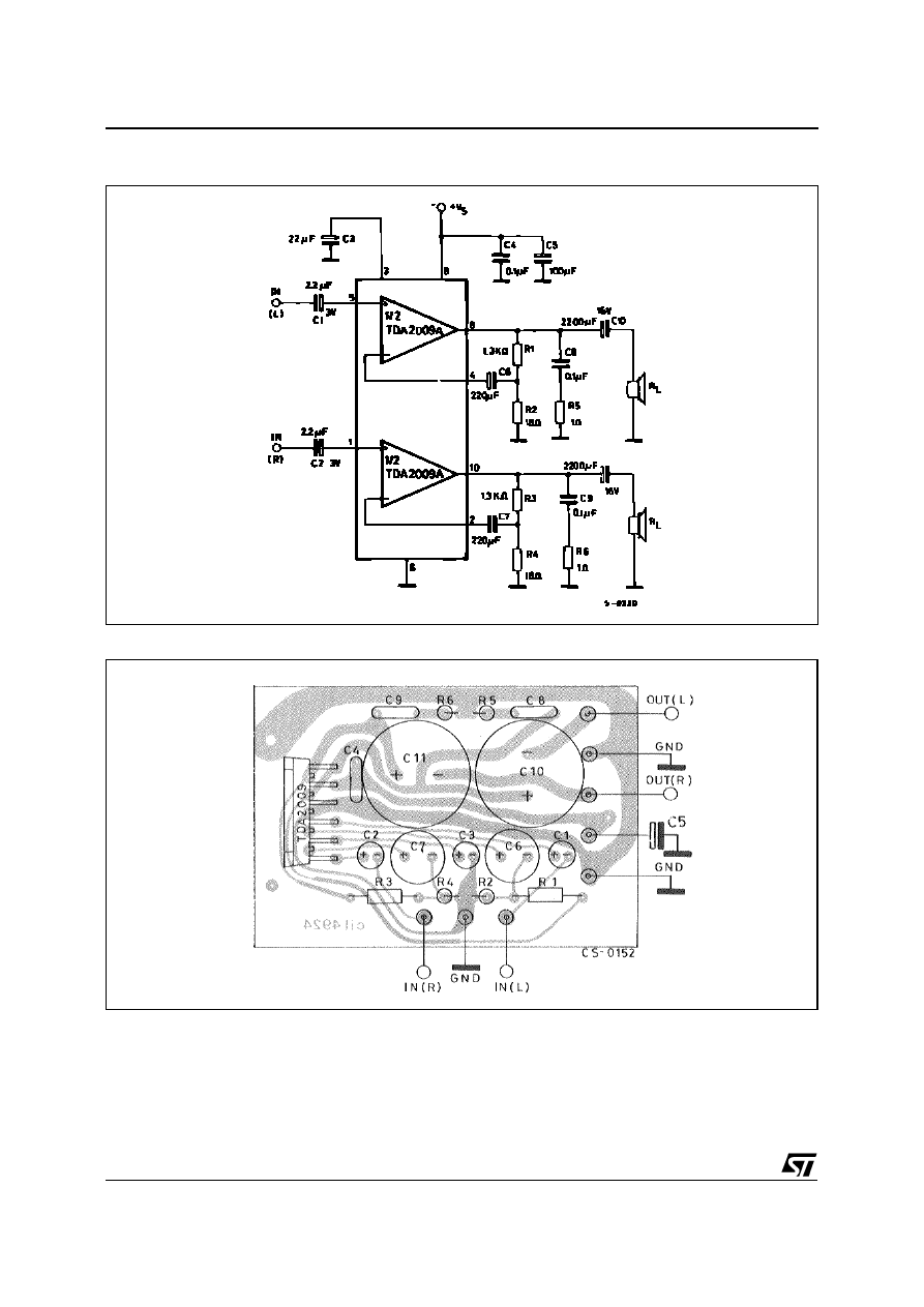
Figure 1 : Test and Application Circuit (G
V
= 36dB)
Figure 2 : P.C. board and component layout of the fig. 1
TDA2009A
4/12
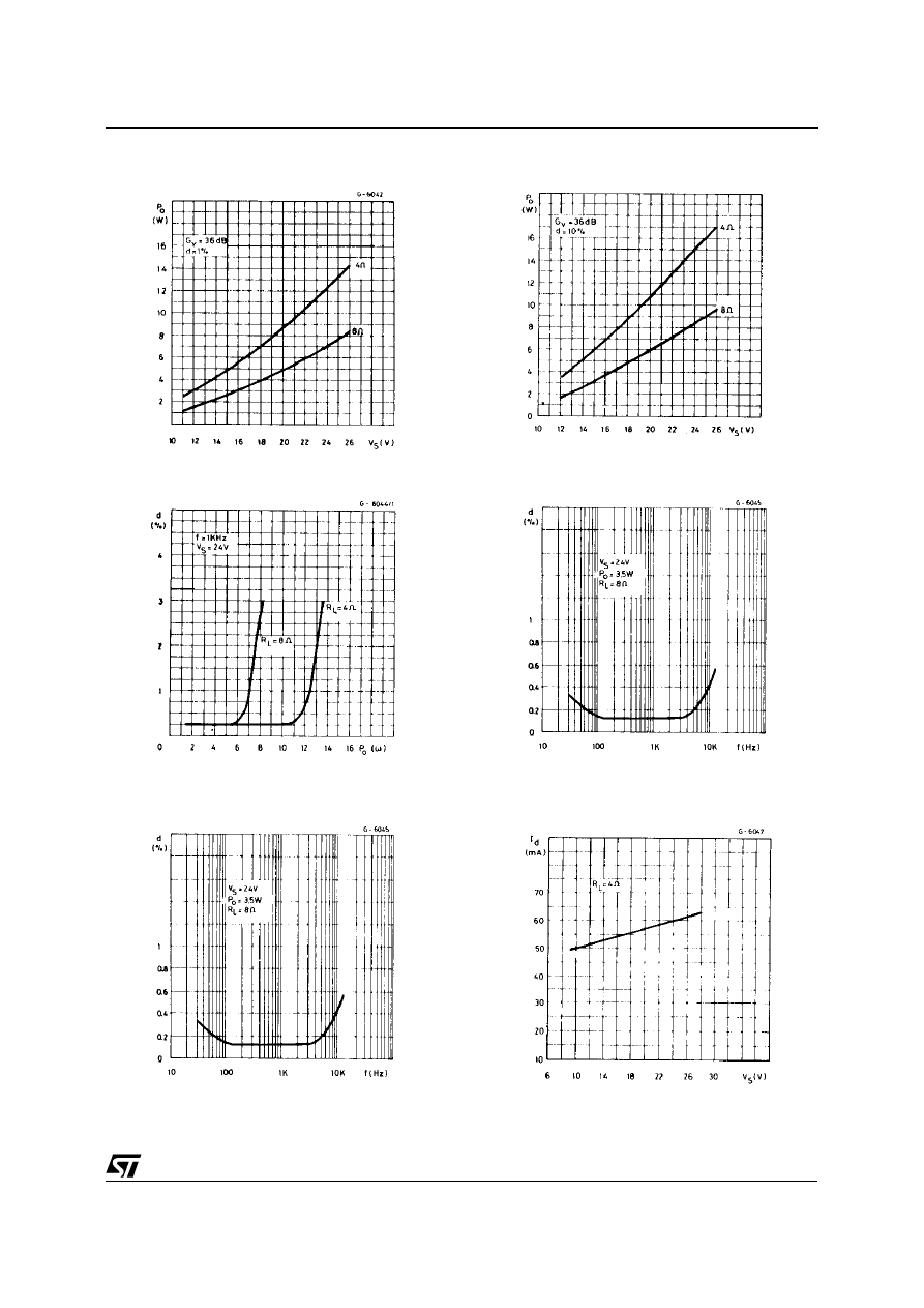
Figure 3 :
Output Power versus Supply Voltage
Figure 4 :
Output Power versus Supply Voltage
Figure 5 :
Distortion versus Output Power
Figure 6 :
Distortion versus Frequency
Figure 7 :
Distortion versus Frequency
Figure 8 :
Quiescent Current versus
Supply Voltage
TDA2009A
5/12
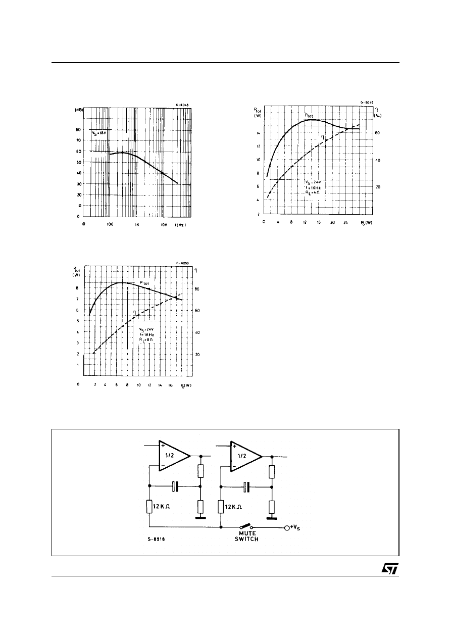
Figure 9 :
Supply Voltage Rejection versus
Frequency
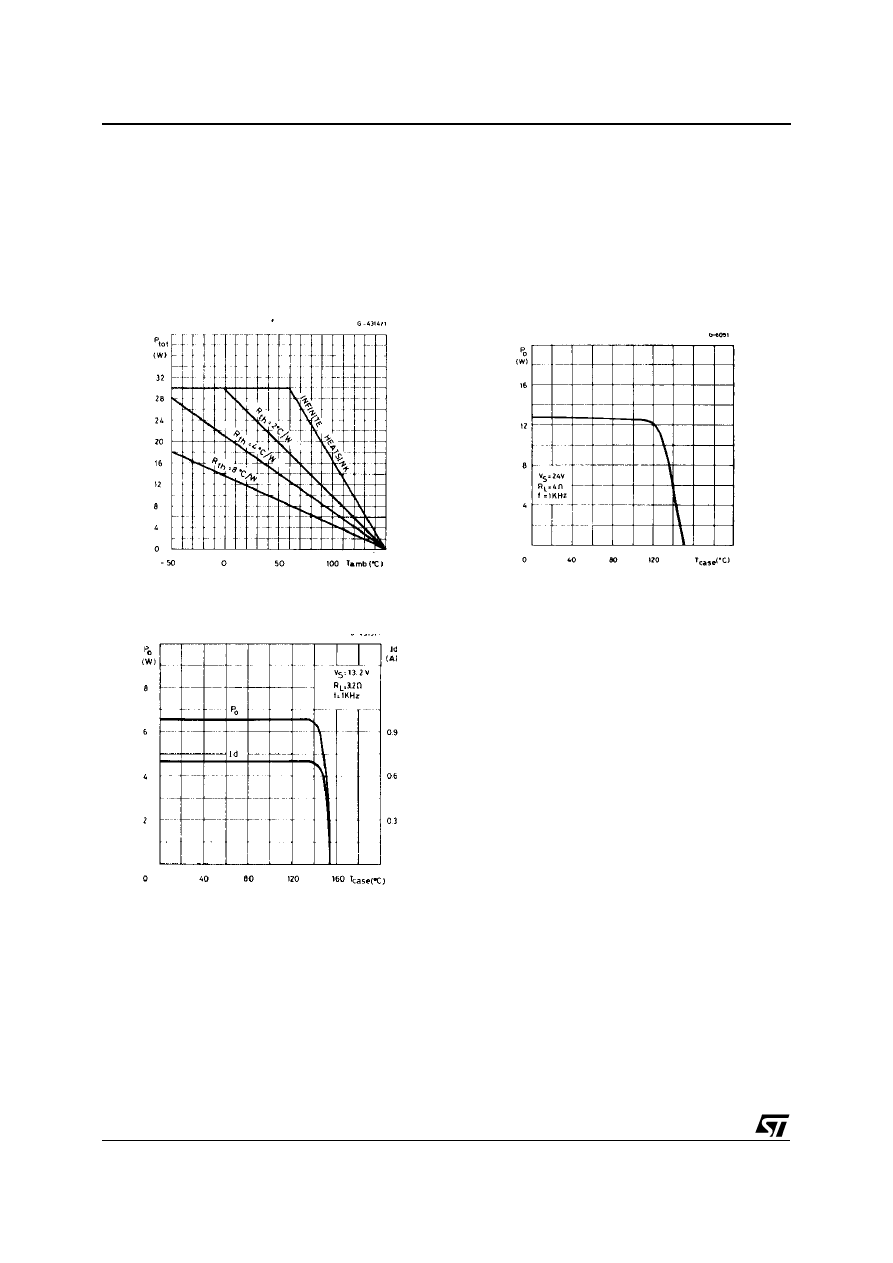
Figure 10 : Total Power Dissipation and
Efficiency versus Output Power
Figure 11 : Total Power Dissipation and
Efficiency versus Output Power
APPLICATION INFORMATION
Figure 12 : Example of Muting Circuit
TDA2009A
6/12
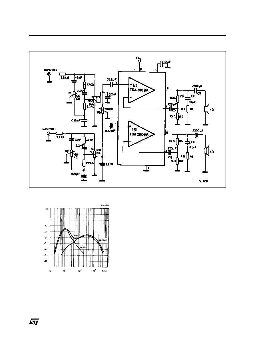
Figure 13 : 10W +10W Stereo Amplifier with Tone Balance and Loudness Control
Figure 14 : Tone Control Response
(circuit of Figure 13)
TDA2009A
7/12
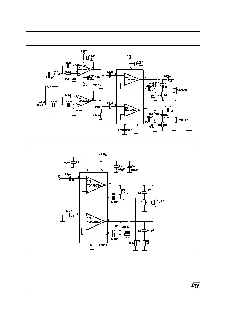
Figure 15 : High Quality 20 + 20W Two Way Amplifier for Stereo Music Center (one channel only)
Figure 16 : 18W Bridge Amplifier (d = 1%, G
V
= 40dB)
TDA2009A
8/12
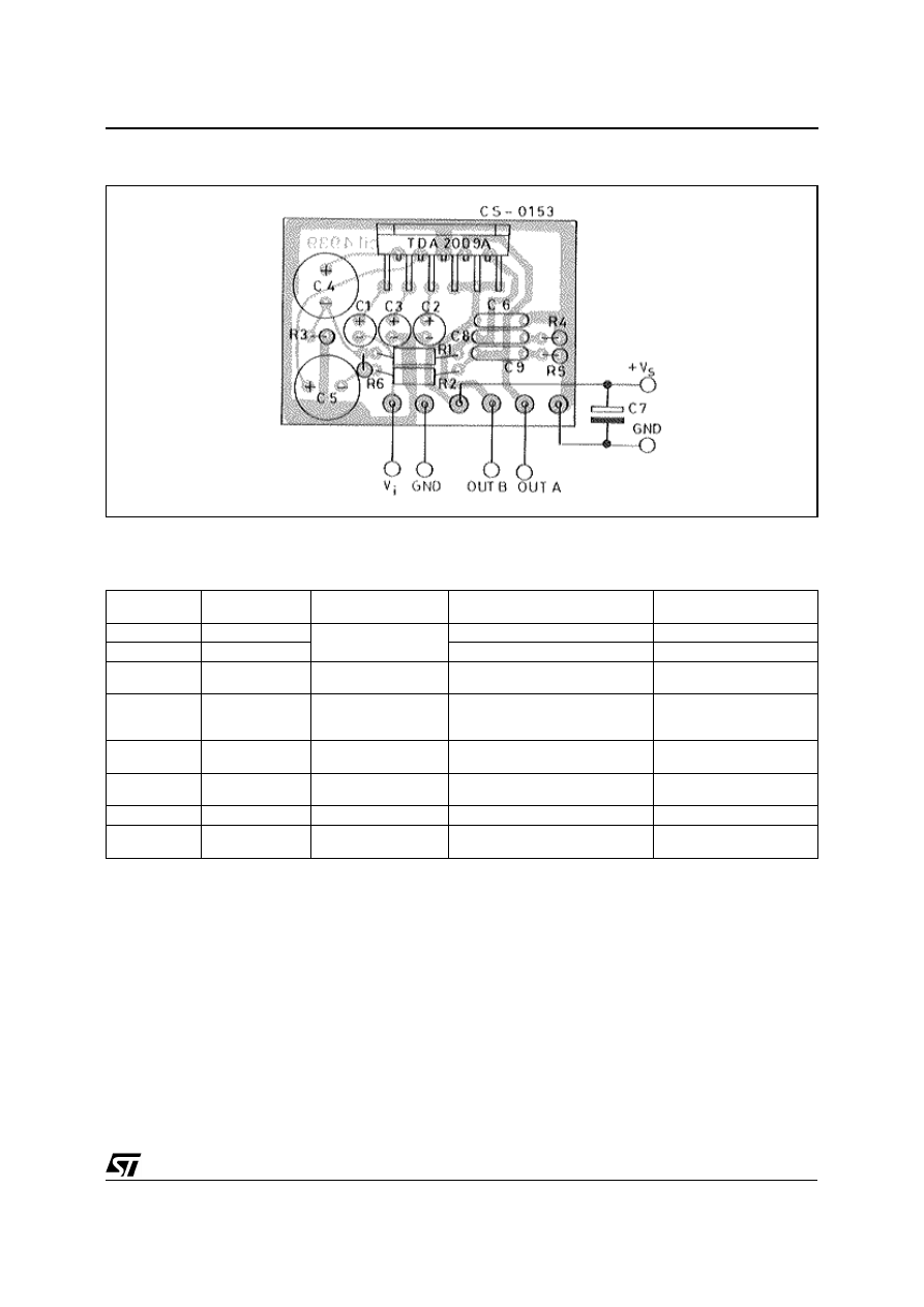
Figure 17 : P.C. BOARD and Components Layout of the Circuit of Figure 16 (1:1 scale)
APPLICATION SUGGESTION
The recommended values of the components are those shown on application circuit of fig. 1. Different
values can be used ; the following table can help the designer.
Component
Recommended
Value
Purpose
Larger than
Smaller than
R1, R3
1.2k
Ω
Close Loop Gain
Setting (1)
Increase of Gain
Decrease of Gain
R2, R4
18k
Ω
Decrease of Gain
Increase of Gain
R5, R6
1
Ω
Frequency Stability
Danger of Oscillation at High
Frequency with Inductive Load
C1, C2
2.2
µ
F
Input DC Decoupling
High Turn-on Delay
High Turn-on Pop.
Higher Low Frequency
Cut-off. Increase of Noise
C3
22
µ
F
Ripple Rejection
Better SVR. Increase of the
Switch-on Time
Degradation of SVR
C6, C7
220
µ
F
Feedback Input DC
Decoupling
C8, C9
0.1
µ
F
Frenquency Stability
Danger of Oscillation
C10, C11
1000
µ
F to
2200
µ
F
Output DC
Decoupling
Higher Low-frequency
Cut-off
(1) The closed loop gain must be higher than 26dB.
The presence of a thermal limiting circuit offers the
following advantages:
1) an averload on the output (even if it is
per m a nen t ) , or an ex ces si ve am bient
temperature can be easily withstood.
2) the heatsink can have a smaller factor of safety
compared with that of a conventional circuit.
There is no device damage in the case of
excessive junction temperature : all that
happens is that P
o
(and therefore P
tot
) and I
o
are
reduced.
The maximum allowable power dissipation de-
pends upon the size of the external heatsink (i.e.
its thermal resistance); Figure 18 shows this dissi-
pable power as a function of ambient temperature
for different thermal resistance.
Short circuit (AC Conditions). The TDA2009A can
withstand an accidental short circuit from the output
and ground made by a wrong connection during
normal play operation.
BUILD-IN PROTECTION SYSTEMS
THERMAL SHUT-DOWN
TDA2009A
9/12
The power dissipated in the circuit must be re-
moved by adding an external heatsink.
Thanks to the MULTIWATT
package attaching
the heatsink is very simple, a screw or a compres-
sion spring (clip) being sufficient. Between the
heatsink and the package it is better to insert a layer
of silicon grease, to optimize the thermal contact ;
no electrical isolation is needed between the two
MOUNTING INSTRUCTIONS
Figure 18 : Maximum Allowable Power Dissipa-
tion versus Ambient Temperature
Figure 19 : Output Power versus Case
Temperature
Figure 20 : Output Power and Drain Current ver-
sus Case Temperature
TDA2009A
10/12
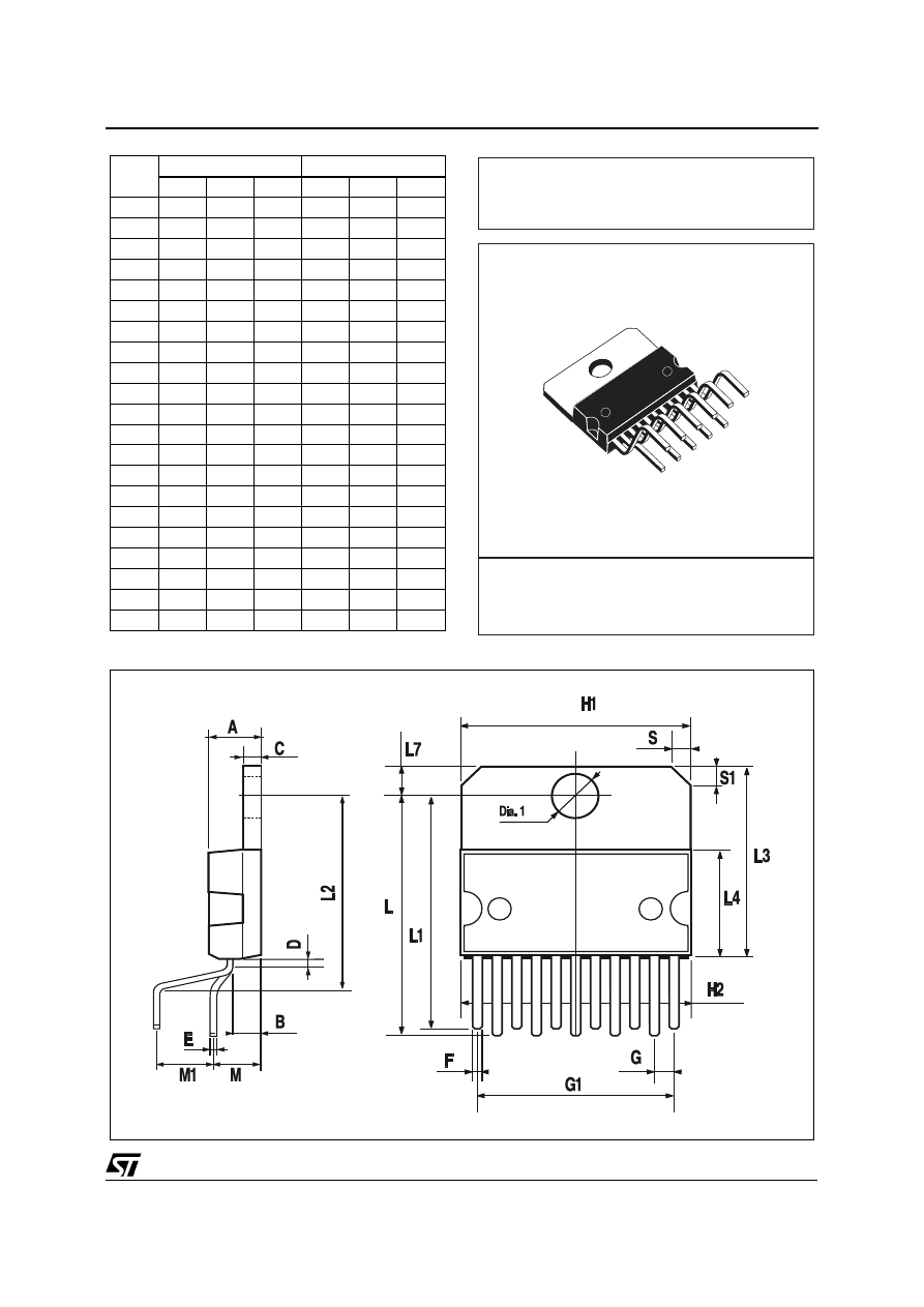
Multiwatt11 V
DIM.
mm
inch
MIN.
TYP.
MAX.
MIN.
TYP.
MAX.
A
5
0.197
B
2.65
0.104
C
1.6
0.063
D
1
0.039
E
0.49
0.55
0.019
0.022
F
0.88
0.95
0.035
0.037
G
1.45
1.7
1.95
0.057
0.067
0.077
G1
16.75
17
17.25
0.659
0.669
0.679
H1
19.6
0.772
H2
20.2
0.795
L
21.9
22.2
22.5
0.862
0.874
0.886
L1
21.7
22.1
22.5
0.854
0.87
0.886
L2
17.4
18.1
0.685
0.713
L3
17.25
17.5
17.75
0.679
0.689
0.699
L4
10.3
10.7
10.9
0.406
0.421
0.429
L7
2.65
2.9
0.104
0.114
M
4.25
4.55
4.85
0.167
0.179
0.191
M1
4.73
5.08
5.43
0.186
0.200
0.214
S
1.9
2.6
0.075
0.102
S1
1.9
2.6
0.075
0.102
Dia1
3.65
3.85
0.144
0.152
OUTLINE AND
MECHANICAL DATA
TDA2009A
11/12

Information furnished is believed to be accurate and reliable. However, STMicroelectronics assumes no responsibility for the
consequences of use of such information nor for any infringement of patents or other rights of third parties which may result from
its use. No license is granted by implication or otherwise under any patent or patent rights of STMicroelectronics. Specifications
mentioned in this publication are subject to change without notice. This publication supersedes and replaces all information
previously supplied. STMicroelectronics products are not authorized for use as critical components in life support devices or systems
without express written approval of STMicroelectronics.
The ST logo is a registered trademark of STMicroelectronics.
All other names are the property of their respective owners
© 2003 STMicroelectronics - All rights reserved
STMicroelectronics GROUP OF COMPANIES
Australia – Belgium - Brazil - Canada - China – Czech Republic - Finland - France - Germany - Hong Kong - India - Israel - Italy - Ja-
pan - Malaysia - Malta - Morocco - Singapore - Spain - Sweden - Switzerland - United Kingdom - United States
www.st.com
TDA2009A
12/12
Wyszukiwarka
Podobne podstrony:
TDA2007A STMicroelectronics elenota pl
TDA2002 STMicroelectronics elenota pl
TDA7388 STMicroelectronics elenota pl
TDA7383 STMicroelectronics elenota pl
TDA7566 STMicroelectronics elenota pl
TDA7266M STMicroelectronics elenota pl
TDA7850 STMicroelectronics elenota pl
TDA7490LSA STMicroelectronics elenota pl
TDA1908 STMicroelectronics elenota pl (1)
TDA7233 STMicroelectronics elenota pl
TDA7231A STMicroelectronics elenota pl
TDA7360 STMicroelectronics elenota pl
TDA7386 STMicroelectronics elenota pl (2)
TDA7385 STMicroelectronics elenota pl
TDA7490SA STMicroelectronics elenota pl
TDA7370B STMicroelectronics elenota pl
TDA7266S STMicroelectronics elenota pl
więcej podobnych podstron