PCBA Debug Guide
Página 1 de 10
Rev. 2.8
PCIE Faults
Debug Guide
Rev 2.8
PCBA Debug Guide
Página 2 de 10
Rev. 2.8
1. Revision History
Revision
Description
Author/Revised
By
Date
1.0
Draft release
Luis Rodríguez
14 0ct 2005
2.0
Category C added
Luis Rodríguez
24 Jan 2006
2.1
Updated category B
(Refer to the table)
(Modified the components to replace with
the CPUs bits 00010101: U4D1 instead of
U2E1 for the 1
st
repair, U7D1 instead of
U2C1 in the 2
nd
repair and there are no 3
rd
repair)
Luis Rodríguez
José C. Bravo
06 Mar 2006
2.2
Updated category B
(Refer to the table)
(Added 2
nd
and 3
rd
repair in failures with
CPUs bits 01000100)
Luis Rodriguez
José C. Bravo
08 Mar 2006
2.3
Updated category B
(Refer to the table)
(Added repair action for CPU bits
00000000)
Luis Rodriguez
José C. Bravo
09 Mar 2006
2.4
Updated category B
(Refer to the table)
(Added repair action for CPU bits
10101111)
Luis Rodriguez
José C. Bravo
22 Mar 2006
2.5
Updated category B
(Refer to the table)
(Added repair action for CPU bits 01010001
& 10110011)
Luis Rodriguez
José C. Bravo
04 April 2006
2.6
Updated category B
(Refer to the table)
(Added repair action for CPU bits
10010110)
Luis Rodriguez
José C. Bravo
09 May 2006
2.7
Updated category A & C
(Added replacement of component in first
repair U2C1 & in second repair U4D1 in
category A )
(Added replacement of component in first
repair: U4D1 in category C)
Luis Rodriguez
José C. Bravo
14 July 2006
2.8
Updated category B & C
(Refer to the table)
(Added repair action for CPU bits
00100000, 01000101, 01001111,
10010100,
01011000, 10101101 &
10100010)
(Added replacement of component in first
repair: Fault Infineon R3G6 & R3G7)
Moisés Anzaldo
28 July 2006
PCBA Debug Guide
Página 3 de 10
Rev. 2.8
2. Table of Contents
1. Revision History ......................................................................................................................... 2
2. Table of Contents........................................................................................................................ 3
3. Introduction................................................................................................................................. 3
4. Scope.......................................................................................................................................... 3
5. Audience ..................................................................................................................................... 3
6. Process ........................................................................................................................................ 4
7. Category Grouping...................................................................................................................... 4
7.2 Category A Error Code 0x09................................................................................................ 4
7.2 Category B Error Code 0x0A ............................................................................................... 6
7.3 Category C Error Code 0x08................................................................................................ 9
3. Introduction
This document describes a process for diagnosing and repairing NO PCIE failures from
the PCBA tester. The process and groupings below outlines possible measurements to
determine the appropriate component, for repair or replacement. Core digital errors can
also be identified by 3 of the 4 LEDs on the “ring of light” flashing.
4. Scope
This document has been developed from experience gained on X803158-001 Xenon
XDK motherboards. The failure analysis process outlined in this document should be
used in conjunction with the “Motherboard Debug Guide Development Process”
document.
5. Audience
This document is aimed at Engineers and Technicians who are performing first pass
debug of core digital failures from the XBOX360 motherboard PCBA tester.

PCBA Debug Guide
Página 4 de 10
Rev. 2.8
6. Process
7. Category Grouping
Note: Error Codes on front panel are in hexadecimal: 0x
FF
Error Codes in the Functional Test are shown with 8 digits: 0x
12345678
Bits get on the PCBA test points are 8 digits:
01010101
7.2 Category A Error Code 0x09
The PCI-E link failed to enter L0 in time during seqUnReset
Test Name: PowerGroupPowerUp, Variation: PCBA-TighterLimits
Error Code: 0x81600868
Error Facility: TESTER (FACILITY_MTE_POWER)
Error Description: Measured value lower than limit V12_CURRENT: 5.963584 less than
6.500000
Test Name: PowerGroupPowerUp, Variation: PCBA-TighterLimits
Error Code: 0x81600BE5
Error Facility: TESTER (FACILITY_MTE_POWER)
Error Description: The PCI-E link failed to enter L0 in time during seqUnReset. SMC
ErrorCode: 9
Replace U2C1 as a first repair
Replace U4D1 as a second repair
If the failure is still present, continue next repairs
•
Check for proper voltage on V_GPUPCIE (U5C1 pin2), target is 1.25v, if
not present change U5U1
•
Check for proper voltage on V_SBPCIE (U3P1 pin 2), target is 1.87v, if not
present change U3P1
•
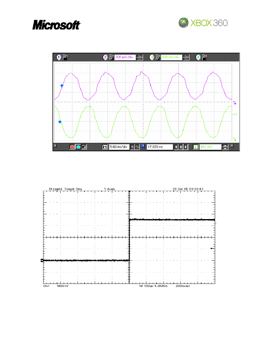
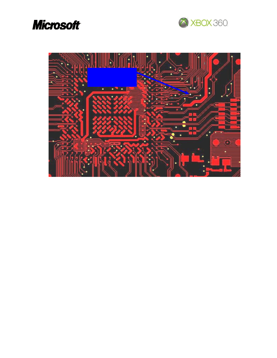
Check for PCIE CLK
•
PCIE_CLK_DP on FT3P2, frequency of 100MHz
•
PCIE_CLK_DN on FT3P1, frequency of 100MHz, as shown below
•
Check C2C1, C2C2, C2C3, C2C4, C4D1, C4D2, C4D3 & C5D1
•
Check GPU_CLK_DP/DN, frequency of 100MHz (junction between
R3C16 & R3C15)
PCBA Debug Guide
Página 5 de 10
Rev. 2.8
PCIEX_CLK_DP
PCIEX_CLK_DN
If frequencies are not present then change U3B4
•
Check CPU_RST_N (R7R4 pin 2) target is 1.24v, if not voltage change
U2C1
CPU_RST_N
PCBA Debug Guide
Página 6 de 10
Rev. 2.8
CPU_RST_N (via
near U2C1)
7.2 Category B Error Code 0x0A
Test Name: TcsBootStrappingDuration, Variation: PCBA
Error Code: 0x81510027
At this point of failure the V_CPUCORE is good, the PCI-E link has entered into a
known good state, and the SMC releases the CPU reset line CPU_RST_N.
CPU_RST_N is expected to go high. The SMC monitors the CPU initialization process
as it comes out of reset and begins to execute code. If the CPU fails to initialize properly
the SMC will enter the error state ERROR_NO_HANDSHAKE.
A typical problem found with this failure is that CPU programming code in flash is
corrupted. The CPU initializes and begins executing code from flash and falls on its
face. Change the Flash as a first repair.
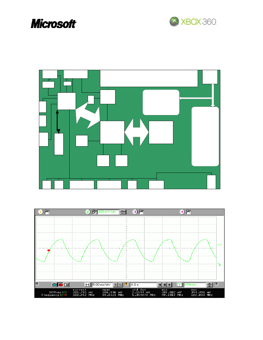
The CPU accesses flash through the path of CPU Chip ↔ Front Side Bus ↔ North
Bridge chip ↔ Back Side Bus ↔ South Bridge chip ↔ Flash chip. See picture below.
Failure along any segment of this path will cause ERROR_NO_HANDSHAKE as the
CPU cannot execute code from flash.
PCBA Debug Guide
Página 7 de 10
Rev. 2.8
Note
: At this early time the SMC does not double check the status of the Back Side Bus (BSB)
after a failure of the CPU to handshake. (A failure of the BSB is indicated with the previous error
code ERROR_NO_PCIE). It is possible that the BSB has failed after initial good status.
CPU
GPU
North
Bridge
RAM
RAM
RAM
South
Bridge
SMC
ANA
LAN/USB
Connector
LAN
AV Connector
Audio
DAC
Clock
Gen
FLA
S
H
HDD
SATA
ODD
Pwr
ODD
SAT
A
Eject
Switch
IR
Rx
USB Memory
Connector
USB Memory
Connector
Binding
Button
Argon
Connector
USB
Game
Pad
Power
Supply
Connector
FAN ASSEMBLY
Front
Side Bus
Bac
k S
ide
Bus
GPU
Voltage Regulators
CPU
Voltage
Regulators
SPDIF
• Check for proper control and power good signals.
CPU Clock Signal
PCBA Debug Guide
Página 8 de 10
Rev. 2.8
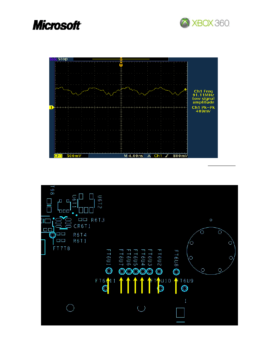
If CPU CLK (junction between R3C12 & R3C18) is not present or the signal is bad (e.g.
picture below), replace U3B4 as a first repair.
• If ENET_RST_N (boards with U1B2) & AUD_RST_N signals are not present and
the others are normal, change U7D1.
Bad CPU Clock Signal
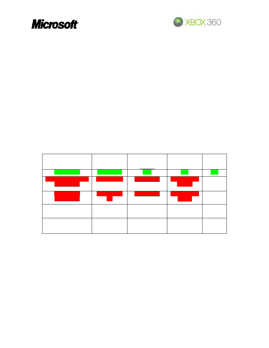
CPU Bits:
Bit: 0 1 2 3 4 5 6 7
PCBA Debug Guide
Página 9 de 10
Rev. 2.8
Do measures on the test points behind U7D1 (bottom side)
e.g.
Bits order: 76543210
Value 64: 01000000
Value 175:10101111
Front panel Code
CPU bits
1
st
repair
2
nd
repair
3
rd
repair
00000000
(0)
U7D1
00010100
(20)
U4D1 U7D1
00010101
(21)
U4D1
U7D1
00010110
(22)
U4D1 U7D1
00011000
(24)
U4D1 U7D1
00100000
(32)
U7D1
00101110
(46)
U4D1 U7D1
01000000
(64)
U3E1 U3D1
U4D1
01000100
(68)
U5F1/U5U1
U3E1/U3T1
U3D1/U3R1
01000101
(69)
U3D1/U3R1
U3E1/U3T1
U5F1/U5U1
01001111
(79)
U2E1
U7D1
01010001
(81)
U2E1
01011000
(88)
U2E1
10010100
(148)
U4D1
10010110
(150)
U2E1
U4D1
10101101
(153)
U2E1
10100010
(162)
U2E1
10101111
(175)
U4D1
U4F1/U4U1
0x0A
10110011
(179)
U2E1
7.3 Category C Error Code 0x08
Replace U4D1 as a first repair
PCBA Debug Guide
Página 10 de 10
Rev. 2.8
If the failure is still present, continue next repairs
•
Check for proper voltage on V_GPUPCIE (U5C1 pin2), target is 1.25v, if
not present change U5U1 (first check V_3P3 on U1F1 pin 4 replace as
necessary)
•
Check for proper voltage on V_SBPCIE (U3P1 pin 2), target is 1.87v, if not
present change U3P1
•
Check voltage V_MEM on DB3F1, expected value 1.8v, if the voltage is
not present: Measure resistance to GND, the expected value is 63Ω, if the
resistance is ok then check the signal VREG_1P8_EN on junction
between R3G5 & R3G1, in STBY mode is high, when the console is
turned on the signal goes low, this signal comes from the South Bridge if
is not present replace U2C1, if is present replace U4V1
•
Fault because of the voltage V_MEM altered in units with memories
Infineon
Impedance
between R3G6&
R3G7 a GND
Voltage in DB3F1
For memory
Infineon
Repair without
short in
DB3F1&GND
front panel
code
Normal value
600Ω a 800Ω
2.1V
N/A
N/A
Elevates R3G6& R3G7
No connected
Bigger a 5K Ω
No connected
Replace R3G6
& R3G7
Elevate R3G6
No connected
1.17kΩ a 1.49
kΩ
No connected
Replace R3G6
y R3G7
Elevate R3G7
2.20 kΩ a 2.40
kΩ
0.7V
Replace R3G6
y R3G7
0X08
Inverted
R3G6& R3G7
908Ω a 912 Ω 1.30V
Replace R3G6
y R3G7
0X08
Any another value of impedance between R3G6 & R3G7 a GND replace
R3G6 & R3G7
Note
: Units with memories Infineon first check R3G6 & R3G7 for a possible
bad repair, if the impedance on nodes V_MEM to GND is less than 5Ω (with
front panel code 0X08 or 0X14) replace memories and the GPU
•
If the impedance on these nodes (V_MEM & GND) is less than 50Ω
replace memories
•
If the impedance on these nodes (V_MEM & GND) is less than 0.3Ω
check in X- ray test memory and GPU possible short, change integrated in
short.
Document Outline
- 1. Revision History
- 2. Table of Contents
- 3. Introduction
- 4. Scope
- 5. Audience
- 6. Process
- 7. Category Grouping
Wyszukiwarka
Podobne podstrony:
Zamówienia publiczne, 104PROTOKÓŁ pow. prog. NO v2, oznaczenie sprawy
64GB ALL KILLER NO FILLER EDITION V2
DTC v2
No Home, No Homeland raport
NO 04 A004 4 2010
Elektro (v2) poprawka
l1213 r iMiBM lakei v2
logika rozw zadan v2
poprawkowe, MAD ep 13 02 2002 v2
Chopin Bourrée No 2, Op D2 No 2
DSC PC5010 v2 0 obs lcd
87 Dz U 08 25 150 Prawo ochrony środowiska v2
DSC PC5010 v2 0 ark
No Longer White
więcej podobnych podstron