TL/F/5991
CD4511BM/CD4511BC
BCD-to-7
Segment
Latch/Decoder/Driver
February 1988
CD4511BM/CD4511BC BCD-to-7 Segment
Latch/Decoder/Driver
General Description
The CD4511BM/CD4511BC BCD-to-seven segment latch/
decoder/driver is constructed with complementary MOS
(CMOS) enhancement mode devices and NPN bipolar out-
put drivers in a single monolithic structure. The circuit pro-
vides the functions of a 4-bit storage latch, an 8421 BCD-to-
seven segment decoder, and an output drive capability.
Lamp test (LT), blanking (BI), and latch enable (LE) inputs
are used to test the display, to turn-off or pulse modulate
the brightness of the display, and to store a BCD code,
respectively. It can be used with seven-segment light emit-
ting diodes (LED), incandescent, fluorescent, gas discharge,
or liquid crystal readouts either directly or indirectly.
Applications include instrument (e.g., counter, DVM, etc.)
display driver, computer/calculator display driver, cockpit
display driver, and various clock, watch, and timer uses.
Features
Y
Low logic circuit power dissipation
Y
High current sourcing outputs (up to 25 mA)
Y
Latch storage of code
Y
Blanking input
Y
Lamp test provision
Y
Readout blanking on all illegal input combinations
Y
Lamp intensity modulation capability
Y
Time share (multiplexing) facility
Y
Equivalent to Motorola MC14511
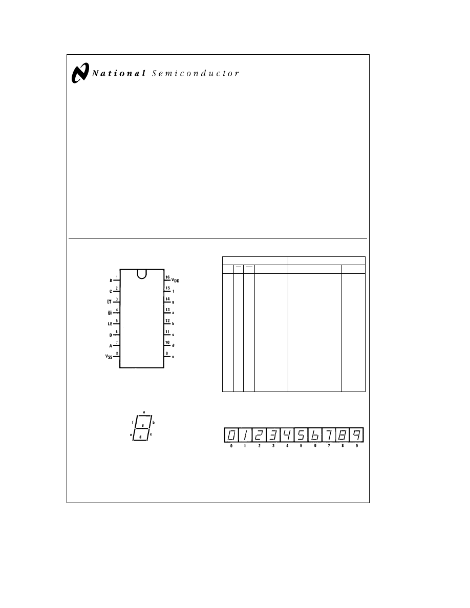
Connection Diagram
Dual-In-Line Package
TL/F/5991 – 1
Top View
Order Number CD4511B
Segment Identification
TL/F/5991 – 3
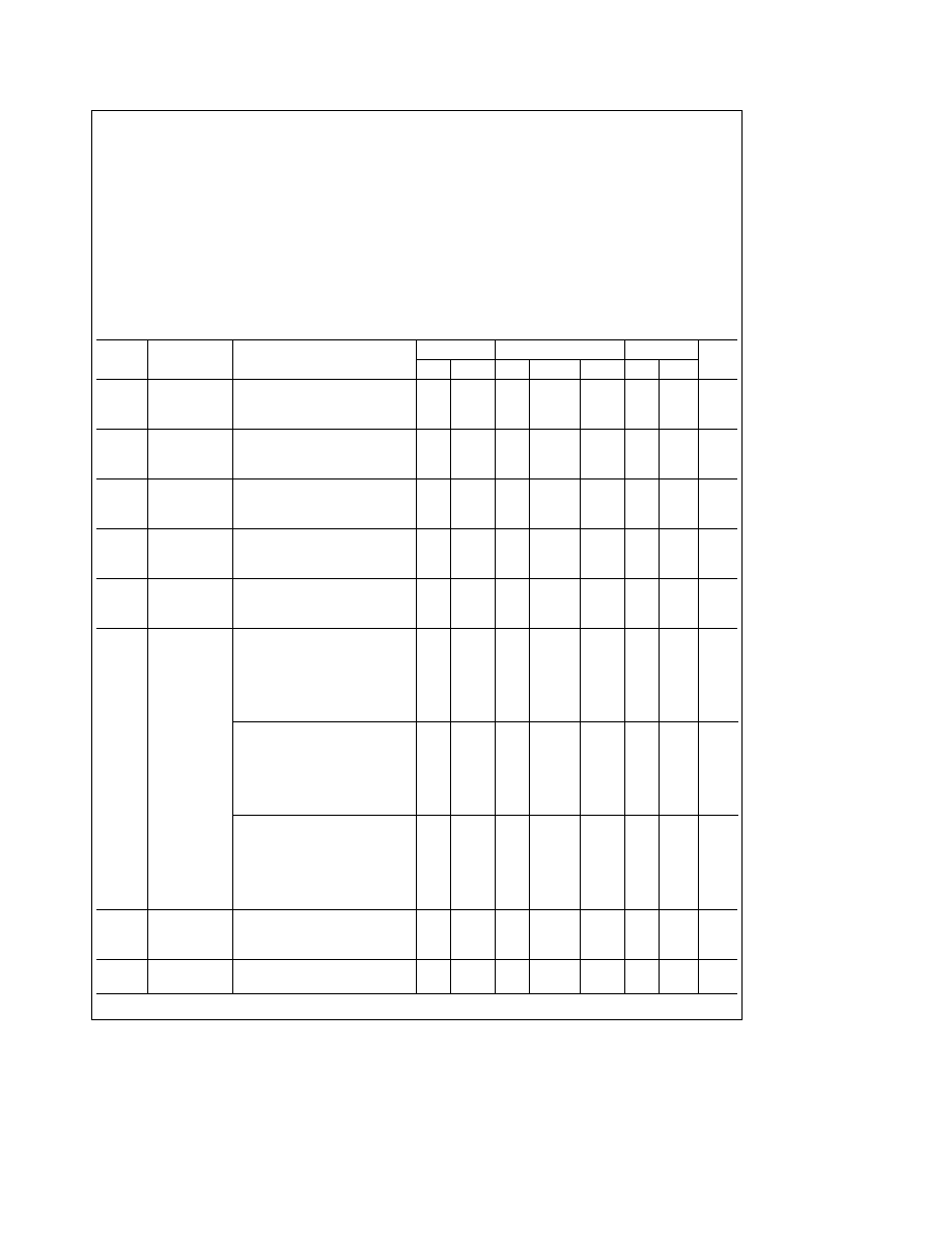
Truth Table
Inputs
Outputs
LE BI LT D C B A a b c d e
f
g Display
X
X
0
X X X X 1 1 1 1 1 1 1
B
X
0
1
X X X X 0 0 0 0 0 0 0
0
1
1
0
0
0
0 1 1 1 1 1 1 0
0
0
1
1
0
0
0
1 0 1 1 0 0 0 0
1
0
1
1
0
0
1
0 1 1 0 1 1 0 1
2
0
1
1
0
0
1
1 1 1 1 1 0 0 1
3
0
1
1
0
1
0
0 0 1 1 0 0 1 1
4
0
1
1
0
1
0
1 1 0 1 1 0 1 1
5
0
1
1
0
1
1
0 0 0 1 1 1 1 1
6
0
1
1
0
1
1
1 1 1 1 0 0 0 0
7
0
1
1
1
0
0
0 1 1 1 1 1 1 1
8
0
1
1
1
0
0
1 1 1 1 0 0 1 1
9
0
1
1
1
0
1
0 0 0 0 0 0 0 0
0
1
1
1
0
1
1 0 0 0 0 0 0 0
0
1
1
1
1
0
0 0 0 0 0 0 0 0
0
1
1
1
1
0
1 0 0 0 0 0 0 0
0
1
1
1
1
1
0 0 0 0 0 0 0 0
0
1
1
1
1
1
1 0 0 0 0 0 0 0
1
1
1
X X X X
*
*
X
e
Don’t Care
*Depends upon the BCD code applied during the 0 to 1 transition of LE.
Display
TL/F/5991 – 2
C1995 National Semiconductor Corporation
RRD-B30M105/Printed in U. S. A.
Absolute Maximum Ratings
(Notes 1 & 2)
If Military/Aerospace specified devices are required,
please contact the National Semiconductor Sales
Office/Distributors for availability and specifications.
DC Supply Voltage (V
DD
)
b
0.5V to
a
18V
Input Voltage (V
IN
)
b
0.5V to V
DD
a
0.5V
Storage Temperature Range (T
S
)
b
65
§
C to
a
150
§
C
Power Dissipation (P
D
)
Dual-In-Line
700 mW
Small Outline
500 mW
Lead Temperature (T
L
)
(Soldering, 10 seconds)
260
§
C
Recommended Operating
Conditions
(Note 2)
DC Supply Voltage (V
DD
)
3V to 15V
Input Voltage (V
IN
)
0V to V
DD
Operating Temperature Range (T
A
)
CD4510BM, CD4516BM
b
55
§
C to
a
125
§
C
CD4510BC, CD4516BC
b
40
§
C to
a
85
§
C
DC Electrical Characteristics
CD4511BM
Symbol
Parameter
Conditions
b
55
§
C
a
25
§
C
a
125
§
C
Units
Min
Max
Min
Typ
Max
Min
Max
I
DD
Quiescent
V
DD
e
5V, V
IN
e
V
DD
or V
SS
5
5
150
m
A
Supply Current
V
DD
e
10V, V
IN
e
V
DD
or V
SS
10
10
300
m
A
V
DD
e
15V, V
IN
e
V
DD
or V
SS
20
20
600
m
A
V
OL
Output Voltage
V
DD
e
5V
0.01
0
0.01
0.05
V
Logical ‘‘0’’
V
DD
e
10V
0.01
0
0.01
0.05
V
Level
V
DD
e
15V
0.01
0
0.01
0.05
V
V
OH
Output Voltage
V
DD
e
5V
4.1
4.1
4.57
4.1
V
Logical ‘‘1’’
V
DD
e
10V
9.1
9.1
9.58
9.1
V
Level
V
DD
e
15V
14.1
14.1
14.59
14.1
V
V
IL
Low Level
V
DD
e
5V, V
OUT
e
3.8V or 0.5V
1.5
2
1.5
1.5
V
Input Voltage
V
DD
e
10V, V
OUT
e
8.8V or 1.0V
3.0
4
3.0
3.0
V
V
DD
e
15V, V
OUT
e
13.8V or 1.5V
4.0
6
4.0
4.0
V
V
IH
High Level
V
DD
e
5V, V
OUT
e
0.5V or 3.8V
3.5
3.5
3
3.5
V
Input Voltage
V
DD
e
10V, V
OUT
e
1.0V or 8.8V
7.0
7.0
6
7.0
V
V
DD
e
15V, V
OUT
e
1.5V or 13.8V
11.0
11.0
9
11.0
V
V
OH
Output
V
DD
e
5V, I
OH
e
0 mA
4.1
4.1
4.57
4.1
V
(Source) Drive
V
DD
e
5V, I
OH
e
5 mA
4.24
V
Voltage
V
DD
e
5V, I
OH
e
10 mA
3.9
3.9
4.12
3.5
V
V
DD
e
5V, I
OH
e
15 mA
3.94
V
V
DD
e
5V, I
OH
e
20 mA
3.4
3.4
3.75
3.0
V
V
DD
e
5V, I
OH
e
25 mA
3.54
V
V
DD
e
10V, I
OH
e
0 mA
9.1
9.1
9.58
9.1
V
V
DD
e
10V, I
OH
e
5 mA
9.26
V
V
DD
e
10V, I
OH
e
10 mA
9.0
9.0
9.17
8.6
V
V
DD
e
10V, I
OH
e
15 mA
9.04
V
V
DD
e
10V, I
OH
e
20 mA
8.6
8.6
8.9
8.2
V
V
DD
e
10V, I
OH
e
25 mA
8.75
V
V
DD
e
15V, I
OH
e
0 mA
14.1
14.1
9.58
14.1
V
V
DD
e
15V, I
OH
e
5 mA
14.27
V
V
DD
e
15V, I
OH
e
10 mA
14.0
14.0
14.17
13.6
V
V
DD
e
15V, I
OH
e
15 mA
14.07
V
V
DD
e
15V, I
OH
e
20 mA
13.6
13.6
13.95
13.2
V
V
DD
e
15V, I
OH
e
25 mA
13.8
V
I
OL
Low Level
V
DD
e
5V, V
OL
e
0.4V
0.64
0.51
0.88
0.36
mA
Output Current
V
DD
e
10V, V
OL
e
0.5V
1.6
1.3
2.25
0.9
mA
V
DD
e
15V, V
OL
e
1.5V
4.2
3.4
8.8
2.4
mA
I
IN
Input Current
V
DD
e
15V, V
IN
e
0V
b
0.10
b
10
b
5
b
0.10
b
1.0
m
A
V
DD
e
15V, V
IN
e
15V
0.10
10
b
5
0.10
1.0
m
A
Note 1:
Devices should not be connected with power on.
2
DC Electrical Characteristics
CD4511BC
Symbol
Parameter
Conditions
b
55
§
C
a
25
§
C
a
85
§
C
Units
Min
Max
Min
Typ
Max
Min
Max
I
DD
Quiescent
V
DD
e
5V
20
20
150
m
A
Supply Current
V
DD
e
10V
40
40
300
m
A
V
DD
e
15V
80
80
600
m
A
V
OL
Output Voltage
V
DD
e
5V
0.01
0
0.01
0.05
V
Logical ‘‘0’’
V
DD
e
10V
0.01
0
0.01
0.05
V
Level
V
DD
e
15V
0.01
0
0.01
0.05
V
V
OH
Output Voltage
V
DD
e
5V
4.1
4.1
4.57
4.1
V
Logical ‘‘1’’
V
DD
e
10V
9.1
9.1
9.58
9.1
V
Level
V
DD
e
15V
14.1
14.1
14.59
14.1
V
V
IL
Low Level
V
DD
e
5V, V
OUT
e
3.8V or 0.5V
1.5
2
1.5
1.5
V
Input Voltage
V
DD
e
10V, V
OUT
e
8.8V or 1.0V
3.0
4
3.0
3.0
V
V
DD
e
15V, V
OUT
e
13.8V or 1.5V
4.0
6
4.0
4.0
V
V
IH
High Level
V
DD
e
5V, V
OUT
e
0.5V or 3.8V
3.5
3.5
3
3.5
V
Input Voltage
V
DD
e
10V, V
OUT
e
1.0V or 8.8V
7.0
7.0
6
7.0
V
V
DD
e
15V, V
OUT
e
1.5V or 13.8V
11.0
11.0
9
11.0
V
V
OH
Output
V
DD
e
5V, I
OH
e
0 mA
4.1
4.1
4.57
4.1
V
(Source) Drive
V
DD
e
5V, I
OH
e
5 mA
4.24
V
Voltage
V
DD
e
5V, I
OH
e
10 mA
3.6
3.6
4.12
3.3
V
V
DD
e
5V, I
OH
e
15 mA
3.94
V
V
DD
e
5V, I
OH
e
20 mA
2.8
2.8
3.75
2.5
V
V
DD
e
5V, I
OH
e
25 mA
3.54
V
V
DD
e
10V, I
OH
e
0 mA
9.1
9.1
9.58
9.1
V
V
DD
e
10V, I
OH
e
5 mA
9.26
V
V
DD
e
10V, I
OH
e
10 mA
8.75
8.75
9.17
8.45
V
V
DD
e
10V, I
OH
e
15 mA
9.04
V
V
DD
e
10V, I
OH
e
20 mA
8.1
8.1
8.9
7.8
V
V
DD
e
10V, I
OH
e
25 mA
8.75
V
V
DD
e
15V, I
OH
e
0 mA
14.1
14.1
14.59
14.1
V
V
DD
e
15V, I
OH
e
5 mA
14.27
V
V
DD
e
15V, I
OH
e
10 mA
13.75
13.75
14.18
13.45
V
V
DD
e
15V, I
OH
e
15 mA
14.07
V
V
DD
e
15V, I
OH
e
20 mA
13.1
13.1
13.95
12.8
V
V
DD
e
15V, I
OH
e
25 mA
13.8
V
I
OL
Low Level
V
DD
e
5V, V
OL
e
0.4V
0.52
0.44
0.88
0.36
mA
Output Current
V
DD
e
10V, V
OL
e
0.5V
1.3
1.1
2.25
0.9
mA
V
DD
e
15V, V
OL
e
1.5V
3.6
3.0
8.8
2.4
mA
I
IN
Input Current
V
DD
e
15V, V
IN
e
0V
b
0.30
b
10
b
5
b
0.30
b
1.0
m
A
V
DD
e
15V, V
IN
e
15V
0.30
10
b
5
0.30
1.0
m
A
3
AC Electrical Characteristics
*
T
A
e
25
§
C and C
L
e
50 pF, typical temperature coefficient for all values of V
DD
e
0.3%/
§
C
Symbol
Parameter
Conditions
CD4511BX
Units
Min
Typ
Max
C
IN
Input Capacitance
V
IN
e
0
5.0
7.5
pF
t
r
Output Rise Time
V
DD
e
5V
40
80
ns
(Figure 1a)
V
DD
e
10V
30
60
ns
V
DD
e
15V
25
50
ns
t
f
Output Fall Time
V
DD
e
5V
125
250
ns
(Figure 1a)
V
DD
e
10V
75
150
ns
V
DD
e
15V
65
130
ns
t
PLH
Turn-Off Delay Time
V
DD
e
5V
640
1280
ns
(Data)
(Figure 1a)
V
DD
e
10V
250
500
ns
V
DD
e
15V
175
350
ns
t
PHL
Turn-On Delay Time
V
DD
e
5V
720
1440
ns
(Data)
(Figure 1a)
V
DD
e
10V
290
580
ns
V
DD
e
15V
195
400
ns
t
PLH
Turn-Off Delay Time
V
DD
e
5V
320
640
ns
(Blank)
(Figure 1a)
V
DD
e
10V
130
260
ns
V
DD
e
15V
100
200
ns
t
PHL
Turn-On Delay Time
V
DD
e
5V
485
970
ns
(Blank)
(Figure 1a)
V
DD
e
10V
200
400
ns
V
DD
e
15V
160
320
ns
t
PLH
Turn-Off Delay Time
V
DD
e
5V
313
625
ns
(Lamp Test)
(Figure 1a)
V
DD
e
10V
125
250
ns
V
DD
e
15V
90
180
ns
t
PHL
Turn-On Delay Time
V
DD
e
5V
313
625
ns
(Lamp Test)
(Figure 1a)
V
DD
e
10V
125
250
ns
V
DD
e
15V
90
180
ns
t
SETUP
Setup Time
V
DD
e
5V
180
90
ns
(Figure 1b)
V
DD
e
10V
76
38
ns
V
DD
e
15V
40
20
ns
t
HOLD
Hold Time
V
DD
e
5V
0
b
90
ns
(Figure 1b)
V
DD
e
10V
0
b
38
ns
V
DD
e
15V
0
b
20
ns
PW
LE
Minimum Latch Enable
V
DD
e
5V
520
260
ns
Pulse Width
(Figure 1c)
V
DD
e
10V
220
110
ns
V
DD
e
15V
130
65
ns
*AC Parameters are guaranteed by DC correlated testing.
4
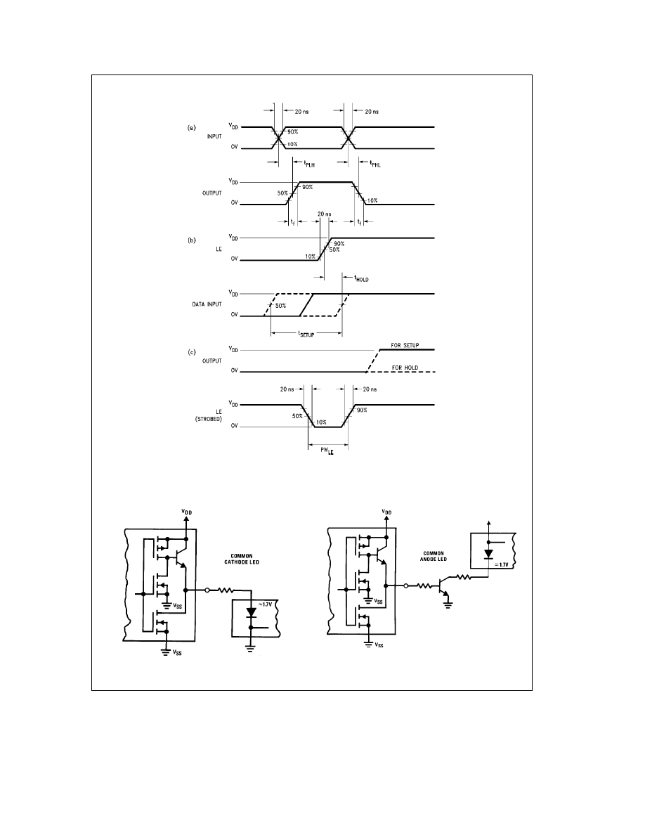
Switching Time Waveforms
TL/F/5991 – 4
FIGURE 1
Typical Applications
Light Emitting Diode (LED) Readout
TL/F/5991 – 5
TL/F/5991 – 6
5
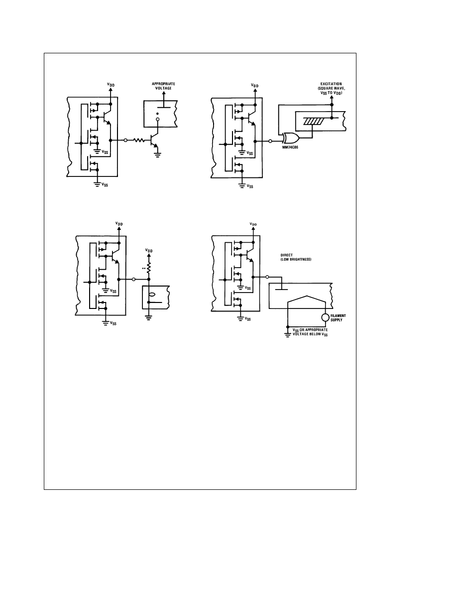
Typical Applications
(Continued)
Gas Discharge Readout
TL/F/5991 – 7
Liquid Crystal (LC) Readout
TL/F/5991 – 8
Direct DC drive of LC’s not recommended for life of LC readouts.
Incandescent Readout
TL/F/5991 – 9
**A filament pre-warm resistor is recommended to
reduce filament thermal shock and increase the ef-
fective cold resistance of the filament.
Fluorescent Readout
TL/F/5991 – 10
6
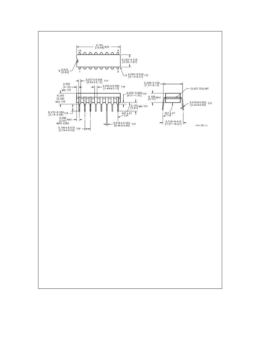
Physical Dimensions
inches (millimeters)
Ceramic Dual-In-Line Package (J)
Order Number CD4511BMJ or CD4511BCJ
NS Package Number J16A
7
CD4511BM/CD4511BC
BCD-to-7
Segment
Latch/Decoder/Driver
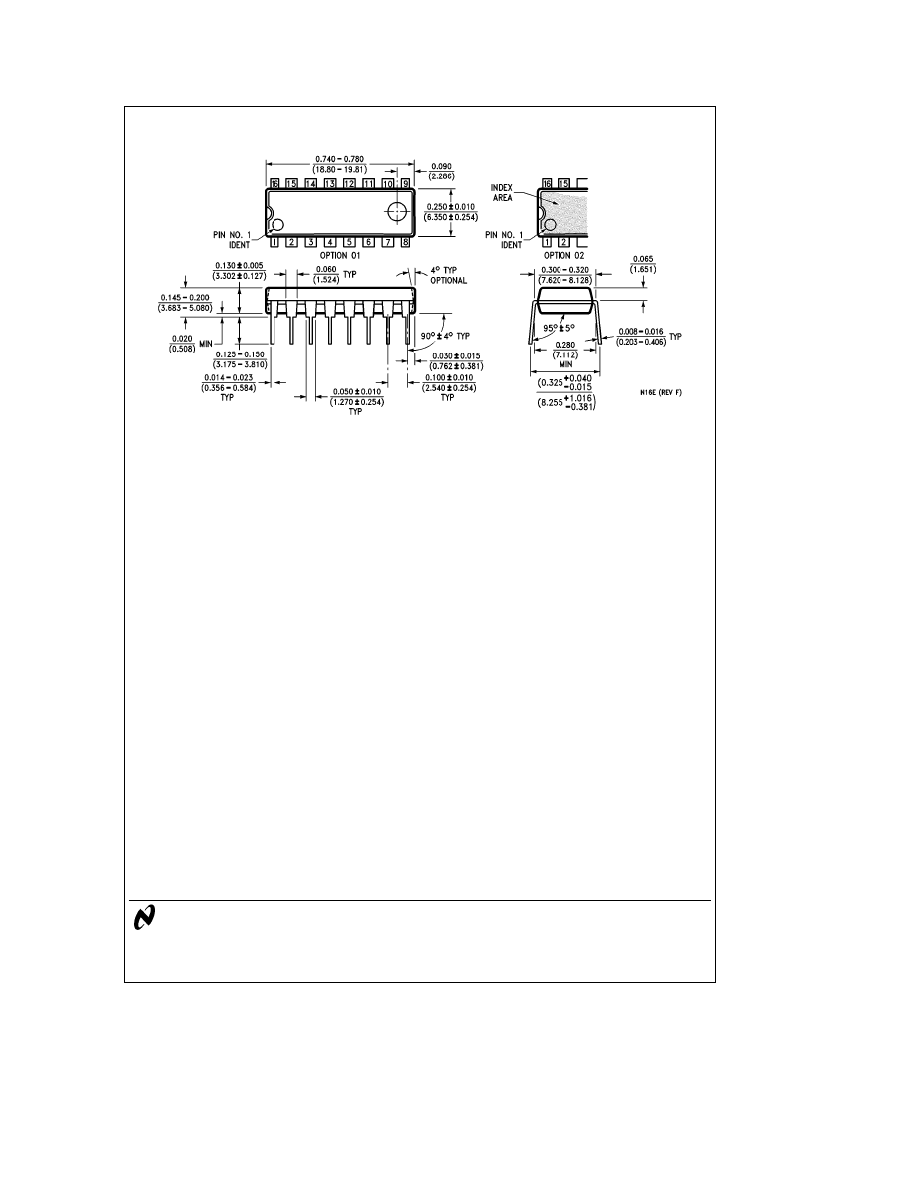
Physical Dimensions
inches (millimeters) (Continued)
Molded Dual-In-Line Package (N)
Order Number CD4511BMN or CD4511BCN
NS Package Number N16E
LIFE SUPPORT POLICY
NATIONAL’S PRODUCTS ARE NOT AUTHORIZED FOR USE AS CRITICAL COMPONENTS IN LIFE SUPPORT
DEVICES OR SYSTEMS WITHOUT THE EXPRESS WRITTEN APPROVAL OF THE PRESIDENT OF NATIONAL
SEMICONDUCTOR CORPORATION. As used herein:
1. Life support devices or systems are devices or
2. A critical component is any component of a life
systems which, (a) are intended for surgical implant
support device or system whose failure to perform can
into the body, or (b) support or sustain life, and whose
be reasonably expected to cause the failure of the life
failure to perform, when properly used in accordance
support device or system, or to affect its safety or
with instructions for use provided in the labeling, can
effectiveness.
be reasonably expected to result in a significant injury
to the user.
National Semiconductor
National Semiconductor
National Semiconductor
National Semiconductor
Corporation
Europe
Hong Kong Ltd.
Japan Ltd.
1111 West Bardin Road
Fax: (a49) 0-180-530 85 86
13th Floor, Straight Block,
Tel: 81-043-299-2309
Arlington, TX 76017
Email: cnjwge
@
tevm2.nsc.com
Ocean Centre, 5 Canton Rd.
Fax: 81-043-299-2408
Tel: 1(800) 272-9959
Deutsch Tel: (a49) 0-180-530 85 85
Tsimshatsui, Kowloon
Fax: 1(800) 737-7018
English
Tel: (a49) 0-180-532 78 32
Hong Kong
Fran
3ais Tel: (a49) 0-180-532 93 58
Tel: (852) 2737-1600
Italiano
Tel: (a49) 0-180-534 16 80
Fax: (852) 2736-9960
National does not assume any responsibility for use of any circuitry described, no circuit patent licenses are implied and National reserves the right at any time without notice to change said circuitry and specifications.
Wyszukiwarka
Podobne podstrony:
4511
4511
4511
4511
4511
4511
MTA 4511 12
praca-licencjacka-b7-4511, Dokumenty(8)
MTAA 4511 12V
4511
MAXDATA NB ECO 4511 IW dataSheet ESES(1)
4511 ac
MAXDATA NB ECO 4511 IW dataSheet ITIT
a lot of various circuits index 1128613 25 4511
więcej podobnych podstron