
1
MEMS Technology for Optical Crosslink for Micro/Nano Satellites
W. Piyawattanametha, L. Fan
∗
, S. S. Lee, John G. D. Su and M. C. Wu
Department of Electrical Engineering, University of California, Los Angles
66-147D Engineering IV, 405 Hilgard Ave., Los Angeles CA 90095-1594, USA
Tel: 310-825-7338, Fax: 310-794-5513, Email:
wu@ee.ucla.edu
∗
Optical Micro-Machines, Inc., 6160 Lusk Blvd., Suite C-105, San Diego, CA 92121, USA
Abstract
We report on a novel, compact two-
dimensional (2D) scanning micromirror for
free space optical crosslinks for micro and
nano satellites. Using a novel
micromachined structure called Micro-
Elevator by Self-Assembly (MESA) [1], the
micromirror is suspended above the
substrate by several hundred micrometers.
Large mirror size and wide scanning range
are achieved simultaneously. Large number
of resolvable spots (>100) can be realized.
Experimentally, optical scanning angles of
±
14
°
have been achieved for the 2D scanner
with mirror size of 400
µ
m
×
400
µ
m. The
resonant frequencies are around 500 Hz.
Introduction
Free-space optical
crosslinks offers
unprecedented connectivity and link
capacity for communication among
satellites. Pointing and tracking (P/T) of the
optical beams are one of the most
challenging tasks for this application.
Conventional systems employ motorized
gimbles, which are bulky, heavy, and
expensive. The Micro-Electro-Mechanical-
Systems (MEMS) technology offers a
revolutionary approach to implement
compact and light weight P/T systems for
micro and nano satellites. Two-dimensional
(2D) optical scanners with large rotation
angles, narrow beam divergence, and high
resonant frequency are the key components
for the P/T systems.
Two-dimensional optical scanner can be
realized by combining two one-dimensional
(1D) scanners with orthogonal axes or using
a single micromirror with two degrees of
freedom. Several surface-micromachined
1D scanners have been reported [2-4]. The
combinations of two cascaded 1D scanners
have been demonstrated by M. H. Kiang, et
al. [4] and P. Hagelin, et al. [5]. However,
the cascaded 1D scanners have several
disadvantages. The optical beams moves
across the second mirror as the first mirror
scans. As a result, either a large second
mirror or some imaging optics is needed for
large scan angles. The former results in low
resonant frequency, while the latter makes it
more difficult to monolithically integrate the
2D scanners. The 2D scanner using a single
mirror with two degrees of freedom are
therefore more desirable. Previously,
several 2D Scanners have been reported
[6,7]. To achieve a large number of
resolvable spots for the 2D scanner, large
separation between the micromirror and the
substrate is required. This can be achieved
by etching the substrate [6] or wafer
bonding technique [7]. Though standard
surface-micromachining offers many
advantages and flexibility, most of the 2D
scanners to date can only achieve a very
limited number of resolvable spots.
In this paper, we report a novel surface-
micromachined 2D optical scanning
micromirror fabricated by the standard
surface-micromaching process offered by
MCNC [8]. This micromirror has a large
mirror size, large scanning angles, and small
actuation voltage. It is based on the MESA
structure, which allows large micromirrors
to be suspended at several hundreds
micrometers above the substrate. The
micromirror has an area of 400
µ
m
×
400
µ
m.
2
Design and Fabrication
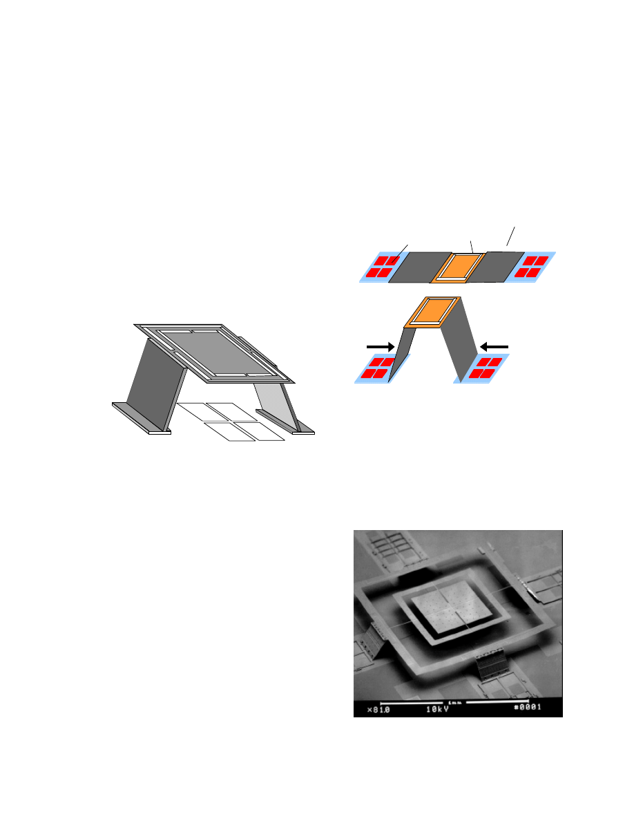
The schematic drawing of the 2D optical
scanning micromirror is illustrated in Fig. 1.
A nested torsion mirror is attached to a fixed
polysilicon frame supported by the MESA
structure. The MESA consists of five
hinged polysilicon plates. The two outer
plates are connected to in-plane micro
actuators. As the microactuators move
towards each other, the center plate will
buckle up and rise above the surface of the
substrate. The height is defined by the
length of the side support plates, and can be
made as high as several millimeters.
Torsion mirrors as large as 5 mm x 5 mm
have been successfully suspended by the
MESA structure.
I
II
III
IV
Bo tto m E le ctrod e s
Figure 1: Schematic of 2D scanning
micromirror realized by MESA.
The micromirror is attached to a pair of
suspended frames through two sets of
orthogonal torsion beams. The micromirror
can be rotated around two axes by applying
electrostatic force between the mirror and
the quadrant electrodes on the substrate.
The self-assembly and operation of the
micromirror is illustrated in
Fig. 2. For simple illustration, only two side
support plates are drawn. The basic
structure consists of three parts: the
micromirror platform, the side support
plates, and scratch drive actuator (SDA)
arrays [9]. The plates are joined together by
polarity hinges. These hinges join two
polysilicon plates together and allow them to
bend only in one direction (either upwards
or downwards). Details of the polarity
hinges have been described in [1]. The 2D
scanner can be fully assembled by applying
electrical bias to the SDA arrays [9] attached
to the outer plates. The side support plates
with polarity hinges effectively translate the
in-plane motion into out-of-plane motion,
which in turn raise the platform, as
illustrated in Fig. 2 (b).
Micromirror
Platform
X-axis
Actuators
SideSupport
Plate
(a)
(b)
Figure 2 : Schematic diagrams illustrating the
principle of the self-assembled
micromirror (a) before assembly,
(b) micromirror after assembly.
Figure 3 shows the scanning electron
micrograph (SEM) of the 2D scanner. To
improve the stability of the fixed frame, the
MESA is supported from four sides.
Figure 3: SEM of the 2D scanner.
3
Electrical Biasing and
Controlling Scheme
The micromirror (400
µ
m x 400
µ
m) is
attached to the fixed frame by torsion beams
and suspended over four electrodes. The
height of the structure is set to be 72
µ
m
above the electrodes. The torsion beams are
2
µ
m and 3
µ
m wide for the inner and the
outer frames, respectively, 200
µ
m long, and
1.5
µ
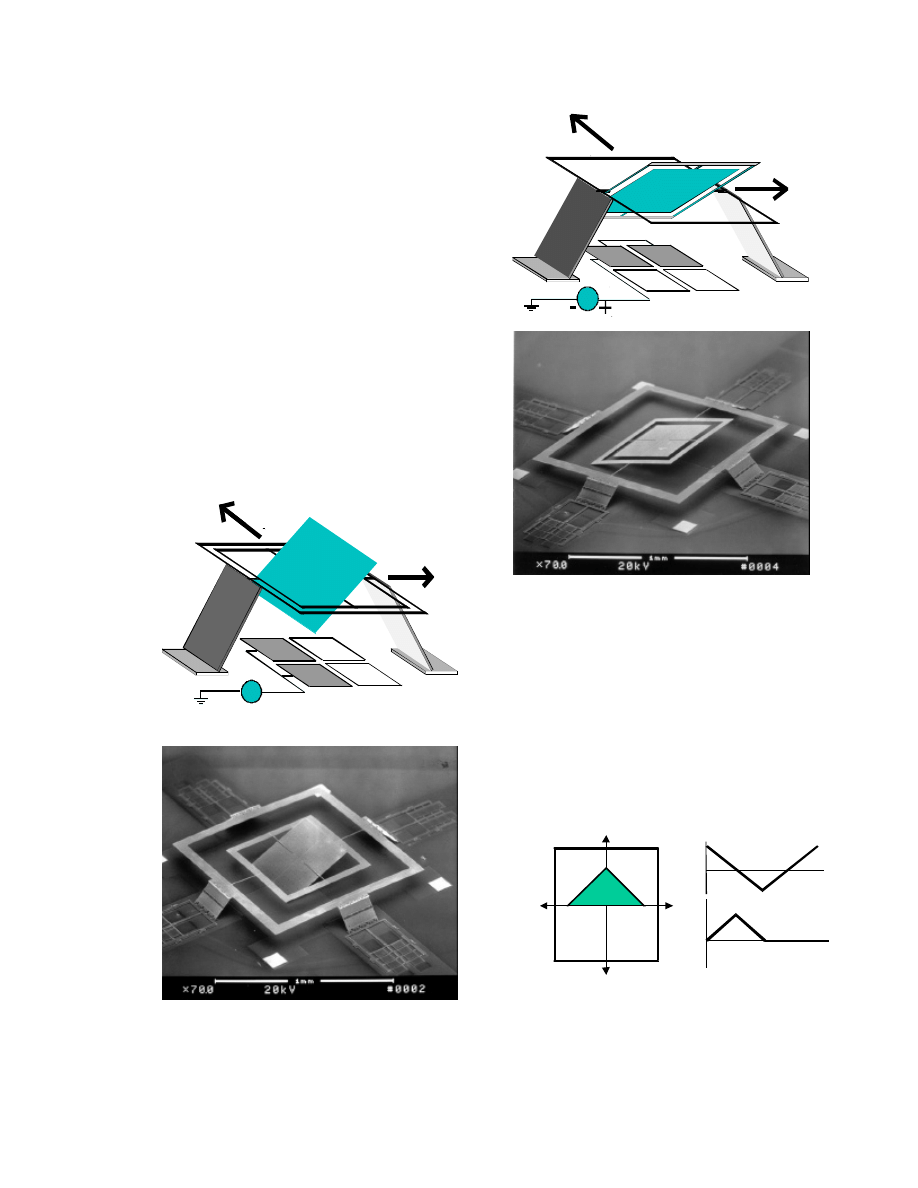
m thick. The 2D scanner is biased
electrostatically by the quad-electrodes in
the analog regime before snap-down. By
applying voltage bias to electrode I and II,
the mirror is rotated around the Y-axis (Fig.
5 (a)). The mirror is rotated around X-axis
when applying electrical bias to electrode II
and III (Fig. 5 (b)).
II
III
IV
I
Y
X
+
-
Figure 5 (a) : The mirror is rotated around the Y-
axis.
II
III
IV
I
X
Y
Figure 5 (b) : The mirror is rotated around the X
axis.
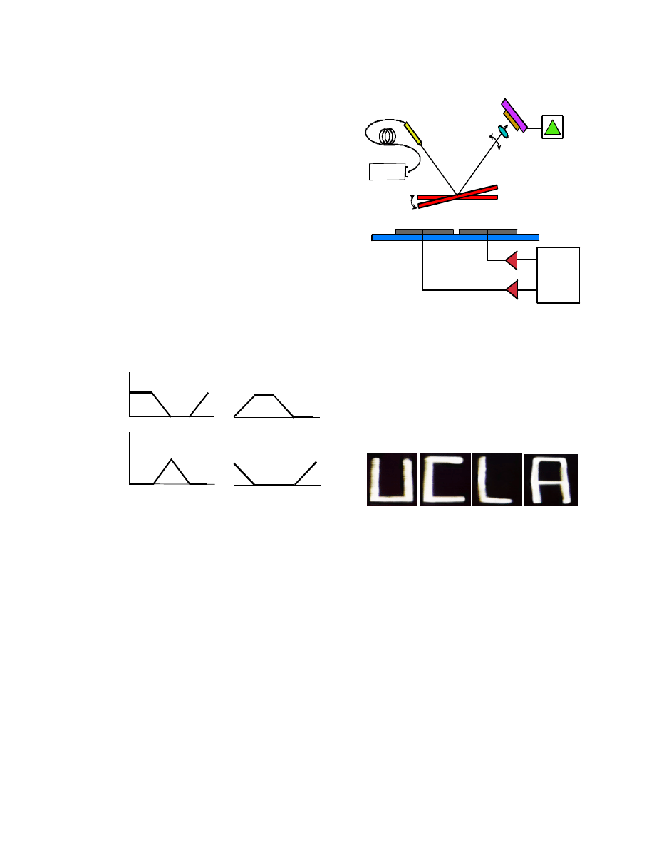
For two-dimensional scanning, we divide
the scanning pattern into four quadrants: Q1,
Q2, Q3 and Q4. Fig. 6 (a) illustrates a
triangle scanning pattern. It starts from
point 1 to point 2, point 2 to point 3, and
finally back to point 1 again. The variation
of the mirror angles,
θ
x and
θ
y, versus time
is illustrated in Fig. 6 (b).
θ
Y
θ
y
2
I
III
IV
3
1
II
θ
x
-
θ
y
-
θ
x
2
3
1
θ
X
1
time
time
(a) (b)
Figure 6 : (a) Triangle scanning pattern.
(b) Variation of the mirror angles,
θ
x
and
θ
y, versus time .
4
When the mirror scans from point 1 to point
2,
θ
x reduced from a positive value to zero
while
θ
y increased from zero to a positive
value. Scanning from point 2 to point 3 and
point 3 to point 1 can be realized by the
same principle.
The mirror angles can be controlled by
properly biasing the quad electrodes.
Applying a voltage bias on electrode I will
tilt the mirror in the +
θ
x and +
θ
y direction,
Q1. Similarly, biasing electrode II, III, and
IV will tilt the mirror in Q2, Q3, and Q4,
respectively. Arbitrary scanning pattern is
obtained by supplying proper waveforms to
the quad electrodes. We use a computer
controlled programmable waveform
generator to supply the biases for all the
electrodes. Fig. 7 shows the biasing
waveforms for scanning a triangle pattern.
1
1
2
3
1
2
3
1
1
2
3
1
1
2
3
1
V
I
V
III
time
time
time
time
V
II
V
IV
Figure 7 : Waveform patterns for each electrode.
The experimental setup for testing the 2D
scanner is shown in Fig. 8. The system is
composed of a 0.8 mW He-Ne laser
operating, a fiber optic collimator, an
imaging lens, a CCD camera, and a
computer-controlled arbitrary waveform
generator (National Instruments arbitrary
waveform generators card AT-AO-10).
The He-Ne laser is used as the light source
for this scanning system. The collimated
light from the fiber collimator is projected
directly onto the micromirror. The reflected
beam from the micromirror is collected by
the imaging lens before it falls on the CCD
camera.
CCD
Camera
Display
System
Fiber Lens
Imaging
lens
BottomElectrodes
ScanningMirror
633nm
He-Ne Laser
Computer
Controlled
Waveform
Generators
Figure 8 : Experimental setup of the
scanning system.
Data from the experiment suggests that the
spot size does not change appreciably as the
mirror rotates. Displayed in Fig. 9 are four
individual characters (UCLA) written by
this laser scanning system to demonstrate
the 2D scanning ability.
Figure 9 : Four characters (UCLA) displayed
individually by the laser scanning
system shown in Figure 8.
Mathematical Modeling
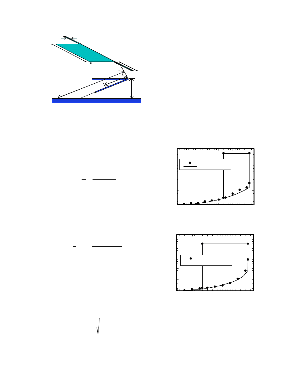
The structural parameter dependence of the
yielding voltage was investigated by
modeling the electrostatic torque on the
mirror, as shown in Fig. 10 [10]. Two
assumptions are made to simplify the
calculation: 1) The distribution of the
electrostatic field is uniform along the
torsion beams, 2) The shape of the field is
represented by the arc whose pivot is at the
intersection, B, of the virtually extended
mirror and the counter electrode.
5
Figure 10 : Analytical model of the
electrostatic torsion mirror.
When the mirror (W: width, L: length) is
rotated inward by an angle
θ,
the length of
BO is R=d/sin(
θ),
where d is equal to the
height of micromirror structure. Since the
length of the arc at x on the mirror is
calculated a = d – xsin(
θ),
the magnitude of
electrostatic field at x is
θ
sin
x
d
V
d
V
E
−
=
=
, (1)
where V is the applied voltage. The
electrostatic pressure on the surface is
P=
ε
E
2
/2, where
ε=8.85
x10
-12
F/m is the
dielectric constant of the vacuum. By
integrating the electrostatic torque xPWdx
over the electrode, we obtain the total
torque by exerted electrostatic attraction
∫
−
=
L
e
dx
x
d
x
W
V
T
0
2
2
)
sin
(
2
θ
ε
. (2)
On the other hand, the restoring torque of
the torsion beams is
−
×
=
t
w
w
t
l
Gwt
T
m
2
tanh
192
1
3
2
5
3
π
π
θ
,(3)
where G is the elastic constant of
polysilicon. The resonant frequency of the
torsion mirror is [11]
Ml
Gwt
r
F
r
6
2
1
4
π
=
. (4)
Experimental Results
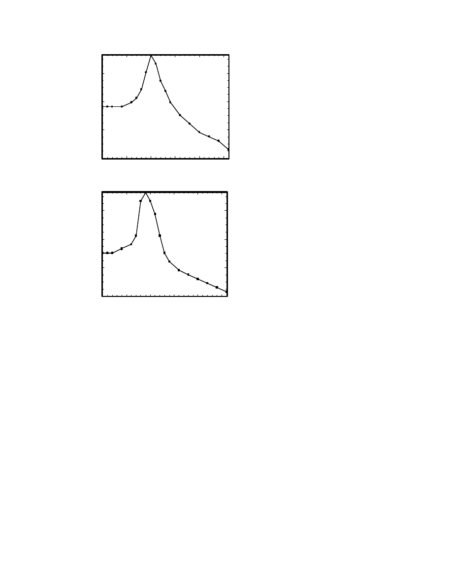
From the experiment, we find the pull-in
voltage and the resonant frequency of the
outer and inner frames to be 104.8 V, 552
Hz and 94.5 V, 448 Hz, respectively. The
optical deflection angle versus the applied
voltage of the outer and the inner frames are
illustrated in Fig. 11 (a) and (b),
respectively. The measured data agrees well
with the theoretically calculated data using
72 GPa for the elastic constant of
polysilicon and setting the widths of the
outer and inner frames to 2.95
µ
m and 1.9
µ
m respectively. However, the calculated
angle at pull-in voltage is smaller than the
experimental values. Fig. 12 (a) and (b) are
the measured frequency responses.
0
5
10
15
20
0
20
40
60
80
100
Experimental Result
Theoretical Result
Applied Voltage (V)
O
p
ti
c
a
l
D
e
fl
e
c
ti
o
n
A
n
g
le
(
°
)
(a)
0
5
10
15
20
25
0
20
40
60
80
100
Experimental Result
Theoretical Result
Applied Voltage (V)
O
p
ti
c
a
l
D
e
fl
e
c
ti
o
n
A
n
g
le
(
°
)
(b)
Figure 11 : (a) Optical Angle under applied
voltage for outer frame.
(b) Optical angle under applied
voltage for inner frame.
A
θ
O
B
x
d
R
w
W
L
l
t : thickness
6
0
20
40
60
0
250
500
750
1000
1250
Frequency (Hz)
D
is
p
la
c
e
m
e
n
t
(
µ
m
)
(a)
0
20
40
60
0
250
500
750
1000
1250
Frequency (Hz)
D
is
p
la
c
e
m
e
n
t
(
µ
m
)
(b)
Figure 12 : (a) Frequency Response of the outer
frame.
(b) Frequency Response of the inner
frame.
The micromirror in this scanning system
exhibit some curvature, resulting from stress
gradients in the polysilicon film.
Differences in curvature were found
between identical devices on the same chip.
Such anomalies are likely due to variations
in the fabrication process.
Conclusion
We have demonstrated a novel self-
assembled two-dimensional scanning
micromirror using standard surface
micromachining technology. Large optical
deflection angles (
±
14 degrees for the inner
frame and
±
7 degrees for the outer frame)
have been achieved for a 400
µ
m x 400
µ
m
micromirror. The applications of this device
include display, printing, optical data
storage, optical scanning microscopes, and
free-space optical links between satellites.
Acknowledgements
The author would like to thank Richard
Chen, Thomas Jung, Andrew Rollinger, Sagi
Mathai, and Hung Nguyen for technical
assistance. This project is supported in part
by DARPA.
Reference :
1. Li Fan, M. C. Wu, Kent D. Choquette,
and Mary H. Crawford, “Self-assembled
Microactuated XYZ Stages for Optical
Scanning and Alignment,” Proceedings
of International Solid State Sensors and
Actuators Conference (Transducers’97),
Chicago, IL, USA, June 16-19, 1997, P.
319-322
2. S. S. Lee, and M. C. Wu, “Surface-
Micromachined Vertical Torsion Mirror
Switches,” International Conference on
Optical MEMS and their Applications
(MOEMS’97), Nara, Japan, November
18-21, 1997, P. 85-88
3. G. D. Su, S. S. Lee, and M. C. Wu, “
Out-of-Plane Vertical Torsion Mirror
for Optical Scanner and Chopper
Application,” Conference on Lasers and
Electro-Optics (CLEO’98), San
Francisco, California, May 3-8, 1998 P.
479-480
4. M. H. Kiang, D. A. Francis, C. J.
Chang-Hasnain, O. Solgaard, and K. Y.
Lau, “Actuated Polysilicon
Micromirrors for Raster-Scanning
Displays,” Proceedings of International
Solid State Sensors and Actuators
Conference (Tranducers’97), Chicago,
IL, USA, June 16-19, 1997, P. 323-326
5. P. Hagelin, K. Cornett, and O. Solgaard,
“Micromachined Mirrors in a Raster
Scanning Display,” IEEE/LEOS

7
Summer Topical Meeting, Monterey,
California, July 20-24, 1998, P. 109-110
6. V. R.
Dhuler, M. Walters, R.
Mahadevan, A. B. Cowen, and K. W.
Markus, “A Novel Two Axis Actuator
for High Speed Large Angular
Rotation,” Proceedings of International
Solid State Sensors and Actuators
Conference (Tranducers’97), Chicago,
IL, USA, June 16-19, 1997, P.327-330
7. W. Dotzel, T. Gessner, R. Hahn, C.
Kaufmann, K. Kehr, S. Kurth, and J.
Mehner, “Silicon Mirrors and
Micromirror Arrays for Spatial Laser
Beam Modulation,” Proceedings of
International Solid State Sensors and
Actuators Conference (Transducers’97),
Chicago, IL, USA, June 16-19, 1997, P.
81-84
8. MEMS Technology Applications Center
at Microelectronics Center at North
Carolina (MCNC), Research Triangle
Park, North Carolina
9. A. Terunobu and H. Fujita, “ A
Quantitative Analysis of Scratch Drive
Actuator Using Buckling Motion,”
Proceedings of IEEE Micro Electro
Mechanical Systems, 1995, P. 310-315
10. H.
Toshiyoshi, and H. Fujita,
“Electrostatic micro-torsion Mirrors for
an Optical Switch Matrix,” Journal of
Micro Electro Mechanical Systems, Vol.
5, No. 4, December 1996, P. 231-237
11. E. Hashimoto, Y. Uenishi, K. Honma,
and S. Ngaoka, “ Micro-optical gate for
fiber optic communication,”
Proceedings of International Solid State
Sensors and Actuators Conference
(Transducers’97), Chicago, IL, USA,
June 16-19, 1997, P. 331-334
Wyszukiwarka
Podobne podstrony:
New technologies for cervical cancer screening
Minor data package v 7 05 (MCU SW 4 03 38) only for Field Test variant phones
New hybrid drying technologies for heat sensitive foodstuff (S K Chou and K J Chua)
Installation technology for Foundation Fieldbus
Coupling of Technologies for Concurrent ECD and Barite Sag Management
New technologies for cervical cancer screening
Coupling of Technologies for Concurrent ECD and Barite Sag Management
13 IMPROVING ELECTROSTATIC ACTUATORS for micro mirrors
GATE Solar Drying Technology for Food Preservation
Kat Simpson [Devils 03 & 04] Hell for the Holidays 2
Kat Simpson [Devils 03 & 04] Hell for the Holidays 1
03 Humanism Forerunner For Antichrist
2002 03 Exporing Korganizer for Scheduling Appointments and Tasks
Scarlet Hyacinth Spirit Wolves 03 Two Mates for a Magistrate
Kat Simpson [Devils 03 & 04] Hell for the Holidays 3
więcej podobnych podstron