Using the Siemens S65 – Display
by
Christian Kranz
, October 2005
(
http://www.superkranz.de/christian/S65_Display/DisplayIndex.html
)
( PDF by Benjamin Metz, September 09
th
, 2006 )
About the Display:
Siemens used for the mobile phones S65, M65, CX65 and SK65 a 16-bit color TFT
display with 132x176 pixel. This display has integrated white backlight LED's and an
attractive screen size.
The display is available for less than 20 EUR in phone part shops and ebay.
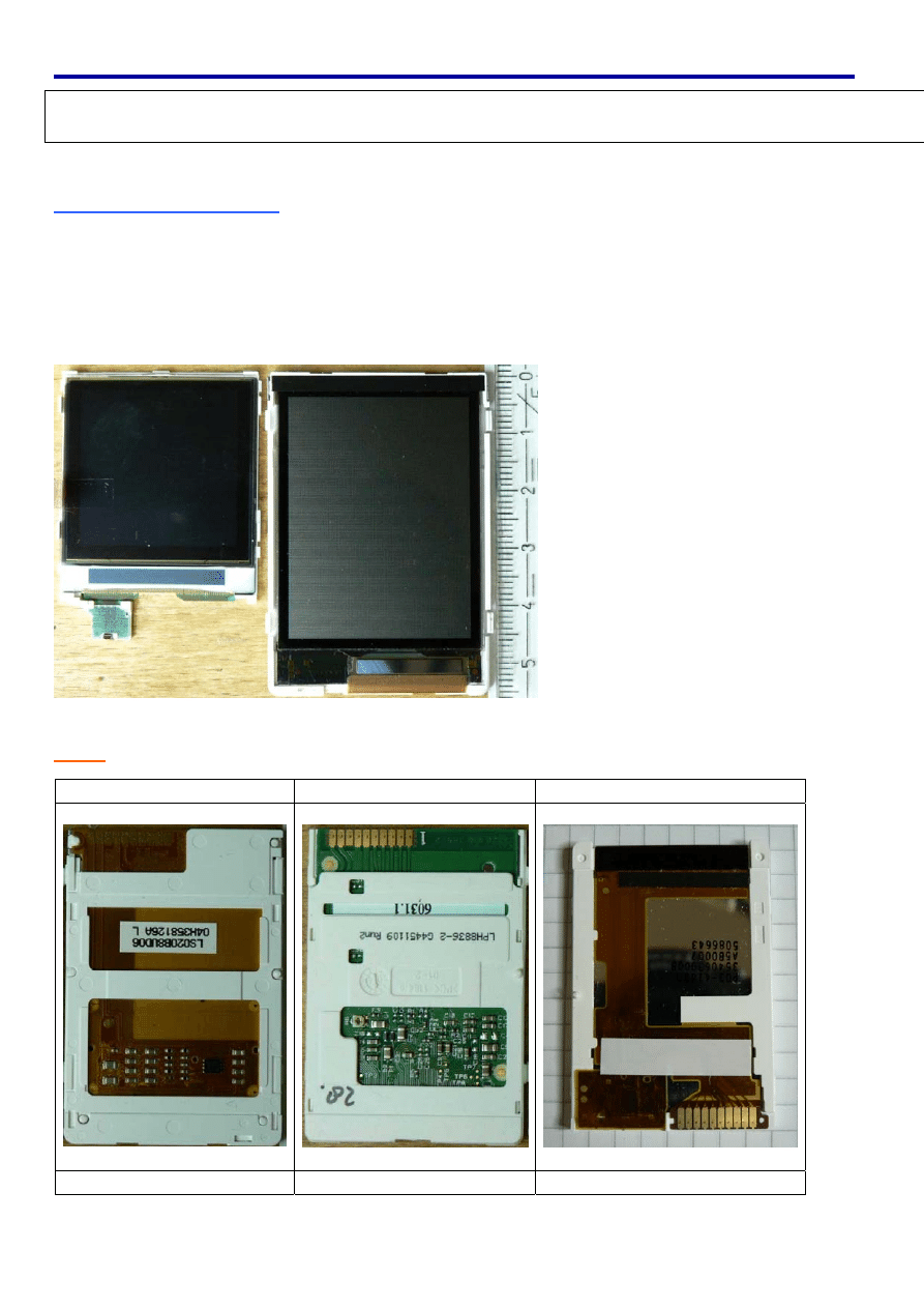
The following picture compares the well known Nokia 6100 display with the
S65 - display.
Info:
Currently there are three different display types known.
LS020…… LPH88…… L2F50……
Sharp
Hitachi HD66773
Epson L2F50..
1
Dimension:
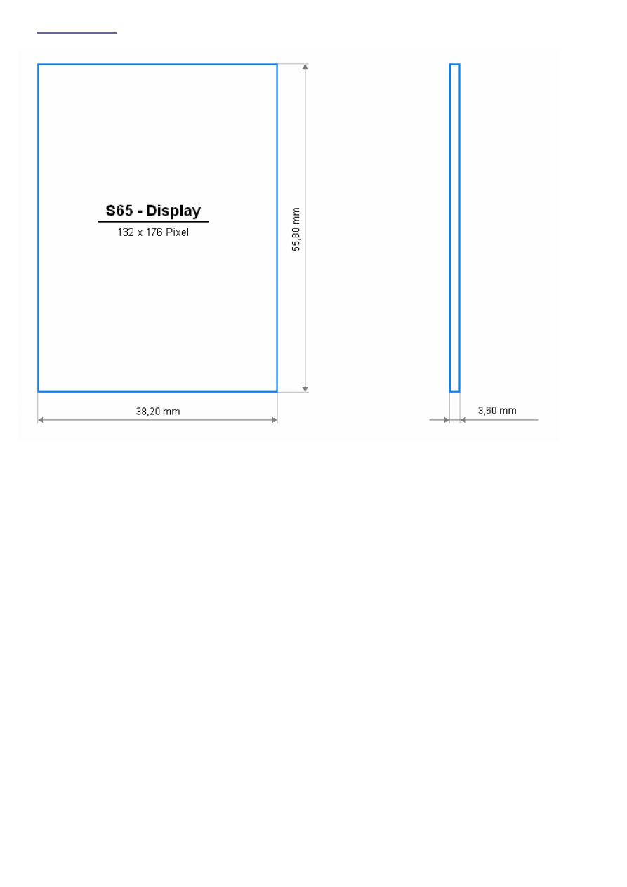
The picture below shows the dimensions of the display.
The following pages describe how to use this display in own applications. Actually it is
focused on the ATMEL
®
AVR processor but from the description
it should be possible to use it with other controller also.
2
Hardware:
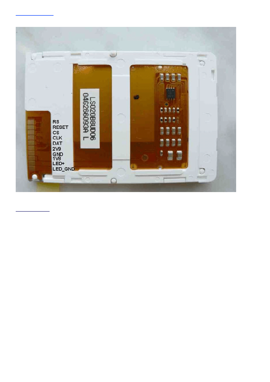
The Display pin description can be found on this Picture:
Schematic:
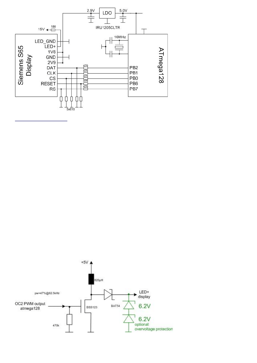
The schematic of the testboard is shown in the picture below. Both display supplies are
connected to a 2.9V supply that is generated out of an LDO from the 5.0V supply of the
ATMEL
®
AVR µC. I used the IRU1205CLTR LDO because I will later need the power
on/off feature of this LDO. The ATMEL
®
AVR µC is running with 16MHz.
The five interface lines between the display and the µC are level-shifted from the 5V
domain of the µC to the 2.9V domain of the display. Because the interface will run with
8MHz the impedance has to be low to get stable signals. It might be a good idea to go
to active level shifter in future to save power, especially for the RESET line because this
line has to be high as long as the display is used. On the other hand you can use a
higher impedance level shifter here because speed is not important.
3
Display Backlight:
The display forward voltage was measured at one part to be 10.4V at 20mA current.
That means a relative large voltage is needed. This voltage can be easily generated
with a PWM signal generator of the µC. (Do not forget to switch on the current
limitation of your power supply until the PWM generator is running correct. If you drive
the n-channel gate high for a longer time you will have a short circuit.) For the circuit
below you need a pulse width (high/period) of 47% at a period frequency of 62.5kHz to
generate the required voltage with 15mA LED current. A block capacitor is already
implemented on the display and is not needed. You can adjust the brightness of the
display by varying the OCRn value. No software interaction is needed to generate this
waveform with AVR processor. The code example below for the ATmega128 uses timer
2 with OC2 (PB7) for PWM generation. That means you can not use PB7 for LCD_RS
any more (as in the circuit above). LCD_RS can be changed to PB5 for example.
For the final running application an over voltage protection is not required. But during
testing and development it is not a bad idea to add a protection device. That might
protect the circuit against hardware/software malfunctions.
PWM Programming example ATmega128 (AVR)
// backlight PWM generation
// use timer 2 in fast PWM mode for this
PORTB &= ~_BV(PB7); // clear port before enable
DDRB |= _BV(PB7); // will be used for OC2, must be output
TCCR2 = _BV(WGM21) | _BV(WGM20) | _BV(COM21) | _BV(CS20);
TCNT2=0x00;
OCR2=120
4

5
I) LS020 - Display:
Software - (Commands and Data):
Data and commands to the display controller are distinguished by the RS line. If RS is
high, the controller expects commands, if the RS line is low it expects data.
RS = high Command
RS = low Data
Initialization Commands:
A LCD TFT display is programmed in three steps. To switch on the display a initialization
sequence is needed to program the power chip of the display.
That is needed because of the high multiplex rate of the display a relative high voltage
is used for driving the glass. The glass voltage can be in the 10V to 20V range and is
usually generated by charge pumps.
After switching on the power usually the display parameter are programmed.
In some cases also the boost circuit has to be reprogrammed from startup to active.
After startup the display can be used for displaying...
The originally measured seven initialization sequences from the S65 display can luckily
be reduced to three sequences. In addition we do not need the very long time intervals
Siemens used in here approach. The first (of the three) used initialization sequence is:
INIT1: (Display Software Reset)
0xFDFD,
0xFDFD
It looks like this sequence starts the display controller. After a certain time
(min. 50ms) the second init command sequence is transmitted to the display.
INIT2:
0xEF00
0xEE04,
0x1B04
0xFEFE,
0xFEFE
0xEF90, 0x4A04, 0x7F3F, 0xEE04, 0x4306
After that we need to wait for the display internal voltage settling.
This wait time is very sensitive. If the time is too short or too long the display will
not work! It was measured to be 7ms and this value shall also be used to drive the
display with the sequences shown here.

6
The third sequence follows directly and is:
INIT3:
0xEF90, 0x0983, 0x0800, 0x0BAF, 0x0A00, 0x0500, 0x0600, 0x0700
0xEF00
0xEE0C
0xEF90,
0x0080
0xEFB0,
0x4902
0xEF00
0x7F01,
0xE181
0xE202
0xE276
0xE183
For a stable initialization we need a break of about 50ms (time might be shortened)
before sending the fourth init sequence to the display.
INIT4:
0x8001
0xEF90,
0x0000
After the initialization sequence the display is ready to use. An immediate clear screen
is recommended because the display shows random content after first power on.
Power Down Commands:
For a regular shutdown a display needs normally a power down sequence to discharge
the glass voltage in a controlled manner. Otherwise the lifetime of the display might be
reduced. Currently the power down sequence is not known. Therefore we only have the
possibility to reset the display and switch off the power supply.
Writing Full-Screen and Screen Sections:
After the initialization the display is ready to use. Usually the first thing to do is to clear
the display. That can be perfectly done with the following memory write command.
MEMWR:
0xEF90,
0x05
OR
, 0x06
YS
, 0x07
XS
After this command the display data can be written pixel by pixel, each
pixel 16-bit.
The parameter
XS
and
YS
are defining subsections of the display memory.
It is not required to write the complete memory. If only a part of the display should be
written the data write can be stopped and the next
MEMWR
command resets the write
pointer to the given coordinates.
The complete screen is written with
XS = 0
and
YS = 0
. In that case it is not required
to repeat the command for each screen write. It is sufficient to write simple the data
again and again. The display memory is organized according the picture on the right
side. The total number of bytes is 132 x 176 x 2, that means in total 0xB580 pixel.
The memory is written first in X - direction and second in Y - direction.
The parameter
OR
defines the display orientation.
OR = 0x04
sets the
0 degree
orientation shown in the picture below.
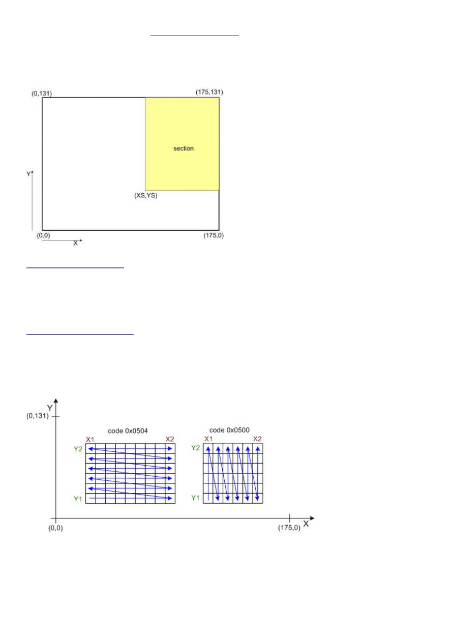
OR = 0x00
defines the
90 degree
orientation.
For details see the section
partial screen write
.
With
OR = 0x04
the memory is written in X-direction, that means line by line in X-
direction from left (low X-number) to right (high X-number).
With
OR = 0x00
the display memory is written in Y-direction, that means from column
by column from
YS
to
131
.
Pixel Color Coding:
The display memory is initialized to work according the -5-6-5- color coding
(-R-G-B-) scheme. That means the first (MSB first) 5-bits are coding the intensity of
red, the following 6-bits are coding the intensity of green and the last 5-bits the
intensity of blue. (0xFFFF is white, 0x0000 is black)
Partial Screen Write:
The display memory is organized in a matrix form with X- and Y coordinates.
At each matrix coordinate one 16-bit color value (pixel) is stored.
(Advanced techniques like PET (sub-pixel addressing) seems not to be supported.)
The following picture shows the principle:
For partial writing to the memory the commands below are used. The start corner
(
X1
,
Y1
) and the end corner (
X2
,
Y2
) have to be defined.
X2
has to be larger or equal
X1
,
Y2
has to be larger or equal
Y1
.
7
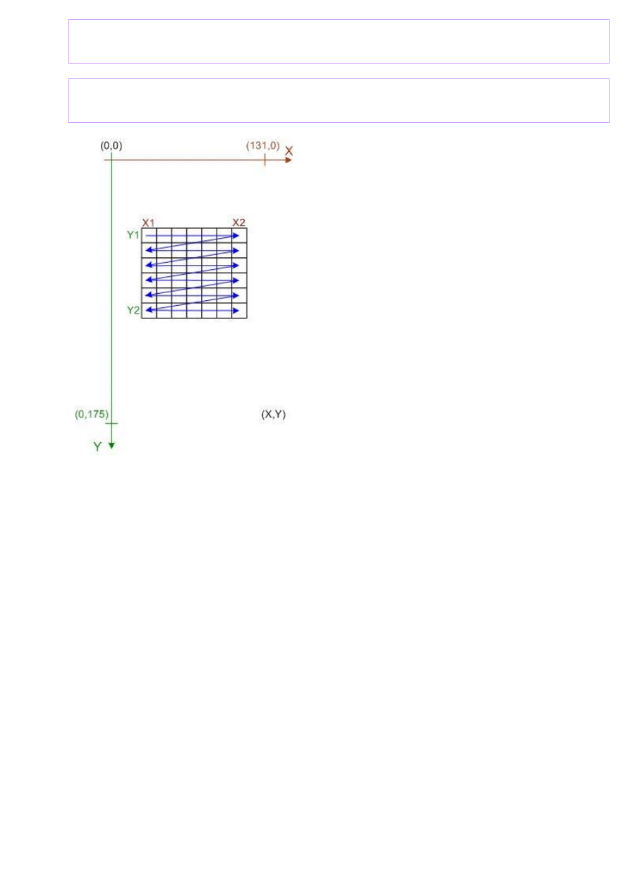
PMEMWRX: (X-direction)
0xEF90, 0x0504, 0x08
X1
, 0x09
X2
, 0x0A
Y1
, 0x0B
Y2
PMEMWRY: (Y-direction)
0xEF90, 0x0500, 0x08
X1
, 0x09
X2
, 0x0A
Y1
, 0x0B
Y2
The display memory can be written in
X
- or
Y
-direction. Other advanced memory
access modes are not supported.
Writing in
Y
-direction is usually prefered if the display is used 90-degree rotated. If
than the
X
- and
Y
-values in the PMEMWRY command are exchanged, the coordination
system - shown in the left picture is obtained. In this case bitmaps are drawn from the
upper left corner down to the lower right corner.
8

9
More advanced RAM addressing modes (LS020)
Address Auto-Increment and Windowing
The display controller generates the addresses of the integrated display-RAM
automatically. For that a window has to be defined in the display RAM.
If data is written to the display RAM the data is displayed in that window.
Depending on the address generating sequence the data is written in different
modes to this window. This code shows how to write a rectangular bitmap image
to the display memory. Pixels are drawn with textcolor, the background is drawn
with backcolor. The image is stored as bit-array in the ascii_tab. array.
// image size is 8x14
uint8_t ascii_tab[14]={ 0x00, 0x00, 0x00, 0xfc, 0x66, 0x66, 0x66, 0x7c, 0x66, 0x66, 0x66, 0xfc,
0x00, 0x00},
for (h=0; h < CHAR_H; h++) // every column of the picture y-direction (mode 0)
{
ch=ascii_tab[h];
mask=0x80;
for (p=0; p < CHAR_W; p++) // write the pixels in x direction (mode 0)
{
if (ch & mask) {
lcd_wrdat16(textcolor);
}
else {
lcd_wrdat16(backcolor);
}
mask=mask/2;
}
}
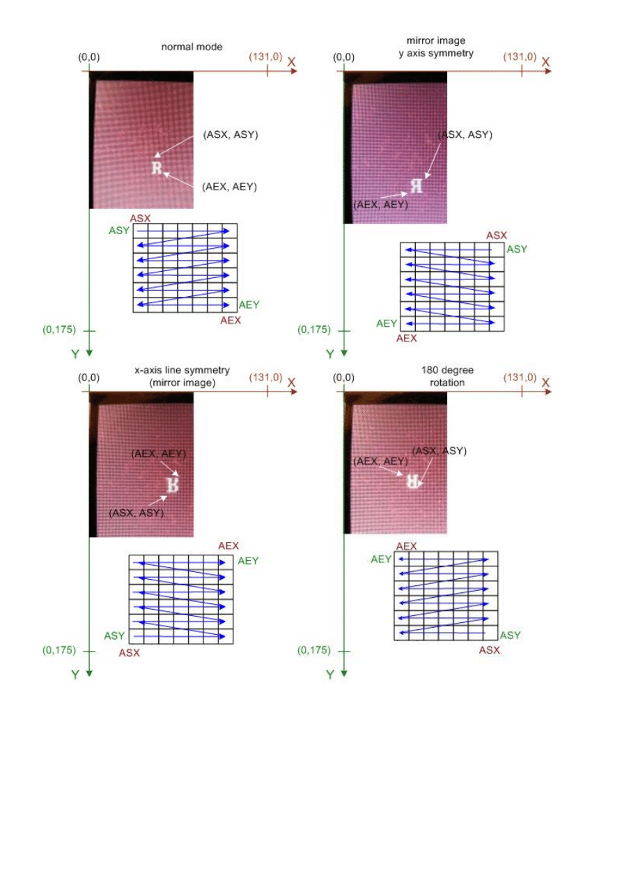
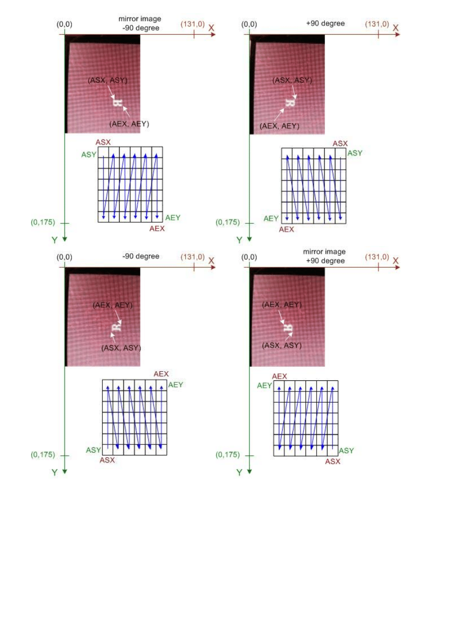
Address generating sequence
The order of the automatically generated addresses can be programmed.
That means by using the same drawing routine the picture will appear in different
orientations on the screen. For example the picture can be rotated by 90, 180 or 270
degree before it appears on the screen.
The following pictures are showing all possible orientations:
10
11
12
The given programming sequences are using the definition of the picture writing routine
above. Note that the width (CHAR_W) and the height (CHAR_H) have to be swapped, if
the image is displayed in a 90 degree rotation. Inital, before starting data writing and
address mode changing, the register have to be defined and the addressing mode has
to be set using the following code sequence:
#define
ASX
0x1200
#define
ASY
0x1300
#define
APX
0x1400
#define
AEX
0x1500
#define
AEY
0x1600
#define
APY
0x1700
lcd_wrcmd16(0xEF80);
In the table you find the code for the mode change and the window definition code.
Mode
Programming
normal mode
lcd_wrcmd16(0x1800);
lcd_wrcmd16(
ASX
+x);
lcd_wrcmd16(
AEX
+x+(CHAR_W-1));
lcd_wrcmd16(
ASY
+y);
lcd_wrcmd16(
AEY
+y+(CHAR_H-1));
y-axis symmetry (mirror image)
lcd_wrcmd16(0x1801);
lcd_wrcmd16(
ASX
+x);
lcd_wrcmd16(
AEX
+x-(CHAR_W-1));
lcd_wrcmd16(
ASY
+y);
lcd_wrcmd16(
AEY
+y+(CHAR_H-1));
x-axis line symmetry (mirror image)
lcd_wrcmd16(0x1802);
lcd_wrcmd16(
ASX
+x);
lcd_wrcmd16(
AEX
+x+(CHAR_W-1));
lcd_wrcmd16(
ASY
+y);
lcd_wrcmd16(
AEY
+y-(CHAR_H-1));
180 degree rotation
lcd_wrcmd16(0x1803);
lcd_wrcmd16(
ASX
+x);
lcd_wrcmd16(
AEX
+x-(CHAR_W-1));
lcd_wrcmd16(
ASY
+y);
lcd_wrcmd16(
AEY
+y-(CHAR_H-1));
mirror image, -90 degree
lcd_wrcmd16(0x1804);
lcd_wrcmd16(
ASX
+x);
lcd_wrcmd16(
AEX
+x+(CHAR_W-1));
lcd_wrcmd16(
ASY
+y);
lcd_wrcmd16(
AEY
+y+(CHAR_H-1));
+90 degree
lcd_wrcmd16(0x1805);
lcd_wrcmd16(
ASX
+x);
lcd_wrcmd16(
AEX
+x-(CHAR_H-1));
lcd_wrcmd16(
ASY
+y);
lcd_wrcmd16(
AEY
+y+(CHAR_W-1));
-90 degree
lcd_wrcmd16(0x1806);
lcd_wrcmd16(
ASX
+x);
lcd_wrcmd16(
AEX
+x-(CHAR_H-1));
lcd_wrcmd16(
ASY
+y);
lcd_wrcmd16(
AEY
+y-(CHAR_W-1));
+90 degree (mirror image)
lcd_wrcmd16(0x1807);
lcd_wrcmd16(
ASX
+x);
lcd_wrcmd16(
AEX
+x-(CHAR_H-1));
lcd_wrcmd16(
ASY
+y);
lcd_wrcmd16(
AEY
+y-(CHAR_W-1));

13
II) LPH - Display:
Description of init sequence not ready yet. Please look at the example code on: (
http://www.superkranz.de/christian/S65_Display/DisplayIndex.html
)
Power Down:
0x74 0x00 0x0D
0x76 0x05 0x05
0x74 0x00 0x0E
0x76 0x1D 0x1F
0x74 0x00 0x03
0x76 0x00 0x00
III) L2F50 - Display:
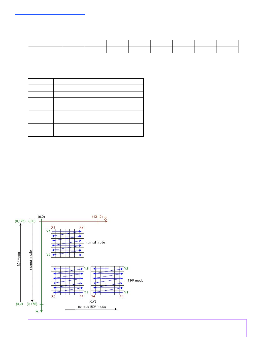
Currently two different drawing modes are known. The normal mode and 180degree
rotated mode. The graphic modes are programmed using the parameter of the
DATCTL
command.
DATCTL 7 6 5 4 3 2 1 0
parameter
x *
1
*
C2
*
C1
G
Not all parameter bit combinations are known today. The next table shows the meaning
of known bits.
Bit Discription
x no
influence
*
if set memory not written
C1
/
C2
0
0
= not working
0
1
= different color coding
1
0
= not working
1
1
= 5-6-5 color coding (16-bit)
G 0
= normal mode
1
= 180 deg. mode
Writing in the different graphic modes is shown in the following figure.
In normal mode the (0,0) point is in the left upper corner.
The (
X
,
Y
) coordinates for the SD_CSET and SD_PSET commands are given in natural
order. (
X1
,
Y1
) is the upper left corner, (
X2
,
Y2
) is the lower right corner.
In 180 degree mode things are a little bit more confusing. The
Y
-axis changes the
direction, but
X
-axis not. In addition, if a rectangular area is drawn, (
X1
,
Y1
) is now the
lower right corner of the rectangle and (
X2
,
Y2
) is the upper left corner, but still
X1
has
to be lower than
X2
and
Y1
has to be lower than
Y2
. That means if e.g.
X1
=0 and
X2
=15 the rectangular is drawn from starting at
X
=15 with the first bit. Then it is
drawn down to
X
=0 ending with the 16'th bit.
Power Down:
14
0x8E00 - Command
Reengineering the S65 Display:
The Siemens S65 display is a special manufacturing for the Siemens AG (now
Siemens/BenQ). Because of that it is very difficult to get data sheets for the used
display controller. The display is a product of Seiko-Epson but does not response to the
known Epson display commands (also not to the commands of relative new Epson 16-
bit controller). Because of that I decided to do a re-engineering of the display interface
using a S65 mobile phone.
It was easy to figure out that Siemens uses a serial two wire interface with additional
chip select, a command/data signal (usually called RS) and a reset signal. The clock
frequency of the serial interface is 13MHz. Supply voltages are 2.9V for the display
driver and 1.8V for the digital interface. In addition there are two supply pins for the
four white backlight LED's. The LED's are serial connected and buffered with a
capacitance on the display board. The serial connection ensures a very constant light
intensity distribution. That is because each LED is driven by the same current. The
disadvantage is that a relative high voltage is needed for driving the LED’s. The LED
voltage was measured to 10.4V at 20mA for one display. But in the hardware section
you can see that it is not very difficult to generate the voltage with a PWM signal
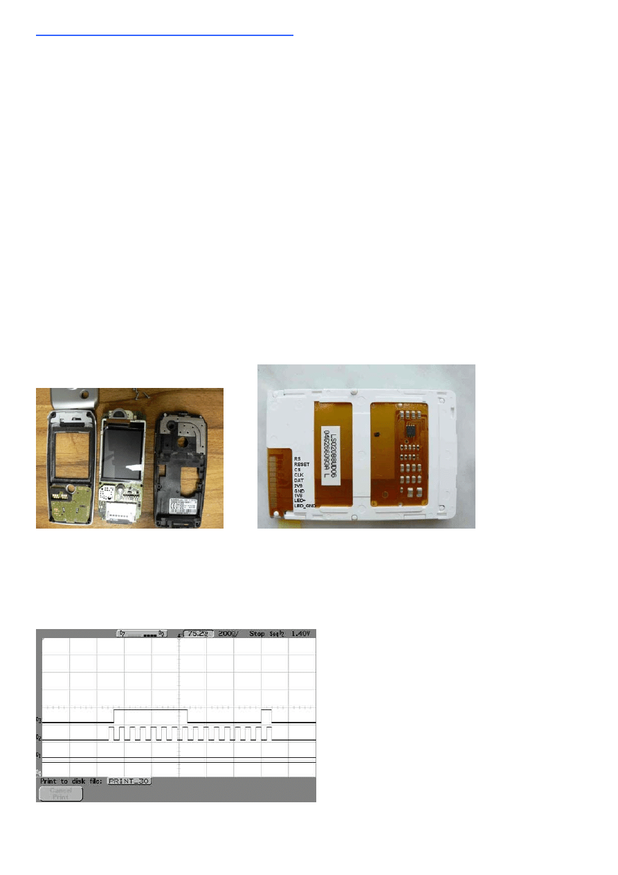
generated by the µC. The display pin out can be seen on the figure on the left side. CS
is the chip select line, CLK the clock line, DAT the data line, RS the command/data
identification, 2V9 the 2.9V supply, 1V8 the 1.8V supply, LED+ the positive LED supply
and LED_GND the negative LED supply.
The display interface was measured using a HP (Agilent) 16-channel digital oscilloscope.
(unfortunately a logic analyser was not available)
The display commands and data are written in a 16-bit format like the example on the
picture. A data bit is latched with the rising edge of the clock signal by the display
controller.
15

16
Start Up Sequence:
The following sequences for starting the display could be identified:
Sequence 1: (time 0ms)
0xFDFD,
0xFDFD
Sequence 2: (time 68ms after start)
0xEF00, 0xEE04, 0x1B04, 0xFEFE, 0xFEFE
0xEF90, 0x4A04, 0x7F3F, 0xEE04, 0x4306
Sequence 3: (time 75ms after start)
0xEF90, 0x0983, 0x0800, 0x0BAF, 0x0A00, 0x0500, 0x0600, 0x0700
0xEF00
0xEE0C
0xEF90, 0x0080,
0xEFB0,
0x4902
0xEF00
0x7F01,
0xE181
Sequence 4: (time 182ms after start)
0xE202
Sequence 5: (time 297ms after start)
0xE276
Sequence 6: (time 401ms after start)
0xE183
Sequence 7: (time 460ms after start)
0x8001
In addition it could be measured, that Siemens always refreshes the screen
at once. That means also if only parts of the screen are changed the complete display
memory is refreshed. Reason for that is, that Siemens uses an display graphic
controller like the s1d13732. This controller holds the display memory and writes the
display content via hardware.
Only the commands are generated by the µC. The sequence used by Siemens for
writing the compete display is:
write complete display memory:
0xEF90, 0x0500, 0x0600, 0x0700
After that the display data follows (with RS line low). Writing the display data takes
28.59ms which corresponds to (132*176*16=371712 bits with 13MHz clock frequency.

17
Power Down Sequence:
Unfortunately the power down sequence could not be measured with the used
equipment. It was not possible to find a proper trigger condition to get a reliable
repeatable measurement of the power down sequence.
Triggering to the backlight was possible but the memory of the digital scope was to
small to catch the sequences. Unfortunately the backlight is switched off after the
display is powered down. Spending more effort it might be possible to catch the power
down sequence but that is not done up to now. The proposed sequence so far is reset
of display and switching off the supply.
Document Outline
- About the Display
- Hardware
- I) LS020 - Display
- II) LPH - Display
- III) L2F50 - Display
- Reengineering the S65 Display
Wyszukiwarka
Podobne podstrony:
11 3 4 6 Lab Using the CLI to Gather Network?vice Information
Kolorowy wyświetlacz graficzny z telefonu Siemens S65 M65 z kontrolerem Hitachi HD66773, cz 3
DUI0379C using the assembler
Roszak, Rewers, Pliszka USING THE 3D
Barron Using the standard on objective measures for concert auditoria, ISO 3382, to give reliable r
11 3 4 6 Lab Using the CLI to Gather Network (2)
Using the PSpice Library Translator
A ZVS PWM Inverter With Active Voltage Clamping Using the Reverse Recovery Energy of the Diodes
Developing your STM32VLDISCOVERY application using the MDK ARM
Developing your STM32VLDISCOVERY application using the Atollic TrueSTUDIO
Ch5 Using the Tutorials
DUI0473C using the arm assembler
8 1 2 7 Lab Using the Windows?lculator with Network?dresses
Kolorowy wyświetlacz graficzny z telefonu Siemens S65 M65 z kontrolerem Hitachi HD66773, cz 2
Guide to using the tests
Introduction to business modeling using the UML
guide to using the tests Notatek pl
Assessment of Borderline Pathology Using the Inventory of Interpersonal Problems Circumplex Scales (
Trieste The City as Displaced Persons Camp Pamela Ballinger
więcej podobnych podstron