
ð
Developer Press
Apple Computer, Inc. 1995
ð
Developer Note
Power Macintosh 5200/75 and
Power Macintosh 6200/75
Computers

ð
Apple Computer, Inc.
1995 Apple Computer, Inc.
All rights reserved.
No part of this publication may be
reproduced, stored in a retrieval
system, or transmitted, in any form or
by any means, mechanical, electronic,
photocopying, recording, or otherwise,
without prior written permission of
Apple Computer, Inc. Printed in the
United States of America.
The Apple logo is a trademark of
Apple Computer, Inc.
Use of the “keyboard” Apple logo
(Option-Shift-K) for commercial
purposes without the prior written
consent of Apple may constitute
trademark infringement and unfair
competition in violation of federal and
state laws.
No licenses, express or implied, are
granted with respect to any of the
technology described in this book.
Apple retains all intellectual property
rights associated with the technology
described in this book. This book is
intended to assist application
developers to develop applications only
for Apple Macintosh computers.
Every effort has been made to ensure
that the information in this manual is
accurate. Apple is not responsible for
printing or clerical errors.
Apple Computer, Inc.
1 Infinite Loop
Cupertino, CA 95014
408-996-1010
Apple, the Apple logo, APDA,
AppleLink, Apple SuperDrive,
LaserWriter, LocalTalk, Macintosh,
Macintosh Centris, Macintosh Quadra,
PlainTalk, PowerBook and QuickTime
are trademarks of Apple Computer,
Inc., registered in the United States and
other countries.
Apple Desktop Bus, Mac, and Power
Macintosh are trademarks of Apple
Computer, Inc.
Adobe Illustrator and PostScript are
trademarks of Adobe Systems
Incorporated, which may be registered
in certain jurisdictions.
America Online is a registered service
mark of America Online, Inc.
CompuServe is a registered service
mark of CompuServe, Inc.
FrameMaker is a registered trademark
of Frame Technology Corporation.
Helvetica and Palatino are registered
trademarks of Linotype Company.
ITC Zapf Dingbats is a registered
trademark of International Typeface
Corporation.
Motorola is a registered trademark of
Motorola Corporation.
NuBus is a trademark of Texas
Instruments.
PowerPC is a trademark of
International Business Machines
Corporation, used under license
therefrom.
Simultaneously published in the United
States and Canada.
LIMITED WARRANTY ON MEDIA AND
REPLACEMENT
If you discover physical defects in the
manual or in the media on which a software
product is distributed, APDA will replace
the media or manual at no charge to you
provided you return the item to be replaced
with proof of purchase to APDA.
ALL IMPLIED WARRANTIES ON THIS
MANUAL, INCLUDING IMPLIED
WARRANTIES OF MERCHANTABILITY
AND FITNESS FOR A PARTICULAR
PURPOSE, ARE LIMITED IN DURATION
TO NINETY (90) DAYS FROM THE DATE
OF THE ORIGINAL RETAIL PURCHASE
OF THIS PRODUCT.
Even though Apple has reviewed this
manual, APPLE MAKES NO WARRANTY
OR REPRESENTATION, EITHER EXPRESS
OR IMPLIED, WITH RESPECT TO THIS
MANUAL, ITS QUALITY, ACCURACY,
MERCHANTABILITY, OR FITNESS FOR A
PARTICULAR PURPOSE. AS A RESULT,
THIS MANUAL IS SOLD “AS IS,” AND
YOU, THE PURCHASER, ARE ASSUMING
THE ENTIRE RISK AS TO ITS QUALITY
AND ACCURACY.
IN NO EVENT WILL APPLE BE LIABLE
FOR DIRECT, INDIRECT, SPECIAL,
INCIDENTAL, OR CONSEQUENTIAL
DAMAGES RESULTING FROM ANY
DEFECT OR INACCURACY IN THIS
MANUAL, even if advised of the possibility
of such damages.
THE WARRANTY AND REMEDIES SET
FORTH ABOVE ARE EXCLUSIVE AND IN
LIEU OF ALL OTHERS, ORAL OR
WRITTEN, EXPRESS OR IMPLIED. No
Apple dealer, agent, or employee is
authorized to make any modification,
extension, or addition to this warranty.
Some states do not allow the exclusion or
limitation of implied warranties or liability
for incidental or consequential damages, so
the above limitation or exclusion may not
apply to you. This warranty gives you
specific legal rights, and you may also have
other rights which vary from state to state.

iii
Contents
Figures and Tables
vii
Preface
About This Note
ix
Contents of This Note
ix
Supplemental Reference Documents
x
Information About Earlier Models
x
For More Information
xi
Conventions and Abbreviations
xi
Typographical Conventions
xi
Standard Abbreviations
xii
Chapter 1
Introduction
1
Summary of Features
2
Comparison With Macintosh Quadra/LC 630 Series Computers
3
External Features
4
Front View
4
Back View
5
Access to the Logic Board
6
Front Panel Push Buttons
6
Power On and Off
7
Optional Features
7
TV Tuner
7
Video Input
8
Video Display Mirror Out
9
Communications
9
Compatibility Issues
10
Microprocessor Differences
10
POWER-Clean Code
10
Completion Serialized Instructions
10
Split Cache
11
Data Alignment
11
Expansion Slot
11
IDE Hard Disk
12

iv
Chapter 2
Architecture
13
Block Diagram and Main ICs
14
Microprocessor
14
Second-Level Cache and ROM
16
System RAM
16
Custom ICs
16
Capella IC
16
F108 IC
17
PrimeTime II IC
17
DFAC II IC
18
Cuda IC
18
Valkyrie IC
19
Bus Arbitration
19
Display RAM
20
Address Map
21
RAM Addresses
21
Display RAM Addresses
21
Addresses for PDS Expansion Cards
21
Chapter 3
I/O Features
23
Serial I/O Ports
24
ADB Port
25
Floppy Disk Drive
26
IDE Hard Disk
27
Hard Disk Specifications
27
Hard Disk Connectors
27
Pin Assignments
29
IDE Signal Descriptions
30
SCSI Bus
30
SCSI Connectors
31
SCSI Bus Termination
32
Sound
32
Sound Output
32
Sound Input
32
Sound Input Specifications
33
Routing of the Sound Signals
33
Digitizing Sound
33
Sound Modes
34
Keyboard
34
Video
35
Optional Video Display Mirror Output Feature
35
External Video Monitors
36
External Video Connection for Power Macintosh 6200
37
Video Timing Parameters
38

v
Chapter 4
Expansion Features
43
RAM Expansion
44
RAM Configurations
44
Signals on the RAM SIMM Slot
45
RAM Devices
47
Addressing RAM
48
RAM SIMM Mechanical Specifications
49
The I/O Expansion Slot
51
The I/O Expansion Connector
51
Connector Pin Assignments
51
Signal Descriptions
53
Bus Master on a Card
56
Incompatibility With Older Cards
56
Designing an I/O Expansion Card
57
Card Connectors
57
Power for the Card
57
Card Address Space
58
Card Select Signal
58
The DVA Connector
59
Pin Assignments
60
Signal Descriptions
61
Using the YUV Bus
61
Video Data Format
62
The Communications Slot
63
Chapter 5
Software Features
67
ROM Software
68
Machine Identification
68
System Software
68
Chapter 6
Software for the IDE Hard Disk
71
Introduction to IDE Software
72
IDE Hard Disk Device Driver
73
ATA Manager
73
IDE Hard Disk Driver Reference
74
High-Level Device Manager Functions
74
open
74
close
75
prime
75
status
76
control
76

vi
IDE Hard Disk Driver Control Functions
77
killIO
77
verify
77
format
78
ejectMedia
78
return drive icon
78
return media icon
79
return drive characteristics
79
needTime code
80
power management
80
drive status info
81
return driver gestalt
81
power-mode status
83
ATA Manager Reference
83
The ATA Parameter Block
83
Functions
88
ATA_ExecIO
89
ATA_MgrInquiry
92
ATA_MgrInit
93
ATA_BusInquiry
93
ATA_QRelease
95
ATA_NOP
96
ATA_Abort
96
ATA_RegAccess
97
ATA_Identify
98
ATA_ResetBus
99
ATA_MgrShutDown
99
ATA_DrvrRegister
100
ATA_DrvrDeregister
100
ATA_FindRefNum
101
Error Code Summary
102
Appendix
Foldout Drawings
105
Index
113

vii
Figures and Tables
Chapter 1
Introduction
1
Figure 1-1
Front view of the computer
5
Figure 1-2
Back view of the computer
6
Table 1-1
Comparison with the Macintosh Quadra/LC 630 series
computers
3
Chapter 2
Architecture
13
Figure 2-1
System Block diagram
15
Figure 2-2
Simplified address map
22
Chapter 3
I/O Features
23
Figure 3-1
Serial port sockets
24
Figure 3-2
Maximum dimensions of the hard disk
28
Figure 3-3
Video timing diagram
39
Table 3-1
Serial port signals
24
Table 3-2
ADB connector pin assignments
25
Table 3-3
Pin assignments on the floppy disk connector
26
Table 3-4
Pin assignments on the IDE hard disk connector
29
Table 3-5
Signals on the IDE hard disk connector
30
Table 3-6
Pin assignments for the SCSI connectors
31
Table 3-7
Sound sources and routing
33
Table 3-8
Reset and NMI key combinations
34
Table 3-9
Video mirror connector pin assignments
35
Table 3-10
Maximum pixel depths for video monitors
36
Table 3-11
Pin assignments for external video connector
37
Table 3-12
Monitors supported
38
Table 3-13
Video timing parameters for smaller monitors
40
Table 3-14
Video timing parameters for larger monitors
41
Chapter 4
Expansion Features
43
Figure 4-1
RAM expansion SIMM
50
Figure 4-2
Generating the card select signal
58
Figure 4-3
Location of the DVA connector
59
Figure 4-4
Orientation of the DVA connector
60
Figure 4-5
Video data timing
62
Table 4-1
RAM configurations
44
Table 4-2
Signal assignments on the RAM SIMM slot
45

viii
Table 4-3
Address multiplexing for DRAM devices
48
Table 4-4
Address modes for various DRAM devices
49
Table 4-5
Pin assignments for the expansion connector
52
Table 4-6
Descriptions of the signals on the I/O expansion connector
54
Table 4-7
Power available for the expansion card
58
Table 4-8
Pin assignments on the DVA connector
60
Table 4-9
Descriptions of the signals on the DVA connector
61
Table 4-10
Pin assignments for the communucations slot connector
63
Chapter 6
Software for the IDE Hard Disk
71
Figure 6-1
Relationship of the ATA Manager to the Macintosh system
architecture
72
Figure 6-2
IDE hard disk drive icon
78
Table 6-1
Status functions supported by the IDE hard disk driver
76
Table 6-2
IDE drive bus states
86
Table 6-3
Control bits in the
ataFlags
field
86
Table 6-4
ATA Manager functions
88
Table 6-5
IDE register selectors
97
Table 6-6
IDE hard disk drive error codes
102
Appendix
Foldout Drawings
105
Foldout 1
Expansion card design guide
Foldout 2
Expansion card component height restrictions
Foldout 3
Expansion card assembly guide

ix
P R E F A C E
About This Note
This developer note describes the Power Macintosh 5200/75 and
Power Macintosh 6200/75 computers and emphasizes features that are
new or different from previous Macintosh models. It is intended to help
experienced Macintosh hardware and software developers design compatible
products. If you are unfamiliar with Macintosh computers or would simply
like more technical information, you may wish to read the related technical
manuals listed in the section “Supplemental Reference Documents.”
Contents of This Note
0
The information is arranged in six chapters, an appendix, and an index:
■
Chapter 1, “Introduction,” gives a summary of the features of the Power
Macintosh 5200 and 6200 computers, describes the physical appearance of
the two models, and lists the available configurations and options.
■
Chapter 2, “Architecture,” describes the internal organization of the compu-
ters. It includes a block diagram and descriptions of the main components
of the logic board.
■
Chapter 3, “I/O Features,” describes the built-in I/O devices and the
external I/O ports. It also describes the built-in monitor configuration of
the Power Macintosh 5200 and external video monitors that can be used
with both computers.
■
Chapter 4, “Expansion Features,” describes the expansion slots of the
Power Macintosh 5200 and 6200 computers. This chapter provides guide-
lines for designing cards for the I/O expansion slot and brief descriptions
of the expansion modules for the other slots.
■
Chapter 5, “Software Features,” summarizes the new features of the ROM
software and the system software that accompany the Power Macintosh
5200 and 6200 computers.
■
Chapter 6, “Software for the IDE Hard Disk,” gives the program interface
for the system software and the driver that support the internal IDE hard
disk drive.
■
The appendix includes foldout pages with mechanical drawings for the
I/O expansion card described in Chapter 4.

x
P R E F A C E
Supplemental Reference Documents
0
To supplement the information in this developer note, developers should
have copies of the appropriate Motorola reference books for the
PowerPC
603 microprocessor. Software developers should have a copy
of Motorola’s
PowerPC Programmer’s Reference Manual.
Hardware developers
should have copies of Motorola’s
PowerPC 603 RISC Microprocessor User’s
Manual
and the
MC68030 User’s Manual.
For additional information about the digital data format used in the video
input module, refer to
Macintosh DAV Interface for NuBus Expansion Cards,
part
of
Macintosh Developer Note Number 8,
APDA catalog number R0566LL/A
.
For
information about the digital video interface, refer to the
SAA7194/6 Philips
Desktop Video Handbook
.
Developers may also need copies of the appropriate Apple reference books.
You should have the relevant books of the
Inside Macintos
h series, and
particularly
Inside Macintosh: QuickTime Components.
You should also have
Guide to the Macintosh Family Hardware,
second edition, and
Designing Cards
and Drivers for the Macintosh Family,
third edition. These books are available in
technical bookstores and through APDA.
Information About Earlier Models
0
Many features of the Macintosh 5200 and 6200 computers are similar to those
of certain earlier Macintosh models, so you may wish to have the developer
notes that describe those earlier machines:
■
Macintosh Developer Note Number 3,
APDA catalog number R0461LL/A
■
Macintosh Developer Note Number 4,
APDA catalog number R0528LL/A
■
Macintosh Developer Note Number 6,
APDA catalog number R0550LL/A
■
Macintosh Developer Note Number 10,
APDA catalog number R0568LL/A
Macintosh Developer Note Number 3
includes information about the
Macintosh LC III and the Macintosh Centris 610 and 650 computers.
Macintosh Developer Note Number 4
includes information about the
Macintosh LC 520 computer.
Macintosh Developer Note Number 6
includes
information about the Macintosh LC 475 and Macintosh Quadra 605
computers.
Macintosh Developer Note Number 10
includes information about
the Macintosh Quadra 630 and the Macintosh LC 630 computers.
The numbered developer notes are available from APDA. Developer notes for
individual models are also on the developer CDs.

xi
P R E F A C E
For More Information
0
APDA is Apple Computer’s worldwide source for hundreds of development
tools, technical resources, training products, and information for anyone
interested in developing applications on Apple platforms. Customers receive
the
APDA Tools Catalog
featuring all current versions of Apple development
tools and the most popular third-party development tools. APDA offers
convenient payment and shipping options, including site licensing.
To order products or to request a complimentary copy of the
APDA Tools
Catalog
, contact
APDA
Apple Computer, Inc.
P.O. Box 319
Buffalo, NY 14207-0319
Conventions and Abbreviations
0
This developer note uses the following typographical conventions and
abbreviations.
Typographical Conventions
0
New terms appear in
boldface
where they are first defined.
Computer-language text—any text that is literally the same as it appears in
computer input or output—appears in
Courier
font.
Hexadecimal numbers are preceded by a dollar sign ($). For example, the
hexadecimal equivalent of decimal 16 is written as $10.
Note
A note like this contains information that is interesting but not essential
for an understanding of the text.
◆
Telephone
1-800-282-2732 (United States)
1-800-637-0029 (Canada)
716-871-6555 (International)
Fax
716-871-6511
AppleLink
APDA
America Online
APDAorder
CompuServe
76666,2405
Internet
APDA@applelink.apple.com

xii
P R E F A C E
IMPORTANT
A note like this contains important information that you should read
before proceeding.
▲
▲
W A R N I N G
A note like this directs your attention to something that could cause
damage or result in a loss of data.
▲
Standard Abbreviations
0
When unusual abbreviations appear in this book, the corresponding terms are
also spelled out. Standard units of measure and other widely used
abbreviations are not spelled out. Here are the standard units of measure
used in this developer note:
Here are other abbreviations used in this developer note:
A
amperes
mA
milliamperes
dB
decibels
µ
A
microamperes
GB
gigabytes
MB
megabytes
Hz
hertz
MHz
megahertz
in.
inches
mm
millimeters
k
1000
ms
milliseconds
K
1024
µ
s
microseconds
KB
kilobytes ns
nanoseconds
kg
kilograms
Ω
ohms
kHz
kilohertz sec.
seconds
k
Ω
kilohms
V
volts
lb.
pounds
W
watts
$
n
hexadecimal
value
n
AC
alternating current
ADB
Apple Desktop Bus
CD-ROM
compact-disk read-only memory
CLUT
color lookup table
continued
Sidebar
information about a related subject, or technical details
that are not required reading.
Sidebars are for digressions—information that is not
part of the main discussion. A sidebar may contain
background information that is interesting to know,

xiii
P R E F A C E
DESC
digital video decoder and scaler
DIMM
dual inline memory module
DRAM
dynamic random-access memory
EMI
electromagnetic interference
FPU
floating-point unit
IC
integrated circuit
IDE
integrated device electronics
IIC
inter-integrated circuit (an internal control bus)
I/O
input/output
IR
infrared
LS TTL
low-power Schottky TTL (a standard type of device)
MMU
memory management unit
MOS
metal-oxide semiconductor
NTSC
National Television Standards Committee (the standard system
used for broadcast TV in North America and Japan)
NMI
nonmaskable interrupt
PAL
Phase Alternating Line system (the standard for broadcast TV
in most of Europe, Africa, South America, and southern Asia)
PDS
processor-direct slot
PWM
pulse-width modulation
RAM
random-access memory
RGB
a video signal format with separate red, green, and blue
components
RISC
reduced instruction set computing
RMS
root-mean-square
ROM
read-only memory
SANE
Standard Apple Numerics Environment
SCSI
Small Computer System Interface
SCC
serial communications controller
SECAM
the standard system used for broadcast TV in France and the
former Soviet countries
SIMM
single inline memory module
S-video
a type of video connector that keeps luminance and
chrominance separate; also called a Y/C connector
SWIM
Super Woz Integrated Machine, a custom IC that controls the
floppy disk interface
TTL
transistor-transistor logic (a standard type of device)
VCR
video cassette recorder
VLSI
very large scale integration
continued

xiv
P R E F A C E
VRAM
video RAM; used for display buffers
Y/C
a type of video connector that keeps luminance and
chrominance separate; also called an S-video connector
YUV
a video signal format with separate luminance and
chrominance components

C H A P T E R 1
Introduction
1
Figure 1-0
Listing 1-0
Table 1-0

C H A P T E R 1
Introduction
2
Summary of Features
The Power Macintosh 5200/75 and 6200/75 computers are new Macintosh models that
incorporate a PowerPC
603 microprocessor running at 75 MHz, a built-in cache, and
the same AV features (audio and video input and output) as the Macintosh LC 630 and
Macintosh Quadra 630 computers. The Power Macintosh 5200 is housed in a new
all-in-one enclosure featuring a 15-inch monitor with tilt and swivel capability and stereo
speakers. The Power Macintosh 6200 is functionally identical to the Power Macintosh 5200
but has a low-profile case similar to the Macintosh Quadra 630 and requires an external
monitor.
Summary of Features
1
Here is a summary of the hardware features of the Power Macintosh 5200 and 6200
computers. Each feature is described more fully later in this note.
■
Microprocessor: PowerPC 603 microprocessor running at 75 MHz.
■
RAM: 8 MB standard using 4 Mbit DRAM devices installed in one 72-pin DRAM
SIMM; expandable to 64 MB using 16-Mbit devices. Two SIMM slots are provided.
■
ROM: 4 MB on a 160-pin DIMM card; 64-bit ROM data bus width.
■
Cache: 256 KByte second-level (L2) cache on same 160-pin DIMM card as ROM.
■
Video configuration: internal video supports built-in 15-inch multiscan monitor on
Power Macintosh 5200 and external monitor on Power Macintosh 6200; external 1 MB
DRAM frame buffer on main logic board.
■
Video modes supported: 640
×
480 @ 16 bits, 600
×
800 @ 8 bits, and 632
×
824 @ 8 bits
(no video in).
■
Video input: 60 pin connector supports optional video card for real-time video
display, capture, and overlay.
■
Video output: video mirror feature allows an external monitor to be connected to
Power Macintosh 5200 using an optional video buffer board connected to the video
mirror connector. Power Macintosh 6200 supports up to 15-inch external monitors.
■
Sound: 8 bits/channel stereo sound output and mono sound input, external jack for
sound in, front and rear jacks for stereophonic sound out. The Power Macintosh 5200
has two built-in stereo speakers; the Power Macintosh 6200 has one speaker.
■
TV receiver: optional internal TV tuner.
■
Remote control: infrared (included with TV tuner configurations).
■
Hard disks: one internal 3.5-inch IDE hard disk with 500 MB capacity; external SCSI
port for additional SCSI devices.
■
Floppy disk: one internal 1.4 MB Apple SuperDrive.
■
CD ROM drive: internal SCSI connection for optional CD ROM drive.
■
Standard Macintosh I/O ports: two serial ports, sound input and output jacks, a SCSI
port, and an ADB port.

C H A P T E R 1
Introduction
Comparison With Macintosh Quadra/LC 630 Series Computers
3
■
Communications slot: 112-pin connector accepts an optional modem or Ethernet
interface.
■
Expansion slot: 114-pin connector accepts PDS cards designed for the
Macintosh LC series.
■
Power switch: soft power controlled from keyboard and remote control.
■
Case design: Power Macintosh 5200 has a new all-in-one enclosure featuring a tilt and
swivel monitor and built-in stereo speakers; Power Macintosh 6200 has a low-profile
case the same as the Macintosh Quadra 630.
Comparison With Macintosh Quadra/LC 630 Series
Computers
1
The Power Macintosh 5200 and 6200 computers are electrically similar to the Macintosh
Quadra 630 and LC 630. Table 1-1 compares the features of these computers.
Table 1-1
Comparison with the Macintosh Quadra/LC 630 series computers
Features
Power Macintosh 5200 and 6200
Macintosh LC 630 and
Macintosh Quadra 630
Processor type
PowerPC 603
MC68040 (in the Quadra 630)
MC68LC040 (in the LC 630)
Processor speed
75 MHz
66/33 MHz
Cache
256 KB second-level cache
none
Amount of RAM
8 MB–64 MB
4 MB–36 MB
RAM expansion
2 SIMM
1 SIMM
Video RAM
1 MB (DRAM)
1 MB (DRAM)
Video input
Optional card for video input,
capture, and overlay
Optional card for video input,
capture, and overlay
Video output
Optional mirror connector on
Power Macintosh 5200 supports
external monitor operating in
mirror mode; Power Macintosh
6200 supports up to 15-inch
external monitors at 16 bits per
pixel
Built-in video supports up to 15-inch
monitors at 16 bits per pixel
Sound capabilities
8 or 16 bits/channel; mono in,
stereo out
8 bits/channel; stereo in, mono
record, stereo out
Remote control
Built-in IR receiver
Built-in IR receiver
Floppy disk drive
One, internal
One, internal
continued

C H A P T E R 1
Introduction
4
External Features
External Features
1
The Power Macintosh 5200 has an integrated design featuring a built-in 15-inch
multi-scan color display with both tilt and swivel capabilities, stereo speakers, front
panel stereo headphone jack, and front panel push button controls for audio and video.
The Power Macintosh 6200 is functionally identical to the Power Macintosh 5200, but
uses a low-profile enclosure and requires an external monitor. This enclosure is identical
to the enclosures used for the Macintosh LC 630 and Macintosh Quadra 630 computers,
and is described in
Macintosh Developer Note Number 10.
This section describes only the Power Macintosh 5200 computer.
Front View
1
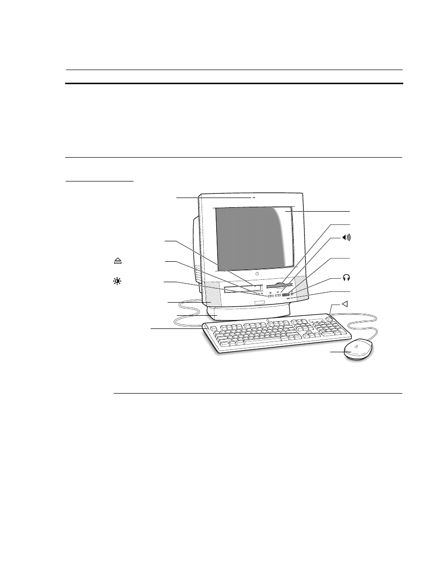
Figure 1-1 is a front view of a Power Macintosh 5200 computer. The front view shows the
display screen, the built-in microphone and stereo speakers, the openings for the floppy
disk and optional CD-ROM drive, the CD-ROM open and close button, the headphone
jack, the power-on light, the IR sensor for the remote control, and the push buttons that
control the sceen intensity and sound level.
ADB ports
1
1
Internal hard disk
One (IDE)
One (IDE)
Internal CD-ROM
optional
optional
External SCSI ports
One
One
Communications slot
One, for optional modem or
Ethernet interface
One, for optional modem or
Ethernet interface
Expansion slot
One I/O slot (accepts PDS card
for Macintosh LC series)
One I/O slot (accepts PDS card for
Macintosh LC series)
Table 1-1
Comparison with the Macintosh Quadra/LC 630 series computers
Features
Power Macintosh 5200 and 6200
Macintosh LC 630 and
Macintosh Quadra 630
C H A P T E R 1
Introduction
External Features
5
Figure 1-1
Front view of the computer
Back View
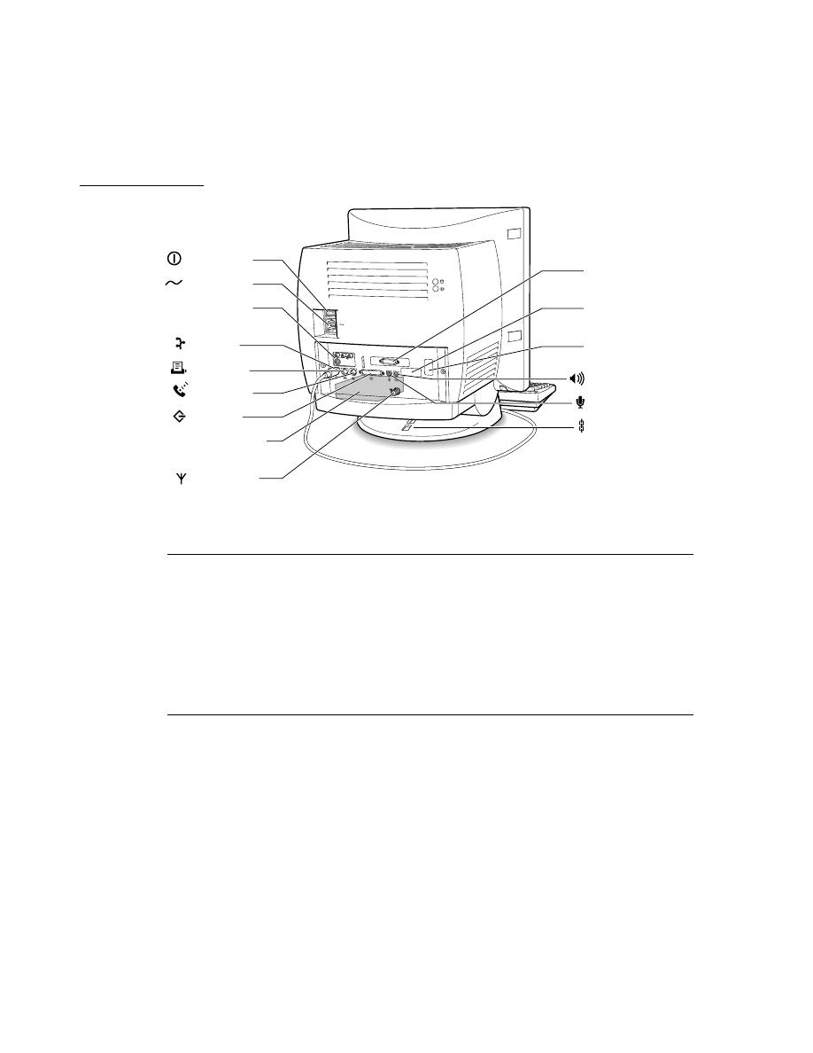
1
The back panel includes the power socket, the reset button, the I/O ports, and openings
for I/O access to the expansion modules: the I/O expansion card, the communications
card, and the video input card.
Mouse
Built-in microphone
Color display
Headphone jack
Floppy disk drive
Sound control
buttons
Screen control
buttons
Keyboard
CD-ROM drive
(optional)
Power-on light
CD-ROM drive
Open/Close button
Power key
Stereo speakers
Tilt and swivel base
Remote control
sensor
Why YUV Looks Clearer
blue, with the remaining bit unused. The YUV format
used in the Power Macintosh 5200 and 6200 computers
is also a 16-bit format, with 8 bits for the Y (luminance)
channel and 8 bits for the U and V (chrominance)
channels to share by multiplexing. The YUV format
looks clearer because the YUV format carries more
levels of luminance information.
You may be wondering how the digital YUV format
used in the Power Macintosh 5200 and 6200 computers
provides a clearer TV picture than the RGB format
used in the Macintosh TV computer—after all, picture
information can be freely converted between the two
formats. The difference is due to the way the bits are
allocated. The RGB format used in the Macintosh TV is
a 16-bit format using 5 bits each for red, green, and
C H A P T E R 1
Introduction
6
External Features
Figure 1-2 shows the back view of a Power Macintosh 5200 computer.
Figure 1-2
Back view of the computer
Access to the Logic Board
1
The logic board can be removed from the case to allow installation of expansion RAM or
a plug in an I/O expansion card. To get access to the logic board, you must first remove
the back panel. It is secured by two screws on either side of the I/O connectors. After
removing the screws, you can pull gently on the two latches on the underside of the
computer’s case and the back panel will slip out. You can then grasp the logic board
handle and pull the board straight out the back of the case.
Front Panel Push Buttons
1
The Power Macintosh 5200 computer has two pairs of push buttons on the front panel.
The pair on the left controls the intensity of the screen; the pair on the right controls the
sound level.
SCSI port
Monitor Out port
(optional)
LC-PDS card
access cover
Sound output port
Sound input port
Communication
card access cover
Security lock port
TV tuner card
(optional)
Power switch
Power socket
Hard disk drive
(internal)
Printer port
Modem port
ADB port
Video input card
(optional)

C H A P T E R 1
Introduction
Optional Features
7
Power On and Off
1
The user can turn the power on and off by pressing one of two buttons:
■
the Power key on the keyboard
■
the Power key on the remote control
If files are still open when the user attempts to turn off the computer by using either one
of the Power keys or the Shut Down menu item, the system displays an alert box
warning the user that files are open and should be closed to avoid loss of data.
Optional Features
1
Several features of the Power Macintosh 5200 and 6200 computers are implemented as
plug-in modules available either as a configuration option at the time of purchase or as a
later upgrade. The modules are designed so that they can be installed by the user.
TV Tuner
1
The TV tuner module turns the computer into a television receiver, complete with
remote control. The features of the TV tuner module are similar to those of the TV tuner
in the Macintosh Quadra 630 and LC 630 computers. The TV picture is in its own
window on the desktop, and the TV signal is carried in YUV format for improved
picture clarity.
The features of the TV tuner module are
■
ability to tune 181 broadcast and cable channels (United States version)
■
coaxial connector for TV antenna or cable input (F-type connector in United States
and Japanese versions; IEC-type connector in European versions)
■
TV picture in a resizable and movable window
■
YUV format for improved clarity (see sidebar)
■
support for closed captioning and teletext
■
software password protection
■
automatic and manual channel programming
■
single remote control for TV and for playback of audio CDs
The TV tuner module is available in versions for NTSC, PAL, and SECAM television
systems.
The TV picture appears in its own window. The default size of the window is 320-by-
240 pixels. The user can resize the TV window up to a maximum size of 640-by-
480 pixels or down to a minimum size of 160-by-120 pixels. The resolution of the TV
picture does not increase at the larger window sizes; instead, the image is enlarged by
doubling the size of the pixels.

C H A P T E R 1
Introduction
8
Optional Features
The TV tuner module works in conjunction with the video input module, which converts
the video data into digital YUV format and stores it in the display buffer.
The TV tuner comes with a remote control device similar to the one used with the
Macintosh TV computer. The user can switch channels either by using the remote control
or by typing the channel numbers on the keyboard. The user can toggle between the
current and previous channel by pressing the Tab key on the keyboard. Each time the
channel changes, the computer displays the channel name (assigned by the user) on the
picture in the video window.
The user can customize the operation of the TV tuner by adding or removing TV
channels that are unused or unwanted. The computer can program the channels
automatically, scanning through all available channels and disabling those that do not
have a valid signal. When the user then scans for the next channel by using the remote
control or the Tab key on the keyboard, the tuner skips the disabled channels.
The software that supports the TV tuner module is an application called Apple Video
Player. The application includes password protection for the disabled channels. Parents
might use this feature to prevent children from watching undesirable channels.
The software allows the user to capture or freeze a single frame of video or record a
segment of video as a QuickTime Movie. The TV window cannot be resized while the
computer is recording a movie.
Video Input
1
The video input card accepts video from an external source and displays it in a window
on the computer’s display. The following are features of the video input card:
■
accepts video input in NTSC, PAL, or SECAM format
■
connectors for stereo sound, composite video, and S-video (Y/C)
■
video display in a 320-by-240-pixel window
■
pixel doubling for 640-by-480-pixel maximum display
■
video overlay capability
■
YUV format for digital video input
■
a digital video connector for adding a video processor on an expansion card
The video input card provides AV features similar to those of the Macintosh
Quadra 660
AV
, with one key improvement. Whereas the Macintosh Quadra 660
AV
digitizes color video using a 16-bit RGB format, the video input card uses a digital YUV
format. Because a standard television signal has more information in its chrominance
channel than in its luminance channels, digitizing the video signal as YUV format results
in a clearer picture.
The video input card can accept video input from either an external device such as a
VCR or camcorder, or from the internal TV tuner module. The external device can be
connected to the video input card either through the composite video connector or the
S-video connector.

C H A P T E R 1
Introduction
Optional Features
9
The default window size is 320-by-240 pixels; the user can resize the window up to
640-by-480 pixels—the full screen on a 14-inch monitor. The large image uses pixel
doubling of the 320-by-240 pixel image.
Note
The video input card does not work on all video monitors. It will work
with 800-by-600-pixel displays that have a 60 Hz refresh rate, but not
with that size display at a 72 Hz refresh rate.
◆
The video input card plugs into a dedicated slot on the main logic board. The slot
connector is a 60-pin microchannel connector. The module fits only its proper slot and
only in the proper orientation so that the user can safely install the video input card.
The video input card has a separate connector called the DVA (digital video application)
connector. The DVA connector makes the digitized video data available to a card in the
I/O expansion slot. Such a card can contain a hardware video compressor or other video
processor. For more information, see the section “The DVA Connector” beginning on
page 59.
Video Display Mirror Out
1
The Power Macintosh 5200 computer supports a feature called video display mirror
output that allows a second monitor to be connected to the computer through a video
buffer card. The video buffer card plugs into a 22-pin connector on the computer’s main
logic board.
In the video display mirror out mode, the image on the second monitor’s screen is the
same as that on the screen of the built-in monitor. That mode of operation is appropriate,
for example, for presentations, so that the audience and the presenter can see the
same displays.
Communications
1
The main logic board in the Power Macintosh 5200 and 6200 computers has a communi-
cations slot that is compatible with the communications slot first introduced in the
Macintosh LC 575 computer, and later used in the Macintosh LC 630 and Macintosh
Quadra 630 computers. The slot allows the computer to support a communications
module without occupying the expansion slot. A communications module can be
installed by either the user or the dealer.
The communications slot in the Power Macintosh 5200 and 6200 computers supports all
communications cards developed for the Macintosh LC 575, Macintosh LC 630, and
Macintosh Quadra 630 including
■
the 10BaseT (twisted pair) Ethernet card
■
the 10Base2 (thin coax) Ethernet card
■
the AAUI (Apple standard) Ethernet card
■
the 14.4 fax/data modem card

C H A P T E R 1
Introduction
10
Compatibility Issues
Compatibility Issues
1
The Power Macintosh 5200 and 6200 computers incorporate several changes from earlier
desktop models. This section describes key issues you should be aware of to ensure that
your hardware and software work properly with this new model. Some of the topics
described here are covered in more detail in later parts of this developer note.
Microprocessor Differences
1
Applications developers must be aware of certain differences between the PowerPC 603
and the PowerPC 601 microprocessors that can affect the way code is executed. Because
of these differences, programs that execute correctly on the PowerPC 601 microprocessor
may cause compatibility and performance problems on the PowerPC 603 microprocessor.
POWER-Clean Code
1
The first generation Power Macintosh computers used the PowerPC 601 microprocessor,
a microprocessor that bridged the new PowerPC architecture with the POWER
architecture from which it descended. The PowerPC 601 implemented most of the old
POWER instruction set as well as the newer PowerPC instruction set.
Later versions of the microprocessor, namely the PowerPC 603 and 604, only implement
the PowerPC instruction set, hence the term “power clean.” Because of the differences in
instruction set implementation, a possibility exists for incompatibility and poor
performance, particularly in the area of compilers.
Newer compilers, designed for the PowerPC instruction set, do not generate the old
POWER instructions. However, compilers designed for the POWER instruction set are
also being used to compile programs for the PowerPC instruction set. Most of those
compilers have the option to suppress the generation of offending instructions. For
example, the IBM xLc C compiler and the xLCC++ compiler have the option
-garch=ppc.
Developers using these compilers should verify that the options are in
effect for all parts of their code. To be on the safe side, you should contact your compiler
vendor to make sure that the compiler you are using does not generate POWER
instructions.
Completion Serialized Instructions
1
Several types of instructions can interfere with instruction pipelining and degrade
system performance. Most noticeable are completion serialized instructions such as load
and store string and load and store multiple. These instructions are referred to as
completion serialized instructions because they cannot be executed until all prior
instructions have been completed.

C H A P T E R 1
Introduction
Compatibility Issues
11
Representatives of Apple Computer, Inc. are working with compiler developers to
establish guidelines for the appropriate use of these instructions.
Split Cache
1
Unlike the PowerPC 601, which has a unified cache, the PowerPC 603 has separate
caches for instructions and data. This can lead to cache coherency problems in
applications that mix code and data.
In the Mac OS, the Code Fragment Manager loads almost all native code to ensure that
the code is suitable for execution. If your code is loaded by the Code Fragment Manager,
you don’t have to worry about cache coherency.
If, however, your application generates code in memory, for execution, problems can
arise. Examples include compilers that generate code for immediate execution and
interpreters that translate code in memory for execution. For such cases, you can use the
MakeDataExecutable
function to notify the Mac OS that data is subject to execution.
This call is defined in OSUtils.h.
Data Alignment
1
In PowerPC systems, data is normally aligned on 32-bit boundaries, whereas data for the
680x0 is typically aligned on 16-bit boundaries. Even though the PowerPC microprocessor
was designed to support the 680x0 type of data alignment, misaligned data can cause
some loss of performance. Furthermore, performance with misaligned data varies across
the different implementations of the PowerPC microprocessor.
While it is essential to use 16-bit alignment for data that is being shared with 680x0 code,
you should use PowerPC alignment for all other kinds of data. In particular, you should
not use global 680x0 alignment when compiling your PowerPC applications; instead use
alignment pragmas to turn on 680x0 alignment only when necessary.
Expansion Slot
1
The I/O expansion slot in the Power Macintosh 5200 and 6200 computers is compatible
with the PDS slot in the Macintosh LC family of computers, but it is not a true PDS slot.
Like the expansion slot in the Macintosh LC 630 and Macintosh Quadra 630 computers,
the I/O expansion slot in the Power Macintosh 5200 and 6200 computers supports many
PDS cards designed to operate with the MC68030 bus, including both bus masters, such
as Apple Computer’s Ethernet expansion card, and bus slaves, such as display cards.
While the I/O expansion slot accepts PDS cards designed for the Macintosh LC family of
computers, some of those cards do not work. Cards that are incompatible with the I/O
expansion slot include
■
cards designed to work as coprocessors with an MC68020 or an MC68030 or as
replacements for those microprocessors. Such cards include accelerators, 68882 FPU
cards, and cache cards. That type of card won’t work because the microprocessor is
different and because the slot signals are not connected directly to the microprocessor.

C H A P T E R 1
Introduction
12
Compatibility Issues
■
cards with drivers that include incompatible code. Some drivers that do not follow
Apple Computer’s programming guidelines won’t work on machines that use the
PowerPC 603 microprocessor. For example, some of those drivers write directly to the
cache control register in an MC68030. Such code won’t work on a PowerPC 603
microprocessor.
■
cards with drivers that include code to check the
gestaltMachineType
value and
refuse to run on a newer CPU. The idea is to protect users by refusing to run on a
machine that the cards haven’t been tested on. Such cards have compatibility
problems with all new Macintosh models.
IDE Hard Disk
1
The internal hard disk in the Power Macintosh 5200 and 6200 computers is an IDE drive,
not a SCSI drive. This could cause compatibility problems for hard disk utility programs.

C H A P T E R 2
Architecture
2
Figure 2-0
Listing 2-0
Table 2-0

C H A P T E R 2
Architecture
14
Block Diagram and Main ICs
This chapter describes the architecture of the Power Macintosh 5200 and 6200 computers.
It describes the major components of the main logic board: the microprocessor, the custom
ICs, and the display RAM. It also includes a simplified address map.
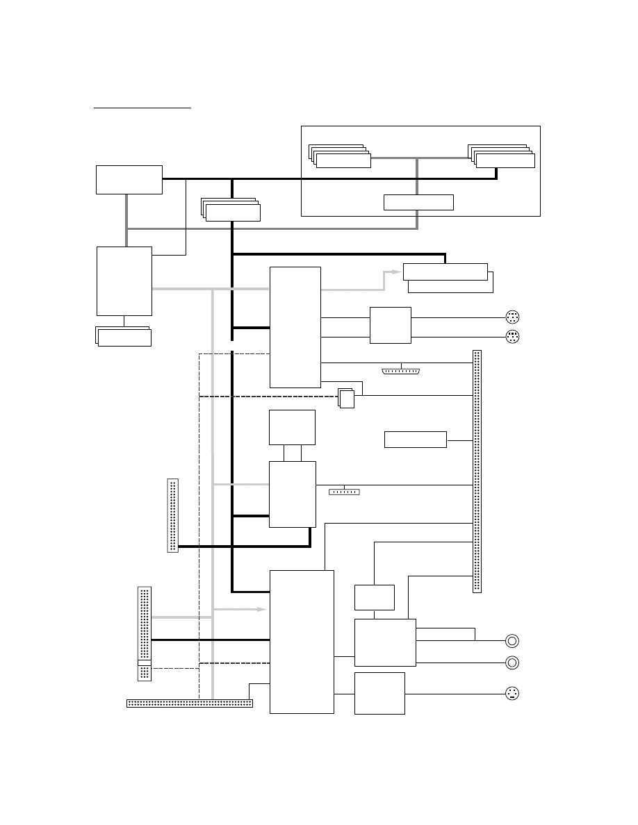
Block Diagram and Main ICs
2
The architecture of the Power Macintosh 5200 and 6200 computers is based on three
generations of microprocessors ; the MC68020/030, the MC68040, and the new
PowerPC 603. Figure 2-1 shows the system block diagram.
The internal bus structure consists of three internal buses; the 64-bit wide 603 data bus,
the 32-bit wde 68040 bus, and the 32-bit wide I/O bus. The 603 bus is connected directly
to the main processor and runs at the same clock rate. An external 256 KB second-level
cache and 4 MB of ROM attach directly to the 603 data bus and help to optomize system
performance.
The Capella custom IC provides the bus translation logic that bridges the 603 processor
and the 68040 based custom ICs. It translates the 64-bit data from the 603 data bus into
32-bit data required by the 68040 bus and provides the necessary signals to maintain
68040 protocol. Three custom ICs; F108, Valkyrie, and PrimeTime II connect directly to
the 68040 bus. The F108 custom IC provides memory control and bus arbitration logic,
the Valkyrie custom IC is the graphics display controller, and the PrimeTime II custom
IC controls most of the I/O functions.
The I/O bus is a 32-bit wide buffered bus that runs at 16 MHz and supports 68030 byte
steering and dynamic bus sizing. Although it is derived from the 68040 bus, it behaves
more like the 68030 interface to allow support for 68020 and 68030 expansion cards that
were designed for use in the Macintosh LC family of computers. The PrimeTime II
custom IC buffers the data portion of the I/O bus and provides a compatible interface
for I/O devices and software designed for use with the MC68030 miroprocessor.
Microprocessor
2
The Power Macintosh 5200 and 6200 computers use a PowerPC 603 microprocessor
running at 75 MHz. The principle features of the PowerPC 603 microprocessor include
■
full RISC processing architecture
■
parallel processing units: two integer and one floating-point
■
a branch manager that can usually implement branches by reloading the incoming
instruction queue without using any processing time
■
an internal memory management unit (MMU)
■
16 Kbyte of on-chip cache memory (8 Kbyte each for data and instructions)
For complete technical details, see the Motorola
PowerPC 603 RISC Microprocessor User’s
Manual.
This book is listed in “Supplementary Documents,” in the preface.
C H A P T E R 2
Architecture
Block Diagram and Main ICs
15
Figure 2-1
System Block diagram
Processor-
direct slot
68040 address bus
Apple
Desktop
Bus port
68040 Data bus
A31–0
Microphone
audio input
jack
Sound
output jack
D5–0
A31–0
D31–0
Serial
ports
D31–0
A31–0
DMD31–0
DMA8–0
Capella
Bus
translation
unit
RAM SIMM
RAM SIMM
RA11–0
Sound
amplifier
DFAC II
IOA1–0
A31–2
Communications slot
Drivers
and
receivers
Channel A
Channel B
Port A (modem)
Port B (printer)
SCSI CD
245 Buffer
IDE hard disk
Frame
buffer
1M DRAM
Valkyrie
DRAM
frame
buffer
controller
Video port
VID bus
Video-in
slot
IOA1–0
IOD31–16
F108
Memory
controller
bus
arbitrator
SCC
SCSI
IDE
IOD31–0
IOD31–0
PrimeTime II
Includes
SWIM II,
VIA1, VIA2,
sound
controller,
and
I/O bus
adapter
IOD31–0
A31–0
Floppy drive interface
Right channel
Left channel
CD inputs
Internal
chassis
connector
TV tuner board
SCSI connector
Cuda
ADB
real-time
clock/PRAM
Video mirror
connector
Tag RAM
D31–0
543 D latches
256 KB Cache
4 MB ROM
Transparent latch
LA21–5
P_A21–5
ROM/Cache DIMM card
LA21–5
LA17–5
P_A31–0
P_D4–0
P_D63–0
PPC 603
microprocessor

C H A P T E R 2
Architecture
16
Block Diagram and Main ICs
Second-Level Cache and ROM
2
The memory subsystem of the Power Macintosh 5200 and 6200 computers consists of
a 4 MB ROM and a 256 KB second-level (L2) cache, in addition to the internal cache
memory of the PowerPC 603 microprocessor. The ROM and the cache are contained on
the 160-pin ROM/Cache DIMM card that plugs into the main logic board. The Capella
custom IC provides burst mode control to the cache and ROM.
System RAM
2
The Power Macintosh 5200 and 6200 computers use two 72-pin SIMM socckets for
memory expansion. The computer is shipped with 8 MB installed in one of the SIMM
sockets and can be expanded to 64 MB. No soldered on-board memory is provided. The
SIMM sockets support both single- and double-sided DRAM modules. Using 4 Mbit
devices, each SIMM can be configured for 4 MB or 8 MB providing RAM expansion up
to 16 MB. Using 16 Mbit devices, you can configure each SIMM for 16 MB or 32 MB
providing RAM expansion up to 64 MB. The F 108 custom IC provides memory control
for the system RAM.
Custom ICs
2
The architecture of the Power Macintosh 5200 and 6200 computers is designed around
six large custom integrated circuits:
■
the Capella bus translation IC
■
the F108 memory controller and I/O support IC
■
the PrimeTime II I/O subsystem and buffer
■
the DFAC II sound input processor
■
the Cuda ADB controller
■
the Valkyrie video CLUT and DAC
The computer also uses several standard ICs that are used in other Macintosh
computers. This section describes only the custom ICs.
Capella IC
2
The Capella IC functions as the bridge between the PowerPC 603 microprocessor and the
the 68040 based circuits. It translates 64-bit data from the 603 data bus into 32-bit data
for the 68040 bus, and synchronizes arbitration between the two buses. The Capella IC
supports all combinations of 603 bus translation sizes and data alignment and provides
appropriate control signals for the 68040 bus. In addition, the Capella IC includes
registers that control the 256 KB L2 cache and the system ROM.

C H A P T E R 2
Architecture
Block Diagram and Main ICs
17
F108 IC
2
The F108 IC performs the system memory control functions. It also includes circuitry
equivalent to the SCC and SCSI controller ICs. The functional blocks in the F108 include
the following:
■
control logic for the system ROM and DRAM
■
SCSI controller
■
SCC serial I/O controller
■
IDE hard disk interface controller
The F108 IC is attached to the system 68040 bus and provides the control and timing
signals for the system ROM and RAM. The memory control logic supports byte, word,
longword, and line accesses to the system memory. If an access is not aligned to the
appropriate address boundary, that access requires multiple data transfers on the bus.
Note
The memory control logic in the F108 IC is the same as that in the F 108
IC used in the Power Macintosh Quadra 630 and LC 630.
◆
The SCSI controller in the F108 IC is just like an NCR 53C96. The PrimeTime II IC
provides the interface to the SCSI controller and also provides longword accumulation of
SCSI data for better performance. In the Power Macintosh 5200 and 6200 computers, the
clock signal to the SCSI controller is 18.75 MHz.
The SCC circuitry in the F108 IC is an 8-bit device just like the 8530 SCC. The
PCLK
signal to the SCC is an 8 MHz clock.
PrimeTime II IC
2
The PrimeTime II IC supports the I/O bus and functions as the bridge between the 68040
bus and the I/O bus. It combines functions performed by several ICs in previous
Macintosh designs. The PrimeTime II IC includes
■
data bus buffers for the internal I/O bus
■
address decoding for I/O devices
■
dynamic bus sizing and data routing for the I/O bus
■
interface adapters VIA1 and VIA2
■
interrupt controls
■
a SWIM II floppy disk controller
■
sound control logic and buffers
The PrimeTime II IC provides data bus features such as
byte steering,
which allows 8-bit
and 16-bit devices to be connected to a fixed byte lane, and
dynamic bus sizing,
which
allows software to read and write longwords to 8-bit and 16-bit devices. Those features
allow the computer to work with existing I/O software designed for the MC68030 and
MC68040.

C H A P T E R 2
Architecture
18
Block Diagram and Main ICs
The PrimeTime II IC also contains the sound control logic and the sound input and
output buffers. There are three separate buffers—one for sound input and two for stereo
sound output—so the computer can record sound input and process sound output
simultaneously.
DFAC II IC
2
The DFAC II custom IC is a digital filter audio chip that contains the sound input
processing devices. The DFAC II includes
■
input AGC comparators
■
antialias filtering
■
an A/D converter for input
■
a PWM converter for output
The DFAC II IC does not include the sound countrol logic and the input and output
buffers; those are part of the PrimeTime II IC.
For sound input, the DFAC II processes the signal from the sound input jack through a
sound input amplifier with automatic gain control, an input filter, an A/D converter, and
the necessary switching circuits. The DFAC II sends the resulting stream of digital sound
data to the PrimeTime II, which stores the data in its input buffer.
For sound output, circuits in the DFAC II take data from the sound output buffers and
generate stereo pulse-width-modulated (PWM) signals. The DFAC II merges the sound
playthrough signal with the PWM signals and sends the combined signals to an external
stereo PWM converter IC. After low-pass filtering in the PWM converter, the signals go
to the sound output jacks and to a separate amplifier for the built-in speaker. See the
section “Sound” beginning on page 32.
Cuda IC
2
The Cuda IC is a custom version of the Motorola MC68HC05 microcontroller. It provides
several system functions, including
■
the ADB interface
■
parameter RAM
■
the real-time clock
■
program control of the power supply (soft power)
■
the programming interface to devices on the IIC (inter-integrated circuit) bus
The devices on the IIC bus include the DFAC II sound IC, the digital video decoder and
scaler (DESC) on the video input module, and the Cyclops IC, which is the controller for
the remote control receiver. The computer reads and writes status and control informa-
tion to those devices by commands to the Cuda IC.

C H A P T E R 2
Architecture
Block Diagram and Main ICs
19
Valkyrie IC
2
The Valkyrie IC is a custom IC containing the logic for the video display. It includes the
following functions:
■
display memory controller
■
video CLUT (color lookup table)
■
video DAC (digital-to-analog converter)
A separate data bus handles data transfers between the Valkyrie IC and the display
memory. The display memory data bus is 32 bits wide, and all data transfers consist of 32
bits at a time. The Valkyrie IC breaks each 32-bit data transfer into several pixels of the
appropriate size for the current display mode—4, 8, or 16 bits per pixel. The Valkyrie IC
does not support 24 bits per pixel.
To keep up with the large amount of data that must be transferred into and out of the
display memory, the Valkyrie IC has several internal buffers. Besides input and output
buffers for display data, the Valkyrie IC also has a buffer for both addresses and data
being sent from the main processor to the display. That buffer can hold up to four
transactions, allowing the main processor to complete a write instruction to the display
memory and continue processing without waiting for some other transaction that might
be taking place on the display memory bus.
The CLUT in the Valkyrie custom IC provides color palettes for 4-bit and 8-bit display
modes.
In 16-bit display mode, the CLUT is used to provide gamma correction for the
stored color values. With a black-and-white or monochrome display mode, all three color
components (R, G, and B) are the same.
The Valkyrie IC uses several clocks. Its transactions with the CPU are synchronized
to the CPU_BCLK signal. Data transfers from the frame-buffer DRAM are clocked by
the MEM_CLK signal, which runs at 60 MHz. Data transfers to the CLUT and the
video output are clocked by the dot clock, which has a different rate for different
display monitors.
For more information about the interaction between the Valkyrie IC, the display
memory, and the main processor, see the section “Display RAM” later in this chapter.
Bus Arbitration
2
The system bus can support two bus masters, including the main processor and one I/O
bus master. The I/O master has higher priority. Either bus master can park on the bus as
long as no higher priority master requests the bus.
The bus request from the I/O bus master is initiated by the PrimeTime II IC and comes
from one of two sources: the PDS expansion card or the communications card. Devices
on those cards are not connected directly to the system bus; they arbitrate the bus by
way of the I/O bus and the PrimeTime II IC. See the section “Bus Master on a Card”
beginning on page 56.

C H A P T E R 2
Architecture
20
Block Diagram and Main ICs
The Capella IC synchronizes the bus arbitration between the 603 bus and the 68040 bus.
The PowerPC 603 microprocessor is the default bus master. The Capella IC gains access
to the 68040 bus when the I/O master is granted to the bus. The PowerPC 603 micro-
processor continues to execute instructions from the ROM and the L2 cache during bus
arbitration resulting in improved system performance.
Display RAM
2
The display memory in the Power Macintosh 5200 and 6200 computers is separate from
the main memory. To reduce the cost of the computer, the display memory is imple-
mented with DRAM devices instead of more expensive VRAM devices. The display
memory consists of 1 MB of 60 ns DRAM devices configured to make a 32-bit data bus.
The display memory cannot be expanded.
The display memory contains three separate frame buffers. The first frame buffer holds
the graphics data—the display that is generated by the computer. The other two frame
buffers hold video data from the video input module. The video data frame buffers are
used alternately: while one is supplying data to be sent to the video monitor, the other is
receiving the next frame of video input.
The display data generated by the computer can have pixel depths of 4, 8, or 16 bits for
monitors up to 64-by-480 pixels and 4 or 8 bits for larger monitors and the 800-by-600-pixel
display on a multiscan monitor. Data from the video input module is always stored and
transferred at 16 bits per pixel. The video frame buffers support live video in a
320-by-240-pixel frame at 30 frames per second.
Note
The Power Macintosh 5200 and 6200 computers cannot display live
video from the video-in module on monitor sizes larger than 800-by-
600 pixels. Apple does not recommend the use of such monitors with
these computers.
◆
The Power Macintosh 5200 and 6200 computers can display video in a window inside
the computer graphics display. The Valkyrie IC has registers that contain the starting
location of the video window within the display, the starting address of the video data
in the video buffer, and the size of the video window.
Note
Because the Power Macintosh 5200 and 6200 computers operate only in
32-bit addressing mode, they do not support the Apple IIe Card for the
Macintosh LC.
◆

C H A P T E R 2
Architecture
Address Map
21
Address Map
2
The Power Macintosh 5200 and 6200 computers support only 32-bit addressing.
Figure 2-2 on page 22 shows a simplified address map.
Note
Developers should not use actual hardware addresses in applications;
they should always communicate with hardware devices by means of
system software.
◆
RAM Addresses
2
The first 1 GB of the address space is reserved for RAM. The actual amount of RAM
installed can be from 8 MB to 64 MB. At startup time, a routine in the ROM determines
the amount of RAM available and stores the size in a low-memory global variable.
Display RAM Addresses
2
The Power Macintosh 5200 and 6200 computers use separate DRAM to store the display
buffers. The display RAM occupies dedicated address space starting at $F900 0000, as
shown in Figure 2-2 on page 22.
Addresses for PDS Expansion Cards
2
The PDS expansion card uses address space from $FE00 0000 to $FFFF FFFF, corre-
sponding to NuBus
slot $E, and from $E000 0000 to $EFFF FFFF, corresponding
to NuBus Super Slot $E. For more information, see the section “Card Address Space”
on page 58.

C H A P T E R 2
Architecture
22
Address Map
Figure 2-2
Simplified address map
$FF00 0000
$FFFF FFFF
$F980 0000
$7000 0000
$53FF FFFF
$0000 0000
$0400 0000
$5000 0000
$6000 0000
$4FFF FFFF
$FE00 0000
Expansion slot
ROM image
040 ROM space
Expansion
super
slot
space
I/O
$F000 0000
$F900 0000
Display RAM
603 ROM space
$4000 0000
RAM space

C H A P T E R 3
I/O Features
3
Figure 3-0
Listing 3-0
Table 3-0
C H A P T E R 3
I/O Features
24
Serial I/O Ports
This chapter describes both the built-in I/O devices and the interfaces for external I/O
devices. It also describes the types of external video monitors that can be used with the
Power Macintosh 5200 and 6200 computers.
Serial I/O Ports
3
The Power Macintosh 5200 and 6200 computers have two serial ports, one for a printer
and one for a modem. Both serial ports have 9-pin mini-DIN sockets that accept either
8-pin or 9-pin plugs.
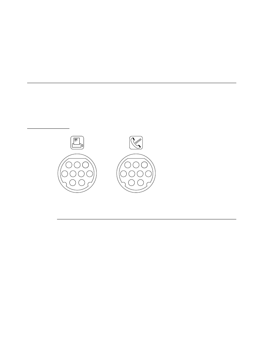
Figure 3-1 shows the mechanical arrangement of the pins on the
serial port sockets; Table 3-1 shows the signal assignments.
Figure 3-1
Serial port sockets
Table 3-1
Serial port signals
Pin
number
Signal description
1
Handshake output
2
Handshake input
3
Transmit data –
4
Ground
5
Receive data –
6
Transmit data +
7
General-purpose input
8
Receive data +
9
+5 volts
Printer
Modem
8
7
1
5
4
2
3
9
6
8
7
1
5
4
2
3
9
6

C H A P T E R 3
I/O Features
ADB Port
25
Pin 9 on each serial connector provides +5 V power from the ADB power supply. An
external device should draw no more than 100 mA from that pin. The total current
available for all devices connected to the +5 V supply for the ADB and the serial ports is
500 mA. Excessive current drain will cause a fuse to interrupt the +5 V supply; the fuse
automatically resets when the load returns to normal.
Both serial ports include the GPi (general-purpose input) signal on pin 7. The GPi signal
for each port connects to the corresponding data carrier detect input on the SCC portion
of the F108 custom IC, described in Chapter 2. On serial port A (the modem port), the
GPi line can be connected to the receive/transmit clock (RTxCA) signal on the SCC. That
connection supports devices that provide separate transmit and receive data clocks, such
as synchronous modems. For more information about the serial ports, see
Guide to the
Macintosh Family Hardware,
second edition.
ADB Port
3
The Apple Desktop Bus (ADB) port on the Power Macintosh 5200 and 6200 computers is
functionally the same as on other Macintosh computers.
The ADB is a single-master, multiple-slave serial communications bus that uses an
asynchronous protocol and connects keyboards, graphics tablets, mouse devices, and
other devices to the computer. The custom ADB microcontroller drives the bus and reads
status from the selected external device. A 4-pin mini-DIN connector connects the ADB
to the external devices. Table 3-2 lists the ADB connector pin assignments. For more
information about the ADB, see
Guide to the Macintosh Family Hardware,
second edition.
Note
The total current available for all devices connected to the +5V pins on
the ADB and the modem port is 500 mA. Each device should use no
more than 100 mA.
◆
Table 3-2
ADB connector pin assignments
Pin
number
Name
Description
1
ADB
Bidirectional data bus used for input and output. It is
an open-collector signal pulled up to +5 volts through
a 470-ohm resistor on the main logic board.
2
PSW
Power-on signal that generates reset and interrupt key
combinations.
3
+5V
+5 volts from the computer.
4
GND
Ground from the computer.

C H A P T E R 3
I/O Features
26
Floppy Disk Drive
Floppy Disk Drive
3
The Power Macintosh 5200 and 6200 computers have one internal high-density floppy
disk drive (Apple SuperDrive). The drive is connected to a 20-pin connector on a cable
that is connected to the main logic board by the internal chassis connector. Table 3-3
shows the pin assignments on the floppy disk connector.
Table 3-3
Pin assignments on the floppy disk connector
Pin
number
Signal name
Signal description
1
GND
Ground
2
PH0
Phase 0: state control line
3
GND
Ground
4
PH1
Phase 1: state control line
5
GND
Ground
6
PH2
Phase 2: state control line
7
GND
Ground
8
PH3
Phase 3: register write strobe
9
n.c.
Not connected
10
/WRREQ
Write data request
11
+5V
+5 volts
12
SEL
Head select
13
+12V
+12 volts
14
/ENBL
Drive enable
15
+12V
+12 volts
16
RD
Read data
17
+12V
+12 volts
18
WR
Write data
19
+12V
+12 volts
20
n.c.
Not connected

C H A P T E R 3
I/O Features
IDE Hard Disk
27
IDE Hard Disk
3
The Power Macintosh 5200 and 6200 computers have an internal hard disk that uses the
standard IDE interface. This interface, used for IDE drives on IBM AT–compatible
computers, is also referred to as the ATA interface. The implementation of the ATA inter-
face on the Power Macintosh 5200 and 6200 computers is a subset of the ATA interface
specification, ANSI proposal X3T9.2/90-143, Revision 3.1.
Hard Disk Specifications
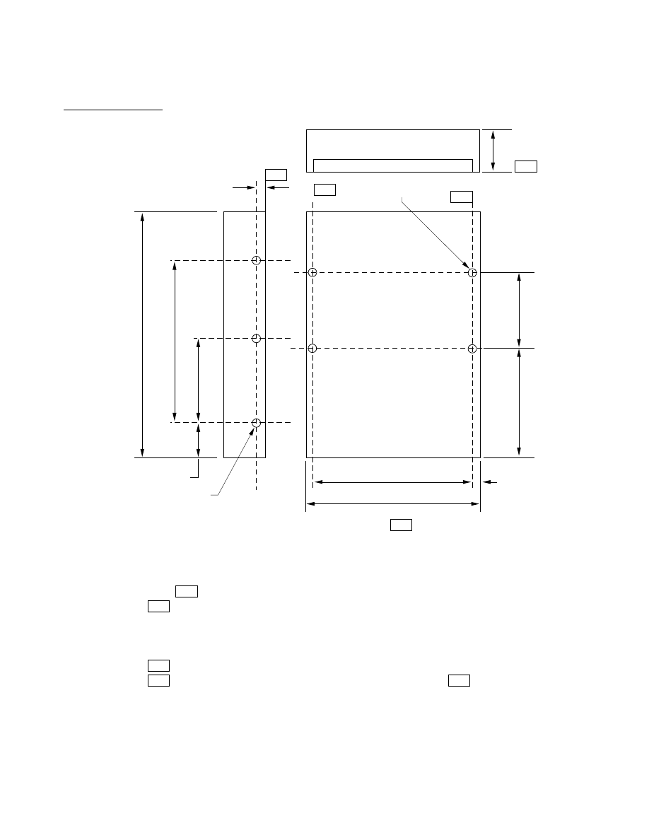
3
Figure 3-2 on page 28 shows the maximum dimensions of the hard disk and the location
of the mounting holes. As the figure shows, the minimum clearance between conductive
components and the bottom of the mounting envelope is 0.5 mm.
Hard Disk Connectors
3
The internal hard disk has a standard 40-pin IDE connector and a separate 4-pin power
connector. The 40-pin connector cable is part of the cable harness attached to the main
logic board by the internal chassis connector, as shown in Figure 2-1 on page 15. The
power cable is attached directly to the power supply.
The exact locations of the IDE connector and the power connector are not specified, but
the relative positions must be as shown in Figure 3-2 on page 28 so that the cables and
connectors will fit.
C H A P T E R 3
I/O Features
28
IDE Hard Disk
Figure 3-2
Maximum dimensions of the hard disk
6.40 (.252)2x
3
IDE connector
Power
Mounting hole 6-32, .22"
min. full thread, 4X
A
B
A
7
101.6 (4.00)
95.25 (3.75)
3.20 (.125) 2x
60.30 (2.37)
44.40 (1.75)
60.00 (2.36) 2x
101.6 (4.00) 2x
146.0 (5.75)
25.4 (1.00)
16.00 (.63) 2x
Mounting hole
6-32, through 6x
Notes:
1
2
3
4
5
6
7
8
A Defined by plane of bottom mount holes
B Defined by center line of bottom mount holes
40-pin IDE and 4-pin power connector placement must not be reversed
All dimensions in MM (inch)
Drawing not to scale
Tolerances .X = +
0.50, .XX = +
0.25
Dimension to be measured at center line of side-mount holes
Minimum 0.5 MM clearance from any conductive PCB components to A
–
–

C H A P T E R 3
I/O Features
IDE Hard Disk
29
Pin Assignments
3
Table 3-4 shows the pin assignments on the 40-pin IDE hard disk connector. A slash (/)
at the beginning of a signal name indicates an active-low signal.
Note
The IDE data bus is connected to the I/O bus through bidirectional bus
buffers. To match the big-endian format of the MC68030-compatible bus,
the bytes are swapped. The lower byte of the IDE data bus, DD(0–7), is
connected to the high byte of the upper word of the I/O bus, IOD(24–31).
The higher byte of the IDE data bus, DD(8–15), is connected to the low
byte of the upper word of the I/O bus, IOD(16–23).
◆
Table 3-4
Pin assignments on the IDE hard disk connector
Pin
number
Signal name
Pin
number
Signal name
1
/RESET
2
GROUND
3
DD7
4
DD8
5
DD6
6
DD9
7
DD5
8
DD10
9
DD4
10
DD11
11
DD3
12
DD12
13
DD2
14
DD13
15
DD1
16
DD14
17
DD0
18
DD15
19
GROUND
20
KEY
21
Reserved
22
GROUND
23
DIOW
24
GROUND
25
DIOR
26
GROUND
27
/IORDY
28
Reserved
29
Reserved
30
GROUND
31
INTRQ
32
/IOCS16
33
DA1
34
/PDIAG
35
DA0
36
DA2
37
/CS0
38
/CS1
39
/DASP
40
GROUND

C H A P T E R 3
I/O Features
30
SCSI Bus
IDE Signal Descriptions
3
Table 3-5 describes the signals on the IDE hard disk connector.
SCSI Bus
3
The Power Macintosh 5200 and 6200 computers have a SCSI bus for an optional internal
CD-ROM device and one or more external SCSI devices. The CD-ROM device receives
power directly from the power supply.
Table 3-5
Signals on the IDE hard disk connector
Signal name
Signal description
DA(0–2)
IDE device address; used by the computer to select one of the
registers in the IDE drive. For more information, see the
descriptions of the CS0 and CS1 signals.
DD(0–15)
IDE data bus; buffered from IOD(16–31) of the computer’s I/O
bus. DD(0–15) are used to transfer 16-bit data to and from the
drive buffer. DD(8–15) are used to transfer data to and from
the internal registers of the drive, with DD(0–7) driven high
when writing.
CS0
IDE register select signal. It is asserted high to select the
additional control and status registers on the IDE drive.
CS1
IDE register select signal. It is asserted high to select the main
task file registers. The task file registers indicate the command,
the sector address, and the sector count.
/IORDY
IDE I/O ready; when driven low by the drive, signals the CPU
to insert wait states into the I/O read or write cycles.
/IOCS16
IDE I/O channel select; asserted low for an access to the data
port. The computer uses this signal to indicate a 16-bit data
transfer.
/DIOR
IDE I/O data read strobe.
/DIOW
IDE I/O data write strobe.
INTRQ
IDE interrupt request. This active high signal is used to inform
the computer that a data transfer is requested or that a
command has terminated.
/RESET
Hardware reset to the drive; an active low signal.
Key
This pin is the key for the connector.

C H A P T E R 3
I/O Features
SCSI Bus
31
SCSI Connectors
3
The SCSI connector for the internal CD-ROM drive is a 50-pin connector with the
standard SCSI pin assignments. It attaches to a cable that is connected to the main logic
board by the internal chassis connector. The external SCSI connector is a 25-pin D-type
connector with the same pin assignments as other Apple SCSI devices. Table 3-6 shows
the pin assignments on the internal and external SCSI connectors.
Table 3-6
Pin assignments for the SCSI connectors
Pin number
(internal 50-pin)
Pin number
(external 25-pin)
Signal name
Signal description
2
8
/DB0
Bit 0 of SCSI data bus
4
21
/DB1
Bit 1 of SCSI data bus
6
22
/DB2
Bit 2 of SCSI data bus
8
10
/DB3
Bit 3 of SCSI data bus
10
23
/DB4
Bit 4 of SCSI data bus
12
11
/DB5
Bit 5 of SCSI data bus
14
12
/DB6
Bit 6 of SCSI data bus
16
13
/DB7
Bit 7 of SCSI data bus
18
20
/DBP
Parity bit of SCSI data bus
25
–
n.c. Not
connected
26
25
TPWR
+5 V terminator power
32
17
/ATN
Attention
36
6
/BSY
Bus busy
38
5
/ACK
Handshake acknowledge
40
4
/RST
Bus reset
42
2
/MSG
Message phase
44
19
/SEL
Select
46
15
/C/D
Control or data
48
1
/REQ
Handshake request
50
3
/I/O
Input or output
20, 22, 24, 28,
30, 34, and
all odd pins
except pin 25
7, 9, 14, 16, 18,
and 24
GND
Ground

C H A P T E R 3
I/O Features
32
Sound
SCSI Bus Termination
3
The internal end of the SCSI bus is terminated by a 220/330 passive terminator. The
terminator is located on the main logic board near the portion of the internal chassis
connector that contains the signals for the internal CD-ROM drive. The internal
CD-ROM drive does not include a terminator.
Sound
3
The sound system supports 8-bit stereo sound output and monaural sound input. Like
other Macintosh computers, the Power Macintosh 5200 and 6200 computers can create
sounds digitally and play the sounds through their internal speakers or send the sound
signals out through the sound output jacks. They can also record sound from several
sources: the built-in microphone, a microphone connected to the sound input jack, the
video input module, or a compact disc in the CD-ROM player.
Sound Output
3
The Power Macintosh 5200 and 6200 computers have two built-in speakers and two
sound output jacks, one on the front and one on the back. Both output jacks are
connected to the sound amplifier; the jack on the front is intended for ease of access
when connected to a pair of headphones. Inserting a plug into either jack disconnects the
internal speakers.
Sound output is controlled by the PrimeTime II IC. A 8-bit data stream from the
PrimeTime II IC is converted to an analog signal and level shifted before entering the
DFAC II IC for further filtering and mixing. The DFAC II IC provides the stereo sound
output to both the internal speakers and the sound output jacks.
Sound Input
3
The Power Macintosh 5200 and 6200 computers have a sound input jack on the back
for connecting an external microphone or other sound source. The sound input jack
accepts a standard 1/8-inch phone plug, either monophonic or stereophonic (two signals
plus ground).
The sound input jack accepts either the Apple
PlainTalk line-level microphone or a pair
of line-level signals by way of a separate adapter. The internal circuitry mixes the
stereophonic signals into a monophonic signal for digitization.
Note
The Apple PlainTalk microphone requires power from the main
computer, which it obtains by way of an extra-long, 4-conductor plug
that makes contact with a 5-volt pin inside the sound input jack.
◆

C H A P T E R 3
I/O Features
Sound
33
IMPORTANT
The microphone for the Macintosh LC and LC II does not work with the
Power Macintosh 5200 and 6200 computers; they require the line-level
signal provided by the Apple PlainTalk microphone.
▲
Sound Input Specifications
3
The sound input jack has the following electrical characteristics:
■
Input impedance: 100k ohms
■
Average line level: 100 mV RMS
■
Average microphone level: 70 mV RMS
■
Maximum input level: 1.8 V RMS
Routing of the Sound Signals
3
Sound input signals can be routed in two ways: they can be recorded (digitized) or
they can be sent directly to the sound outputs and speakers, bypassing the sound IC.
Table 3-7 lists the sound sources and shows how each one can be routed.
Digitizing Sound
3
The Power Macintosh 5200 and 6200 computers digitize and record sound as 8-bit
samples. They can use either of two sampling rates: 11k samples per second and 22k
samples per second. The sound circuits include input and output filters with switchable
cutoff (–3 dB) frequencies that correspond to the two sampling rates: 3.5 kHz cutoff for
the 11k sampling rate and 7 kHz cutoff for the 22k sampling rate.
The sound system always plays samples at the 22k sampling rate; when playing samples
recorded at the 11k sampling rate, the software writes each sample to the sound
buffer twice.
Table 3-7
Sound sources and routing
Sound source
Record
Bypass
Sound input jack
√
–
Modem
√
–
CD-ROM player
√
√
Video sound (video input module)
√
√

C H A P T E R 3
I/O Features
34
Keyboard
Sound Modes
3
The sound mode is selected by a call to the Sound Manager. The sound circuitry
normally operates in one of three modes:
■
Sound playback: computer-generated sound is sent to the speaker and the sound
output jacks.
■
Sound playback with playthrough: computer sound and sound input are mixed and
sent to the speaker and the sound output jacks.
■
Sound record with playthrough: input sound is recorded and also fed through to the
speaker and the sound output jacks.
When recording from a microphone, applications should reduce the playthrough volume
to prevent possible feedback from the speaker to the microphone.
The PrimeTime III IC provides separate sound buffers for input and for stereo output, so
the computer can record and send digitized sound to the sound outputs simultaneously.
Keyboard
3
The keyboard has a Power key, identified by the symbol
p
. When the user chooses Shut
Down from the Special menu, the computer either shuts down or a dialog appears
asking if you really want to shut down. The user can also turn off the power by pressing
the Power key .
There are no programmer’s switches, so the user invokes the reset and NMI functions by
pressing Command key combinations while holding down the Power key, as shown in
Table 3-8. The Command key is identified by the symbols
ð
and
x
.
Note
The user must hold down a key combination for at least 1 second to
allow the ADB microcontroller enough time to respond to the NMI or
hard-reset signal.
◆
Note
The NMI function can always be activated from the keyboard. This is a
change from the Macintosh LC computer, where keyboard activation of
the NMI function can be disabled by the software.
◆
Table 3-8
Reset and NMI key combinations
Key combination
Function
Command-Power (
x
-
p
)
NMI (always active)
Control-Command-Power (Control-
x
-
p
)
Reset

C H A P T E R 3
I/O Features
Video
35
Video
3
The main difference between the Power Macintosh 5200 and the Power Macintosh 6200,
computers, other than physical appearence, is the way in which they display video
information. The Power Macintosh 5200 computer has a built-in 15-inch multiscan
monitor whereas the Power Macintosh 6200 computer requires an external monitor.
Bothconfigurations support pixel display sizes of 512
×
384, 640
×
480, 800
×
600, and
824
×
632. When power is applied, the monitor is initially set for a display size of
640
×
480 pixels. The user can switch the monitor resolution on the fly from the
computer’s Control Panels menu.
Optional Video Display Mirror Output Feature
3
The Power Macintosh 5200 uses a feature, called video display mirror output, to make
the video information on its built-in monitor available to an external monitor. This
means that the information displayed on an external monitor is a mirror image of that
displayed on the built-in monitor. This feature is implemented by plugging an optional
video buffer board into the 22-pin Video Mirror connector on the main logic board. The
Video Mirror connector’s pin assignments are shown in Table 3-9.
The optional video buffer board includes a ribbon cable with a DB-15 connector. This
connector attaches to a large opening in the upper part of the computer’s back panel,
identified in Figure 1-2 on page 6, as the Monitor Out port. The cable from an external
video monitor plugs into this DB-15 connector to allow the external monitor to display a
mirror image of the video on the built-in monitor.
Table 3-9
Video mirror connector pin assignments
Pin
Signal name
Description
1
VID GND
Video ground
2
RED
Red signal
3
GREEN
Green signal
4
VID GND
Video ground
5
VID GND
Video ground
6
BLUE
Blue signal
7
CSYNC
C sync
8
VSYNC
Vertical sync
9
MLB.SYNC.EN.L
Not used (reserved)
10
HSYNC
Horizontal sync
continued

C H A P T E R 3
I/O Features
36
Video
External Video Monitors
3
The computers can work with several sizes of external video monitors, however, you can
connect an external monitor to the Power Macintosh 5200 only if the optional video
display mirror out feature is implemented on that computer, and then it can only display
the same video as the internal monitor. Table 3-12 shows the monitor types supported
and the maximum pixel depths available. The pixel depth determines the maximum
number of colors that can be displayed. The maximum pixel depth available depends on
the size of the monitor’s screen.
For more information about the video monitors, see “Video Timing Parameters” on
page 38.
*
The Power Macintosh 5200 computer does not support screen sizes of 512 by 384 pixels.
11
DAC.ISET.1
Not used(reserved)
12
DAC.ISET.2
Not used (reserved)
13
SND GND
Not used (reserved)
14
SND RIGHT
Not used (reserved)
15
SND LEFT
Not used (reserved)
16
+5V
+ 5 volts
17
GND
Ground
18
SDAT
Not used (reserved)
19
SCLK
Not used (reserved)
20
+12V
+12 volts
21
–12V
–12 volts
22
Dot Clock
Scaled dot clock (scaled to 10%)
Table 3-10
Maximum pixel depths for video monitors
Monitor type
Screen size,
in pixels
Maximum pixel
depth, in bits
per pixel
Maximum number
of colors displayed
12-inch color
*
512 by 384
16
32,768
14-inch color
640 by 480
16
32,768
15-inch multiscan
800 by 600
8
256
VGA
640 by 480
8
256
SVGA
800 by 600
8
256
16-inch color
832 by 624
8
256
Table 3-9
Video mirror connector pin assignments (continued)
Pin
Signal name
Description

C H A P T E R 3
I/O Features
Video
37
External Video Connection for Power Macintosh 6200
3
The Power Macintosh 6200 computer requires an external monitor. The cable from the
external monitor plugs into a standard DB-15 video port on the upper right part of the
enclosure’s rear panel. This connector is not available on the Power Macintosh 5200, which
uses the video mirror display output option for external video. The pin assignments for
the external video connector on the Power Macintosh 6200 are shown in Table 3-11.
Table 3-11
Pin assignments for external video connector
Pin
number
Signal name
Description
1
RED.GND
Red video ground
2
RED.VID
Red video signal
3
/CSYNC
Composite synchronization signal
4
SENSE0
Monitor sense signal 0
5
GRN.VID
Green video signal
6
GRN.GND
Green video ground
7
SENSE1
Monitor sense signal 1
9
BLU.VID
Blue video signal
10
SENSE2
Monitor sense signal 2
11
GND
CSYNC and VSYNC ground
12
/VSYNC
Vertical synchronization signal
13
BLU.GND
Blue video ground
14
HSYNC.GND
HSYNC ground
15
/HSYNC
Horizontal synchronization signal
Shell
SGND
Shield ground

C H A P T E R 3
I/O Features
38
Video Timing Parameters
Video Timing Parameters
3
The computers support several different types of monitors and screen sizes, as listed in
Table 3-12.
Figure 3-3 shows simplified timing diagrams and identifies the horizontal and vertical
timing parameters in a video signal. Table 3-13 and Table 3-13 list the values of those
parameters for the different types of monitors.
Table 3-12
Monitors supported
Monitor type
Screen size (pixels)
12-inch color
512 by 384
14-inch color
640 by 480
15-inch multiscan
800 by 600
VGA
640 by 480
SVGA
800 by 600
16-inch color
832 by 624
C H A P T E R 3
I/O Features
Video Timing Parameters
39
Figure 3-3
Video timing diagram
Video
H sync space
H image space
H line length
H back porch
H sync pulse
H front porch
HBLANK
/HSYNC
Black
Horizontal timing
Video
V sync space
V image space
V line length
V back porch
V sync pulse
V front porch
VBLANK
/VSYNC
Vertical timing
White
Black
White

C H A P T E R 3
I/O Features
40
Video Timing Parameters
Table 3-13 lists the timing parameters for the smaller monitors listed: the 12-inch color
monitor, the 14-inch color monitor, and a standard VGA monitor.
Table 3-13
Video timing parameters for smaller monitors
Parameter
Monitor type and dimensions
12-inch color
(512 by 384)
14-inch color
(640 by 480)
VGA
(640 by 480)
Dot clock
15.67 MHz
30.24 MHz
25.18 MHz
Dot time
63.83 ns
33.07 ns
39.72 ns
Line rate
24.48 kHz
35.00 kHz
31.47 kHz
Line time
40.85
µ
s
(640 dots)
28.57
µ
s
(864 dots)
31.78
µ
s
(800 dots)
Horizontal active
video
512 dots
640 dots
640 dots
Horizontal blanking
128 dots
224 dots
160 dots
Horizontal front
porch
16 dots
64 dots
16 dots
Horizontal sync
pulse
32 dots
64 dots
96 dots
Horizontal back
porch
80 dots
96 dots
48 dots
Frame rate
60.15 Hz
66.72 Hz
59.94 Hz
Frame time
16.63 ms
(407 lines)
15.01 ms
(525 lines)
16.68 ms
(525 lines)
Vertical active video
384 lines
480 lines
480 lines
Vertical blanking
23 lines
45 lines
45 lines
Vertical front porch
1 line
3 lines
10 lines
Vertical sync pulse
3 lines
3 lines
2 lines
Vertical back porch
19 lines
39 lines
33 lines

C H A P T E R 3
I/O Features
Video Timing Parameters
41
Table 3-14 lists the timing parameters for SVGA monitors running at 60 and 72 frames
per second, and for the 16-inch color monitor.
Table 3-14
Video timing parameters for larger monitors
Parameter
Monitor type and dimensions
SVGA (800 by 600
at 60 frames/sec)
SVGA (800 by 600
at 72 frames/sec)
16-inch color
(832 x 624)
Dot clock
40.00 MHz
50.00 MHz
57.2832 MHz
Dot time
25.00 ns
20.00 ns
17.46 ns
Line rate
37.88 kHz
48.08 kHz
49.725 kHz
Line time
26.4
µ
s
(1056 dots)
20.80
µ
s
(1040 dots)
20.11
µ
s
(1152 dots)
Horizontal active
video
800 dots
800 dots
832 dots
Horizontal
blanking
256 dots
240 dots
320 dots
Horizontal front
porch
40 dots
56 dots
32 dots
Horizontal sync
pulse
128 dots
120 dots
64 dots
Horizontal back
porch
88 dots
64 dots
224 dots
Frame rate
60.31 Hz
72.18 Hz
74.55 Hz
Frame time
16.58 ms
(628 lines)
13.85 ms
(666 lines)
13.41 ms
(667 lines)
Vertical active
video
600 lines
600 lines
624 lines
Vertical blanking
28 lines
66 lines
43 lines
Vertical front porch
1 line
37 lines
1 line
Vertical sync pulse
4 lines
6 lines
3 lines
Vertical back porch
23 lines
23 lines
39 lines


C H A P T E R 4
Expansion Features
4
Figure 4-0
Listing 4-0
Table 4-0

C H A P T E R 4
Expansion Features
44
RAM Expansion
This chapter describes the expansion features of the Power Macintosh 5200 and 6200
computers: the RAM expansion slot, the I/O expansion slot, the DVA connector on the
video input module, and the Communications slot.
Note
Apple does not support development of third-party
cards for the video input slot.
◆
RAM Expansion
4
The computers come with 8 MB of system RAM installed in one of two 72-pin SIMMs on
the main logic board. The user can expand the RAM up to a maximum of 64 MB by
plugging in different SIMM configurations into the SIMM sockets.
Note
The video display buffer uses separate on-board DRAM.
The display DRAM cannot be expanded.
◆
RAM Configurations
4
Table 4-1 shows the RAM configurations for different amounts of RAM. For more
information, see the section “RAM Addresses” on page 21.
Table 4-1
RAM configurations
SIMM 1
SIMM 2
Maximum DRAM
8 MB
0 MB
8 MB
8 MB
4 MB
12 MB
8 MB
8 MB
16 MB
16 MB
4 MB
20 MB
16 MB
8 MB
24 MB
16 MB
16 MB
32 MB
32 MB
4 MB
36 MB
32 MB
8 MB
40 MB
32 MB
16 MB
48 MB
32 MB
32 MB
64 MB

C H A P T E R 4
Expansion Features
RAM Expansion
45
Signals on the RAM SIMM Slot
4
Table 4-2 gives the signal assignments for the pins of the RAM SIMM slot.
IMPORTANT
RAM SIMMs used in Macintosh computers must meet the timing and
electrical standards of those machines. SIMMs designed for other
computers may not work.
▲
Table 4-2
Signal assignments on the RAM SIMM slot
Pin
Signal name
Description
1
GND
Ground
2
DQ0
Data input/output bus, bit 0
3
DQ16
Data input/output bus, bit 16
4
DQ1
Data input/output bus, bit 1
5
DQ17
Data input/output bus, bit 17
6
DQ2
Data input/output bus, bit 2
7
DQ18
Data input/output bus, bit 18
8
DQ3
Data input/output bus, bit 3
9
DQ19
Data input/output bus, bit 19
10
+5V
+5 volts
11
n.c.
Not connected
12
A0
Address bus, bit 0
13
A1
Address bus, bit 1
14
A2
Address bus, bit 2
15
A3
Address bus, bit 3
16
A4
Address bus, bit 4
17
A5
Address bus, bit 5
18
A6
Address bus, bit 6
19
A10
Address bus, bit 10
20
DQ4
Data input/output bus, bit 4
21
DQ20
Data input/output bus, bit 20
22
DQ5
Data input/output bus, bit 5
23
DQ21
Data input/output bus, bit 21
24
DQ6
Data input/output bus, bit 6
continued

C H A P T E R 4
Expansion Features
46
RAM Expansion
25
DQ22
Data input/output bus, bit 22
26
DQ7
Data input/output bus, bit 7
27
DQ23
Data input/output bus, bit 23
28
A7
Address bus, bit 7
29
A11
Address bus, bit 11
30
+5V
+5 volts
31
A8
Address bus, bit 8
32
A9
Address bus, bit 9
33
/RAS3
Row address strobe 3
34
/RAS2
Row address strobe 2
35
—
Reserved
36
—
Reserved
37
—
Reserved
38
—
Reserved
39
GND
Ground
40
/CAS0
Column address strobe 0
41
/CAS2
Column address strobe 2
42
/CAS3
Column address strobe 3
43
/CAS1
Column address strobe 1
44
/RAS0
Row address strobe 0
45
/RAS1
Row address strobe 1
46
n.c.
Not connected
47
/W
Write enable
48
n.c.
Not connected
49
DQ8
Data input/output bus, bit 8
50
DQ24
Data input/output bus, bit 24
51
DQ9
Data input/output bus, bit 9
52
DQ25
Data input/output bus, bit 25
53
DQ10
Data input/output bus, bit 10
54
DQ26
Data input/output bus, bit 26
55
DQ11
Data input/output bus, bit 11
continued
Table 4-2
Signal assignments on the RAM SIMM slot (continued)
Pin
Signal name
Description

C H A P T E R 4
Expansion Features
RAM Expansion
47
RAM Devices
4
The RAM controller in the F108 IC supports 1 Mbit, 4 Mbit, and 16 Mbit devices; it does
not support 64 Mbit devices. The RAM controller supports four banks of RAM.
Each RAM SIMM can support either one or two banks. A one-bank SIMM using 1 Mbit,
4 Mbit, or 16 Mbit devices provides RAM expansion of 1 MB, 4 MB, or 16 MB,
respectively. A two-bank SIMM using the same devices provides 2 MB, 8 MB, or 32 MB.
IMPORTANT
You should not use 1-bit-wide DRAM devices in a RAM SIMM because
the required number of devices adds excessive capacitive loading to the
address and control buses.
▲
The access time of the DRAM devices must be 80 ns or less. The RAM controller in the
F108 IC performs the refresh function, using CAS before RAS refresh and refreshing the
DRAM devices within 15.6
µ
s. DRAM devices that require refreshing within 7.8
µ
s are
not supported.
The RAM controller in the F108 IC supports line burst transfers but does not support
interleaved accesses.
56
DQ27
Data input/output bus, bit 27
57
DQ12
Data input/output bus, bit 12
58
DQ28
Data input/output bus, bit 28
59
+5V
+5 volts
60
DQ29
Data input/output bus, bit 29
61
DQ13
Data input/output bus, bit 13
62
DQ30
Data input/output bus, bit 30
63
DQ14
Data input/output bus, bit 14
64
DQ31
Data input/output bus, bit 31
65
DQ15
Data input/output bus, bit 15
66
n.c.
Not connected
67
—
Reserved
68
—
Reserved
69
—
Reserved
70
—
Reserved
71
n.c.
Not connected
72
GND
Ground
Table 4-2
Signal assignments on the RAM SIMM slot (continued)
Pin
Signal name
Description

C H A P T E R 4
Expansion Features
48
RAM Expansion
Addressing RAM
4
Signals A[0–11] make up a 12-bit multiplexed address bus that can support several
different types of DRAM devices.
Depending on their internal design and size, different types of DRAM devices require
different row and column address multiplexing. The F108 custom IC provides for two
addressing modes, selected individually for each bank of DRAM. The system software
initializes the address mode bits as part of the process of determining the amount of
RAM installed in the computer.
Table 4-3 shows how the signals are multiplexed during the row and column address
phases for each of the addressing modes.
Table 4-4 shows the address modes used with several types of DRAM devices. The
devices are characterized by their bit dimensions: for example, a 256K by 4-bit device
has 256 addresses and stores 4 bits at a time.
Table 4-3
Address multiplexing for DRAM devices
Individual signals on DRAM_ADDR bus
A[11]
A[10]
A[9]
A[8]
A[7]
A[6]
A[5]
A[4]
A[3]
A[2]
A[1]
A[0]
Address mode = 1
Row address bits
A23
A22
A20
A19
A18
A17
A16
A15
A14
A13
A12
A11
Column address bits
A24
A23
A21
A10
A9
A8
A7
A6
A5
A4
A3
A2
Address mode = 0
Row address bits
A21
A20
A10
A19
A18
A17
A16
A15
A14
A13
A12
A11
Column address bits
A24
A23
A25
A22
A9
A8
A7
A6
A5
A4
A3
A2

C H A P T E R 4
Expansion Features
RAM Expansion
49
RAM SIMM Mechanical Specifications
4
The RAM SIMMs in the Power Macintosh 5200 and 6200 computers are mechanically the
same as the 72-pin RAM SIMMs used in the Macintosh LC 630, Macintosh Quadra 630,
Macintosh LC III, Macintosh LC 475, and Macintosh Quadra 605 and 610 computers. The
mechanical design of the 72-pin RAM SIMM is based on the industry standard design
defined in the JEDEC Standard Number 21-C.
Figure 4-1 on page 50 shows the mechanical specifications of the RAM SIMM. Pin
contacts must be tin, not gold or copper, and the circuit board must dedicate one layer
to power and one to ground.
Table 4-4
Address modes for various DRAM devices
Device size
Device type
Row bits
Column
bits
Address
mode
1 megabit
256K by 4
9
9
1
4 megabits
1 M by 4
10
10
1
4 megabits
512K by 8
10
9
1
4 megabits
256K by 16
10
8
0
16 megabits
4 M by 4
11
11
1
16 megabits
4 M by 4
12
10
1
16 megabits
2 M by 8
11
10
1
16 megabits
2 M by 8
12
9
0
16 megabits
1 M by 16
12
8
0
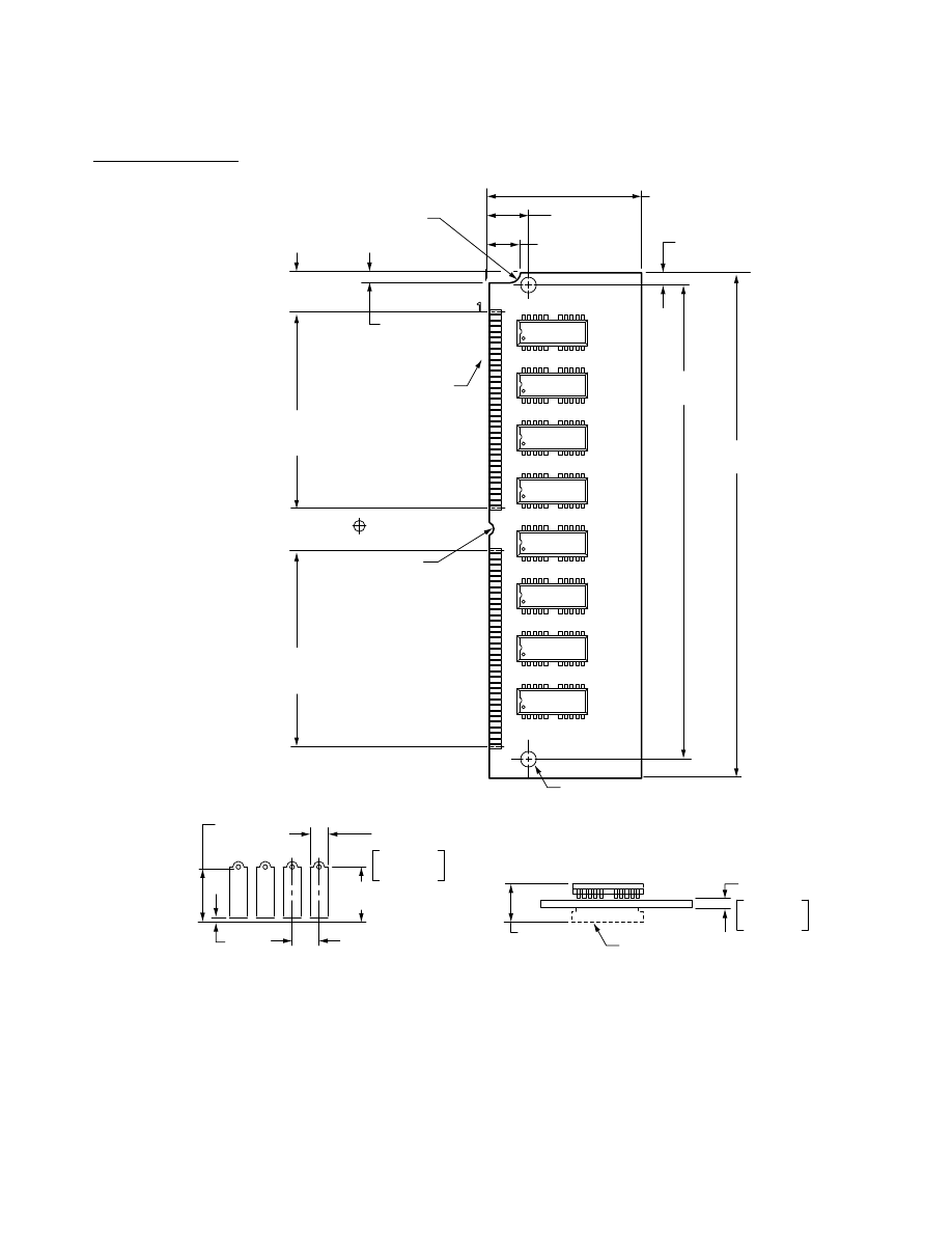
C H A P T E R 4
Expansion Features
50
RAM Expansion
Figure 4-1
RAM expansion SIMM
R 1.57
±
0.1
[.062
±
.004]
10.16
±
0.20
[.400
±
.008]
107.95
±
0.20
[4.25
±
.008]
101.19
±
0.20
[3.98
±
.008]
(6.35)
[.250]
6.35
±
0.20
[.250
±
.008]
25.4 [1.0]
Max
1.27 +0.10
- 0.08
+.004
- .003
.050
2X Ø3.18
±
0.1
[.125
±
.004]
9.4 [.37]
Max
2.54 [.100]
Min
1.27
±
0.10
[.050
±
.004]
0.25
[.010]
Max
Detail A
Rotated 90
°
CCW
35 X 1.27 [.050] =
44.45
±
0.20
[1.75
±
.008]
6.35
±
0.05
[.250
±
.002]
0.10 [.004] M A B
35 X 1.27 [.050] =
44.45
±
0.20
[1.75
±
.008]
2.03
±
0.20
[.080
±
.008]
See detail A
3.38
[.133]
2.03
[.080]
Min
R 1.57
±
0.12
[.062
±
.005]
0.90 +0.17
- 0.08
+.003
- .003
.035
Device on this
side optional.
Note: Dimensions are in millimeters with inches in brackets.

C H A P T E R 4
Expansion Features
The I/O Expansion Slot
51
The I/O Expansion Slot
4
The I/O expansion slot can accept either of two types of expansion cards: a 96-pin card
similar to the PDS card used in the Macintosh LC II or a 114-pin card similar to the PDS
card used in the Macintosh LC III.
IMPORTANT
Although often referred to as a processor-direct slot (PDS), the I/O
expansion slot in the Power Macintosh 5200 and 6200 computers is not
a true PDS because it is not connected directly to the main processor.
PDS cards designed to interact with the main processor—to provide,
for example, a RAM cache or an FPU—will not work in the I/O
expansion slot.
▲
The I/O Expansion Connector
4
The I/O expansion connector is mechanically the same as the PDS connector in the
Macintosh Quadra 630 and LC 630. It is essentially a 120-pin Euro-DIN connector with
six pins removed to make a notch. The notch divides the connector into two sections: a
96-pin section that accepts the 96-pin connector used on PDS cards for the
Macintosh LC II, and a separate 18-pin section for additional signals. For more
information see the section “Card Connectors” on page 57.
Connector Pin Assignments
4
Table 4-5 on page 52 gives the pin assignments for the I/O expansion connector. Pins 1
through 32 in all three rows (A, B, and C) correspond to the 96-pin section of the
connector. Pins 33 and 34 in all three rows are missing—those pins correspond to the
notch in the connector. Pins 35 through 40 in all three rows make up the 18-pin section of
the connector.
Except for one signal, 16MASTER (on pin B31 and described in Table 4-6 on page 54),
the pin assignments on the 96-pin section of the extended PDS are the same as those
on the PDS in the Macintosh LC II. On the Macintosh LC II, pin B31 is the Apple II
video clock input.
Note
Signal names starting with a slash (/) are active when their signal lines
are driven to a logical zero (0).
◆
IMPORTANT
Under no circumstances should you use the Analog GND pin (Pin 1,
Row B) for a digital ground on your expansion card. Doing so will cause
digital noise to be coupled into the audio system, resulting in degraded
sound quality.
▲

C H A P T E R 4
Expansion Features
52
The I/O Expansion Slot
Table 4-5
Pin assignments for the expansion connector
Pin
number
Row A
Row B
Row C
1
n. c.
Analog GND
/FPU.SEL
2
/SLOTIRQ
/R/W
/DS
3
/PDS.AS
+5V
/BERR
4
/PDS.DSACK1
+5V
/PDS.DSACK0
5
/HALT
SIZ1
SIZ0
6
FC2
GND
FC1
7
FC0
CLK16M
/RESET
8
/RMC
GND
/BG.SLOT
9
D31
D30
D29
10
D28
D27
D26
11
D25
D24
D23
12
D22
D21
D20
13
D19
D18
D17
14
D16
D15
D14
15
D13
D12
D11
16
D10
D9
D8
17
/BGACK
/BR_SLOT
A0
18
A1
A31
A27
19
A26
A25
A24
20
A23
A22
A21
21
A20
/IPL2
/IPL1
22
/IPL0
D3
D4
23
D2
D5
D6
24
D1
D0
D7
25
A4
A2
A3
26
A6
A12
A5
27
A11
A13
A7
28
A9
A8
A10
29
A16
A15
A14
30
A18
A17
A19
continued

C H A P T E R 4
Expansion Features
The I/O Expansion Slot
53
All the signals on the expansion connector are capable of driving at least one TTL load
(1.6 mA sink, 400
µ
A source). Most of the signals are connected to other MOS devices on
the main logic board; for those signals, the DC load on the bus signals is small. All the
data lines (D0–D31) are connected to the PrimeTime II custom IC so they have
CMOS-type loads.
Signal Descriptions
4
The I/O expansion slot is intended to be compatible with expansion cards designed
for computers that use the MC68030 microprocessor (the Macintosh LC III and
Macintosh LC 520 computers). Because the bus protocols on the 68040 I/O bus are
not the same as those of the MC68030, the signals on the I/O expansion slot are not
connected directly to the main processor . Instead, those signals are connected to the
PrimeTime II custom IC, which emulates the MC68030 control and data buses.
The upper 30 address lines (A31–2) are connected directly to the 68040 address bus. The
I/O bus adapter logic in the PrimeTime II IC provides the buffered data bus (IOD31–0)
and the two lowest address lines (A1–0).
31
n. c.
16MASTER
FC3
32
+12V
GND
–5V
33
(Pin not present)
(Pin not present)
(Pin not present)
34
(Pin not present)
(Pin not present)
(Pin not present)
35
A28
/BG.SLOT
C16M
36
A29
+5V
A30
37
/CIOUT
/CPU.AS
/STERM
38
/CBACK
n. c.
/CBREQ
39
n. c.
/CPU.DSACK0
n. c.
40
n. c.
GND
/CPU.DSACK1
Table 4-5
Pin assignments for the expansion connector (continued)
Pin
number
Row A
Row B
Row C

C H A P T E R 4
Expansion Features
54
The I/O Expansion Slot
Table 4-6 describes the signals on the I/O expansion connector.
Table 4-6
Descriptions of the signals on the I/O expansion connector
Signal name
Signal description
A0–A31
Address lines.
/BERR
Bus error; bidirectional signal indicating that an error occurred
during the current bus cycle; when /HALT is also asserted, /BERR
causes the bus cycle to be retried.
/BGACK
Bus grant acknowledge; input signal indicating that a device on the
card has become bus master.
/BG.SLOT
Bus grant to the slot; signal indicating that a device on the card can
become bus master following completion of the current processor
bus cycle (when /PDS.AS, /BGACK, and all the /DSACK signals
are inactive).
/BR.SLOT
Bus request from the slot; input signal indicating that a device on
the card is requesting to become bus master.
/CBACK
CPU burst acknowledge; used with /STERM during a burst
transfer to indicate that an individual element of a burst transfer
is ready.
/CBREQ
CPU burst request; used to initiate a quadruple longword burst
transfer; tied to a 4.7K pull-up resistor.
/CIOUT
Cache inhibit out signal from main processor, indicating that a
second-level cache is allowed to participate in the current bus
transaction; tied to a 300
Ω
pull-down resistor.
C16M
Same signal as CLK16M.
CLK16M
Independent clock running at 15.6672 MHz; provided for
compatibility with Macintosh LC and LC II PDS cards.
/CPU.AS
Address strobe; three-state signal indicating that an active bus
transaction is occurring.
/CPU.DSACK0,
/CPU.DSACK1
Data strobe acknowledge signals; asserted by the addressed bus
slave to end a bus transaction; also used to inform the master of the
size of the slave’s data port. These signals are electrically connected
to the corresponding /PDS.DSACK signals.
D0–D31
Data lines.
/DS
Data strobe. During a read operation, /DS is asserted when a
device on the card should place data on the data bus; during a write
operation, /DS is asserted when the main processor has put valid
data on the data bus.
FC0–FC2
Function code used to identify address space of current bus cycle;
tied to pull-up and pull-down resistors to indicate supervisor data
space accesses.
continued

C H A P T E R 4
Expansion Features
The I/O Expansion Slot
55
FC3
Additional function code bit, used to indicate that the software is
running in 32-bit address mode. (As in the Macintosh LC II, the
software always runs in 32-bit mode.)
/FPU.SEL
Select signal for an optional MC68881 or MC68882 FPU; tied to a
4.7K pull-up resistor; never asserted by the logic board in a
Macintosh LC 475 or Macintosh Quadra 605 computer.
/HALT
Used in conjunction with the /BERR signal to terminate a bus cycle
with a retry response; not used to stop processor execution.
/IPL0–IPL2
Interrupt priority-level lines.
/PDS.AS
Address strobe; synchronized to 16 MHz regardless of the actual
processor speed; asserted only when a valid slot address is being
generated by the bus master. When the card is the active bus
master, the card may drive either this signal or /CPU.AS, but
not both.
/PDS.DSACK0,
/PDS.DSACK1
Data strobe acknowledge signals; asserted by the addressed bus
slave to end a bus transaction; also used to inform the master of the
size of the slave’s data port. These signals are electrically connected
to the corresponding /CPU.DSACK signals.
/RESET
Bidirectional signal that initiates system reset.
/RMC
Three-state output signal that identifies the current bus cycle as part
of an indivisible bus cycle such as a read-modify-write operation.
/R/W
Read/write; three-state output signal that defines the direction of
the bus transfer with respect to the current bus master; logical one
(1) indicates a bus-master read, zero (0) indicates bus-master write.
16MASTER
Indicates the width of the data port when the card is alternate bus
master. A logical one (1) indicates a 16-bit port; logical zero (0)
indicates a 32-bit port. The signal is pulled high on the main
logic board.
SIZ0–SIZ1
Three-state output signals that work in conjunction with the
PrimeTime II IC’s dynamic bus sizing capabilities and indicate
the number of bytes remaining to be transferred during the
current bus cycle.
/SLOTIRQ
Interrupt request line from the card; reported to the system by way
of the SLOT.E request; when low, generates a level-2 interrupt if the
slot interrupt enable bit is set.
/STERM
Indicates termination of a synchronous transfer by a card using the
MC68030 synchronous cycle.
Table 4-6
Descriptions of the signals on the I/O expansion connector (continued)
Signal name
Signal description

C H A P T E R 4
Expansion Features
56
The I/O Expansion Slot
The /BG.SLOT signal appears on two pins; there is no separate CPU.BG signal. The
following signals on the expansion slot are permanently connected:
■
/PDS.DSACK0 is connected to /CPU.DSACK0
■
/PDS.DSACK1 is connected to /CPU.DSACK1
Unlike those signals, the /PDS.AS signal and the /CPU.AS signal are not connected
together. The /PDS.AS signal is used only for addresses in the slot $E address range; the
/CPU.AS signal is used for addresses in expansion slot and Super Slot spaces $6–$8,
$A–$D, and $F (the slot $9 address spaces are used for built-in video circuitry).
IMPORTANT
The I/O expansion slot does not support PowerPC 603 bus transfers.
The expansion slot does not support a processor operating at a clock
frequency other than 16 MHz.
▲
Bus Master on a Card
4
The I/O expansion slot will support a card with an MC68020 or MC68030 bus master.
The PrimeTime II custom IC controls bus arbitration between the card’s bus master and
the PowerPC 603 microprocessor so that either bus master will eventually obtain the bus.
The MC68020 or MC68030 will obtain the I/O data bus and the address bus. The
PowerPC 603 will obtain the processor data bus and the address bus. The Capella IC
synchronizes the bus arbitration between the PowerPC 603 and the 68040 address bus.
Because there is only one address bus, there can be only one bus master at a time.
Asynchronous transfers are the preferred method for data transfers to and from an I/O
expansion card. When an I/O expansion card contains an active bus master, the
PrimeTime II IC terminates successful data transfers using the DSACK signals. A slave
on the expansion card can also terminate a transfer using DSACK signals.
The PrimeTime II IC can never be a synchronous slave on the I/O bus, so PrimeTime II
cannot terminate data tansfers as a slave using /STERM. On the other hand, a bus slave
on an expansion card can terminate a 32-bit wide synchronous transfer using /STERM.
PrimeTime II supports /STERM terminations as a master on the I/O bus, and all
transfers from PrimeTime II to the expansion slot are based on the 16 MHz clock.
Incompatibility With Older Cards
4
While the I/O expansion slot will accept PDS cards designed for the Macintosh LC II
and LC III, some of those cards do not work. Cards that are incompatible with the
expansion slot include
■
cards designed to work as coprocessors with an MC68020 or an MC68030 or as
replacements for those microprocessors. Such cards include accelerators, 68882 FPU
cards, and cache cards. That type of card won’t work because the microprocessor is
different and because the slot signals are not connected directly to the microprocessor.

C H A P T E R 4
Expansion Features
The I/O Expansion Slot
57
■
cards with drivers that include incompatible code. Some drivers that do not follow
Apple Computer’s programming guidelines won’t work on machines that use the
PowerPC 603 microprocessor. For example, some of those drivers write directly to the
cache control register in an MC68030. Such code won’t work on a PowerPC 603.
■
cards with drivers that include code to check the
gestaltMachineType
value and
refuse to run on a newer CPU. The idea is to protect users by refusing to run on a
machine that the cards haven’t been tested on. Such cards have compatibility
problems with all new Macintosh models.
Designing an I/O Expansion Card
4
The I/O expansion card is approximately 3 inches wide by 5 inches long. It fits parallel
to the main logic board and reaches to an opening in the back of the case (normally filled
by a snap-out cover). The opening provides access to a 15-pin D-type connector on the
card for external I/O. For mechanical specifications of the I/O expansion card, see the
Appendix.
The appendix “Foldout Drawings” contains drawings showing the recommended
mechanical design guidelines for the expansion card. Foldout 1 shows the maximum
dimensions of the expansion card and the location of the expansion connector. Foldout 2
provides component height restrictions for the expansion card. Foldout 3 shows how the
card is installed on the main logic board.
Note
The I/O expansion card is the same size and shape as the
PDS card for the Macintosh LC III computer.
◆
Card Connectors
4
The custom 114-pin PDS connector on the computer’s main logic board accepts either a
96-pin or 120-pin standard Euro-DIN connector. You can order connectors meeting
Apple specifications from Amp Incorporated, Harrisburg, PA 17105 or from Augat
Incorporated, Interconnect Products Division, P. O. Box 779, Attleboro, MA 02703. Refer
to
Designing Cards and Drivers for the Macintosh Family
, third edition, for more information
about those connectors.
Power for the Card
4
The maximum current available at each supply voltage is shown in Table 4-7 on page 58.
The card must not dissipate more than 4 W total; for example, if the card uses the
maximum current at –5 V and +12 V, it must not use more than 300 mA from the
+5 V supply.
▲
W A R N I N G
Cards dissipating more than 4 watts may overheat and damage the
computer’s circuitry or cause it to become inoperable.
▲
C H A P T E R 4
Expansion Features
58
The I/O Expansion Slot
Card Address Space
4
The address space for the I/O expansion card appears in physical address spaces
$E000 0000–$EFFF FFFF and $FE00 0000–$FEFF FFFF. To match the conventions used
by the Slot Manager, software should address the card as if it were in slot space $E:
either the 16 MB slot space $FE00 0000–$FEFF FFFF or the Super Slot space
$E000 0000–$EFFF FFFF.
Card Select Signal
4
The I/O expansion card must generate its own select signal from the address and
function code signals on the connector. The card select signal must be disabled when
FC0, FC1, and FC2 are all active; that condition corresponds to a function code of 111
(CPU space). Figure 4-2 shows a typical logic circuit for generating the card select signal.
IMPORTANT
To ensure compatibility with future hardware and software, you should
minimize the chance of address conflicts by decoding all the address
bits. To ensure that the Slot Manager recognizes your card, the card’s
declaration ROM must reside at the upper address limit of the 16 MB
address space ($FE00 0000–$FEFF FFFF).
▲
Figure 4-2
Generating the card select signal
Table 4-7
Power available for the expansion card
Voltage
Current
+5
800 mA
–5
20 mA
+12
200 mA
A31
FC0
FC1
FC2
FC3
A23
A22
A21
A20
Card
select
32-bit mode
select
24-bit mode
select
Disable selection
on interrupt
acknowledge
cycles
C H A P T E R 4
Expansion Features
The DVA Connector
59
The DVA Connector
4
The optional video input card has a separate connector called the DVA (digital video
application) connector. The DVA connector provides access to the video input card’s
4:2:2 unscaled YUV video input data bus and associated control signals. By means of a
cable to the DVA connector, an I/O expansion card can gain access to the digital video
bus on the video input card and use it to transfer real-time video data to the computer.
Such an I/O expansion card can contain a hardware video compressor or other video
processor.
The DVA connector is a 34-pin flat ribbon connector located at the top edge of the video
input card. Figure 4-3 is a view of the main logic board showing the I/O expansion card
and the location of the DVA connector on the video input card.
Figure 4-3
Location of the DVA connector
Communications
module
I/O expansion card
Internal chassis
connector
DVA connector on
video input module
Video input module

C H A P T E R 4
Expansion Features
60
The DVA Connector
Figure 4-4 shows the orientation of the DVA connector on the video input module.
Figure 4-4
Orientation of the DVA connector
The DVA connector accepts YUV video and analog sound from the expansion card but
does not itself generate YUV video output or audio output signals.
IMPORTANT
The DVA connector on the video input card provides some of the
functionality of the DAV connectors found on the Power Macintosh 7100
and 8100 models and the Macintosh Quadra
AV
models, but it is not
compatible with either of those connectors. Refer to Macintosh DAV
Interface for NuBus Expansion Cards in Developer Note Number 8 for
more information.
▲
Pin Assignments
4
Table 4-8 shows the pin assignments on the DVA connector.
Table 4-8
Pin assignments on the DVA connector
Pin
number
Signal name
Pin
number
Signal name
1
UV(7)
2
UV(6)
3
UV(5)
4
UV(4)
5
UV(3)
6
UV(2)
7
UV(1)
8
UV(0)
9
Y(7)
10
Y(6)
11
Y(5)
12
Y(4)
continued
Pin 1
DVA connector

C H A P T E R 4
Expansion Features
The DVA Connector
61
Signal Descriptions
4
Table 4-9 gives descriptions of the signals on the DVA connector.
Using the YUV Bus
4
The video input module contains a digital video decoder and scaler (DESC), the Philips
SAA7196 IC. Logic on the video input card uses the CVBS port on the DESC and pulls
the DIR signal low, disabling the YUV bus. For an expansion card to use the YUV bus,
the software associated with the card must set the DIR signal high so that the DESC will
13
Y(3)
14
Y(2)
15
Y(1)
16
Y(0)
17
Ground
18
LLCB
19
Ground
20
CREFB
21
Ground
22
VS
23
Ground
24
HS
25
Ground
26
HREF
27
Ground
28
DIR
29
Reserved
30
Reserved
31
Ground
32
YUV_SND_LEFT
33
YUV_RET
34
YUV_SND_RIGHT
Table 4-9
Descriptions of the signals on the DVA connector
Signal name
Signal description
CREFB
Clock reference signal
DIR
YUV directional signal
HREF
Horizontal reference signal
HS
Horizontal sync signal
LLCB
Line-locked clock signal
UV(0–7)
Digital chrominance data bus
VS
Vertical sync signal
Y(0–7)
Digital luminance data bus
Table 4-8
Pin assignments on the DVA connector (continued)
Pin
number
Signal name
Pin
number
Signal name
C H A P T E R 4
Expansion Features
62
The DVA Connector
accept data on the YUV bus. To do that, the software can use the Cuda Dispatch
Manager to issue a IIC command to write to register $E of the DESC. For information
about using the registers in the DESC IC, please refer to the SAA7196 Philips Desktop
Video Handbook.
Video Data Format
4
Digital video data is transmitted as lines and fields. Each line consists of an even number
of samples on the Y and UV buses as shown in Figure 4-5. HREF is high during a video
line and low during the horizontal blanking interval. The falling edge of the VS signal
indicates the beginning of a video field. For more information about digital video data in
YUV format, see Macintosh DAV Interface for NuBus Expansion Cards in Developer Note
Number 8.
Figure 4-5
Video data timing
Y 0
LLCLK
vdcCREFB
HREF
Y 7–0
UV 7–0
Start of a video line
Y1
Y2
Y3
Y4
Y5
U 0
V0
U2
V2
U4
V4
Y and UV data valid on the rising edge of LLCLK
when HREF and CREFB are high
Yn-5
LLCLK
vdcCREFB
HREF
Y 7–0
UV 7–0
End of a video line
Yn-4
Yn-3
Yn-2
Yn-1
Yn
Un-5
Vn-5
Un-3
Vn-3
Un-1
Vn-1

C H A P T E R 4
Expansion Features
The Communications Slot
63
The Communications Slot
4
The main logic board has a separate slot for an optional communications card.
The communications slot supports 68030 protocol transfers with a 68030 bus master/
slave, SCC port A (modem port) for an Apple designed 2400 baud modem, and a special
serial port for an Apple designed 14,400 baud modem. The communications slot is
capable of supporting a 68030 bus master and contains one set of 68030 bus arbitration
control signals, but it does not support 68040 bus protocol transfers.
The communications slot connector is a 112-pin half-height microchannel connector.
A communications card mounts vertically in the connector and its I/O connector is
accessed through the communications port access hole on the right hand side of the back
panel. The size constraints of a communications card are 1.57 inches (40 mm) wide by
6 inches (152 mm) long.
A maximum of 2.5 watts of power are allocated to the communications slot. The
maximum possible current ratings for each power line are:
Table 4-10 shows the pin assignments of the communications slot.
Voltage
Current
+5 V
500 mA
+12 V
100 mA
Trickle +5 V
5 mA
–5 V
20 mA
Table 4-10
Pin assignments for the communucations slot connector
Pin
Function
Pin
Function
1
AUD.MtoH
2
AUD.HtoM
3
AUD.MHGND
4
AUD.MHGND
5
RW
6
/DS
7
/BERR
8
/DSACK1
9
/DSACK0
10
GND
11
IOSIZE(0)
12
C16M
13
IOSIZE(1)
14
GND
15
/RESET
16
/BG.SACTO
17
D31
18
D30
19
D29
20
D28
continued

C H A P T E R 4
Expansion Features
64
The Communications Slot
21
D27
22
D26
23
D25
24
D24
25
D23
26
D22
27
+5V
28
D21
29
D20
30
D19
31
D18
32
D17
33
D16
34
D15
35
D14
36
D13
37
D12
38
D11
39
D10
40
D9
41
D8
42
GND
43
D7
44
D6
45
D5
46
D4
47
D3
48
D2
49
D1
50
D0
51
/BGACK
52
/BR.SACTO
53
/IO.CS.TIMED
54
/IO.CS.DSACL
55
+5V
56
/SACTO.IRQ
57
A1
58
A0
59
A2
60
A3
61
A4
62
A5
63
A6
64
A7
65
A8
66
A9
67
A10
68
A11
69
A12
70
GND
71
A13
72
A14
73
A15
74
A16
75
A17
76
A18
77
A19
78
A20
79
A21
80
A22
81
A23
82
A24
continued
Table 4-10
Pin assignments for the communucations slot connector (continued)
Pin
Function
Pin
Function

C H A P T E R 4
Expansion Features
The Communications Slot
65
Note
Pin 100 must be pulled low for PowerPC-based computers.
◆
83
+5V
84
A25
85
A26
86
A27
87
A28
88
A29
89
A30
90
A31
91
/CPU.AS
92
GND
93
TRICKLE+5V
94
SYS.WAKEUP
95
BCLK
96
–5V
97
+12V
98
GND
99
EXT.AUD.RTN
100
Product Key
101
EXT.AUD.LEFT
102
Analog GND
103
MIC.SENSE
104
Int Mic
105
SCC.PORTA.ENB
106
IN.SENSE
107
TxDA
108
RxDA
109
RTSA
110
CTSA
111
DRTA
112
DCDA
Table 4-10
Pin assignments for the communucations slot connector (continued)
Pin
Function
Pin
Function


C H A P T E R 5
Software Features
5
Figure 5-0
Listing 5-0
Table 5-0

C H A P T E R 5
Software Features
68
ROM Software
The first part of this chapter describes the software in the ROM of the Power Macintosh
5200 and 6200 computers. The second part describes the system software that supports
the new features of these computers.
For a description of the system software for the internal IDE hard disk, see Chapter 6,
“Software for the IDE Hard Disk.”
ROM Software
5
The ROM is based on the ROM used in the current Power Macintosh models with the
necessary changes to support machine-specific hardware.
The following is a list of the most significant ROM changes:
■
Hardware Init now includes support for MMU programming and other PowerPC 603
microprocessor functions, addition of new diagnostics, and removal of the 68040
check/support code.
■
The nanokernal has been modified to support the PowerPC microprocessor.
■
The software no longer supports 1- or 2- bit video modes.
■
The software supports both 8 bit and 16 bit sound, depending on the configuration of
the hardware.
Machine Identification
5
The ROM includes new tables and code for identifying the two computers.
Applications can find out which computer they are running on by using the Gestalt
Manager routines; see
Inside Macintosh: Overview
. The
gestaltMachineType
value
returned by the Power Macintosh 5200 computer is 41 (hexadecimal $29). The Power
Macintosh 6200 computer returns a value of 42 (hexadecimal $2A).
System Software
5
The Power Macintosh 5200 and 6200 computersare shipped with a version of System 7.5
software preinstalled. System 7.5 Update 1.0 is included in the preinstalled system
software. The disk labeled “Install Me First” includes a
system enable
r file that contains
the resources the system needs to start up and initialize the computer.
As soon as the system software on disk takes over the startup process, it searches for all
system enablers that can start up the particular machine. Each system enabler contains a
resource that specifies which computers it is able to start up and the time and date of its
creation. If the system software finds more than one enabler for the particular computer,
it passes control to the one with the most recent time and date.

C H A P T E R 5
Software Features
System Software
69
In general, the system enabler included in each reference release of system software
is able to start up all previous computers. The enablers for computers introduced after
a reference release may be independent or may use resources from the previous
reference release
The system enabler includes modifications to the video digitizer allowing it to run in
native mode to improve video capture performance.


C H A P T E R 6
Software for the
IDE Hard Disk
6
Figure 6-0
Listing 6-0
Table 6-0
C H A P T E R 6
Software for the IDE Hard Disk
72
Introduction to IDE Software
This chapter describes the system software that controls an IDE hard disk drive installed
in a Macintosh computer. To use the information in this chapter, you should already be
familiar with writing programs for the Macintosh computer that call device drivers to
manipulate devices directly. You should also be familiar with the ATA IDE specification,
ANSI proposal X3T9.2/90-143, Revision 3.1.
Introduction to IDE Software
6
Support for IDE (integrated drive electronics) hard disk drives is incorporated in the
ROM software. System software for controlling IDE hard drives is included in a new IDE
hard disk drive device driver and the ATA Manager. The relationship of the IDE hard
disk drive device driver and the ATA Manager to the Macintosh system architecture is
shown in Figure 6-1.
Figure 6-1
Relationship of the ATA Manager to the Macintosh system architecture
CD-ROM
driver
SCSI
hard disk
driver
File Manager
Device Manager
ATA/IDE
hard disk
driver
CD-ROM
SCSI
hard disk
Other SCSI
devices
SCSI interface
Peripheral
devices
System
software
Application
SCSI Manager
ATA interface
ATA Manager
ATA/IDE
hard disk
Other SCSI
device
drivers

C H A P T E R 6
Software for the IDE Hard Disk
Introduction to IDE Software
73
At the system level, the IDE device driver and ATA Manager work in the same way that
the SCSI Manager and associated SCSI device drivers work. The IDE hard disk device
driver provides drive partition, data management, and error-handling services for the
Macintosh Operating System as well as support for determining device capacity and
controlling device-specific features. The ATA Manager provides an interface to the IDE
hard disk drive for the IDE device driver.
IDE hard disk drives appear on the desktop the same way SCSI hard disk drives
currently do. Except for applications that perform low-level services, such as formatting
and partitioning utilities, applications interact with the IDE hard disk drives in a device-
independent manner through the File Manager.
The IDE software for these computers supports only synchronous data transfers.
IDE Hard Disk Device Driver
6
The IDE hard disk device driver provides operating system-dependent services through
a set of driver routines required to interface with the Macintosh Operating System. In
addition, it provides additional control and status functions that are specific to this
implementation of the IDE hard disk device driver. The required driver routines, as
specified in
Inside Macintosh: Devices
, are
open
,
close
,
prime
,
control
, and
status
.
In addition to the required functions, the IDE hard disk device driver provides support
for device-specific features. IDE hard disk device driver control and status functions are
defined in “IDE Hard Disk Driver Reference” beginning on page 74.
At system startup time, if a RAM-based driver is not found on the IDE drive media, the
IDE device driver in the ROM is installed as one of the device drivers. Note that this is
different from the driver loading sequence for SCSI hard drive devices, which are RAM
based drivers that are always loaded from the device media.
The IDE hard disk device driver has a driver reference number of –54 (decimal) and a
driver name of
.ATDrvr.
Like all Macintosh device drivers, the IDE hard disk device
driver can be called by using either the
refNum
–54 or the driver name
.ATDrvr
.
The IDE hard disk device driver does not provide request queuing. All driver requests
are either completed immediately or are passed to the ATA Manager for further
processing. For further information about the control and status functions for the IDE
hard disk device driver, see “IDE Hard Disk Driver Reference.”
ATA Manager
6
The Macintosh ATA Manager schedules I/O requests from the IDE hard disk device
driver, the operating system, and applications. It is also responsible for managing the
hardware interface to the IDE controller electronics.
When making calls to the ATA Manager you have to pass and retrieve parameter
information through a parameter block. The size and content of the parameter block
depends on the function being called. However, all calls to the ATA Manager have a
common parameter block header structure. The structure of the
ataPBHdr
parameter

C H A P T E R 6
Software for the IDE Hard Disk
74
IDE Hard Disk Driver Reference
block is common to all ATA parameter block data types. Several additional ATA
parameter block data types have been defined for the various functions of the ATA
Manager. The additional parameter block data types, which are specific to the function
being called, are described in “ATA Manager Reference” beginning on page 83.
IDE Hard Disk Driver Reference
6
This section describes the Macintosh device driver functions provided by the IDE hard
disk device driver. The information in this section assumes that you are already familiar
with how to use device driver services on the Macintosh computer. If you are not
familiar with Macintosh device drivers, refer to the chapter “Device Manager” in
Inside
Macintosh: Devices
for additional information.
High-Level Device Manager Functions
6
The IDE hard disk driver supports the required set of high-level Device Manager
routines, as defined in the chapter “Device Manager” of
Inside Macintosh: Devices
. Those
routines are briefly defined here for convenience. Additional control functions supported
in the IDE hard disk driver are defined in “IDE Hard Disk Driver Control Functions”
beginning on page 77.
open
6
The
open
routine opens the IDE hard disk device driver during the startup sequence
after the driver code is retrieved from the ROM. The
open
routine returns a reference
number to the driver; that number is used in subsequent calls to the driver.
The following operations take place at startup time:
■
memory allocation and driver globals and internal variables initialization
■
power-on drive diagnostics
■
device detection and verification
■
device initialization
■
device information uploading
■
drive queue management and event posting
After startup, the driver responds with
noErr
to subsequent calls to the
open
routine
and does not repeat the operations performed at startup time.

C H A P T E R 6
Software for the IDE Hard Disk
IDE Hard Disk Driver Reference
75
RESULT CODES
close
6
The
close
routine deallocates the driver memory storage, removes the drive queue
entry point, and closes the IDE hard disk device driver.
RESULT CODES
prime
6
The
prime
routine performs either a
read
or
write
command as specified by the caller.
During this process the following operations take place:
■
byte to block translation
■
address translation
■
update of the
IOParameter
block
■
high-level error recovery and retry algorithm
■
ATA Manager parameter block management
Refer to “ATA Manager” on page 73 for more information about the parameter block
structure for the ATA Manager.
RESULT CODES
noErr
0
Successful completion, no error occurred
openErr
–23
Could not open the driver
DRVRCantAllocate
–1793
Global memory allocation error
ATABufFail
–1796
Device buffer test failed
noErr
0
Successful completion, no error occurred
noErr
0
Successful completion, no error occurred
ioErr
–36
I/O error
paramErr
–50
Invalid parameter specified
nsDrvErr
–56
No such drive installed

C H A P T E R 6
Software for the IDE Hard Disk
76
IDE Hard Disk Driver Reference
status
6
The
status
routine returns status information about the IDE hard disk device driver.
The type of information returned is specified in the
csCode
field and the information
itself is pointed to by the
csParamPtr
field.
The IDE hard disk device driver implements the same status functions supported by the
SCSI hard disk device driver. The status functions supported by the IDE hard disk driver
are shown in Table 6-1.
RESULT CODES
control
6
The
control
routine sends control information to the IDE hard disk device driver. The
type of control function is specified in
csCode
.
The IDE driver implements the same control functions supported by the SCSI hard disk
driver. The control functions are listed below and described in “IDE Hard Disk Driver
Control Functions” beginning on page 77.
Table 6-1
Status functions supported by the IDE hard disk driver
Value of
csCode
Definition
8
Return drive status information
43
Return driver Gestalt information
70
Power mode status information
noErr
0
Successful completion, no error occurred
statusErr
–18
Unimplemented status function; could not complete
requested operation
nsDrvErr
–56
No such drive installed
Value of
csCode
Definition
1
Kill I/O
5
Verify media
6
Format media
7
Eject media
21
Return drive icon
22
Return media icon
23
Return drive characteristics
65
Need-time code
70
Power-mode status management control

C H A P T E R 6
Software for the IDE Hard Disk
IDE Hard Disk Driver Reference
77
RESULT CODES
IDE Hard Disk Driver Control Functions
6
The IDE hard disk driver supports a standard set of control functions for IDE hard disk
drive devices. The functions are used for control, status, and power management.
killIO
6
The
killIO
function is a standard function defined in Inside Macintosh: Devices .
IMPORTANT
This function is not supported by the IDE hard disk driver. A call to
KillIO
returns a
controlErr
status.
▲
verify
6
The
verify
function requests a read verification of the data on the IDE hard drive
media. This function performs no operation.
An arrow preceding a parameter indicates whether the parameter is an input parameter,
an output parameter, or both: .
Parameter block
RESULT CODES
noErr
0
Successful completion, no error occurred
controlErr
–17
Unimplemented control function; could not complete
requested operation
nsDrvErr
–56
No such drive installed
Arrow
Meaning
→
Input
←
Output
↔
Both
→
csCode
A value of 5.
→
ioVRefNum
The logical drive number.
→
csParam[]
None defined.
←
ioResult
See result codes.
noErr
0
Successful completion, no error occurred.
nsDrvErr
–56
The specified logical drive number does not exist.

C H A P T E R 6
Software for the IDE Hard Disk
78
IDE Hard Disk Driver Reference
format
6
The
format
function initializes the hard drive for use by the operating system. Because
IDE hard drives are low-level formatted at the factory, this function does not perform
any operation. The driver always returns
noErr
if the logical drive number is valid.
Parameter block
RESULT CODES
ejectMedia
6
The
ejectMedia
function prepares and initiates an eject operation from the specified
drive. This function applies only to drives with removable media.
Note
The
ejectMedia
function is not supported by the IDE hard disk driver;
this function returns a
noErr
if the logical drive number is valid.
◆
Parameter block
RESULT CODES
return drive icon
6
The
return drive icon
function returns a pointer to the device icon and the device
name string. The drive icon is the same as the media icon for IDE hard disk drives. The
drive icon for IDE hard disk devices is shown in Figure 6-2.
Figure 6-2
IDE hard disk drive icon
→
csCode
A value of 6.
→
ioVRefNum
The logical drive number.
→
csParam[]
None defined.
←
ioResult
See result codes.
noErr
0
Successful completion, no error occurred.
nsDrvErr
–56
The specified logical drive number does not exist.
→
csCode
A value of 7.
→
ioVRefNum
The logical drive number.
→
csParam[]
None defined.
←
ioResult
See result codes.
noErr
0
Successful completion, no error occurred.
nsDrvErr
–56
The specified logical drive number does not exist.

C H A P T E R 6
Software for the IDE Hard Disk
IDE Hard Disk Driver Reference
79
Parameter block
RESULT CODES
return media icon
6
The
return media icon
function returns a pointer to the media icon and the name
string. The media icon is the same as the drive icon for IDE hard disk drives, as shown
in Figure 6-2.
Parameter block
RESULT CODES
return drive characteristics
6
The
return drive characteristics
function returns information about the
characteristics of the specified drive as defined in Inside Macintosh, Volume V.
Parameter block
RESULT CODES
→
csCode
A value of 21.
→
ioVRefNum
The logical drive number.
→
csParam[]
None defined.
←
csParam[0–1]
Address of drive icon and name string
(information is in
ICN#
format).
←
ioResult
See result codes.
noErr
0
Successful completion, no error occurred.
nsDrvErr
–56
The specified logical drive number does not exist.
→
csCode
A value of 22.
→
ioVRefNum
The logical drive number.
→
csParam[]
None defined.
←
csParam[0–1]
Address of drive icon and name string
(information is in
ICN#
format).
←
ioResult
See result codes.
noErr
0
Successful completion, no error occurred.
nsDrvErr
–56
The specified logical drive number does not exist.
→
csCode
A value of 23.
→
ioVRefNum
The logical drive number.
→
csParam[]
None defined.
←
csParam[0–1]
Drive information.
$0601 = primary, fixed, SCSI, internal.
$0201 = primary, removable, SCSI, internal.
←
ioResult
See result codes.
noErr
0
Successful completion, no error occurred.
nsDrvErr
–56
The specified logical drive number does not exist.

C H A P T E R 6
Software for the IDE Hard Disk
80
IDE Hard Disk Driver Reference
needTime code
6
The
needTime code
function provides time for the driver to perform periodic opera-
tions such as checking for media insertion or ejection events related to removable
cartridge drives. For additional information about how this function is used, see the
description of the driver flag
dNeedTime
in the chapter “Device Manager” of
Inside
Macintosh: Devices. This function performs no operation on the IDE hard disk drive in
these computers.
Parameter block
RESULT CODES
power management
6
The
power management
function can be used to reduce drive power consumption and
decrease system noise levels by putting the hard drive into a standby state.
Note
The
power management
control function is most useful on PowerBook
computers, where it can be used to reduce drive power consumption
and thereby extend useful battery life.
◆
The
power management
function provides three modes of operation for IDE hard disk
drives: idle, standby, and sleep.
In the idle state, the nonessential electronics on the IDE hard drive are disabled. For
example, the read and write channels are disabled during the idle state. The spindle
motor remains enabled during the idle state, so the drive still responds immediately to
any commands requesting media access.
In the standby state, the head is parked and the spindle motor is disabled. The drive
interface remains active and is still capable of responding to commands. However, it can
take several seconds to respond to media access commands, because the drive’s spindle
motor must return to full speed before media access can take place.
In the sleep state, the drive interface and spindle motor are disabled. To return the drive
to full operation after the sleep state has been enabled, the user must restart or reset
the computer.
→
csCode
A value of 65.
→
csParam[]
None defined.
←
ioResult
See result codes.
noErr
0
Successful completion, no error occurred.
nsDrvErr
–56
The specified logical drive number does not exist.

C H A P T E R 6
Software for the IDE Hard Disk
IDE Hard Disk Driver Reference
81
Parameter block
RESULT CODES
drive status info
6
The IDE hard disk device driver provides a drive status function for retrieving status
information from the drive. The
drive status info
function returns the same type
of information that disk drivers are required to return for the
status
function,
as described in the chapter “Device Manager” in Inside Macintosh: Devices.
Parameter block
RESULT CODES
return driver gestalt
6
The
return driver gestalt
function provides the application information about
the IDE hard disk driver and the attached device. Several calls are supported under this
function. A Gestalt selector is used to specify a particular call.
→
csCode
A value of 70.
→
ioVRefNum
The logical drive number.
→
csParam[0]
The most significant byte contains one of the
following codes:
0 = enable the active mode
1 = enable the standby mode
2 = enable the idle mode
3 = enable the sleep mode
←
ioResult
See result codes.
noErr
0
Successful completion, no error occurred.
controlErr
–17
The power management information couldn’t be
returned due to a manager error.
nsDrvErr
–56
The specified logical drive number does not exist.
→
csCode
A value of 8.
→
ioVRefNum
The logical drive number.
→
csParam[]
The
csParam
field contains status information
about the internal IDE disk drive.
←
ioResult
See result codes.
noErr
0
Successful completion, no error occurred.
nsDrvErr
–56
The specified logical drive number does not exist.

C H A P T E R 6
Software for the IDE Hard Disk
82
IDE Hard Disk Driver Reference
The
DriverGestaltParam
data type defines the IDE Gestalt parameter block:
typedef struct DriverGestaltParam
{
ataPBHdr
/* See definition on page 73 */
short
ioVRefNum;
/* refNum of device */
short
csCode;
/* Driver gestalt code */
OSType
driverGestaltSelector;
/* Gestalt selector */
driverGestaltInfo
driverGestaltResponse;
/* Returned result */
} DriverGestaltParam;
The fields
driverGestaltSelector
and
driverGestaltResponse
are 32-bit fields.
Parameter block
→
csCode
A value of 43.
→
ioVRefNum
The logical drive number.
→
driverGestaltSelector
Gestalt function selector. This is a 32-bit ASCII
field containing one of the following selectors:
sync
Indicate synchronous or
asynchronous driver.
devt
Specify type of device the driver
is controlling.
intf
Specify the device interface.
boot
Specify PRAM value to designate
this driver or device.
vers
Specify the version number of the
driver.
←
driverGestaltResponse
Returned result based on the driver gestalt
selector. The possible four-character return
values are:
TRUE
If the
sync
driver selector is
specified, this Boolean value
indicates that the driver is
synchronous; a value of
FALSE
indicates asynchronous.
disk
If the
devt
driver selector is
specified, this value indicates a hard
disk driver.
ide
If the
intf
driver selector is
specified, this value indicates the
interface is IDE.
0
If the
boot
driver selector is
specified, this value indicates that
this is the boot driver or boot device.
nnnn
If the
vers
selector is specified, the
current version number of the driver
is returned.
←
ioResult
See result codes.

C H A P T E R 6
Software for the IDE Hard Disk
ATA Manager Reference
83
RESULT CODES
power-mode status
6
The
power-mode status
function returns the current power mode state of the internal
hard disk.
Parameter block
RESULT CODES
ATA Manager Reference
6
This section defines the data structures and functions that are specific to the ATA
Manager. The section “The ATA Parameter Block” shows the data structure of the ATA
parameter block. The “Functions” section describes the functions for managing and
performing data transfers through the ATA Manager.
The ATA Parameter Block
6
This section defines the fields that are common to all ATA Manager functions that use the
ATA parameter block. The fields used for specific functions are defined in the description
of the functions to which they apply. You use the ATA parameter block for all calls to the
ATA Manager. The
ataPBHdr
data type defines the ATA parameter block.
The parameter block includes a field,
MgrFCode
, in which you specify the function
selector for the particular functionto be executed; you must specify a value for this field.
Each ATA function may use different fields of the ATA parameter block for parameters
specific to that function.
noErr
0
Successful completion, no error occurred.
nsDrvErr
–56
The specified logical drive number does not exist.
statusErr
–18
Unknown selector was specified.
→
csCode
A value of 70.
→
ioVRefNum
The logical drive number.
→
csParam[]
None defined.
←
csParam[]
The most significant byte of this field contains
one of the following values:
1 = drive is in standby mode
2 = drive is in idle mode
3 = drive is in sleep mode
←
ioResult
See result codes.
noErr
0
Successful completion, no error occurred.
nsDrvErr
–56
The specified logical drive number does not exist.
statusErr
–18
The power management information couldn’t be
returned due to a manager error.

C H A P T E R 6
Software for the IDE Hard Disk
84
ATA Manager Reference
An arrow preceding the comment indicates whether the parameter is an input parameter,
an output parameter, or both.
The ATA parameter block header structure is defined as follows:
typedef
unsigned char
uchar;
typedef
unsigned short
ushort;
typedef
unsigned long
ulong;
typedef
struct
ataPBHdr
/* ATA Manager parameter block
header structure */
{
Ptr
ataLink;
/* Reserved */
short
ataQType;
/* Type byte */
uchar
ataPBVers;
/*
→
Parameter block
version number */
uchar
hdrReserved;
/* Reserved */
Ptr
hdrReserved2;
/* Reserved */
ProcPtr
ataCompletion; /* Completion routine */
short
ataResult;
/*
←
Returned result */
uchar
MgrFCode;
/*
→
Manager function code */
uchar
ataIOSpeed;
/*
→
I/O timing class */
ushort
ataFlags;
/*
→
Control options */
short
hdrReserved3;
/* Reserved */
long
deviceID;
/*
→
Device ID */
ulong
TimeOut;
/*
→
Transaction timeout
value */
Ptr
ataPtr1;
/* Client storage Ptr 1 */
Ptr
ataPtr2;
/* Client storage Ptr 2 */
ushort
ataState;
/* Reserved, init to 0 */
short
hdrReserved4;
/* Reserved */
long
hdrReserved5;
/* Reserved */
} ataPBHdr;
Field descriptions
ataLink
This field is reserved for use by the ATA Manager. It is used
internally for queuing I/O requests. It must be initialized to 0
before calling the ATA Manager.
ataQType
This field is the queue type byte. It should be initialized to 0 before
calling the ATA Manager.
ataPBVers
This field contains the parameter block version number. A value of
1 is the only value currently supported. Any other value results in a
paramErr
.
Arrow
Meaning
→
Input
←
Output
↔
Both

C H A P T E R 6
Software for the IDE Hard Disk
ATA Manager Reference
85
hdrReserved
This field is reserved for future use. To ensure future compatibility,
all reserved fields should be set to 0.
hdrReserved2
This field is reserved for future use. To ensure future compatibility,
all reserved fields should be set to 0.
ataCompletion
This field contains the completion routine pointer to be called upon
completion of the request. When this field is set to 0, it indicates a
synchronous I/O request; a non-zero value indicates an
asynchronous I/O request. The routine this field points to is called
when the request has finished without error, or when the request
has terminated due to an error. This field is valid for any manager
request. The completion routine is called as follows:
pascal void (*RoutinePtr) (ataIOPB *)
The completion routine is called with the associated manager
parameter block in the stack.
ataResult
Completion status. This field is returned by the ATA Manager after
the request is completed. Refer to Table 6-6 on page 102 for a list of
the possible error codes returned in this field.
MgrFCode
This field is the function selector for the ATA Manager. The
functions are defined in Table 6-4 on page 88. An invalid code in
this field results in an
ATAFuncNotSupported
error.
ataIOSpeed
This field specifies the I/O cycle timing requirement of the specified
IDE drive. This field should contain word 51 of the identify drive
data. Currently values 0 through 3 are supported, as defined in
the ATA IDE specification. See the ATA IDE specification for the
definitions of the timing values. If a timing value higher than one
supported is specified, the manager operates in the fastest timing
mode supported by the manager. Until the timing value is deter-
mined by examining the identify drive data returned by the
ATA_Identify
function, the client should request operations
using the slowest mode (mode 0).
ataFlags
This 16-bit field contains control settings that indicate special
handling of the requested function. The control bits are defined in
Table 6-3 on page 86.
hdrReserved3
This field is reserved for future use. To ensure future compatibility,
all reserved fields should be set to 0.
deviceID
A short word that uniquely identifies an IDE device. This field
consists of the following structure:
typedef struct
/* Device ID structure */
{
ushort Reserved;
/* The upper word is reserved */
ushort deviceNum;
/* Consists of device ID and
bus ID */
} deviceIdentification;
Bit 15 of the
deviceNum
field indicates master (=0) /slave (=1)
selection. Bits 14 through 0 contain the bus ID (for example, 0x0 =
master unit of bus 0, 0x80 = slave unit of bus 0). The present
implementation allows only one device in the master configuration.
This value is always 0.

C H A P T E R 6
Software for the IDE Hard Disk
86
ATA Manager Reference
TimeOut
This field specifies the transaction timeout value in milliseconds. A
value of zero disables the transaction timeout detection.
ataPtr1
This pointer field is available for application use. It is not modified
by the ATA Manager.
ataPtr2
This pointer field is available for application use. It is not modified
by the ATA Manager.
ataState
This field is used by the ATA Manager to keep track of the current
bus state. This field must contain zero when calling the manager.
Bus states are defined in Table 6-2.
hdrReserved4
This field is reserved for future use. To ensure future compatibility,
all reserved fields should be set to 0.
hdrReserved5
This field is reserved for future use. To ensure future compatibility,
all reserved fields should be set to 0.
Table 6-2 lists the states of the IDE drive bus.
Table 6-3 describes the functions of the control bits in the
ataFlags
field.
Table 6-2
IDE drive bus states
Code
Name
Description
$00
Initial
Parameter block processing started
$01
Started
Command delivery state
$0F
Data
Data delivery state
$1F
Status
Status delivery state
$3F
Complete
Bus transaction complete state
$FF
Idle
Waiting to return state
Table 6-3
Control bits in the
ataFlags
field
Name
Bit
Definition
—
0–2
Reserved.
RegUpdate
3
When set to 1 this bit indicates that a set of device
registers should be reported back upon completion
of the request. This bit is valid for the
ATA_ExecI/O
function only. Refer to the description on page 89
for details. The following device registers are
reported back:
Sector count register
Sector number register
Cylinder register(s)
SDH register
continued

C H A P T E R 6
Software for the IDE Hard Disk
ATA Manager Reference
87
—
4–7
Reserved.
SGType
8, 9
This 2-bit field specifies the type of scatter gather list
passed in. This field is only valid for read/write
operations.
The following types are defined:
00 = Scatter gather disabled
01 = Scatter gather type I enabled
10 = Reserved
11 = Reserved
When set to 0, this field indicates that the
ioBuffer
field contains the host buffer address for this transfer,
and the
ioReqCount
field contains the byte transfer
count.
When set to 1, this field indicates that the
ioBuffer
and the
ioReqCount
fields of the parameter block for
this request point to a host scatter gather list and the
number of scatter gather entries in the list, respectively.
The format of the scatter gather list is a series of the
following structure definition:
typedef struct
/* SG entry structure */
{
uchar* ioBuffer;
/*
→
Data buffer pointer */
ulong ioReqCount;
/*
→
Byte count */
} IOBlock;
QLockOnError
10
When set to 0, this bit indicates that an error during the
transaction should not freeze the I/O queue for the
device. When an error occurs on an I/O request with
this bit set to 0, the next queued request is processed
following this request. When an error occurs on an
I/O request with this bit set to 1, the user must issue an
ATA_QRelease
command to continue. A status code
of hexadecimal 717 is returned for subsequent
asynchronous I/O requests until the
I/O Queue Release
command is issued.
Immediate
11
When this bit is set to 1, it indicates that the request
must be executed as soon as possible and the status of
the request must be returned. It forces the request to the
head of the I/O queue for immediate execution. When
this bit is set to 0, the request is queued in the order
received and is executed according to that order.
continued
Table 6-3
Control bits in the
ataFlags
field (continued)
Name
Bit
Definition

C H A P T E R 6
Software for the IDE Hard Disk
88
ATA Manager Reference
Functions
6
This section describes the ATA Manager functions that are used to manage and perform
data transfers. Each function is requested through a parameter block specific to that
service. A request for an IDE function is specified by a function code within the
parameter block. The entry point for all the functions is the same.
ATA Manager function names and codes are shown in Table 6-4.
ATAioDirection
12,
13
This bit field specifies the direction of data transfer. Bit
values are binary and defined as follows:
00 = No data transfer
10 = Data direction in (read)
01 = Data direction out (write)
11 = Reserved
—
14
Reserved.
ByteSwap
15
When set to 1, this bit indicates that every byte of data
prior to transmission on write operations and upon
reception on read operations is to be swapped. When
this bit is set to 0, it forces bytes to go out in the
LSB-MSB format compatible with IBM clones.
Typically, this bit should be set to 0. Setting this bit has
performance implications because the byte swap is
performed by the software. Use this bit with caution.
Table 6-4
ATA Manager functions
Function name
Code
Description
ATA_ExecIO
$01
Execute ATA I/O
ATA_MgrInquiry
$90
ATA Manager inquiry
ATA_MgrInit
$91
Initialize ATA Manager
ATA_BusInquiry
$03
Bus inquiry
ATA_QRelease
$04
I/O queue release
ATA_NOP
$00
No operation
ATA_Abort
$10
Terminate command
ATA_RegAccess
$12
ATA device register access
ATA_Identify
$13
Get the drive identification data
ATA_ResetBus
$11
Reset IDE bus
continued
Table 6-3
Control bits in the
ataFlags
field (continued)
Name
Bit
Definition

C H A P T E R 6
Software for the IDE Hard Disk
ATA Manager Reference
89
ATA_ExecIO
6
You can use the
ATA_ExecIO
function to perform all data I/O transfers to or from an
IDE device. Your application must provide all of the parameters needed to complete the
transaction prior to calling the ATA Manager. Upon return, the parameter block contains
the result of the request.
A prior call to the
ATA_MgrInit
function to initialize the ATA Manager must be
performed before issuing the
ATA_ExecIO
function. See page 93 for information about
the
ATA_MgrInit
function.
The manager function code for the
ATA_ExecIO
function is $01.
The parameter block associated with the
ATA_ExecIO
function is defined below:
typedef
struct
/* ATA_ExecIO structure */
{
ataPBHdr
/* See definition on page 84 */
char
ataStatusReg;
/*
←
Last device status register
image */
char
ataErrorReg;
/*
←
Last device error register
image (valid if bit 0 of Status
field is set) */
short
ataReserved;
/* Reserved */
ulong
BlindTxSize;
/*
→
Data transfer size */
IOBlock
IOBlk;
/*
→
Data transfer
descriptor block */
ulong
ataActualTxCnt;
/*
←
Actual number of bytes
transferred */
ulong
ataReserved2;
/* Reserved */
devicePB RegBlock;
/*
→
Device register images */
uchar*
packetCDBPtr;
/* ATAPI packet command block
pointer */
ushort
ataReserved3[6];
/* Reserved */
} ATA_ExecIO;
ATA_MgrShutDown
$92
Shutdown ATA Manager
ATA_DrvrRegister
$85
Register the driver reference number
ATA_DrvrDeregister
$87
Deregister the driver reference number
ATA_FindRefNum
$86
Look up the driver reference number
Table 6-4
ATA Manager functions (continued)
Function name
Code
Description

C H A P T E R 6
Software for the IDE Hard Disk
90
ATA Manager Reference
Field descriptions
ataStatusReg
This field contains the last device status register image. See the ATA
IDE specification for status register bit definitions.
ataErrorReg
This field contains the last device error register image. This field is
valid only if the error bit (bit 0) of the
Status
register is set. See the
ATA IDE specification for error register bit definitions.
ataReserved
Reserved. All reserved fields are set to 0 for future compatibility.
BlindTxSize
This field specifies the maximum number of bytes that can be
transferred for each interrupt or detection of a data request. Bytes
are transferred in blind mode (no byte level handshake). Once an
interrupt or a data request condition is detected, the ATA Manager
transfers up to the number of bytes specified in the field from or to
the selected device. The typical number is 512 bytes.
IOBlk
This field contains either the host buffer address and the requested
transfer length, or the pointer to a scatter gather list and the number
of scatter gather entries. If the
SGType
bits of the
ataFlags
field
are set, the
IOBlk
field contains the scatter gather information. The
IOBlk
field is defined as follows:
typedef
struct
{
uchar*
ioBuffer;
/*
↔
Data buffer ptr */
ulong
ioReqCount; /*
↔
Transfer length */
} IOBlk;
ioBuffer
This field contains the host buffer address for the
number of bytes specified in the
ioReqCount
field.
Upon returning, the
ioBuffer
field is updated to
reflect data transfers. When the
SGType
bits of the
ataFlags
field are set, the
ioBuffer
field points
to a scatter gather list. The scatter gather list
consists of a series of
IOBlk
entries.
ioReqCount
This field contains the number of bytes to transfer
either from or to the buffer specified in
ioBuffer
.
Upon returning, the
ioReqCount
field is updated
to reflect data transfers (0 if successful; otherwise,
the number of bytes that remained to be transferred
prior to the error condition). When the
SGType
bits
of the
ataFlags
field are set, the
ioReqCount
field contains the number of scatter gather entries
in the list pointed to by the
ioBuffer
field.
ataActualTxCnt
This field contains the total number of bytes transferred for this
request. This field is currently not supported.
ataReserved2
This field is reserved. To ensure future compatibility, all reserved
fields should be set to 0.
RegBlock
This field contains the IDE device register image structure. Values
contained in this structure are written out to the device during the
command delivery state. The caller must provide the image prior to

C H A P T E R 6
Software for the IDE Hard Disk
ATA Manager Reference
91
calling the ATA Manager. The IDE device register image structure is
defined as follows:
typedef
struct
/* Device register images */
{
uchar
Features;
/*
→
Features register
image */
uchar
Count;
/*
↔
Sector count */
uchar
Sector;
/*
↔
Sector start/finish */
uchar
Reserved;
/* Reserved */
ushort
Cylinder;
/*
↔
Cylinder 68000 format */
uchar
SDH;
/*
↔
SDH register image */
uchar
Command;
/*
→
Command register image */
} Device_PB;
packetCDBPtr
This field contains the packet pointer for ATAPI. The current
version of the ATA Manager doesn’t support the ATAPI protocol.
For ATA commands, the
packetCDBPtr
field should contain 0 in
order to ensure compatibility in the future.
ataReserved3[6]
These fields are reserved. To ensure future compatibility, all
reserved fields should be set to 0.
RESULT CODES
noErr
0
Successful completion, no error occurred
nsDrvErr
–56
Specified logical drive number does not exist
AT_AbortErr
–1780
Command aborted bit set in error register
AT_RecalErr
–1781
Track 0 not found bit set in error register
AT_WrFltErr
–1782
Write fault bit set in status register
AT_ASeekErr
–1783
Seek complete bit not set upon completion
AT_UncDataErr
–1784
Uncorrected data bit set in error register
AT_CorDataErr
–1785
Data corrected bit set in status register
AT_BadBlkErr
–1786
Bad block bit set in error register
AT_DMarkErr
–1787
Data mark not found bit set in error register
AT_IDNFErr
–1788
ID not found bit set in error register
ATABusyErr
–1790
Selected device busy (BUSY bit set)
ATAMgrNotInitialized
–1802
ATA Manager not initialized
ATAPBInvalid
–1803
Invalid device base address detected (= 0)
ATATransTimeOut
–1806
Timeout: transaction timeout detected
ATAReqInProg
–1807
I/O channel in use—cannot proceed
ATAUnknownState
–1808
Device in unknown state
ATAQLocked
–1809
I/O queue locked—cannot proceed

C H A P T E R 6
Software for the IDE Hard Disk
92
ATA Manager Reference
ATA_MgrInquiry
6
The
ATA_MgrInquiry
function gets information, such as the version number, about the
ATA Manager. This function may be called prior to the manager initialization, however
the system configuration information may be invalid.
The manager function code for the
ATA_MgrInquiry
function is $90.
The parameter block associated with this function is defined below:
typedef
struct
/* IDE inquiry structure */
{
ataPBHdr
/* See definition on page 84 */
NumVersion
MgrVersion
ushort
MGRPBVers;
/*
←
Manager PB version number
supported */
ushort
Reserved1;
/* Reserved */
ushort
ataBusCnt;
/*
←
Number of ATA buses in
system */
ushort
ataDevCnt;
/*
←
Number of ATA devices
detected */
unchar
ataMaxMode;
/*
←
Maximum I/O speed mode */
ushort
Reserved2;
/* Reserved */
ushort
IOClkResolution; /*
←
I/O clock in nsec */
ushort
Reserved[17];
/* Reserved */
} ATA_MgrInquiry;
Field descriptions
ataPBHdr
See the definitionof the
ataPBHdr
parameter block on page 84.
MgrVersion
Upon return, this field contains the version number of the
ATA Manager.
MGRPBVers
This field contains the number corresponding to the latest version
of the parameter block supported. A client may use any parameter
block definition up to this version.
Reserved
Reserved. All reserved fields are set to 0 for future compatibility.
ataBusCnt
Upon return, this field contains the total number of ATA buses in
the system. This field contains a zero if the ATA Manager has not
been initialized.
ataDevCnt
Upon return, this field contains the total number of ATA devices
detected on all ATA buses. The current architecture allows only one
device per bus. This field will contain a zero if the ATA Manager
has not been initialized.
ataMaxMode
This field specifies the maximum I/O speed mode that the ATA
Manager supports. Refer to the ATA IDE specification for
information on mode timing.

C H A P T E R 6
Software for the IDE Hard Disk
ATA Manager Reference
93
IOClkResolution
This field contains the I/O clock resolution in nanoseconds. The
current implementation doesn’t support this field (returns 0).
Reserved[17]
This field is reserved. To ensure future compatibility, all reserved
fields should be set to 0.
RESULT CODES
ATA_MgrInit
6
You must call the
ATA_MgrInit
function prior to issuing
ATA_ExecIO
,
ATA_BusInquiry
,
ATA_QRelease
, or
ATA_Abort
commands. Otherwise, an
IDEMgrNotInitialized
error is returned. This function initializes internal variables and IDE hard disk drive
hardware. Consecutive initializationfunctions from either the same or another
application are ignored and
NoErr
is returned.
The manager function code for the
ATA_MgrInit
function is $91.
The parameter block associated with this function is defined below:
typedef
struct
/* IDE Init structure */
{
ataPBHdr
/* See definition on page 84 */
ushort
Reserved[24]
/* Reserved */
} ATA_MgrInit;
Field descriptions
ataPBHdr
See the definition of the
ataPBHdr
parameter block on page 84.
Reserved[24]
This field is reserved. To ensure future compatibility, all reserved
fields should be set to 0.
RESULT CODES
ATA_BusInquiry
6
The
ATA_BusInquiry
function gets information about a specific ATA bus. This function
is provided for possible future expansion of the Macintosh ATA architecture.
The manager function code for the
ataBusInquiry
function is $03.
noErr
0
Successful completion, no error occurred
noErr
0
Successful completion, no error occurred
ATAInitFail
–1795
ATA Manager initialization failure

C H A P T E R 6
Software for the IDE Hard Disk
94
ATA Manager Reference
The parameter block associated with this function is defined below:
typedef struct
/* IDE bus inquiry structure */
{
ataPBHdr
/* See definition on page 84 */
ushort
ataEngineCount;
/*
←
TBD; zero for now */
ushort
ataReserved;
/* Reserved */
ulong
ataDataTypes;
/*
←
TBD; zero for now */
ushort
ataIOpbSize;
/*
←
Size of ATA I/O PB */
ushort
ataMaxIOpbSize;
/*
←
TBD; zero for now */
ulong
ataFeatureFlags;
/*
←
TBD */
uchar
ataVersionNum;
/*
←
HBA Version number */
uchar
ataHBAInquiry;
/*
←
TBD; zero for now */
ushort
ataReserved2;
/* Reserved */
ulong
ataHBAPrivPtr;
/*
←
Ptr to HBA private data */
ulong
ataHBAPrivSize;
/*
←
Size of HBA private data */
ulong
ataAsyncFlags;
/*
←
Capability for callback */
ulong
ataReserved3[4];
/* Reserved */
ulong
ataReserved4;
/* Reserved */
char
ataReserved5[16];
/* TBD */
char
ataHBAVendor[16];
/*
←
HBA Vendor ID */
char
ataContrlFamily[16];/*
←
Family of ATA controller */
char
ataContrlType[16];
/*
←
Controller model number */
char
ataXPTversion[4];
/*
←
Version number of XPT */
char
ataReserved6[4];
/* Reserved */
char
ataHBAversion[4];
/*
←
Version number of HBA */
uchar
ataHBAslotType;
/*
←
Type of slot */
uchar
ataHBAslotNum;
/*
←
Slot number of the HBA */
ushort
ataReserved7;
/* Reserved */
ulong
ataReserved8;
/* Reserved */
} ATA_BusInquiry;
Field descriptions
ataPBHdr
See the definition of the
ataPBHdr
structure on page 84.
ataEngineCount
This field is currently set to 0.
ataReserved
Reserved. All reserved fields are set to 0.
ataDataTypes
Not supported by current ATA architecture. Returns a bit map of
data types supported by this HBA. The data types are numbered
from 0 to 30; 0 through 15 are reserved for Apple definition and 16
through 30 are available for vendor use. Returns 0.
ataIOpbSize
This field contains the size of the I/O parameter block supported.
ataMaxIOpbSize
This field specifies the maximum I/O size for the HBA. This field is
currently not supported and returns 0.

C H A P T E R 6
Software for the IDE Hard Disk
ATA Manager Reference
95
ataFeatureFlags
This field specifies supported features. This field is not supported; it
returns a value of 0.
ataVersionNum
The version number of the HBA is returned. The current version
returns a value of 1.
ataHBAInquiry
Reserved.
ataHBAPrivPtr
This field contains a pointer to the HBA’s private data area. This
field is not supported; it returns a value of 0.
ataHBAPrivSize
This field contains the byte size of the HBA’s private data area. This
field is not supported; it returns a value of 0.
ataAsyncFlags
These flags indicate which types of asynchronous events the HBA is
capable of generating. This field is not supported; it returns a value
of 0.
ataHBAVendor
This field contains the vendor ID of the HBA. This is an ASCII text
field. It is not supported.
ataContrlFamily
Reserved.
ataContrlType
This field identifies the specific type of ATA controller. This field is
not supported; it returns a value of 0.
ataXPTversion
Reserved.
ataHBAversion
This field specifies the version of the HBA. This field is not
supported; it returns a value of 0.
ataHBAslotType
This field specifies the type of slot. This field is not supported; it
returns a value of 0.
ataHBAslotNum
This field specifies the slot number of the HBA. This field is not
supported; it returns a value of 0.
RESULT CODES
ATA_QRelease
6
The
ATA_QRelease
function releases the frozen I/O queue of the selected device.
When the ATA Manager detects an I/O error and the
QLockOnError
bit of the
parameter block is set for the request, the ATA Manager freezes the queue for the
selected device. No pending or new requests are processed or receive status until the
queue is released through the
ATA_QRelease
function. Only those requests with
the
Immediate
bit set in the
ATAFlags
field of the
ataPBHdr
parameter block are
processed. Consequently, for the ATA I/O queue release command to be processed, it
must be issued with the
Immediate
bit set in the parameter block. An ATA I/O queue
release command issued while the queue isn’t frozen returns the
noErr
status.
The manager function code for the
ATA_QRelease
function is $04.
There are no additional function-specific variations on
ataPBHdr
for this function.
noErr
0
Successful completion, no error occurred
ATAMgrNotInitialized
–1802
ATA Manager not initialized

C H A P T E R 6
Software for the IDE Hard Disk
96
ATA Manager Reference
RESULT CODES
ATA_NOP
6
The
ATA_NOP
function performs no operation across the interface and does not
change the state of either the manager or the device. It returns
noErr
if the drive
number is valid.
The manager function code for the
ATA_NOP
function is $00.
There are no additional function-specific variations on
ataPBHdr
for this function.
RESULT CODES
ATA_Abort
6
The
ATA_Abort
function terminates a specified queued I/O request. This function
applies to asynchronous I/O requests only. The
ATA_Abort
function searches through
the I/O queue associated with the selected device and aborts the matching I/O request.
The current implementation does not abort if the found request is in progress. If the
specified I/O request is not found or has started processing, an
ATAUnableToAbort
status is returned. If aborted, the
ATAReqAborted
status is returned.
It is up to the application that called the
ATA_Abort
function to clean up the aborted
request. Clean up includes parameter block deallocation and O/S reporting.
The manager function code for the
ATA_Abort
function is $10.
The parameter block associated with this function is defined as follows:
typedef
struct
/* IDE abort structure */
{
ataPBHdr
/* See definition on page 84 */
ATA_PB*
AbortPB
/* Address of the parameter block of
the function to be aborted */
ushort
Reserved
/* Reserved */
} ATA_Abort;
Field descriptions
ataPBHdr
See the definition of the
ataPBHdr
parameter block on page 83.
AbortPB
This field contains the address of the I/O parameter block to
be aborted.
Reserved
This field is reserved. To ensure future compatibility, all reserved
fields should be set to 0.
noErr
0
Successful completion, no error occurred
nsDrvErr
–56
Specified drive does not exist
ATAMgrNotInitialized
–1802
ATA Manager not initialized
noErr
0
Successful completion, no error occurred
nsDrvErr
–56
Specified drive does not exist

C H A P T E R 6
Software for the IDE Hard Disk
ATA Manager Reference
97
RESULT CODES
ATA_RegAccess
6
The
ATA_RegAccess
function enables access to a particular device register of a selected
device. This function is used for diagnostic and error recovery processes.
The manager function code for the
ATA_RegAccess
function is $12.
The parameter block associated with this function is defined below:
typedef
struct
/* Register access structure */
{
ataPBHdr
/* See definition on page 84 */
ushort
RegSelect
/*
→
Device register selector */
uchar
RegValue;
/*
↔
Register value
to read or to be written */
uchar
Reserved;
/*
↔
Used for data register
(LSB) only */
uchar
Reserved[22]
/* Reserved */
} ATA_RegAccess;
Field descriptions
ataPBHdr
See the definition of the
ataPBHdr
parameter block on page 84.
RegSelect
This field specifies which of the device registers to access. The
selectors for the registers supported by the
ATA_RegAccess
function are listed in Table 6-5.
RegValue
This field represents the value to be written (
IDEioDirection =
01b
) or the value read from the selected register
(
ATAioDirection
=
10
binary). For
DataReg
, it is assumed this
field is a 16-bit field; for other registers, an 8-bit field.
Reserved[22]
This field is reserved. To ensure future compatibility, all reserved
fields should be set to 0.
noErr
0
Successful completion, no error occurred
nsDrvErr
–56
Specified drive does not exist
ATAMgrNotInitialized
–1802
ATA Manager not initialized
ATAReqAborted
–1810
The request was aborted
ATAUnableToAbort
–1811
Request to abort couldn’t be honored
Table 6-5
IDE register selectors
Selector name
Selector
Register description
DataReg
0
Data register (16-bit access only)
ErrorReg
1
Error register (R) or features register (W)
SecCntReg
2
Sector count register
SecNumReg
3
Sector number register
continued

C H A P T E R 6
Software for the IDE Hard Disk
98
ATA Manager Reference
RESULT CODES
ATA_Identify
6
The
ATA_Identify
function returns the device identification data from the selected
device. The identification data contains information necessary to perform I/O to the
device. Refer to the ATA IDE Specification for the format and the information
description provided by the data.
The manager function code for the
ATA_Identify
function is $13.
The parameter block associated with this function is defined below:
typedef
struct
{
ataPBHdr
ushort
Reserved1[4];
/* Reserved */
uchar
*DataBuf;
/*
↔
Buffer for the data */
ushort
Reserved2[18];
/* Reserved */
} ATA_Identify;
Field descriptions
ataPBHdr
See the definition of the
ataPBHdr
parameter block on page 84.
DataBuf
A pointer to the data buffer for the device identify data. The length
of the buffer must be at least 512 bytes.
Reserved1[4],
Reserved2[18]
These fields are reserved. To ensure future compatibility, all
reserved fields should be set to 0.
RESULT CODES
CylLoReg
4
Cylinder low register
CylHiReg
5
Cylinder high register
SDHReg
6
SDH register
StatusReg
CmdReg
7
Status register (R) or command register (W)
AltStatus
DevCntr
14
Alternate status (R) or device control (W)
AddrReg
15
Digital input register
noErr
0
Successful completion, no error occurred
nsDrvErr
–56
Specified drive does not exist
noErr
0
Successful completion, no error occurred
nsDrvErr
–56
Specified drive does not exist
Table 6-5
IDE register selectors (continued)
Selector name
Selector
Register description

C H A P T E R 6
Software for the IDE Hard Disk
ATA Manager Reference
99
ATA_ResetBus
6
The
ATA_ResetBus
function performs a soft reset operation to the selected IDE bus.
The IDE interface doesn’t provide a way to reset individual units on the bus.
Consequently, all devices on the bus will be reset.
IMPORTANT
This function should be used with caution since it may terminate any
active requests to devices on the bus.
▲
The manager function code for the
ATA_ResetBus
function is $11.
The parameter block associated with this function is defined below:
typedef
struct
/* IDE reset structure */
{
ataPBHdr
/* See definition on page 84 */
char
Status;
/*
←
Last ATA status register image */
char
Reserved;
/* Reserved */
ushort
Reserved[23];
/* Reserved */
} ATA_ResetBus;
Field descriptions
ataPBHdr
See the definition of the
ataPBHdr
parameter block on page 84.
Status
This field contains the last device status register image following
the bus reset. See the ATA IDE specification for definitions of the
status register bits.
Reserved[23]
This field is reserved. To ensure future compatibility, all reserved
fields should be set to 0.
RESULT CODES
ATA_MgrShutDown
6
The
ATA_MgrShutDown
function shuts down the ATA Manager. It is the complement to
the
ATA_MgrInit
function. This function deallocates all of the global space currently in
use by the ATA Manager. After calling
ATA_MgrShutDown
, the ATA Manager must be
reinitialized before any IDE I/O requests can take place.
The
ATA_MgrShutDown
function always returns a status of
noErr
.
The manager function code for the
ATA_MgrShutDown
function is $92.
There are no additional function-specific variations on
ataPBHdr
for this function.
noErr
0
Successful completion, no error occurred
nsDrvErr
–56
Specified drive does not exist

C H A P T E R 6
Software for the IDE Hard Disk
100
ATA Manager Reference
IMPORTANT
This function should be used with caution if
multiple client applications are present.
▲
RESULT CODES
ATA_DrvrRegister
6
The
ATA_DrvrRegister
function registers the driver reference number passed in for
the selected drive. The function doesn’t check for the existence of another driver.
The manager function code for the
ATA_DrvrRegister
function is $85.
The parameter block associated with this function is defined below:
typedef
struct
/* Driver register structure */
{
ataPBHdr
/* See definition on page 84 */
short
drvrRefNum;
/*
→
Driver reference number */
ushort
FlagReserved;
/* Reserved */
ushort
deviceNextID;
/* Not used */
short
Reserved[21];
/* Reserved */
} ATA_DrvrRegister;
Field descriptions
ataPBHdr
See the
ataPBHdr
parameter block definition on page 84.
drvrRefNum
This field specifies the driver reference number to be registered.
This value must be less than 0 to be valid.
FlagReserved
Reserved.
deviceNextID
Not used by this function.
Reserved[21]
This field is reserved. To ensure future compatibility, all reserved
fields should be set to 0.
RESULT CODES
ATA_DrvrDeregister
6
The
ATA_DrvrDeRegister
function deregisters the driver reference number passed in
for the selected drive. After successful completion of this function, the driver reference
number for the drive is set to 0, which indicates that there is no driver in control of
this device.
The manager function code for the
ATA_DrvrDeRegister
function is $87.
noErr
0
Successful completion, no error occurred
noErr
0
Successful completion, no error occurred
nsDrvErr
–56
Specified drive does not exist

C H A P T E R 6
Software for the IDE Hard Disk
ATA Manager Reference
101
There are no additional function-specific variations on
ataPBHdr
for this function.
RESULT CODES
ATA_FindRefNum
6
The
ATA_FindRefNum
function allows an application to determine whether a driver has
been installed for a given device. You pass in a device ID and the function returns the
current driver reference number registered for the given device. A value of 0 indicates
that no driver has been registered. The
deviceNextID
field contains a device ID of the
next device in the list. The end of the list is indicated with a value of
0xFF
.
To create a list of all drivers for the attached devices, pass in
0xFF
for
deviceID
. This
causes
deviceNextID
to be filled with the first device in the list. Each successive driver
can be found by moving the value returned in
deviceNextID
into
deviceID
until the
function returns
0xFF
in
deviceNextID
, which indicates the end of the list.
The manager function code for the
ATA_FindRefNum
function is $86.
The parameter block associated with this function is defined as follows:
typedef
struct
{
ataPBHdr
short
drvrRefNum;
/*
←
Contains the driver refNum */
ushort
FlagReserved;
/* Reserved */
ushort
deviceNextID;
/*
←
Contains the next drive ID */
short
Reserved[21];
/* Reserved */
} ATA_FindRefNum;
Field descriptions
ataPBHdr
See the
ataPBHdr
parameter block definition on page 83.
drvrRefNum
Upon return, this field contains the reference number for the device
specified in the
deviceID
field of the
ataPBHdr
data.
FlagReserved
This field is reserved. To ensure future compatibility, all reserved
fields should be set to 0.
deviceNextID
Upon return, this field contains the
deviceID
of the next device on
the list.
Reserved[21]
This field is reserved. To ensure future compatibility, all reserved
fields should be set to 0.
RESULT CODES
noErr
0
Successful completion, no error occurred
nsDrvErr
–56
Specified drive does not exist
noErr
0
Successful completion, no error occurred
nsDrvErr
–56
Specified drive does not exist

C H A P T E R 6
Software for the IDE Hard Disk
102
Error Code Summary
Error Code Summary
6
A summary of the IDE hard disk drive error codes is provided in Table 6-6.
Table 6-6
IDE hard disk drive error codes
Error
code
Name
Description
0
noErr
No error detected on the request operation.
–17
controlErr
Unimplemented control function. Requested
control operation could not complete.
–18
statusErr
Unimplemented status function. Requested
status operation could not complete.
–23
openErr
Unimplemented open function. Open operation
could not complete.
–36
ioErr
An I/O error detected while processing
the request.
–50
paramErr
Error in parameter block.
–56
nsDrvErr
No such drive. No device attached to the
specified port.
–65
offLinErr
No disk in drive (removable media).
–1780
AT_AbortErr
Command aborted by drive. Unsupported
command.
–1781
AT_RecalErr
Recalibrate failure detected by device.
–1782
AT_WrFltErr
Write fault detected by device.
–1783
AT_SeekErr
Seek error detected by device.
–1784
AT_UncDataErr
Unable to correct data (possibly bad data).
–1785
AT_CorDataErr
Data was corrected (good data)—notification.
–1786
AT_BadBlkErr
Bad block detected by device.
–1787
AT_DMarkErr
Data mark not found reported by device.
–1788
AT_IDNFErr
Sector ID not found; error reported by device.
–1789
AT_DRQErr
Timeout waiting for DRQ active.
–1790
AT_BusyErr
Timeout waiting for BSY inactive.
–1791
AT_NRdyErr
Drive ready condition not detected.
–1793
DRVRCantAllocate
Driver memory allocation error during
driver open.
–1794
NoATAMgr
No ATA Manager installed in the system
(
MgrInquiry
failure).
–1795
ATAInitFail
ATA Manager initialization failed.

C H A P T E R 6
Software for the IDE Hard Disk
Error Code Summary
103
–1796
ATABufFail
Power-on device test failed. Device failure
detected. Interface communication error.
–1802
ATAMgrNotInitialized
ATA Manager has not been initialized. The
request function cannot be performed until
initialized.
–1803
ATAPBInvalid
Invalid IDE port address detected (ATA Manager
initialization problem).
–1804
ATAFuncNotSupported
An unknown manager function code specified.
–1805
ATABusy
Selected device is busy. The device isn’t ready to
go to next phase yet.
–1806
ATATransTimeOut
Timeout condition detected. The operation hasn’t
completed within the user specified time limit.
–1807
ATAReqInProg
Device busy; the device on the port is busy
processing another command.
–1808
ATAUnknownState
The device status register reflects an
unknown state.
–1809
ATAQLocked
The I/O queue for the port is locked due to a
previous I/O error (and must be unlocked prior
to continuing).
–1810
ATAReqAborted
The I/O queue entry was aborted due to an abort
command.
–1811
ATAUnableToAbort
The I/O queue entry could not be aborted. Too
late to abort or the entry not found.
Table 6-6
IDE hard disk drive error codes (continued)
Error
code
Name
Description


A P P E N D I X
105
Foldout Drawings
A
This appendix contains foldout pages with the mechanical drawings for the I/O expan-
sion card. Foldout 1 is a design guide showing the dimensions of the expansion card.
Foldout 2 shows the maximum component height permitted on the card. Foldout 3
is an assembly guide for the expansion card.
Figure A-0
Listing A-0
Table A-0
Expansion card design guide
062-0487-B
1 of 3
FOLDOUT 1
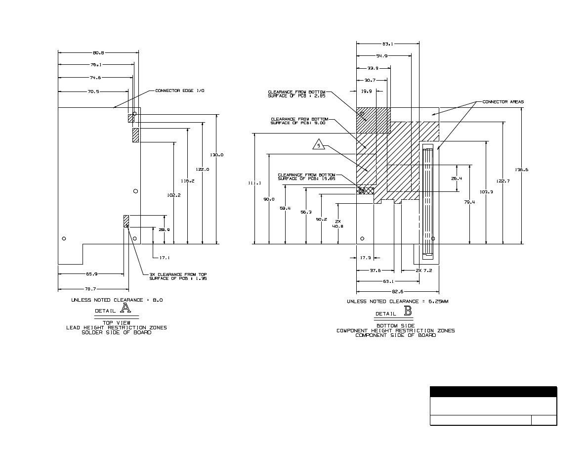
Expansion card component height restrictions
062-0487-B
2 of 3
FOLDOUT 2
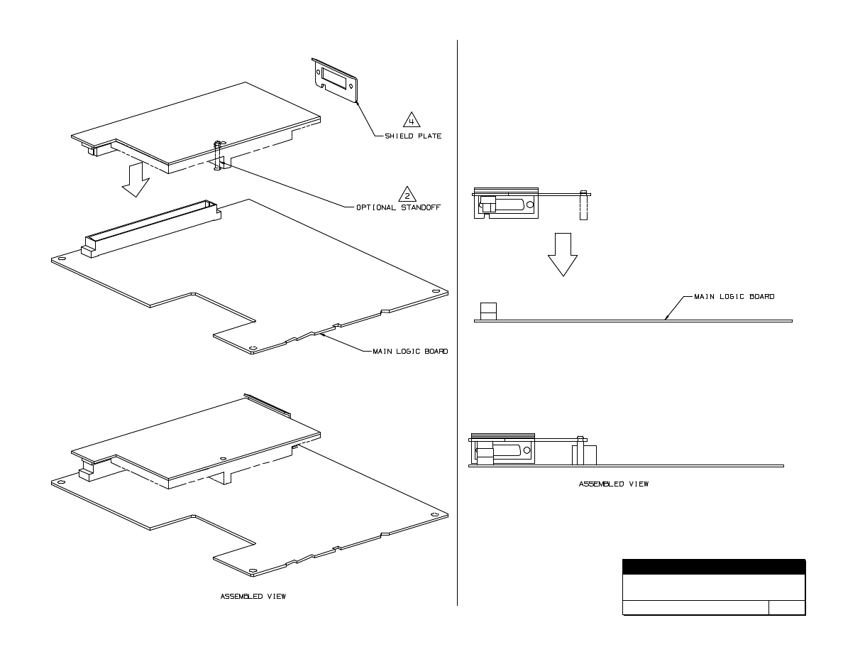
Expansion card assembly guide
062-0487-B
3 of 3
FOLDOUT 3

113
Index
A
abbreviations xii–xiv
ADB (Apple Desktop Bus) ports 25
ADB connector 25
ADB controller 18
address map 21–22
Apple IIe card incompatibility 20
Apple SuperDrive 26
ATA_Abort
function 96
ATA_BusInquiry
function 93
ATA_DrvrDeregister
function 100
ATA_DrvrRegister
function 100
ATA_ExecIO
function 89
ATA_FindRefNum
function 101
ATA_Identify
function 98
ATA IDE specification 72
ATA interface 27
ATA Manager 72, 83–103
making calls to 83
parameter block 74
purpose of 73
ATA Manager functions
ATA_Abort
96
ATA_BusInquiry
93
ATA_DrvrDeregister
100
ATA_DrvrRegister
100
ATA_ExecIO
89
ATA_FindRefNum
101
ATA_Identify
98
ATA_MgrInit
93
ATA_MgrInquiry
92
ATA_MgrShutDown
99
ATA_NOP
96
ATA_QRelease
95
ATA_RegAccess
97
ATA_ResetBus
99
ATA_MgrInit
function 93
ATA_MgrInquiry
function 92
ATA_MgrShutDown
function 99
ATA_NOP
function 96
ATA parameter block header 84
ataPBHdr
structure 84–88
ATA_QRelease
function 95
ATA_RegAccess
function 97
ATA_ResetBus
function 99
.ATDrvr
driver name 73
B
back view 5
block diagram 15
bus arbitration 19
bus masters 19
byte steering 17
C
Capella IC 16
clock speed 14
close
routine 75
color lookup table (CLUT) 19
communications modules 9
communications slot 63
compatibility
IDE hard disk 12
PDS cards 11, 56
connectors
ADB 25
DVA 59–61
floppy disk 26
hard disk 29
I/O, on I/O expansion card 57
for I/O expansion card 57
I/O expansion slot 51
SCSI 31
serial I/O 24
sound input jack 18, 32
sound output jacks 18, 32
video input 8
control
routine 76
Cuda IC 18
custom ICs 16
Capella IC 16
Cuda 18
DFAC II 18
F108 17
PrimeTime II 17, 53
Valkyrie 19

I N D E X
114
D
DAV connector in other models 60
DFAC II custom IC 18
digital video scaler IC 62
display memory 19, 21
display RAM 20
addresses for 21
driverGestalt
parameter block 82
drive status info
function 81
DVA connector 59–62
compared with DAV connector 60
pin assignments 60
signal descriptions 61
video data format 62
on video input module 59
dynamic bus sizing 17
E
ejectMedia
function 78
Ethernet card
10BaseT 9
10Base2 9
expansion slot.
See
I/O expansion slot
F
F108 custom IC 17
features summary 2
floppy disk connector 26
floppy disk drive 26
format
function 78
front view 4
G
gestaltMachineType
value 68
Gestalt Manager 68
GPi (general purpose input) signal 25
H
hard disk 12, 27
dimensions 27
hard disk connector 29
pin assignments on 29
signals on 30
I, J
IDE disk interface 27
IDE hard disk 12, 27
connector 27
pin assignments on 29
dimensions 27
signals 30
IDE hard disk device driver 73, 74–83
close
routine 75
control functions 77–83
control
routine 76
Device Manager routines 74–77
driverGestalt
parameter block 82
driver name 73
driver reference number 73
drive status info
function 81
ejectMedia
function 78
format
function 78
killIO
function 77
making calls to 73
needTime code
function 80
open
routine 74
power management
function 80
prime
routine 75
return drive characteristics
function 79
return drive icon
function 78
return driver gestalt
function 81
return media icon
function 79
status
routine 76
verify
function 77
IDE hard disk drives, compared with SCSI drives 73
IDE software
ATA Manager 72, 73
device driver 72
hard disk device driver 73
IDE specification 72
I/O bus 14
I/O expansion card 57–58
address space 21, 58
bus master on 56
card-select signal 58
connector for 57
design guidelines 57
I/O connector on 57
power 57
I/O expansion slot 51–58
compatibility with PDS cards 51, 56
connector 51

I N D E X
115
I/O expansion slot
(continued)
MC68030 compatibility 53
not a PDS 51
pin assignments 51
signal descriptions 53, 54
signal loading 53
support for bus master 56
use of Analog GND pin 51
K
keyboard
Power key 7
reset and NMI functions 34
L
L2 cache.
See
second-level cache
logic board, access to 6
M
machine identification 68
Macintosh Quadra 605 computer 3
MC68HC05 microcontroller 18
MC68LC040 microprocessor
clock speed 14
features of 14
memory control IC.
See
F108 custom IC
microphone 32
power for 32
mirror output 9, 35
modem card 9
modem port 24, 25
N
needTime code
function 80
O
open
routine 74
optional modules
communications 9
TV tuner 7
video display mirror out 9
video input 8
P, Q
parameter RAM 18
PDS cards, compatibility with 11, 56
PDS slot.
See
I/O expansion slot
power, for I/O expansion card 57
Power key
on keyboard 7
on remote control 7
power management
function 80
power-mode status
function 83
prime
routine 75
PrimeTime II custom IC 17
I/O bus adaptor in 53
R
RAM
address space 21
configurations 44
expansion 44–50
RAM SIMM 44–50
access time 47
address lines 48
address multiplexing 48
devices 47–48
JEDEC specification for 49
mechanical specifications 49
signal assignments 45–47
sizes 47
remote control 8
return drive characteristics
function 79
return drive icon
function 78
return driver gestalt
function 81
return media icon
function 79
ROM software 68
S
safe shut down 7
screen buffers 19
SCSI bus termination 32
SCSI connector 31
second-level cache (L2) 2
serial I/O ports 24
modem power 25
sound
buffers 18, 34
filters 33
input routing 33

I N D E X
116
sound (continued)
modes of operation 34
playthrough feature 34
routing of inputs 33
sample rates 33
sample size 33
sound circuits in the DFAC II IC 18
sound input jack 18, 32
sound output jacks 18, 32
standard abbreviations xii–xiv
status
routine 76
summary of features 2
system bus 14
T, U
terminator, for SCSI bus 32
32-bit addressing 21
TV picture sizes 7
TV tuner module 7
picture sizes 7
TV channels 8
with video input module 8
V, W, X
Valkyrie IC 19
verify
function 77
video data format 62
video display mirror output 9, 35
video input module 8
DVA connector on 59
input connectors 8
input from TV tuner module 8
monitors supported 9
window size 9
video monitors
colors displayed 36
timing parameters 38–41
types and sizes 38
video RAM. See display memory
Y, Z
YUV digital video 59, 62
for clearer picture 5, 8
data format of 62


T H E A P P L E P U B L I S H I N G S Y S T E M
This Apple manual was written, edited,
and composed on a desktop publishing
system using Apple Macintosh computers
and FrameMaker software. Proof pages
and final pages were created on an Apple
LaserWriter Pro 630 printer. Line art
was created using Adobe
Illustrator.
PostScript
, the page-description
language for the LaserWriter, was
developed by Adobe Systems
Incorporated.
Text type is Palatino
and display type
is Helvetica
. Bullets are ITC Zapf
Dingbats
. Some elements, such as
program listings, are set in Apple Courier.
WRITER
Rolly Reed
COPY EDITOR
Wendy Krafft
ILLUSTRATORS
Shawn Morningstar and Sandee Karr
Document Outline
- Power Macintosh 5200/75 and Power Macintosh 6200/75 Computers
Wyszukiwarka
Podobne podstrony:
Pro Staff 3 PPC 3H id 392593 Nieznany
5200
04 The Reformationid 5200 ppt
Zespół Szkół Rolniczych w Kijanac1 ppc
PPC ziemia 2b
5200
6200
6200
nowe plany ICP IPCH PPC PL mgr Nieznany
6200
6200
zag ppc, Notatki Bezpieczeństwo wewnętrzne, Kardas WSEI
5200
RF 5200 FALCON TRYBY PRAC, łączność
PPC test
6200
więcej podobnych podstron