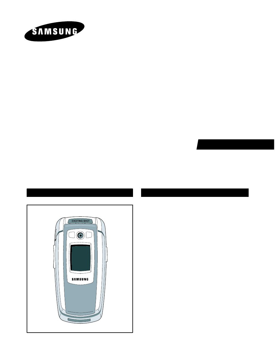
SGH-E710
SERVICE
Manual
GSM TELEPHONE
CONTENTS
1.
Specification
2.
Flow Chart of Troubleshooting
3.
Exploded Views and Parts List
4.
Electrical Parts List
5.
Block Diagrams
6.
PCB Diagrams
GSM TELEPHONE
SAMSUNG Proprietary-Contents may change without notice
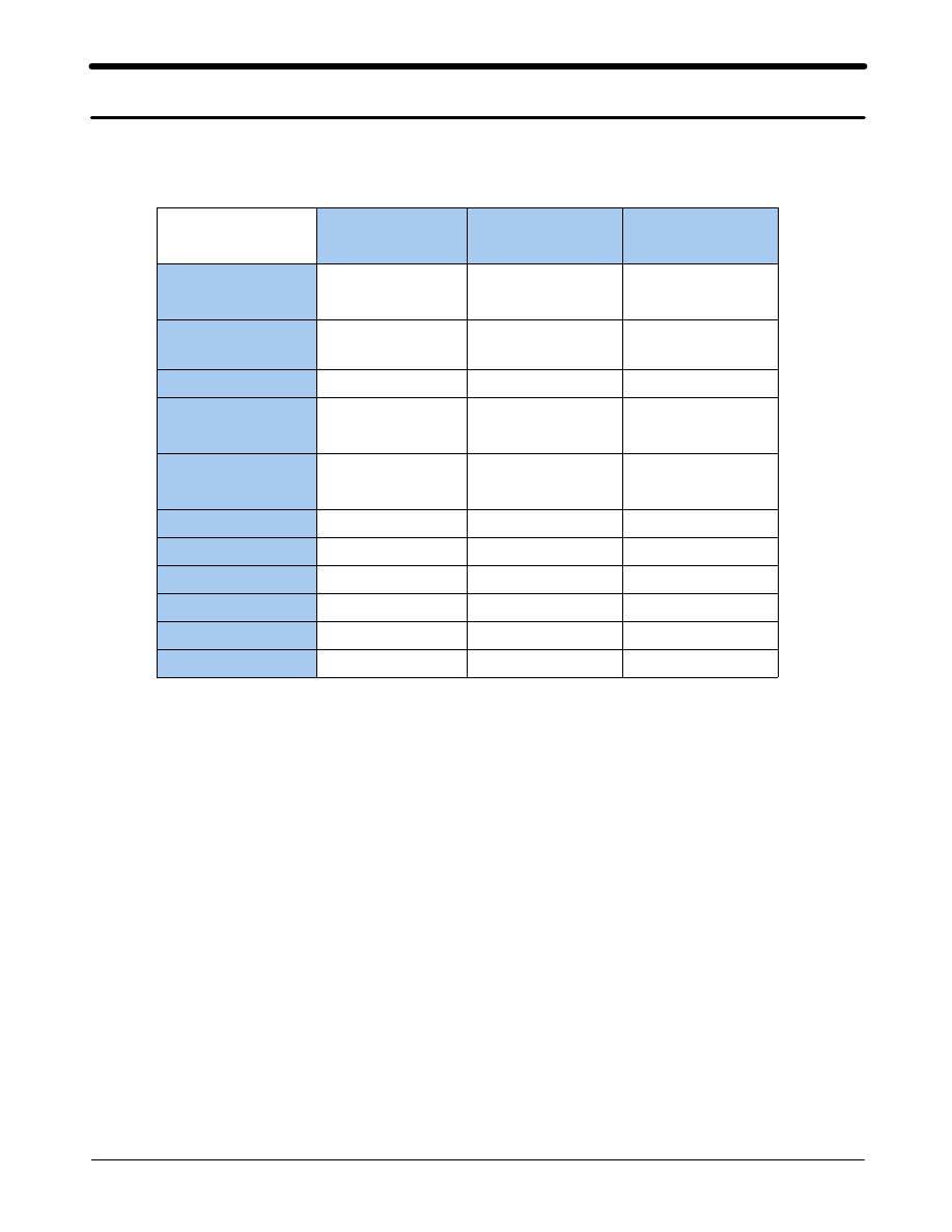
1. SGH-E710 Specification
This Document can not be used without Samsung's authorization
1-1
GSM900
Phase 1
EGSM900
Phase 2
DCS1800
Phase 1
Freq. Band[MHz]
Uplink/Downlink
890~915
935~960
880~915
925~960
1710~1785
1805~1880
ARFCN Range
1~124
0~124 &
975~1023
512~885
Tx/Rx Spacing
45MHz
45MHz
95MHz
Mod. Bit Rate/
Bit Period
270.833KHz
3.692us
270.833KHz
3.692us
270.833KHz
3.692us
Time Slot Period
/Frame Period
576.9us
4.615ms
576.9us
4.615ms
576.9us
4.615ms
Modulation
0.3GMSK
0.3GMSK
0.3GMSK
MS Power
33dBm~13dBm
33dBm~13dBm
33dBm~13dBm
Power Class
5pcl~15pcl
5pcl~19pcl
0pcl~15pcl
Sensitivity
-102dBm
-102dBm
-100dBm
TDMA Mux
8
8
8
Cell Ridius
35Km
35Km
2Km
1. GSM General Specification
SAMSUNG Proprietary-Contents may change without notice
SGH-E710 Specification
1-2
This Document can not be used without Samsung's authorization
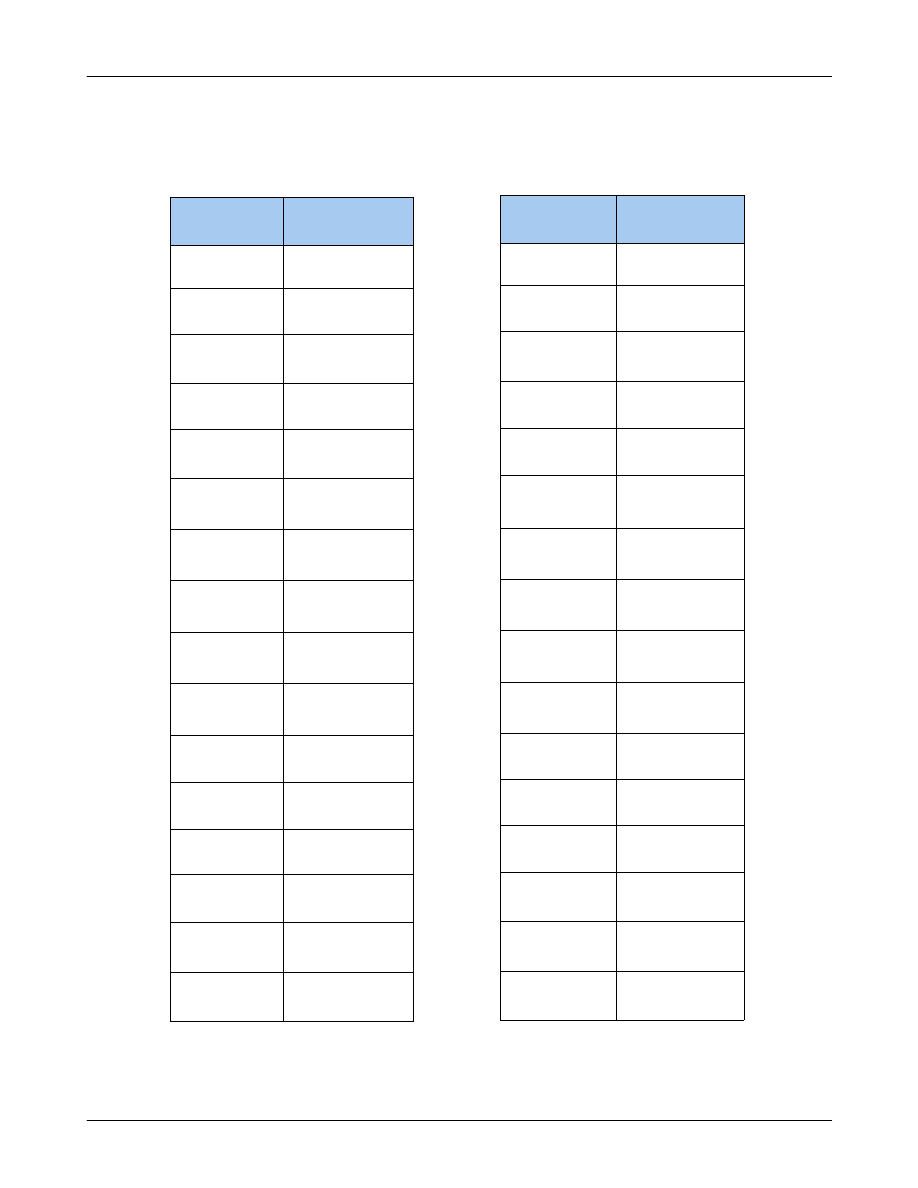
2. GSM TX power class
TX Power
Control Level
GSM900
5
33±2dBm
6
29±2dBm
7
27±2dBm
8
25±2dBm
9
23±2dBm
10
21±2dBm
11
19±2dBm
12
17±2dBm
13
15±2dBm
14
13±2dBm
15
11±2dBm
16
9±3dBm
17
7±3dBm
18
5±3dBm
19
3±3dBm
TX Power
Control Level
DCS1800
0
30±3dBm
1
28±3dBm
2
26±3dBm
3
24±3dBm
4
22±3dBm
5
20±3dBm
6
18±3dBm
7
16±3dBm
8
14±3dBm
9
12±4dBm
10
10±4dBm
11
8±4dBm
12
6±4dBm
13
4±4dBm
14
2±5dBm
15
0±5dBm
SAMSUNG Proprietary-Contents may change without notice
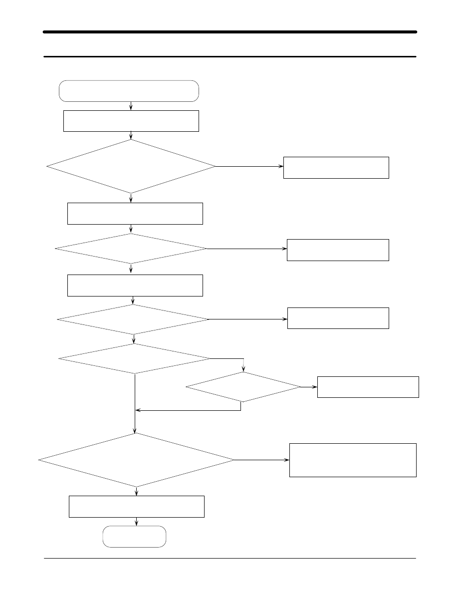
2. SGH-E710 Flow Chart of Troubleshooting
2-1
This Document can not be used without Samsung's authorization
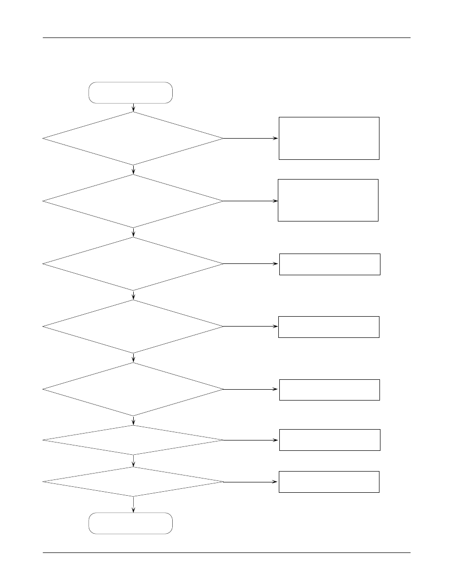
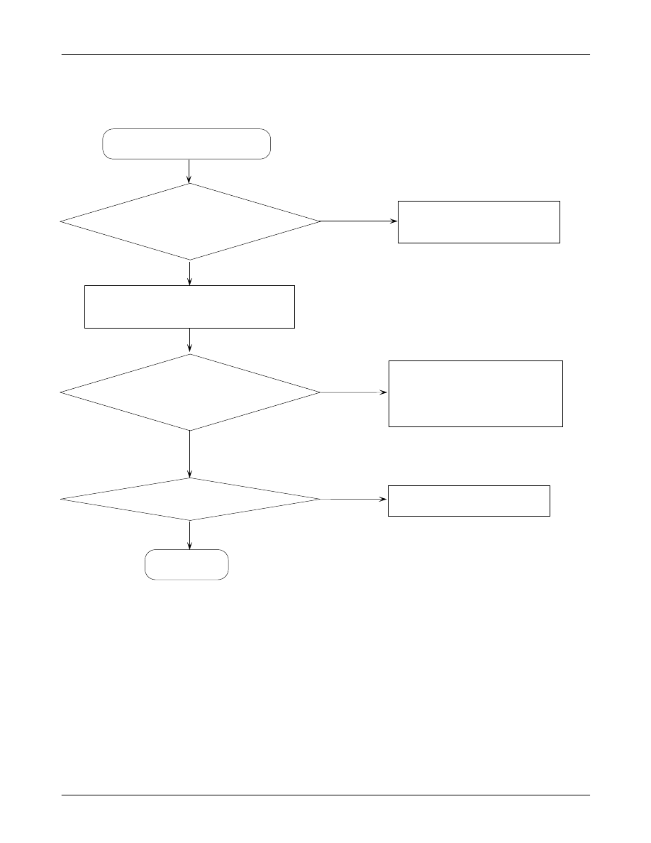
1. Power ON
'Power ON' Does not work
Check the current consumption
Current consumption
≥100mA ?
Check the V bat. voltage
Down load again
Voltage ≥ 3.3V ?
Check the pin of U100
pin #11 ≥ 2.8V ?
Pin #9=1.8V?
Check the Initial operation
END
pin #39 and #33 = 2.8V
Charge the Battery
Check the clock generation
circuit (OSC400, U402 pin#4)
Check the clock signal
at pin #3 of OSC400
Freq.=13MHz,Vrms 300mV
Check U100 and C109
Check U100 and C110
NO
NO
NO
NO
NO
NO
YES
YES
YES
YES
YES
YES
SAMSUNG Proprietary-Contents may change without notice
SGH-E710 Flow Chart of Troubleshooting and Circuit Diagrams
2-2
This Document can not be used without Samsung's authorization
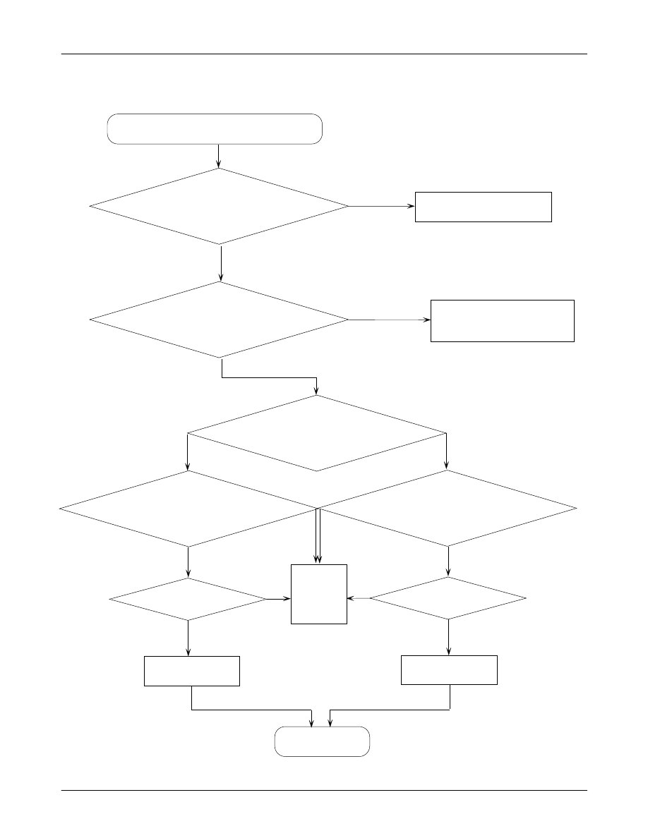
2. System Initial
The pin #9 of U100 = 1.8V
and pin #11 of U100=2.8V?
Initial Failure
Is the pin #19 of U100
" Low --> High" ?
There is 32.768KHz wave
form at the C324, C325 ?
Is the pin #25 of U100
is High ?
The voltage is "High"
at the C106,C112,C113 ?
LCD Display OK ?
Sound operation OK ?
END
Check the U303
Check the U300
Check the U100
Check the LCD part
Check the Audio part
YES
NO
NO
NO
NO
YES
YES
YES
YES
YES
NO
NO
NO
YES
Check the U100
(If it has some problem,
it has to be replaced.)
Check the U100
(If it has some problem,
it has to be replaced.)
SAMSUNG Proprietary-Contents may change without notice
SGH-E710 Flow Chart of Troubleshooting and Circuit Diagrams
2-3
This Document can not be used without Samsung's authorization
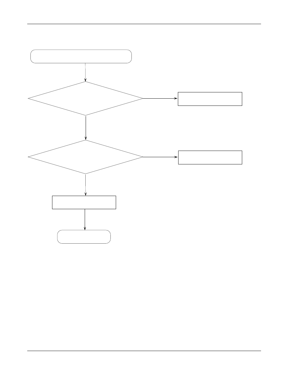
3. SIM Part
Is there any signal
pin #52,53,54 of U100 ?
Check the U303
"Insert SIM" is displayed on the LCD
END
Check the SIM Card
YES
NO
NO
YES
Is there any signal
pin #1,2,3,6 of CN100 ?
Check the U100
SAMSUNG Proprietary-Contents may change without notice
SGH-E710 Flow Chart of Troubleshooting and Circuit Diagrams
2-4
This Document can not be used without Samsung's authorization
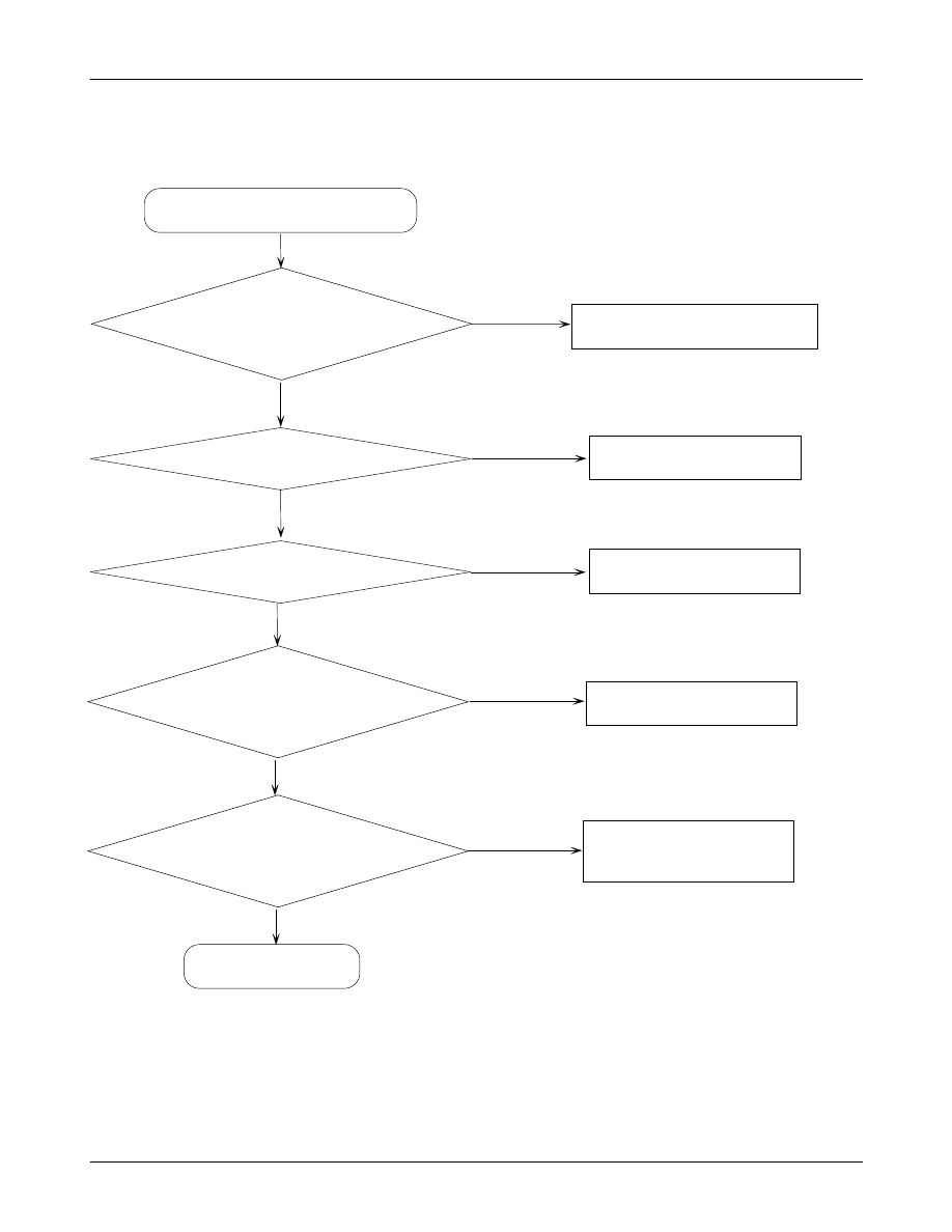
4. Charging Part
The pin #17,18 of CN101
(VEXT) is 5V ?
Replace TA or check CN101
Abnormal charging operation
END
Check the U102
YES
NO
NO
The pin#2 of U102 is Low?
YES
The pin#3 of U102 is Low?
YES
Check the U102
NO
The pin#5 of U101 is
3.2~4.2V?
Check the U101
NO
The ICHRG =1V(during charging)
& 180mV(full charging)?
YES
YES
Solder again or change
R119
NO
SAMSUNG Proprietary-Contents may change without notice
SGH-E710 Flow Chart of Troubleshooting and Circuit Diagrams
2-5
This Document can not be used without Samsung's authorization
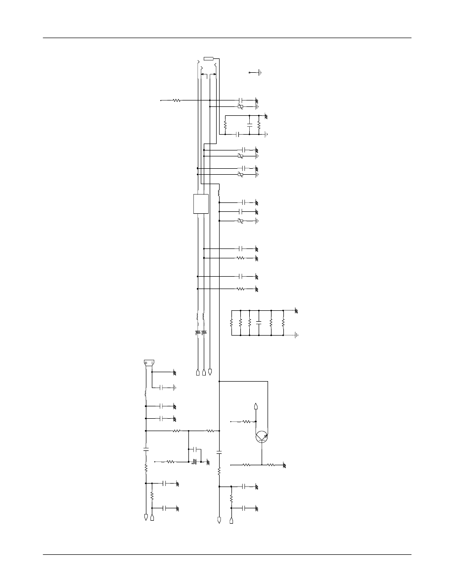
100N F
C105
C103
470N F
VRF
10U F
10V
R120
47K,1%
Q102
DTC144EM
1
3
2
C116
100PF
C115
C107
10U F
10V
3K
2.2U F
C111
R121
12
VRTC
48
V
S
I M
VLDO_1
11
VLDO_2
VLDO_3
39
37
VLDO_4
33
VLDO_5
VLDO_6
42
VLDO_7 40
30
V
R
E
F
34
VDD5
41
VDD67
VEXT
1
4
V
IB
_
D
R
V
VL4S_A
36
35
VL4S_B
VL5S_A
32
31
VL5S_B
9
49
UP_CLK
53
52 UP_IO
54
UP_RST
3 VACC
2 VBA T
VDD12
10
38
VDD34
5
55 RING_PW M
RTC_ALM N
13
17
SCLK
15
SDI
16
SDO
50
S
IM
_
C
L
K
S
IM
_I
O
51
S
IM
_
R
S
T
14
L
E
D
1_
D
R
V
78
L
E
D
2_
D
R
V
20 PSW1_BUF
PWR_KEEP
21
46
PWR_SW1N
PWR_SW 2
47
19
RESETN
R
IN
G
_
D
R
V
6
2
G
N
D
G
N
D
6
3
6
4
G
N
D
6
5
G
N
D
G
N
D
6
6
GNDD
60
6
G
N
D
D
1
G
N
D
Q
28
INTRQ
26
27
EN_5B
57
GN D
6
7
G
N
D
G
N
D
6
8
GN D
58
59
GN D
G
N
D
6
1
56
43
BTEM P
C
R
E
F
29
CSN
18
EN_3
22
23
EN_4[0]
EN_4[1]
24
25
EN_5
EN_5A
U100
44 ADC_AUX1
ADC_AUX2
45
ADC_TRIG
1
3
2
Q100
C100
33PF
G
89
GG
10
VRTC
VBAT
1
1
2 2
3
3
4
4
5
5
6
6
7
G
1.2K
CN100
VCC
A
R115
VPAC
10K,1%
R118
C109
2.2UF
VCC B
2.2U F
C112
2.2U F
C106
DRIVE
6
GND
2
1 ISENSE
PRO G 4
3 VCC
5
VSENSE
U101
R11 0
390K
VRTC
10K,1%
R119
C102
33PF
2
N
E
G
1
P
O
S
M1
VCC
D
VCC_1.8A
R114
330K
C117
10UF
10V
VBAT
C104
100NF
1
4
U103
2
5
6
3
C108
C114
2.2U F
VOSC
470NF
C113
10U F
10V
C101
33PF
VBA T
C110
2.2U F
2
5
6
4
Q101
3
1
VREF
BACKLIGHT1
BACKLIGHT2
RST
RTCALAR M
PWR_KEEP
EN_VPAC
XOEN
A
UP_SDI
UP_SCLK
UP_CS
TA_VEXT
CHG_O
N
SIMCLK
SIMRST
SIMDATA
KEY_ROW(0)
KEY_COL(2)
CHG_DET
PWR_O N
JIG_ON
EN_VRF
ICHRG
TA_VEXT
TA_VEXT
SAMSUNG Proprietary-Contents may change without notice
SGH-E710 Flow Chart of Troubleshooting and Circuit Diagrams
2-6
This Document can not be used without Samsung's authorization
5. Microphone Part
Micro-phone does not work
Is the assembled status of
Microphone O.K?
YES
Reassemble the microphone
NO
Check the DC bias voltage on
Mic path.
The voltage of C237 is
2.2V±10%?
NO
Solder the microphone again
or Replace
C230,C237,R217,R218,R219
Is microphone OK?
NO
Check U300
END
YES
YES
SAMSUNG Proprietary-Contents may change without notice
SGH-E710 Flow Chart of Troubleshooting and Circuit Diagrams
2-7
This Document can not be used without Samsung's authorization
6. Speaker Part
Is the terminal of speaker
is O.K?
NO
Replace the speaker
Are there any signal
at the pin #40,42 of CN200?
NO
Check the LCD module
& Replace CN200
There is no sound from speaker
YES
YES
The type of sound from
the speaker is Melody?
YES
NO
Are there any signal
at the pin #5,7 of U201?
Are there any signal
at the pin #3,9 of U201?
Check
U201,
U303
NO
NO
Pin #4 of U201
is Low?
Pin #4 of U201
is High?
Check U202
Check U300
NO
NO
YES
YES
YES
YES
END
SAMSUNG Proprietary-Contents may change without notice
SGH-E710 Flow Chart of Troubleshooting and Circuit Diagrams
2-8
This Document can not be used without Samsung's authorization
JA
C
K
_
IN
E
A
R
_
S
P
K
_
P
E
A
R
_
M
IC
_
P
E
A
R
_
S
P
K
_
N
E
A
R
_
M
IC
_N
R
23
8
0
C
2
61
3
9P
F
R
2
4
1
N
C
R
2
1
9
R
2
4
0
N
C
51
K
1
.2
K
R
2
35
R
22
3
4
.7
K
ZD
20
3
8
P
F
C
23
4
1
U
F
C
23
0
8
20
P
F
R
2
2
9
1
N
F
C
2
49
C
2
40
3
3U
F
C
2
36
3
3U
F
6
.3
V
6
.3
V
39
P
F
C
24
3
C
23
9
1
U
F
1K
R
23
0
82
K
,1
%
R
23
1
V
C
C
A
R
23
9
0
R
23
7
0
47
0n
F
C
23
8
39
P
F
3
3U
F
C
2
37
C
26
0
4.
7K
R
22
1
8
2P
F
C
2
45
1
K
R
2
3
3
1
K
R
23
2
T
H
2
00
L
2
0
0
1
00
n
H
ZD
201
C
2
42
18
0
P
F
C
2
48
1N
F
R
2
25
10
K
33
P
F
C
2
44
ZD
202
V
C
C
D
R
2
28
56
0
P
F
M
A
IN
_
M
IC
4
7K
,1
%
R
2
18
3
1
R
21
7
10
K
Q
20
0
2
33
P
F
C
24
1
C
2
47
3
3P
F
5
6
ZD
200
C
N
20
1
1
2
3
4
3
9P
F
C
2
33
R
2
2
0
1
00
K
N
C
0
R
22
6
4
7
K
,1
%
R
23
4
R
22
7
1N
F
C
24
6
1
0
0n
H
L
20
1
1
1
2
2
3
3
4
4
F
2
0
0
C
2
32
1
N
F
R
22
2
V
C
C
A
10
0
n
H
R
22
4
10
0n
H
V
C
C
A
33
P
F
C
23
5
A
U
X
IN
JA
C
K
_I
N
E
A
R
_
S
W
IT
C
H
A
O
U
T
B
P
A
O
U
T
B
N
A
U
X
O
U
T
M
IC
O
U
T
M
IC
IN
SAMSUNG Proprietary-Contents may change without notice
SGH-E710 Flow Chart of Troubleshooting and Circuit Diagrams
2-9
This Document can not be used without Samsung's authorization
7. Camera Part
Camera function does not work
Check the connect CN200?
NO
Connect the CN200
Pin #9 of U203 = 2.8V?
NO
NO
Pin#3 of OSC200 is 25MHz?
NO
Pin #10 of U203 = 2.8V?
Check
U200
END
YES
YES
YES
YES
Pin#1 of OSC200 = High?
NO
Pin #2 of U203 = High?
YES
Check the U203
Check
U303
NO
NO
Pin#54 of CN200 is High?
Check solder status of
R207, C208
Replace the OSC200
YES
SAMSUNG Proprietary-Contents may change without notice
SGH-E710 Flow Chart of Troubleshooting and Circuit Diagrams
2-10
This Document can not be used without Samsung's authorization
8. EGSM Receiver
Continuous RX ON
RF Input : 62 CH
AMP : -50dBm
NORMAL CONDITION
Catch the channel ?
YES
NO
F400 Check
Pin #6 ≥ -65dBm ?
F400 Check
Pin #11 ≥ -65dBm ?
U401 Check
Pin#20,21 ≥ -65dBm ?
Check soldered status of
C400,402
CN400
Resolder or Change
F400 Resolder or Change
U401 Check
Pin#9,32=Clean 2.8V?
U401 Check
Pin#28,1,2,3=100mV?
U100,C106,C112
Check or resolder
Check U300
NO
NO
YES
YES
YES
YES
NO
YES
U401 Check
Pin #8 : 13MHz ?
Vpp : 860mV?
OSC400 Check
Pin #8 : 13MHz ?
Vpp : 950mV?
OSC400 Check
Pin #4 = 2.8V ?
U401
Change or resolder
NO
NO
NO
R412,C426
resolder
OSC400
Change or resolder
YES
YES
YES
NO
Check soldered status of
C415,417,L406,F403
F403 Check
Pin #1 ≥ -65dBm ?
Check soldered status of
L410 &
F400 Resolder or Change
NO
YES
NO
SAMSUNG Proprietary-Contents may change without notice
SGH-E710 Flow Chart of Troubleshooting and Circuit Diagrams
2-11
This Document can not be used without Samsung's authorization
9. EGSM Transmitter
Continuous TX ON condition
TX Power Code : 500 code Applied
CH : 62
RBW : 100KHz
VBW : 100KHz
SPAN : 10MHz
REF. Level : 10dBm
ATT. : 20dB
C403
= 3.7V?
Change U400
NO
YES
F400 Pin#6
About 2~3 dBm?
F400
Pin#10 = High?
U300,301
Check & Change
NO
C402,CN400
Check & Change
YES
F400
Check & Change
YES
Check the
Battery Block
Level of
U400 Pin #6 is
1.2V?
Check
& Change R406
OK ?
U300
Check & Change
YES
YES
NO
NO
NO
NO
U400 pin#7
About -5 dBm?
U400 pin#3
High ?
Check U300
YES
NO
YES
U401 Check
Pin#9,32 ≥ 2.8V ?
U401 Check
Pin #8 : 13MHz ?
Vpp : 860mV?
OSC400 Check
Pin #8 : 13MHz ?
Vpp : 950mV?
OSC400 Check
Pin #4 = 2.8V ?
NO
YES
NO
NO
NO
R412,C426
resolder
OSC400
Change or resolder
YES
YES
YES
NO
U100,C106,C112
Check or resolder
U401 Pin
#4,5,6,7 = 1.7V?
YES
Change U400
Check U300
NO
YES
Level of
F400 Pin#7 is
4~5dBm ?

SAMSUNG Proprietary-Contents may change without notice
SGH-E710 Flow Chart of Troubleshooting and Circuit Diagrams
2-12
This Document can not be used without Samsung's authorization
10. DCS Receiver
Continuous RX ON
RF Input : 660 CH
AMP : -50dBm
NORMAL CONDITION
Catch the channel ?
YES
NO
F400 Check
Pin #6 ≥ -65dBm ?
F400 Check
Pin #3 ≥ -65dBm ?
U401 Check
Pin#18,19 ≥ -65dBm ?
Check soldered status of
C400,402
CN400
Resolder or Change
F400 Resolder or Change
U401 Check
Pin#9,32=Clean 2.8V?
U401 Check
Pin#28,1,2,3=100mV?
U100,C106,C112
Check or resolder
Check U300
NO
NO
YES
YES
YES
YES
NO
YES
U401 Check
Pin #8 : 13MHz ?
Vpp : 860mV?
OSC400 Check
Pin #8 : 13MHz ?
Vpp : 950mV?
OSC400 Check
Pin #4 = 2.8V ?
U401
Change or resolder
NO
NO
NO
R412,C426
resolder
OSC400
Change or resolder
YES
YES
YES
NO
Check soldered status of
C407,414,L405,F402
F402 Check
Pin #1 ≥ -65dBm ?
Check soldered status of
L410,C430
NO
YES
NO
SAMSUNG Proprietary-Contents may change without notice
SGH-E710 Flow Chart of Troubleshooting and Circuit Diagrams
2-13
This Document can not be used without Samsung's authorization
11. DCS Transmitter
Continuous TX ON condition
TX Power Code : 350 code Applied
CH : 660
RBW : 100KHz
VBW : 100KHz
SPAN : 10MHz
REF. Level : 10dBm
ATT. : 20dB
C403
= 3.7V?
Change U400
NO
YES
F400 Pin#6
About 2~3 dBm?
F400
Pin#4 = High?
U300,302
Check & Change
NO
C402,CN400
Check & Change
Level of
F400 Pin#5 is
4~5dBm ?
YES
F400,L401,C408,C410
Check & Change
YES
Check the
Battery Block
Level of
U400 Pin #6 is
1.2V?
Check
& Change R406
OK ?
U300
Check & Change
YES
YES
NO
NO
NO
NO
U400 pin#1
About -5 dBm?
U400 pin#3
High ?
Check U300
YES
NO
YES
U401 Check
Pin#9,32 ≥ 2.8V ?
U401 Check
Pin #8 : 13MHz ?
Vpp : 860mV?
OSC400 Check
Pin #8 : 13MHz ?
Vpp : 950mV?
OSC400 Check
Pin #4 = 2.8V ?
NO
YES
NO
NO
NO
R412,C426
resolder
OSC400
Change or resolder
YES
YES
YES
NO
U100,C106,C112
Check or resolder
U401 Pin
#4,5,6,7 = 1.7V?
YES
Change U400
Check U300
NO
YES
SAMSUNG Proprietary-Contents may change without notice
SGH-E710 Flow Chart of Troubleshooting and Circuit Diagrams
2-14
This Document can not be used without Samsung's authorization
L
40
9
22
P
F
1.
5n
H
L
40
8
C
41
4
2.
2
P
F
V
R
F
L
40
0
5
.6
n
H
C
43
0
L
40
6
27
n
H
L
41
0
N
C
XE
N
26
XIN
8
XO
UT
27
10
_P
DN
_S
EN
12
47
P
F
SD
I
14
SD
O
11
T
X
IN
5
T
X
IP
4
T
X
Q
N
7
6
T
X
Q
P
9
VD
D
32
VD
D
17
R
F
IP
P
16
RF
OD
22
RF
OG
23
R
X
IN
3
2
R
X
IP
1
R
X
Q
N
28
RX
QP
SC
LK
13
G
N
D
36
37
N
C
N
C
38
R
F
ID
N
19
R
F
ID
P
18
R
F
IG
N
21
20
R
F
IG
P
R
F
IP
N
24
DIA
G2
25
G
N
D
15
GN
D29
30
GN
D
31
GN
D
GN
D3
3
GN
D3
4
35
G
N
D
U
40
1
DIA
G1
V
P
A
C
1.
8P
F
C
40
5
C
40
4
10
N
F
V
R
F
22
N
F
C
41
9
R
40
1
82
0
22
0
R
40
4
3
G
1
4
G
2
C
N
40
0
10
0K
R
40
6
0.
5P
F
C
43
1
N
C
C
42
9
C
41
7
G
6
G
8
G
12
P
C
S
R
X
3
2
VC
1
VC
2
4
10
VC
3
0.
75
P
F
F
40
0
9
AN
T
1
D
C
S
R
X
D
C
S
/P
C
S
T
X
5
11
E
G
S
M
R
X
E
G
S
M
T
X
7
6
V
R
A
M
P
V
R
E
G
5
1P
F
C41
3
7
9
11
P
C
S
O
U
T
3T
X
E
N
4
V
B
A
T
T
10
VC
C
VC
C2
81
2
VC
C2
R
F
31
40
U
40
0
2
B
A
N
D
D
C
S
IN
1
13
G
N
D
C
41
6
10
0P
F
C
41
8
1U
F
R
40
5
2
G
5
G
IN
1
3
O
U
T
O
U
T
4
27
0
2
G
G
5
IN
1
3
O
U
T
O
U
T
4
F
40
2
15
R
40
3
F
40
3
R
40
2
82
0
10
R
40
0
G
25
G
1
IN
3
O
U
T
O
U
T
4
10
0N
F
F
40
1
0.
5P
F
C
41
0
C
42
8
L
40
1
2.
7n
H
5.
6n
H
L
40
2
C
40
6
1.
8P
F
27
0P
F
1.
0n
H
C
40
0
C
40
9
L
40
3
0
V
B
A
T
0.
75
P
F
C
40
8
A
N
T
C
40
3
10
0U
F
6.
3V
A
N
T
1
C
40
1
1P
F
C
41
5
0.
75
P
F
33
P
F
C
41
1
47
P
F
C
40
2
C
41
2
1N
F
2.
2P
F
L
40
5
6.
8n
H
N
C
C
40
7
L
40
4
P
C
S
_L
N
A
_I
N
_P
D
C
S
_T
X
_E
N
G
S
M
_T
X
_E
N
D
C
S
_L
N
A
_I
N
_N
D
C
S
_L
N
A
_I
N
_P
P
C
S
_L
N
A
_I
N
_P
P
C
S
_L
N
A
_I
N
_N
D
C
S
_L
N
A
_I
N
_P
D
C
S
_L
N
A
_I
N
_N
G
S
M
_L
N
A
_I
N
_N
G
S
M
_L
N
A
_I
N
_P
P
C
S
_R
X
_E
N
P
C
S
_L
N
A
_I
N
_N
S
E
R
D
A
T
S
I_
E
N
S
E
R
L
E
R
X
IN
R
X
Q
P
R
X
Q
N
C
L
K
13
M
_R
F
T
X
IN
T
X
IP
T
X
Q
N
T
X
Q
P
G
S
M
_L
N
A
_I
N
_N
G
S
M
_L
N
A
_I
N
_P
G
S
M
_P
A
M
_I
N
D
P
C
S
_P
A
M
_I
N
S
E
R
C
L
K
T
X
P
O
W
E
R
T
X
_B
A
N
D
_S
E
L
G
S
M
_P
A
M
_I
N
D
P
C
S
_P
A
M
_I
N
T
X
_E
N
R
X
IP
SAMSUNG Proprietary-Contents may change without notice
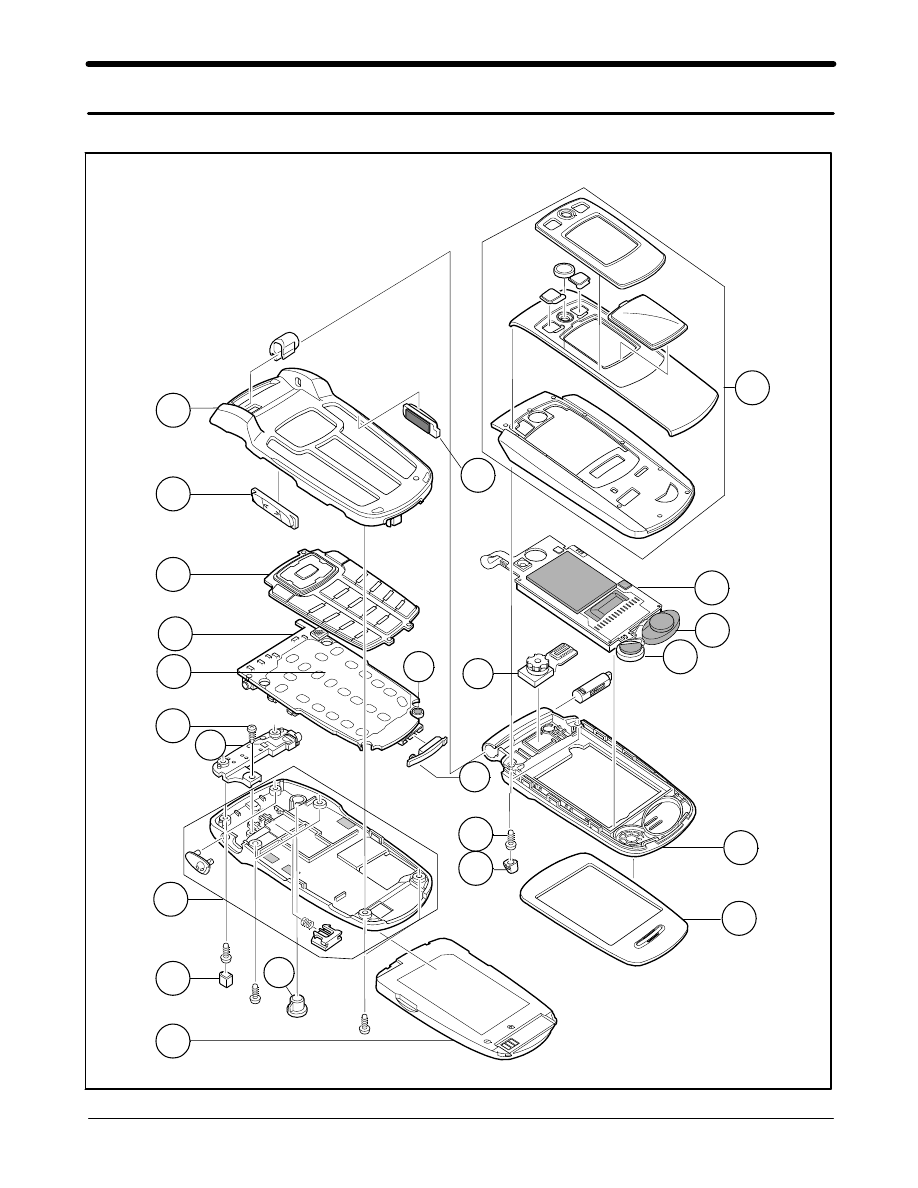
3. SGH-E710 Exploded View and its Parts list
3-1
This Document can not be used without Samsung's authorization
1. Cellular phone Exploded View
1
2
3
4
5
6
7
8
9
11
12
13
14
18
19
21
22
23
10
16
15
20
17
SAMSUNG Proprietary-Contents may change without notice
SGH- E710 Exploded view and its Part list
3-2
This Document can not be used without Samsung's authorization
2. Cellular phone Parts list
Location
NO.
Description
SEC.CODE
Remark
1
FOLDER UPPER ASS'Y
GH75-03786D
2
LCD
GH07-00406A
3
SPEAKER
3001-001446
4
MOTOR
3101-001370
5
CAMERA
GH59-00959A
6
FOLDER LOWER
GH75-03263A
7
WINDOW LCD
GH75-03785A
8
SCREW
6001-001478
9
FOLDER LOWER SCREW CAP LEFT
GH73-02160A
FOLDER LOWER SCREW CAP RIGHT
GH73-02161A
10
IF COVER
GH72-08382A
11
CAMERA KEY
GH75-03586A
12
FRONT COVER
GH75-03261F
13
VOLUME KEY
GH75-03256A
14
KEYPAD
GH75-03688D
15
MAIN PBA
GH92-01592A
16
DOME SHEET
GH59-00895A
17
MIC
GH30-00032A
18
SCREW
6001-001478
19
INTENNA
GH42-00317A
20
REAR COVER
GH75-03264A
21
REAR SCREW COVER
GH73-02152A
22
RF COVER
GH73-02524A
23
BATTERY
GH43-01026B
SAMSUNG Proprietary-Contents may change without notice
SGH-E710 Exploded view and its Part list
3-3
This Document can not be used without Samsung's authorization
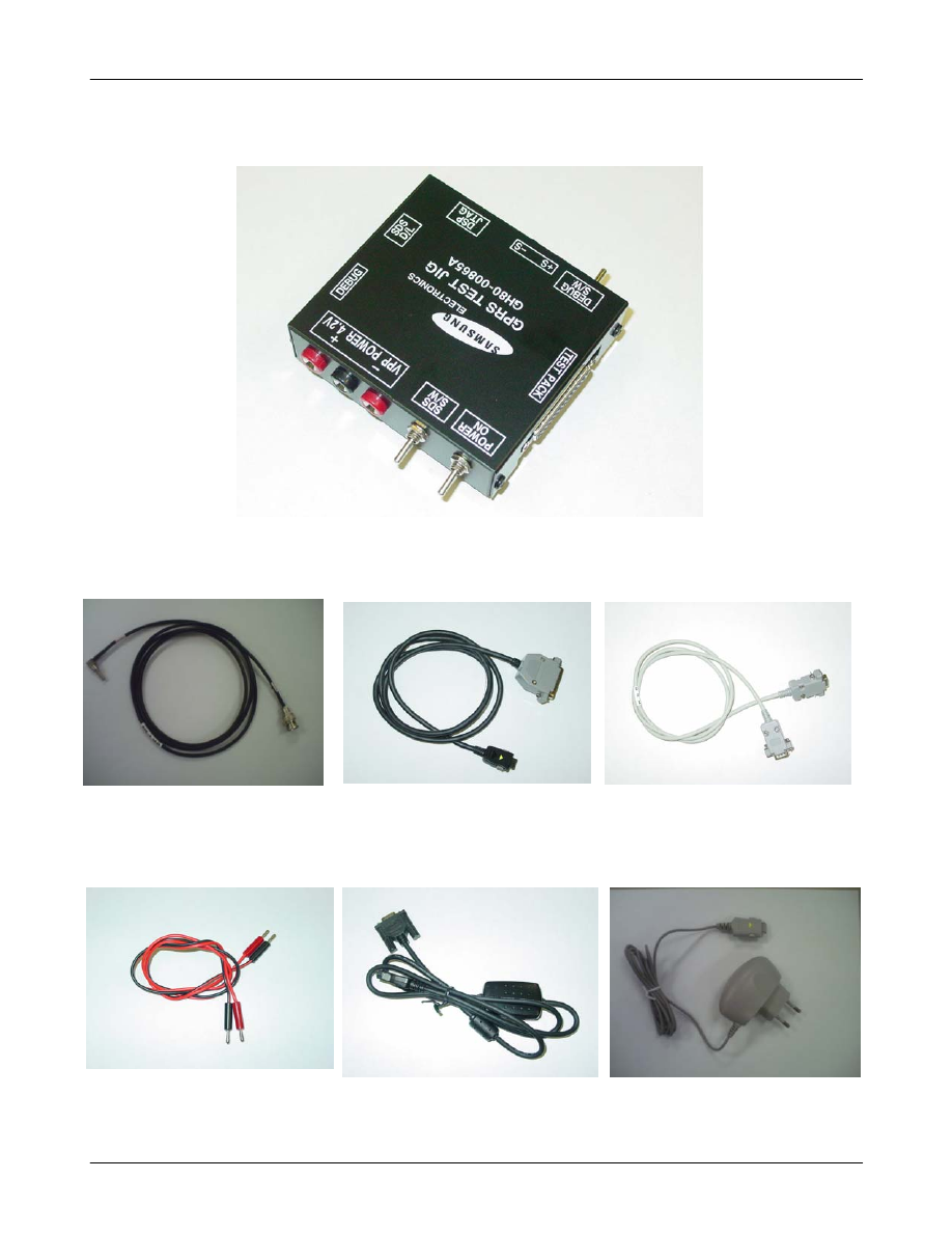
3. Test Jig (GH80-00865A)
3-1. RF Test Cable
(GH39-00182A)
3-2. Test Cable
(GH39-00127A)
3-3. Serial Cable
3-4. Power Supply Cable
3-5. DATA CABLE
(GH39-00159A)
3-6. TA
(GH44-00482A)
SAMSUNG Proprietary-Contents may change without notice
4. SGH-E710 MAIN Electrical Parts List
4-1
This Document can not be used without Samsung's authorization
SEC Code
Design LOC
GH92-01592A
GH41-00451A
GH96-01380A
GH30-00032A
GH59-00895A
GH68-02026A
GH73-02484A
GH74-06321A
GH74-06775A
2203-000812
C100
2203-000812
C101
2203-000812
C102
2203-001652
C103
2203-005061
C104
2203-005061
C105
2203-006201
C106
2404-001268
C107
2203-001652
C108
2203-006201
C109
2203-006201
C110
2203-005796
C111
2203-006201
C112
2404-001268
C113
2203-006201
C114
2203-000233
C115
2404-001268
C116
2404-001268
C117
2203-005065
C118
2203-005061
C119
2203-000995
C120
2203-006090
C121
2203-006208
C131
2203-005061
C200
2203-005061
C206
2203-005509
C207
2203-005496
C208
2203-000812
C210
2203-005061
C211
2203-000254
C212
SEC Code
Design LOC
2203-000233
C213
2203-000254
C214
2203-005061
C215
2203-006093
C216
2203-000233
C217
2203-006201
C218
2203-000233
C219
2203-000654
C220
2404-001086
C221
2203-005061
C222
2203-001405
C223
2203-005061
C224
2203-006090
C225
2203-006090
C226
2203-000254
C227
2404-001086
C228
2203-005061
C229
2203-006093
C230
2203-000438
C231
2203-000438
C232
2203-000995
C233
2203-001259
C234
2203-000812
C235
2404-001151
C236
2404-001151
C237
2203-006257
C238
2203-005065
C239
2404-001151
C240
2203-000812
C241
2203-005503
C242
2203-000854
C243
2203-000812
C244
2203-001239
C245
2203-000438
C246
2203-000812
C247
2203-000438
C248
2203-000438
C249
2503-001045
C250
2503-001045
C251
SEC Code
Design LOC
2503-001045
C252
2503-001045
C253
2503-001045
C254
2503-001045
C255
2203-006093
C256
2203-000812
C257
2203-000812
C258
2203-000812
C259
2203-000995
C260
2203-000854
C261
2203-005061
C300
2203-001405
C301
2203-000254
C302
2203-000254
C303
2203-005496
C304
2203-000679
C305
2203-000254
C306
2203-005061
C307
2203-000233
C308
2203-006093
C309
2203-005450
C310
2203-005496
C311
2203-000254
C312
2203-000254
C313
2203-005061
C314
2203-000233
C315
2203-000254
C316
2203-000254
C317
2203-000254
C318
2203-000254
C319
2203-005052
C320
2203-000995
C321
2203-000233
C322
2203-005482
C323
2203-000628
C324
2203-000628
C325
2203-000233
C326
2203-000233
C327
2203-000254
C328
SAMSUNG Proprietary-Contents may change without notice
SGH-E710 Electrical Parts List
4-2
This Document can not be used without Samsung's authorization
SEC Code
Design LOC
2203-005061
C329
2203-000254
C330
2203-005061
C331
2203-005496
C332
2203-005480
C333
2203-000940
C334
2203-000254
C335
2203-005061
C336
2203-000679
C337
2203-000679
C338
2203-000233
C339
2703-001749
C400
2203-001385
C401
2203-000995
C402
2404-001134
C403
2203-000254
C404
2203-005050
C405
2203-005050
C406
2203-005552
C407
2203-002677
C408
2203-000654
C409
2203-002668
C410
2203-000812
C411
2203-000438
C412
2203-000466
C413
2203-005552
C414
2203-002677
C415
2203-000233
C416
2203-002677
C417
2203-006093
C418
2203-006137
C419
2203-000278
C420
2203-000438
C421
2203-000438
C422
2203-000233
C423
2203-000233
C424
2203-000254
C425
2203-000254
C426
2203-000254
C427
SEC Code
Design LOC
2203-005061
C428
2203-002668
C429
3709-001187
CN100
3710-001866
CN1006
3710-001611
CN101
3711-005397
CN200
3722-002067
CN201
3705-001287
CN400
2901-001271
F200
2909-001213
F400
2904-001450
F401
2904-001419
F402
2904-001417
F403
2703-002313
L200
2703-002313
L201
2703-001748
L400
2703-001737
L401
2703-002665
L402
2007-000171
L403
2703-002547
L405
2703-001907
L406
3301-001105
L407
2703-002369
L408
2203-000628
L409
2203-000995
L410
0604-001261
LED100
0601-001790
LED101
0601-001790
LED102
0601-001790
LED103
0601-001790
LED104
0601-001790
LED105
0601-001790
LED106
0601-001790
LED107
0601-001790
LED108
0601-001790
LED109
0601-001790
LED110
0601-001790
LED111
0601-001790
LED112
4302-001130
M1
SEC Code
Design LOC
2804-001577
OSC200
2801-004025
OSC300
2809-001260
OSC400
0504-001113
Q100
0502-001201
Q101
0504-001113
Q102
0501-000225
Q200
0504-001141
Q300
0504-001141
Q301
0504-001141
Q302
2007-000157
R100
2007-000157
R101
2007-000157
R102
2007-000157
R103
2007-000140
R104
2007-000140
R105
2007-000140
R106
2007-000140
R107
2007-000140
R108
2007-000140
R109
2007-000167
R110
2007-000140
R111
2007-000140
R112
2007-000140
R113
2007-000758
R114
2007-001319
R115
2007-001301
R116
2007-001291
R117
2007-007142
R118
2007-007142
R119
2007-007139
R120
2007-001323
R121
2007-000171
R122
2007-000171
R123
2007-000171
R124
2007-000171
R125
2007-000171
R126
2007-000171
R127
2007-000171
R128
SAMSUNG Proprietary-Contents may change without notice
SGH-E710 Electrical Parts List
4-3
This Document can not be used without Samsung's authorization
SEC Code
Design LOC
2007-000171
R129
2007-001294
R130
2007-001301
R131
2007-001294
R132
2007-001294
R133
2007-001294
R134
2007-001301
R135
2007-001301
R136
2007-001301
R137
2007-001301
R138
2007-000171
R139
2007-001301
R140
2007-000171
R141
2007-001301
R142
2007-001301
R143
2007-000140
R144
2007-000140
R145
2007-000140
R146
2007-000148
R200
2007-000148
R201
2007-000171
R202
2007-000171
R203
2007-000171
R204
2007-000171
R205
2007-000171
R206
2007-007139
R207
2007-002965
R208
2007-000162
R209
2007-002965
R210
2007-000171
R212
2007-007489
R213
2007-000775
R214
2007-000775
R215
2007-001325
R216
2007-000148
R217
2007-007139
R218
2007-001319
R219
2007-000162
R220
2007-000143
R221
SEC Code
Design LOC
2703-002313
R222
2007-000143
R223
2703-002313
R224
2007-000148
R225
2007-000171
R226
2007-007139
R227
2203-002525
R228
2203-001221
R229
2007-007590
R230
2007-000140
R231
2007-000140
R232
2007-000140
R233
2007-007014
R235
2007-000162
R236
2007-000171
R237
2007-000171
R238
2007-000171
R239
2203-000438
R241
2007-002796
R300
2007-000157
R301
2007-007319
R302
2007-000139
R303
2007-000162
R304
2007-007200
R309
2007-007200
R310
2007-000170
R311
2007-000162
R312
2007-000157
R313
2007-000162
R314
2007-007142
R315
2007-000162
R316
2007-007573
R317
2007-007573
R319
2007-000162
R320
2007-007139
R321
2007-000157
R323
2007-000171
R324
2007-000144
R326
2007-000171
R327
SEC Code
Design LOC
2007-000171
R328
2007-000172
R400
2007-001316
R401
2007-001316
R402
2007-002965
R403
2007-000139
R404
2007-001311
R405
2007-000162
R406
2007-000172
R408
2007-000242
R409
2007-002797
R410
2007-000148
R411
2007-000138
R412
2007-000148
R413
3404-001152
SW1
3404-001152
SW2
3404-001152
SW3
1203-002902
U100
1203-002127
U101
1203-001720
U102
0506-001052
U103
GH13-00020A
U200
1001-001183
U201
1204-002161
U202
1203-002861
U203
1204-001984
U300
0504-001042
U301
0504-001042
U302
GH09-00025A
U303
1209-001219
U304
0504-001042
U305
1009-001010
U306
1109-001281
U307
1201-001954
U400
1205-002384
U401
0801-000306
U402
1405-001018
ZD100
1405-001082
ZD101
1405-001082
ZD102
SAMSUNG Proprietary-Contents may change without notice
SGH-E710 Electrical Parts List
4-4
This Document can not be used without Samsung's authorization
SEC Code
Design LOC
1405-001082
ZD103
1405-001082
ZD104
1405-001018
ZD105
1405-001082
ZD106
1405-001082
ZD107
1405-001082
ZD108
1405-001082
ZD109
1405-001082
ZD110
1405-001082
ZD111
1405-001082
ZD112
1405-001082
ZD113
1405-001082
ZD114
1405-001082
ZD115
1405-001082
ZD116
1405-001082
ZD117
1405-001082
ZD121
1405-001082
ZD122
1405-001082
ZD123
1405-001082
ZD124
1405-001082
ZD125
1405-001082
ZD126
1405-001082
ZD127
1405-001082
ZD128
1405-001082
ZD200
1405-001082
ZD201
1405-001082
ZD202
1405-001082
ZD203
SAMSUNG Proprietary-Contents may change without notice
This Document can not be used without Samsung's authorization
5. SGH-E710 Block Diagrams
5-1
1. RF Solution Block Diagram
Drivers
Charger
Power
Mgmt
SIM
Driver
PSC2106
Multi-Function
Power Supply
Trident
II
RTC
Core
Memory I/F
Serial
Control
Power
Keypad
DSP
Memory I/F
System
Clock
P_CTL
R
F
T
r
a
n
c
e
i
v
e
r
S
I
4
2
0
5
RF-BB
I/F
RF-IF
Synthesizer
LNA
IN
Power
AMP I/F
256Mbit
Flash Memory
64Mbit SRAM
System
I/F
LCD I/F
Camera
I/F
CLK
MV317SAQ
CSP1093
Mixed Signal
Processor
DSP
I/F
DAI
Audio
I/F
RF Block
Enable
RF
I/F
Power
I/F
OSC
13MHz
Crystal
32.768
KHz
A[1..23]
D[0..15]
Control
A[0..8]
D[0..15
Control
VRTC
1V8_Core
2V8_DIG
LCD with
Camera
Control
LCD_D[0..15]
Control
C_D[0..7]
LDO
MIC2212
VEP
CAM_VCC
CAMPWR_ON
Sound Gen.
YMU762
CLK13M_RF
CLK13M_MC
CLK13M_TR
CLK13M_YMU
SPK
Analog Switch
MAX4684
RF_EN
MIC
38F3350WWZD
MIC-SPK
Ear-Jack
KEY
PAD
KB_COL[0:4]
KB_ROW[0:4]
2V8_RF
RF_Power_EN
PWR_KEEP
CHG_DET
CHG_ON
I_CHG
CHG Block
LTC1734
I/FC
ON
18P
SIM
CON
SIM_RST
SIM_RST
SIM_CLK
SIM_Data
SIM_Data
SIM_CLK
V_SIM
TA_VEXT
DEBUG
SDS
JIG-ON
DLC_DET
SPK
AFC
TX_PWR
SW_EN
3
TXI_I/O
SER_CTL
TXQ_I/O
TX_EN
V_PAC
GSM
DCS
PCS
TX_BAND_SEL
2
GSM
DCS
PCS
V_BAT
V_BAT
V_BAT
V_BAT
VREF
Backlight
LED
Backlight
Contractor
Antenna
OSC
25MHz
CLK_25MHz
CLK_CTL
ASM
SAW
PAM
SAMSUNG Proprietary-Contents may change without notice
This Document can not be used without Samsung's authorization
6. SGH-E710 PCB Diagrams
6-1
1.Main TOP Diagram
A
N
T1
C100
C
10
1
C
10
2
C
10
3
C104
C105
C106
C107
C
10
8
C
10
9
C
11
0
C111
C112
C113
C114
C115
C116
C117
C118
C
11
9
C
20
0
C
20
1
C
20
2
C
20
3
C
20
4
C
20
5
C
20
6
C
20
8
C
20
9
C
21
0
C
21
1
C
21
2
C
21
3
C214
C215
C
21
6
C
21
7
C
21
8
C
21
9
C
22
0
C221
C222
C
22
3
C224
C225
C226
C227
C
22
8
C
22
9
C
23
0
C
23
1
C
23
2
C
23
3
C
23
4
C
23
5
C
23
7
C
23
8
C
23
9
C
24
2
C
24
3
C244
C
24
5
C
24
6
C250
C251
C252
C253
C254
C255
C
25
6
C
25
7
C
25
8
C
25
9
C260
C
26
1
C
30
0
C
30
1
C
30
2
C303
C304
C305
C306
C
30
7
C
30
9
C
31
0
C311
C
31
2
C
31
3
C
31
4
C
31
5
C
31
6
C
31
7
C
31
8
C
31
9
C
32
0
C322
C
32
4
C
32
5
C326
C327
C
32
8
C
32
9
C330
C331
C332
C
33
3
C
33
4
C
33
5
C336
C
33
7 C338
C
33
9
C
40
0 C401
C
40
2
C
40
3
C
40
4
C
40
5
C
40
6
C
40
7
C408
C409
C410
C411
C
41
2
C413
C
41
4
C415
C
41
6
C417
C418
C419
C420
C
42
1
C422
C
42
3
C
42
4
C
42
5
C
42
6
C
42
7
C
42
8
C429
C430
C
43
1
C
N
10
0
C
N
10
06
C
N
10
1
C
N
20
0
CN201
C
N
40
0
F4
00
F4
01
F4
02
F4
03
G
1
G
2
G
3
G
4
L2
00
L201
L400
L401
L4
02
L4
03
L404
L4
05
L4
06
L4
07
L4
08
L4
09
L4
10
LE
D
10
0
M
1
M
AI
N
_M
IC
OSC200
OSC300
O
SC
40
0
Q100
Q101
Q
10
2
Q200
R
10
0
R
10
1
R
10
2
R103
R104
R105
R106
R107
R
10
8
R109
R110
R111
R112
R113
R114
R115
R
11
6
R
11
7
R118
R119
R
12
0
R121
R
14
4
R145
R
14
6
R
20
0
R
20
1
R
20
2
R
20
3
R
20
4
R
20
5
R
20
6
R
20
7
R
20
8
R
20
9
R
21
0
R
21
1
R
21
2
R213
R
21
4
R
21
5
R
21
6
R
21
7
R218
R219
R220
R
22
1
R
22
3
R
22
5
R226
R
22
7
R
22
8
R
23
0
R
23
1
R234
R
23
5
R
23
6
R
23
8
R
23
9
R
24
0
R
24
1
R301
R
30
5
R
30
6
R
30
7
R
30
8
R
30
9
R
31
0
R
31
1
R
31
2
R313
R314
R315
R317
R318
R319
R320
R
32
1
R
32
2
R
32
3
R324
R325
R
32
6
R
32
7
R
32
8
R
40
0
R
40
1
R
40
2
R
40
3
R
40
4
R
40
5
R406
R408
R
40
9
R
41
0
R411
R
41
2
R
41
3
SW1
SW2
SW3
U
10
0
U101
U103
U200
U
20
1
U202
U203
U300
U302
U303
U
30
4
U305
U307
U400
U
40
1
U402
ZD100
ZD101
ZD102
ZD103
ZD104
ZD
10
5
ZD
10
6
ZD118
ZD
11
9
ZD
12
0
ZD202
ZD203
SAMSUNG Proprietary-Contents may change without notice
SGH-E710 PCB Diagrams
6-2
This Document can not be used without Samsung's authorization
2. Main Bottom Diagram
*
0
1
2
3
4
5
6
7
8
9
C
12
0
C121
C131
C207
C236
C240
C241
C247
C
24
8
C
24
9
C
30
8
C321
C323
C
LE
A
R
C
P
_T
C
K
C
P
_T
D
I
C
P
_T
D
O
C
P
_T
M
S
D
O
W
N
D
S
P
_T
C
K
D
S
P
_T
D
I
D
S
P
_T
D
O
D
S
P_
TM
S
F2
00
G
N
D
_1
I
LED101
LED102
LE
D
10
3
LE
D
10
4
LE
D
10
5
LED106
LED107
LED108
LED109
LE
D
11
0
LED111
LED112
LEFT
M
EN
U
PWR
Q
30
0
Q
30
1
Q
30
2
R122
R
12
3
R124
R125
R126
R127
R128
R129
R130
R131
R
13
2
R
13
3
R
13
4
R135
R136
R
13
7
R
13
8
R
13
9
R140
R
14
1
R
14
2
R
14
3
R
22
2
R
22
4
R
22
9
R
23
2
R
23
3
R237
R300
R302
R303
R
30
4
R316
RIGHT
R
ST
SEND
SH
AR
P
S
TO
TH
20
0
U102
U301
U
30
6
U
40
3
U
P
ZD107
ZD108
ZD
10
9
ZD110
ZD
11
1
ZD112
ZD113
ZD114
ZD115
ZD116
ZD117
ZD200
ZD201
ELECTRONICS
Samsung Electronics Co.,Ltd. DEC. 2003
Printed in Korea.
Code No.: GH68-04713A
BASIC.
ⓒ
This Service Manual is a property of Samsung Electronics Co.,Ltd.
Any unauthorized use of Manual can be punished under applicable
International and/or domestic law.
Wyszukiwarka
Podobne podstrony:
Samsung SGH R200 service manual
Samsung SGH T500 service manual
Samsung SGH A408 service manual
Samsung SGH Q208 service manual
Samsung SGH N288 service manual
Samsung SGH A288 service manual
Samsung SGH S341i service manual
Samsung SGH E715 service manual
Samsung SGH X120 service manual
Samsung SGH Q100 service manual
Samsung SGH 2400 service manual
Samsung SGH N200 service manual
Samsung SGH R220E service manual
Samsung SGH Q105 service manual
Samsung SGH D410 service manual
Samsung SGH A200 service manual
Samsung SGH R220 service manual
więcej podobnych podstron