Modeling of high-power RF transistors including self heating effects
sponsored by M/A Com
Background
During current and future design and developments of RF and MW devices, electrical engineers must increasingly rely on the modeling of electronic circuits prior to hardware implementation. This practice allows reducing the production cycle and associated expenses. It is quite apparent that in order for these simulations to be successful, the models used during simulations have to be very accurate. That is the reason why a significant amount of research has been devoted towards the development of various types of transistor models. Ever since the introduction of the Gummel-Poon BJT model in 1969, substantial efforts have gone into improving this original transistor model. Most of the efforts have been concentrated upon the modeling of small-signal, low-power devices. Far less research was directed to RF/MW BJT high power applications, which are becoming more and more important in modern systems. There is a clear need to develop a large-signal nonlinear transistor model that takes into account self-heating and high-current effects as well as the ability to predict some of the characteristics that are unique to RF/MW operation (such as single tone compression, intermodulation, etc.).

Objectives
The objective of this project is to develop a prototype nonlinear large-signal model for high-power BJTs and, equally important, to devise a strategy for obtaining sufficient measurement data to uniquely determine the model parameters. The model should be capable of accurately representing the following nonlinear behaviors over a practical range of biasing conditions
bias circuit phenomena
single tone compression characteristic
two-tone and multi-tone intermodulation
self-heating
high current effects
RF-breakdown
CDMA spectral regrowth characteristics
Approach
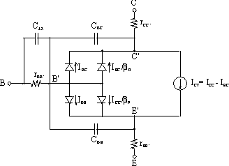
The starting point of this research to model high-power microwave BJTs is the standard Gummel-Poon model. Figure 1 depicts the basic circuit topology.
Figure 1. Topology of the basic Gummel-Poon model.
The relevant governing current equations for this circuit model are represented as follows:
![]()
|
(1) |
|
(2) |
|
(3) |
|
(4) |
![]()
The main reason for choosing the Gummel-Poon model as a basic starting point for the proposed research into high-power microwave BJTs is that it is a very well-understood, time-tested model, and it already has a set of static equations governing the electro-thermal behavior of the most temperature-sensitive parameters. These parameters include:
Thermal potential:
|
|
(5) |
|
|
(6) |
Intrinsic carrier concentration: |
|
(7) |
Transport saturation current |
|
(8) |
Forward beta: |
|
(9) |
Reverse beta: |
|
(10) |
Base-emitter leakage current: |
|
(11) |
|
|
(12) |
|
|
(13) |
|
|
(14) |
Based upon these relations, the next step in assessing self-heating effects is to develop a way of computing the junction temperature for the transistor. This can be done by starting with the energy balance equation
|
(15) |
where
|
is the energy entering the system (in our approach we assume no external heating and that the only thermal energy source in the system is the transistor itself). |
|
is the energy generated in the system (this energy is equal to the power dissipated by the device and is in general dependent on the spatial extent of the device). |
|
is the energy leaving the system, where K(T) is the thermal conductivity of the material. The thermal conductivity should take into account the presence of the casing and any heat-sinks. |
|
is the energy stored in the system, where r is the semiconductor material density and c is the specific heat constant. |
Substitution of these values into (15) results in the dynamic heat equation
|
(16) |
|
|
||
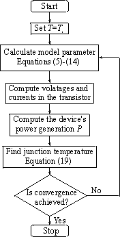
Figure 2. Block diagram of the algorithm. |
||

This is a three-dimensional nonlinear partial differential equation that can not be solved analytically; it requires a numerical solution. However, since in most cases the exact internal structure of the device is unknown, we cannot compute a 3D distribution of the power dissipation. For this reason we treat (16) as a lumped one-dimensional equation where the 1D model incorporates the actual 3D nature of the device in a similar way as a lumped circuit elements encode the true 3D spatial extent of the component. Once in 1D form, further simplifications can be made by employing the so-called Kirchoff transformation that allows us to transform (16) into a linear differential equation. The thermal conductivity of Si and GaAs can be approximated as K(T)=K(T0)(T/T0)n , where n = -1.25 for Si. This permits a conversion of equation (16) into
|
(17) |
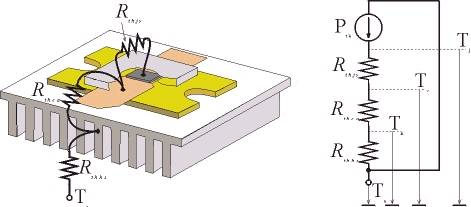
where the thermal resistance RTH is equal to K-1(T0) and the thermal capacitance is CTH=ρc. For the static case, equation (17) can be solved analytically with the solution of
|
(18) |
For the dynamic case equation (17) has to be evaluated numerically. In both cases the solution to (17) gives the average junction temperature in the transistor from the known dissipated power P. This allows us to readjust the model parameters dynamically by using equations (5) through (14). The required computation algorithm that summarizes the proposed approach is shown in Figure 2.
Measurements
This section describes a preliminary list of experiments that have to be conducted in order to extract and validate the proposed model. Due to the lack of equipment at WPI, all measurements need to be performed at M/A-Com facilities. In the initial phase of the project, when a model is developed and tested, it is helpful to have access to the on-wafer measurement, thus eliminating the need for taking into account all parasitics related to the transistor casing. The specific measurements that have to be performed include the following protocol:
Measure DC I-V characteristics and bias-dependent S-parameters.
Extract small-signal BJT model directly or through optimization using available approaches.
Extract large-signal model from DC and small-signal S-parameter data
Measure pulsed base or collector I-V characteristics to extract thermal capacitance CTH.
Measure base/collector current at different temperatures up to 150C and extract thermal impedance RTH of a BJT.
Extract static high-current effects using pulsed and DC measurements taking into account self-heating effect.
Using Microwave Transition Analyzer or a Fast Sampling Oscilloscope, measure the input and output waveforms of a BJT under different bias, match, and drive conditions. Based on the measured waveforms, perform model validation and adjustment of parameters to fit time-domain large-signal waveforms.
Use waveform measurements to assess RF breakdown versus DC breakdown characteristics of a BJT.
Repeat steps 1-7 for at least three BJTs of the same wafer and calculate the mean values and standard deviation of model parameters.
Validate the model by comparing the measured versus modeled DC I-V characteristics, small-signal S-parameters, and large-signal waveforms. In addition the model will be used to simulate Pout, harmonic power, PAE, gain, and Ic, Ib as a function of Pin.
Introduce any changes to the standard Gummel-Poon model that may be necessary to improve the model accuracy in terms of electrical and thermal performance.
Wyszukiwarka
Podobne podstrony:
High Fidelity Modeling of Computer Network Worms
Castles & Crusades Wilderlands of High Adventure
Modeling of Polymer Processing and Properties
Hydrodynamic Modeling Of Sailing Yachts(1)
Capability of high pressure cooling in the turning of surface hardened piston rods
Anatomy Based Modeling of the Human Musculature
(WinD Power) Dynamic Modeling of Ge 1 5 And 3 6 Wind Turbine Generator {}[2003}
Monitoring the Risk of High Frequency Returns on Foreign Exchange
Modeling Of The Wind Turbine With A Doubly Fed Induction Generator For Grid Integration Studies
W Borek Mechanical properties of high manganese austenitic TWIP type steel
Prediction Of High Weight Polymers Glass Transition Temperature Using Rbf Neural Networks Qsar Qspr
Comparison of theoretical and experimental free vibrations of high industrial chimney interacting
80 1125 1146 Spray Forming of High Alloyed Tool Steels to Billets of Medium Size Dimension
10 Grandes Etudes for Clarinet of High Virtuosity (clarinet) Fernand Carion
collimated flash test and in sun measurements of high concentration photovoltaic modules
Castles & Crusades Wilderlands of High Adventure
Modeling of Polymer Processing and Properties
Heinlein, Robert A The Good News of High Frontier
więcej podobnych podstron


