372596183
182 S. Takahashi et al.
at the location of AB1 for thermal load tests we did a beam dynamical analysis.
|
7 |
\ |
i | | ||
|
/ |
\ | |||
|
1 |
\ | |||
|
• - . |
\ | |||
|
• 1 1 1 1 • • 1 |
! • i | i .i .i-i |
• i /■« / .. |
i— - i - i i i
0 12)4
Beam Radiu* (mm)
Fig. 3. Beam current profile obtained from a beam
orbital analysis.
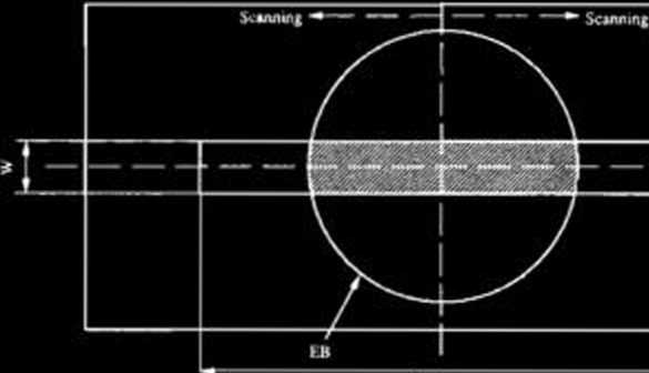
A typical beam current profile obtained from the analysis is shown in Fig. 3, which shows that the beam diameter at the location of AB is 6.4 mm. This value is larger than that expected because of a Iow accelerating voltage. To carry out an experiment similar to a practical SR, the scanning width of E.B. is to be reduced to below 1 mm with a slit madę of tungsten, as shown in Fig. 4. We have to increase the current of E.B. to the value at which a beam power passing through the slit (the slashed area in Fig. 4) is 1.2 kW. Therefore, if we utilize the slit of W =0.1 cm, the power density for 18 mm scanning is 6.7 kW / cm2. For the same power density (~26.7 kW/cm2) as the practical one, W =0.025 cm is required. Problems are whether such a smali slit width can be machined accurately, and whether the total power of a beam passing through the slit of W =0.025 cm can be 1.2 kW with this E.B. Gun (Maximum total power = 5 kW). Therefore, for the time being, our experi-ments are focused on the investigation of the inside conditions of cooling channels and the temperaturę gradient on the absorber by using a slit of W = 0.1 cm. A thermal analysis under actual experimental conditions will be perform-ed in parallel with the experiments.
łv ■-Sin

llfiwn
Fig. 4. Relation between E.B. and a slit width.
References
1) Y. Morimoto, S. Yokouchi, H. Sakamoto, S.H. Be, and T. Shirakura: RIKEN Accel. Próg. Rep., 22, 292 (1988).
2) Y. Morimoto, T. Shirakura, K. Konishi, and S.H. Be: This Report, p. 183.
Wyszukiwarka
Podobne podstrony:
118 T. Wilgat et al. Although the amount of circulating water is smali, there are nunerous lakes — n
144 T. Wilgat et al. distinguished. The beginning of the first goes back into prehistorical time, an
- 3 - i {As Buffalo at the ena of Maj - for "pretsure on Washington to sup ort tne Polish exil
282 Z. KORUBA ET AL. yv - yertical displacement of the turret mass centre Sv, (fv - angle of rotatio
18 M. Sajewicz et al. Basic qualitative features of the composition of the volatile fractions origir
174 Piotr Górski et al. Wojterski (eds). Atlas of the geographical distri-bution of spore plants in
image003 Hesgotone extraordinary chance at the dream of a lifetimę. Alex Rogan is a small-
koliber II (25) Stóney Creek Collection, Inc.. (D2005 MMM & a m & aj SPECIAL NOTĘ: The blue
m1447
ss 025 A PHYSIQUE TO BE PROUD OF—SHOWS YOU WHAT TO EXPECT AT THE END OF THE SIX MONTHS COURSE Posiał
20 usually take place at the begirming of summer and at the beginning of winter. Periodical seininom
więcej podobnych podstron