456719260

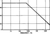
Figurę 4a. CMRR Over Freguency

DIGITAL CURRENTS SHARE CONDUCTOR
Table I. AD670 Input Selecdon/Output Format Truth Table
|
BPO/UPO |
FORMAT |
INPUT RANGĘ/ OUTPUT FORMAT |
|
0 |
0 |
Unipolar/Straight Binary |
|
1 |
0 |
Bipolar/Offset Binary |
|
0 |
1 |
Unipolar/2s Complement |
|
1 |
1 |
Bipolar/2s Complement |
DIFF
STRAIGHT BINARY_
(FORMAT = 0, BPO/UPO = 0) 0000 0000 1000 0000 1111 1111 0000 0000 0000 0001 11111111
-V|N
V|N
128 mV 255 mV 0
1 mV 255 mV
255 mV 127 mV -127 mV
Figurę 4b. AD670 Input Rejects Common-Mode Ground Noise
Good common-mode performance is useful in a number of situ-ations. In bridge-type transducer applications, such performance facilitates the recovery of differential analog signals in the pres-ence of a dc common-mode or a noisy electrical environment. High freąuency CMRR also becomes important when the analog signal is referred to a noisy, remote digital ground. In each case, the CMRR specification of the AD670 allows the integrity of the input signal to be preserved.
The AD670’s common-mode voltage tolerance allows great flexibility in Circuit layout. Most other A/D converters require the establishment of one point as the analog reference point. This is necessary in order to minimize the effects of parasitic voltages. The AD670, however, eliminates the need to make the analog ground reference point and A/D analog ground one and the same. Instead, a system such as that shown in Figurę 4b is possible as a result of the AD670’s common-mode performance. The resistors and inductors in the ground return represent un-avoidable system parasitic impedances.
Input/Output Options
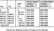
Data output coding (2s complement vs. straight binary) is selected using Pin 12, the FORMAT pin. The selection of input format (bipolar vs. unipolar) is controlled using Pin 11, BPO/UPO. Prior to a write/convert, the State of FORMAT and BPO/UPO should be available to the converter. These lines may be tied to the data bus and may be changed with each conver-sion if desired. The configurations are shown in Table I. Output coding for representative signals in each of these configurations is shown in Figurę 5.
An output signal, STATUS, indicates the status of the conver-sion. STATUS goes high at the beginning of the conversion and retums Iow when the conversion cycle has been completed.
+V|N
0
128 mV 255 mV 255 mV 128 mV 128 mV
Figurę 5a. Unipolar Output Codes (Low Rangę)

Calibration
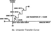
Because of its precise factory calibration, the AD670 is intended to be operated without user trims for gun and offset; therefore, no provisions have been madę for such user trims. Figures 6a, 6b, and 6c show the transfer curves at zero and fuli scalę for the unipolar and bipolar modes. The codę transitions are positioned so that the desired value is centered at that codę. The first LSB transition for the unipolar modę occurs for an input of +1/2 LSB (5 mV or 0.5 mV). Similarly, the MSB transition for the bipolar modę is set at -1/2 LSB (-5 mV or -0.5 mV). The fuli scalę transition is located at the fuli scalę value -1 1/2 LSB. These values are 2.545 V and 254.5 mV.

Wyszukiwarka
Podobne podstrony:
kg fig4a Figurę 4a
policjaOVouTube°L #BanCash #Dystopia #BigBrotherGovernment Digital Currency: Why You Should Be
Figurę 1.15. Global imbalances remain elevated Current account balance, in per cent of world GDP 199
New test methods for MIMO OTA measurements Currently, OTA performance tests for single input si
AD670 INPUT CONNECTIONS Standard connections are shown in the figures that follow. An input rangę of
63 Figurę 2.3 Mass and sex independent Msum variation over the natural rangę of weather conditions.
Figurę 8: Non-LCC Premium Over LCC Price on Similar-Distance Routes 2000s, reflecting their lower bu
Figurę 4: Implied Changes In Domestic Airline Demand Over Time years. Yet, the industry madę money i
Figurę 6: Domestic Market Share of Low-Cost Carriers from this figurę. First, LCCs in aggregate have
2SC1674 POWER GAIN, NOISE FIGURĘ NF* Noise Figurę -dB Ig — Emitter Current— mA
Digital marketing: evoluzk>ni e nuove figurę professionali Master in Marketing Managerrent
więcej podobnych podstron