5441337091
!«('.j)=f(M)+k■-«»(■*.>) A **
U(U)= /(*./) M»<h
where/i, j) is the image without enhancement, g(i, j) is the image with enhancement, and A is a weight.
This algorithm can enhance the images by increasing the grayscale of the solder pastę part, so the solder pastę and the base of PCB can be distinguished easily. The enhanced images can be separated into pad particie, solder pastę particie and dark loop around solder pastę particie by using a multi-thresholds fimction.
V. INSPKTION METHOD
A. 2D Inspection Based on Particie Analyze method
The Particie analysis method has many advantages, such as simple and high speed. Furthermore, many particie factors are shift, scaling and rotation invariant. Thus, the particie analysis approach is suitable for 2D inspection.
The defects of solder pastę depositing can be inspected by analyzing the position, area and shape of the particles of solder pastę and pads, which can be expressed by the following factors [8],
Center: center position of the particie.
A: area of the particie.
Ak: area of the hole in the particie.
Ach-. Area of the particie Convex Hull.
P: Length of the outer boundary of the particie.
Hydraulic Radius: The particie area divided by the particie perimeter.
Heywood Circularity Factor: HC=P/(2sqrt( n A)),
Perimeter divided by the circumference of a circle with the same area. The closer the shape of the particie is to a disk, the closer the Heywood circularity factor is to 1.
moment of inertia with respect to the* axis.
lyy. moment of inertia with respect to the y axis.
Type Factor: TF = A2 !(\n sqrt(l„ ■!„)), the type of the particie.
Packing Ratio: PR= A/(A + Ak) , it is used to judge whether deficiency of solder pastę exist or not.
The values of the factor mentioned above are inputted to the defect analyzer after being calculated. The defect analyzer is used to determine the defect existing or not by using a synthesis weight method. The defect analyzer can find out the defects of the solder pastę, such as displacement, deficiency, excess, bridge and overflow. Though the 2D inspection method can determine most of the solder pastę depositing defects, it can not inspect the volume defects of solder pastę deposition.
B. Pseudo-3D inspection
Notę that the 3D inspection algorithm can find out the defects of pastę dose in volume, however, it needs a laser scanner and it is relatively slowly. To overcome these disadvantages, a pseudo-3D inspection approach was used in order to calculate the volume ratio by creating a simple 3D model of the solder pastę depositing.
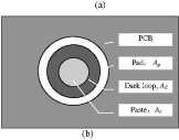
As shown in Fig. 3 (b), there is a dark loop around the solder pastę. One reason for the dark loop is that the PCB is illuminated by the coaxial illuminator of the vision system, thus the ray is perpendicular to the PCB according to the principle of reflecłion. If only the ray is perpendicular to the surface, the reflected ray is captured by the camera, so the image is bright; otherwise the image is dark, as shown in Fig. 4(a).


figurę 4. 3D Model of Solder pasie. The (a) is Ihe ade view and the (b) is
As shown in Fig. 4(b), Ap is the area of particie of the pad, Ajis the area of particie of the solder pastę and Ad is the area of particie of the dark loop around the solder pastę. The volume ratio of the solder pastę deposit can be obtained by
Va IV, =1/2(A, +(A, + Ad)h/(Ap A)= (1/2Ą, + A,)/Ap
(2)
where Va represents the actual volume of the solda pastę and V, is the theoretical volume of the solda pastę.
The defects can be found out by a threshold according to the volume ratio. This pseudo-3D inspection method can be carried out fast compare with the łasa scanna inspection.
VI. EXPERIMENT AND ANALYSIS
In order to verify the performance of the integrated method, some expaiments have been carried out. The machinę vision system was shown in Fig. 5, the vision system includes a NI-PCI1409 image acquire card, two Teli-Cs8630i camaas, two AllyVision-COR30 coaxial illuminators. The solder pastę is lead iree.
Wyszukiwarka
Podobne podstrony:
00065 ndb3dfcfa3fd16c12bb4b6de5950d85 64 Hembree & Zimmer X where Y, is the entire data sample
18b Odpowiedź: c)
Hail Mary in the Bible http:/. netny.net. resouiccs mary bible-htmlQ: Where is the Hail Mary in the
CCF20100310�007 approximate form is: S(t) = F + A sin[<j)0 + fc(v0r + x/igt2)]
Plansze?ukacyjne H Odpowiedź: c)
IV. ZDANIA MIESZANE4. Przekształć pytania bezpośrednie na pośrednie. 1.
img117 (18) l/i OŻ0C9 59. A: Would you like to try this jacket on? B: I think J wi
str0052 jpeg 2 •• ■‘30 Listen to the song and answer these ąuesdons. Where is the
str0052 2 •• ■‘30 Listen to the song and answer these ąuesdons. Where is the singe
Where is the Substrate in the Germanie Lexicon?ROLAND SCHUHMANN Ntun di Science kctwccn both appłoae
Light previeui Ił is the image which •:hangę*I the LED lighting pattern. Plea e • h*" •• the o
Lesson3 p148 149 148_CONYERSATIONAL PORTUGUESE Onde ć o correio? Where is the post office? Na esąu
18b 2 Odpowiedź: c)172Odpowiedź: a)171 Where is the nearest filling station? nearest najbliższy next
więcej podobnych podstron