1
Features
•
High-performance, Low-power AVR
®
8-bit Microcontroller
•
Advanced RISC Architecture
– 90 Powerful Instructions – Most Single Clock Cycle Execution
– 32 x 8 General Purpose Working Registers
– Fully Static Operation
•
Non-volatile Program and Data Memories
– 1K Byte In-System Programmable Flash Program Memory
Endurance: 1,000 Write/Erase Cycles
– 64 Bytes EEPROM
Endurance: 100,000 Write/Erase Cycles
– Programming Lock for Flash Program Data Security
•
Peripheral Features
– Interrupt and Wake-up on Pin Change
– Two 8-bit Timer/Counters with Separate Prescalers
– One 150 kHz, 8-bit High-speed PWM Output
– 4-channel 10-bit ADC
One Differential Voltage Input with Optional Gain of 20x
– On-chip Analog Comparator
– Programmable Watchdog Timer with On-chip Oscillator
•
Special Microcontroller Features
– In-System Programmable via SPI Port
– Enhanced Power-on Reset Circuit
– Programmable Brown-out Detection Circuit
– Internal, Calibrated 1.6 MHz Tunable Oscillator
– Internal 25.6 MHz Clock Generator for Timer/Counter
– External and Internal Interrupt Sources
– Low-power Idle and Power-down Modes
•
Power Consumption at 1.6 MHz, 3V, 25
°C
– Active: 3.0 mA
– Idle Mode: 1.0 mA
– Power-down: < 1 µA
•
I/O and Packages
– 8-lead PDIP and 8-lead SOIC: 6 Programmable I/O Lines
•
Operating Voltages
– 2.7V - 5.5V
•
Internal 1.6 MHz System Clock
Pin Configuration
1
2
3
4
8
7
6
5
(RESET/ADC0) PB5
(ADC3) PB4
(ADC2) PB3
GND
VCC
PB2 (ADC1/SCK/T0/INT0)
PB1 (AIN1/MISO/OC1A)
PB0 (AIN0/AREF/MOSI)
PDIP/SOIC
8-bit
Microcontroller
with 1K Byte
Flash
ATtiny15L
Rev. 1187F–AVR–06/05

2
ATtiny15L
1187F–AVR–06/05
Description
The ATtiny15L is a low-power CMOS 8-bit microcontroller based on the AVR RISC
architecture. By executing powerful instructions in a single clock cycle, the ATtiny15L
achieves throughputs approaching 1 MIPS per MHz allowing the system designer to
optimize power consumption versus processing speed.
The AVR core combines a rich instruction set with 32 general purpose working registers.
All the 32 registers are directly connected to the Arithmetic Logic Unit (ALU), allowing
two independent registers to be accessed in one single instruction executed in one clock
cycle. The resulting architecture is more code efficient while achieving throughputs up to
ten times faster than conventional CISC microcontrollers.
The ATtiny15L provides 1K byte of Flash, 64 bytes EEPROM, six general purpose I/O
lines, 32 general purpose working registers, two 8-bit Timer/Counters, one with high-
speed PWM output, internal Oscillators, internal and external interrupts, programmable
Watchdog Timer, 4-channel 10-bit Analog-to-Digital Converter with one differential volt-
age input with optional 20x gain, and three software-selectable Power-saving modes.
The Idle mode stops the CPU while allowing the ADC, anAlog Comparator,
Timer/Counters and interrupt system to continue functioning. The ADC Noise Reduction
mode facilitates high-accuracy ADC measurements by stopping the CPU while allowing
the ADC to continue functioning. The Power-down mode saves the register contents but
freezes the Oscillators, disabling all other chip functions until the next interrupt or Hard-
ware Reset. The wake-up or interrupt on pin change features enable the ATtiny15L to
be highly responsive to external events, still featuring the lowest power consumption
while in the Power-saving modes.
The device is manufactured using Atmel’s high-density, Non-volatile memory technol-
ogy. By combining a RISC 8-bit CPU with Flash on a monolithic chip, the ATtiny15L is a
powerful microcontroller that provides a highly flexible and cost-efficient solution to
many embedded control applications. The peripheral features make the ATtiny15L par-
ticularly suited for battery chargers, lighting ballasts and all kinds of intelligent sensor
applications.
The ATtiny15L AVR is supported with a full suite of program and system development
tools including macro assemblers, program debugger/simulators, In-circuit emulators
and evaluation kits.
3
ATtiny15L
1187F–AVR–06/05
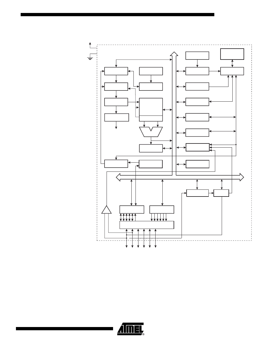
Block Diagram
Figure 1. The ATtiny15L Block Diagram
PROGRAM
COUNTER
INTERNAL
OSCILLATOR
WATCHDOG
TIMER
STACK
POINTER
PROGRAM
FLASH
HARDWARE
STACK
MCU CONTROL
REGISTER
GENERAL
PURPOSE
REGISTERS
INSTRUCTION
REGISTER
TIMER/
COUNTER0
INSTRUCTION
DECODER
DATA DIR.
REG.PORT B
DATA REGISTER
PORT B
PROGRAMMING
LOGIC
TIMING AND
CONTROL
TIMER/
COUNTER1
MCU STATUS
REGISTER
STATUS
REGISTER
ALU
PORT B DRIVERS
PB0-PB5
VCC
GND
CONTROL
LINES
+
-
ANALOG
COMPARATOR
8-BIT DATA BUS
Z
ISP MODULE
INTERRUPT
UNIT
DATA
EEPROM
INTERNAL
OSCILLATOR
TUNABLE
ANALOG MUX
ADC

4
ATtiny15L
1187F–AVR–06/05
Pin Descriptions
VCC
Supply voltage pin.
GND
Ground pin.
Port B (PB5..PB0)
Port B is a 6-bit I/O port. PB4..0 are I/O pins that can provide internal pull-ups (selected
for each bit). PB5 is input or open-drain output. The use of pin PB5 is defined by a fuse
and the special function associated with this pin is External Reset. The port pins are tri-
stated when a reset condition becomes active, even if the clock is not running.
Port B also accommodates analog I/O pins. The Port B pins with alternate functions are
shown in Table 1.
Analog Pins
Up to four analog inputs can be selected as inputs to Analog-to-Digital Converter (ADC).
Internal Oscillators
The internal Oscillator provides a clock rate of nominally 1.6 MHz for the system clock
(CK). Due to large initial variation (0.8 -1.6 MHz) of the internal Oscillator, a tuning capa-
bility is built in. Through an 8-bit control register – OSCCAL – the system clock rate can
be tuned with less than 1% steps of the nominal clock.
There is an internal PLL that provides a 16x clock rate locked to the system clock (CK)
for the use of the Peripheral Timer/Counter1. The nominal frequency of this peripheral
clock, PCK, is 25.6 MHz.
Table 1. Port B Alternate Functions
Port Pin
Alternate Function
PB0
MOSI (Data Input Line for Memory Downloading)
AREF (ADC Voltage Reference)
AIN0 (Analog Comparator Positive Input)
PB1
MISO (Data Output Line for Memory Downloading)
OC1A (Timer/Counter PWM Output)
AIN1 (Analog Comparator Negative Input)
PB2
SCK (Serial Clock Input for Serial Programming)
INT0 (External Interrupt0 Input)
ADC1 (ADC Input Channel 1)
T0 (Timer/Counter0 External Counter Input)
PB3
ADC2 (ADC Input Channel 2)
PB4
ADC3 (ADC Input Channel 3)
PB5
RESET (External Reset Pin)
ADC0 (ADC Input Channel 0)
5
ATtiny15L
1187F–AVR–06/05
ATtiny15L
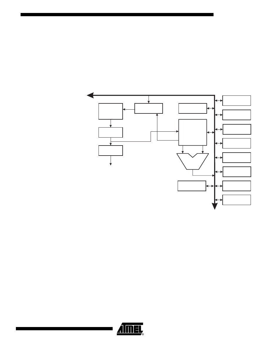
Architectural
Overview
The fast-access Register File concept contains 32 x 8-bit general purpose working reg-
isters with a single-clock-cycle access time. This means that during one single clock
cycle, one ALU (Arithmetic Logic Unit) operation is executed. Two operands are output
from the Register File, the operation is executed, and the result is stored back in the
Register File – in one clock cycle.
Two of the 32 registers can be used as a 16-bit pointer for indirect memory access. This
pointer is called the Z-pointer, and can address the Register File, IO file and the Flash
Program memory.
Figure 2. The ATtiny15L AVR RISC Architecture
The ALU supports arithmetic and logic functions between registers or between a con-
stant and a register. Single-register operations are also executed in the ALU. Figure 2
shows the ATtiny15L AVR RISC microcontroller architecture. The AVR uses a Harvard
architecture concept with separate memories and buses for program and data memo-
ries. The program memory is accessed with a two-stage pipeline. While one instruction
is being executed, the next instruction is pre-fetched from the program memory. This
concept enables instructions to be executed in every clock cycle. The Program memory
is In-System Programmable Flash memory.
With the relative jump and relative call instructions, the whole address space is directly
accessed. All AVR instructions have a single 16-bit word format, meaning that every
program memory address contains a single 16-bit instruction.
During interrupts and subroutine calls, the return address Program Counter (PC) is
stored on the Stack. The Stack is a 3-level-deep Hardware Stack dedicated for subrou-
tines and interrupts.
The I/O memory space contains 64 addresses for CPU peripheral functions as Control
Registers, Timer/Counters and other I/O functions. The memory spaces in the AVR
architecture are all linear and regular memory maps.
512 x 16
Program
FLASH
Instruction
Register
Instruction
Decoder
Program
Counter
Control Lines
32 x 8
General
Purpose
Registrers
ALU
Direct Addressing
Status
and Test
Control
Registrers
Interrupt
Unit
2 x 8-bit
Timer/Counter
Watchdog
Timer
Analog
Comparator
I/O Lines
Data Bus 8-bit
SPI Unit
ADC
64 x 8
EEPROM

6
ATtiny15L
1187F–AVR–06/05
A flexible interrupt module has its control registers in the I/O space with an additional
Global Interrupt Enable bit in the Status Register. All the different interrupts have a sep-
arate Interrupt Vector in the Interrupt Vector table at the beginning of the program
memory. The different interrupts have priority in accordance with their Interrupt Vector
position. The lower the Interrupt Vector address, the higher the priority.
The General Purpose
Register File
Figure 3 shows the structure of the 32 general purpose registers in the CPU.
Figure 3. AVR CPU General Purpose Working Registers
All the register operating instructions in the instruction set have direct- and single-cycle
access to all registers. The only exception is the five constant arithmetic and logic
instructions SBCI, SUBI, CPI, ANDI, and ORI between a constant and a register and the
LDI instruction for load-immediate constant data. These instructions apply to the second
half of the registers in the Register File – R16..R31. The general SBC, SUB, CP, AND,
OR, and all other operations between two registers or on a single-register apply to the
entire Register File.
Registers 30 and 31 form a 16-bit pointer (the Z-pointer) which is used for indirect Flash
memory and Register File access. When the Register File is accessed, the contents of
R31 is discarded by the CPU.
The ALU – Arithmetic
Logic Unit
The high-performance AVR ALU operates in direct connection with all the 32 general
purpose working registers. Within a single clock cycle, ALU operations between regis-
ters in the Register File are executed. The ALU operations are divided into three main
categories – arithmetic, logic and bit-functions. Some microcontrollers in the AVR prod-
uct family feature a hardware multiplier in the arithmetic part of the ALU.
The Flash Program
Memory
The ATtiny15L contains 1K byte On-chip, In-System Programmable Flash memory for
program storage. Since all instructions are single 16-bit words, the Flash is organized as
512 x 16 words. The Flash memory has an endurance of at least 1,000 write/erase
cycles.
The ATtiny15L Program Counter is nine bits wide, thus addressing the 512 words Flash
Program memory.
See page 54 for a detailed description on Flash memory programming.
7
0
R0
R1
R2
General
…
Purpose
…
Working
R28
Registers
R29
R30 (Z-register Low Byte)
R3
R31 (Z-register High Byte)
7
ATtiny15L
1187F–AVR–06/05
The Program and Data
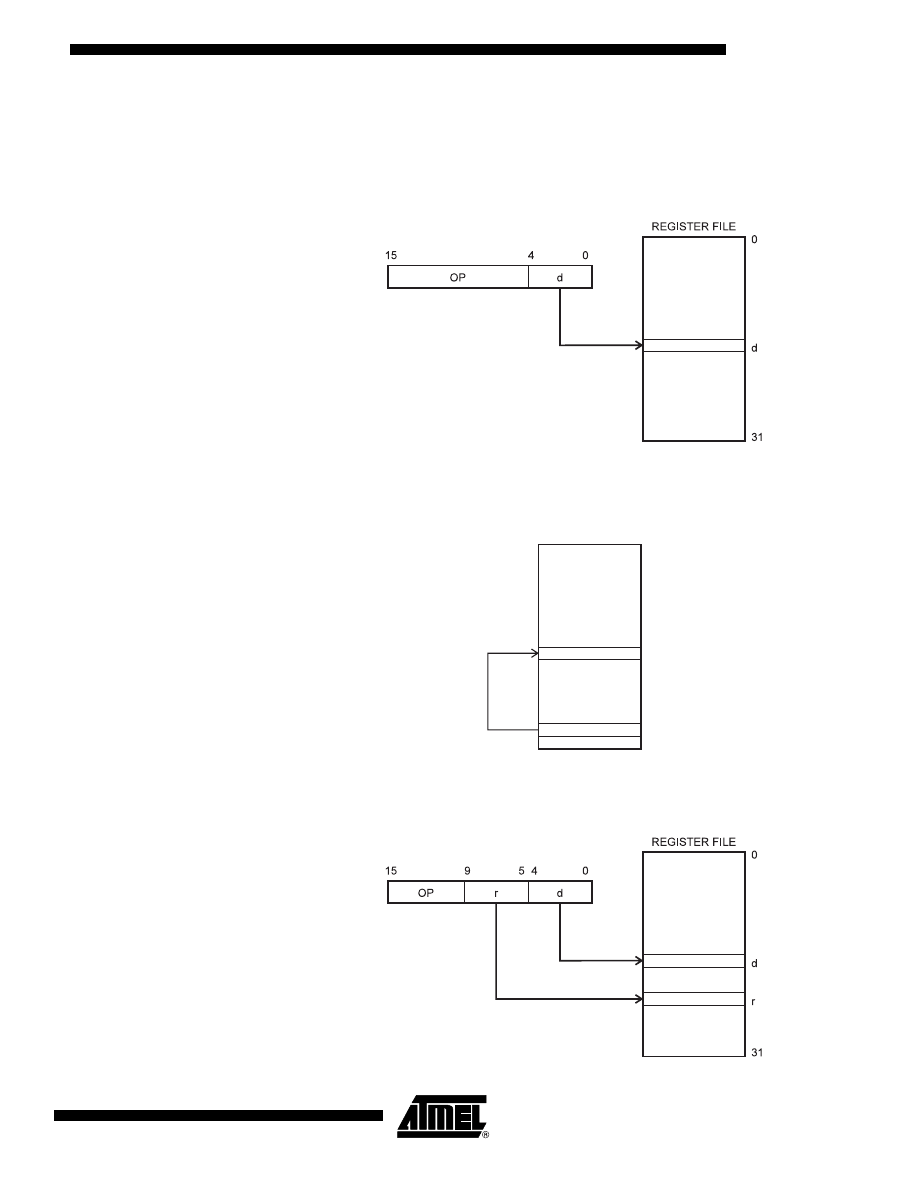
Addressing Modes
The ATtiny15L AVR RISC Microcontroller supports powerful and efficient addressing
modes. This section describes the various addressing modes supported in the
ATtiny15L. In the figures, OP means the operation code part of the instruction word. To
simplify, not all figures show the exact location of the addressing bits.
Register Direct, Single-
register Rd
Figure 4. Direct Single-register Addressing
The operand is contained in register d (Rd).
Register Indirect
Figure 5. Indirect Register Addressing
The register accessed is the one pointed to by the Z-register low byte (R30).
Register Direct, Two Registers
Rd and Rr
Figure 6. Direct Register Addressing, Two Registers
REGISTER FILE
0
31
30
Z-register
8
ATtiny15L
1187F–AVR–06/05
Operands are contained in register r (Rr) and d (Rd). The result is stored in register d
(Rd).
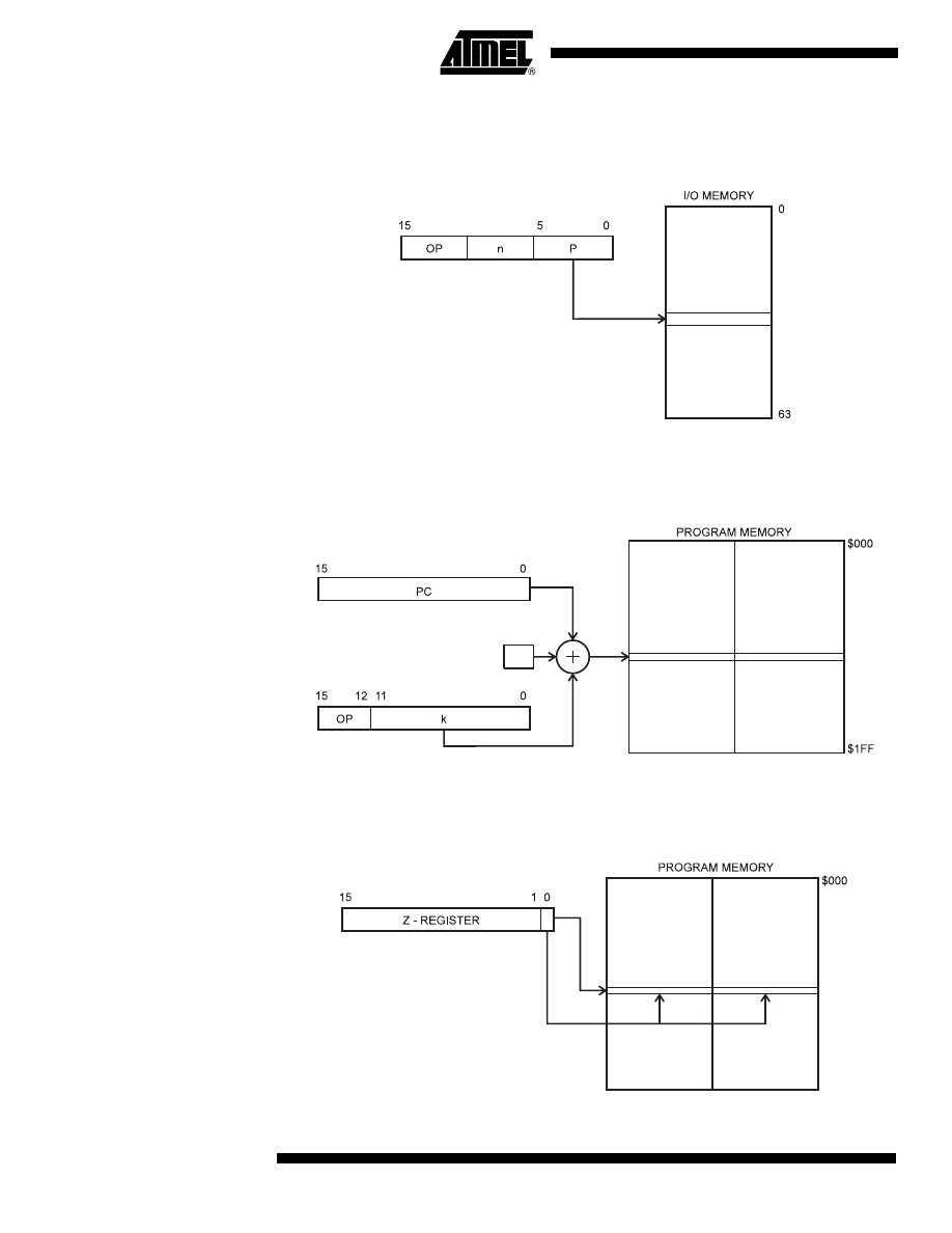
I/O Direct
Figure 7. I/O Direct Addressing
Operand address is contained in 6 bits of the instruction word. “n” is the destination or
source register address.
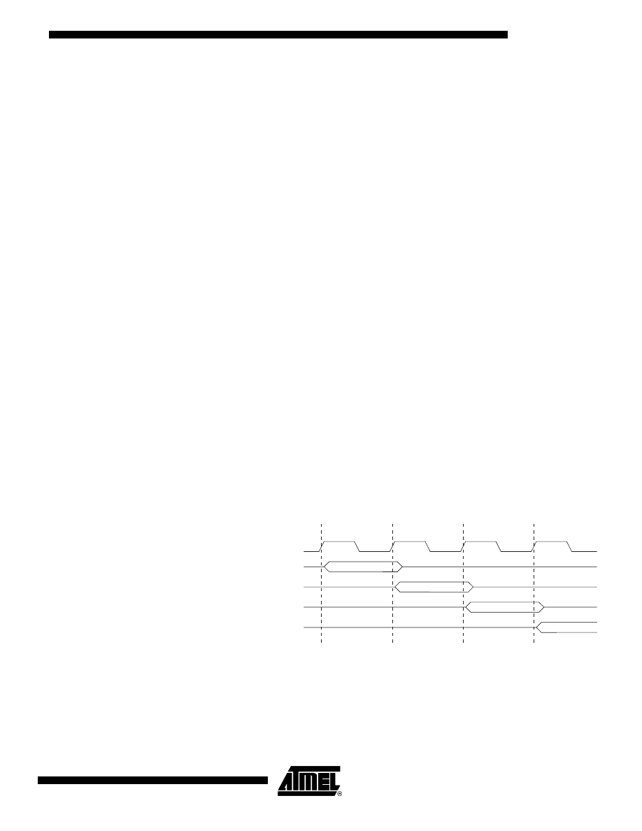
Relative Program Addressing,
RJMP and RCALL
Figure 8. Relative Program Memory Addressing
Program execution continues at address PC + k + 1. The relative address k is -2048 to
2047.
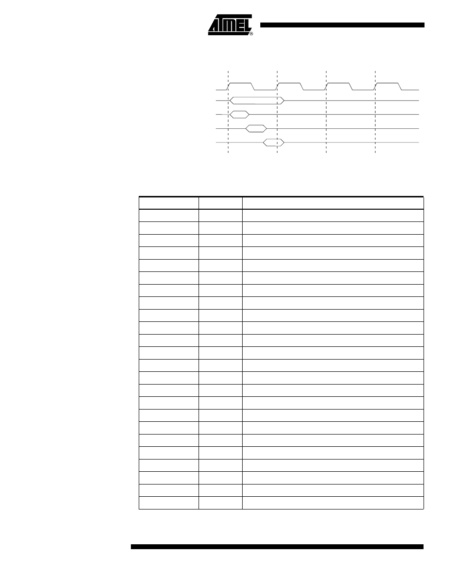
Constant Addressing using
the LPM Instruction
Figure 9. Code Memory Constant Addressing
+1
$1FF
9
ATtiny15L
1187F–AVR–06/05
Constant byte address is specified by the Z-register contents. The 15 MSBs select word
address (0 - 511), and LSB selects low byte if cleared (LSB = 0) or high byte if set
(LSB = 1).
Subroutine and Interrupt
Hardware Stack
The ATtiny15L uses a 3-level-deep Hardware Stack for subroutines and interrupts. The
Hardware Stack is nine bits wide and stores the Program Counter (PC) return address
while subroutines and interrupts are executed.
RCALL instructions and interrupts push the PC return address onto Stack level 0, and
the data in the other Stack levels 1 - 2 are pushed one level deeper in the Stack. When
a RET or RETI instruction is executed the returning PC is fetched from Stack level 0,
and the data in the other Stack levels 1 - 2 are popped one level in the Stack.
If more than three subsequent subroutine calls or interrupts are executed, the first val-
ues written to the Stack are overwritten. Pushing four return addresses A1, A2, A3, and
A4 followed by four subroutine or interrupt returns, will pop A4, A3, A2, and once more
A2 from the Hardware Stack.
The EEPROM Data
Memory
The ATtiny15L contains 64 bytes of data EEPROM memory. It is organized as a sepa-
rate data space, in which single bytes can be read and written. The EEPROM has an
endurance of at least 100,000 write/erase cycles. The access between the EEPROM
and the CPU is described on page 36, specifying the EEPROM Address Register, the
EEPROM Data Register, and the EEPROM Control Register.
Memory Access and
Instruction Execution Timing
This section describes the general access timing concepts for instruction execution and
internal memory access.
The AVR CPU is driven by the System Clock Ø, directly generated from the external
clock crystal for the chip. No internal clock division is used.
Figure 10 shows the parallel instruction fetches and instruction executions enabled by
the Harvard architecture and the fast-access Register File concept. This is the basic
pipelining concept to obtain up to 1 MIPS per MHz with the corresponding unique results
for functions per cost, functions per clocks, and functions per power-unit.
Figure 10. The Parallel Instruction Fetches and Instruction Executions
Figure 11 shows the internal timing concept for the Register File. In a single clock cycle
an ALU operation using two register operands is executed, and the result is stored back
to the destination register.
System Clock Ø
1st Instruction Fetch
1st Instruction Execute
2nd Instruction Fetch
2nd Instruction Execute
3rd Instruction Fetch
3rd Instruction Execute
4th Instruction Fetch
T1
T2
T3
T4
10
ATtiny15L
1187F–AVR–06/05
Figure 11. Single Cycle ALU Operation
I/O Memory
The I/O space definition of the ATtiny15L is shown in Table 2.
System Clock Ø
Total Execution Time
Register Operands Fetch
ALU Operation Execute
Result Write Back
T1
T2
T3
T4
Table 2. ATtiny15L I/O Space
Address Hex
Name
Function
$3F
SREG
Status Register
$3B
GIMSK
General Interrupt Mask Register
$3A
GIFR
General Interrupt Flag Register
$39
TIMSK
Timer/Counter Interrupt Mask Register
$38
TIFR
Timer/Counter Interrupt Flag Register
$35
MCUCR
MCU Control Register
$34
MCUSR
MCU Status Register
$33
TCCR0
Timer/Counter0 Control Register
$32
TCNT0
Timer/Counter0 (8-bit)
$31
OSCCAL
Oscillator Calibration Register
$30
TCCR1
Timer/Counter1 Control Register
$2F
TCNT1
Timer/Counter1 (8-bit)
$2E
OCR1A
Timer/Counter1 Output Compare Register A
$2D
OCR1B
Timer/Counter1 Output Compare Register B
$2C
SFIOR
Special Function I/O Register
$21
WDTCR
Watchdog Timer Control Register
$1E
EEAR
EEPROM Address Register
$1D
EEDR
EEPROM Data Register
$1C
EECR
EEPROM Control Register
$18
PORTB
Data Register, Port B
$17
DDRB
Data Direction Register, Port B
$16
PINB
Input Pins, Port B
$08
ACSR
Analog Comparator Control and Status Register
$07
ADMUX
ADC Multiplexer Select Register

11
ATtiny15L
1187F–AVR–06/05
Note:
1. Reserved and unused locations are not shown in the table.
All ATtiny15L I/O and peripheral registers are placed in the I/O space. The I/O locations
are accessed by the IN and OUT instructions transferring data between the 32 general
purpose working registers and the I/O space. I/O Registers within the address range
$00 - $1F are directly bit-accessible using the SBI and CBI instructions. In these regis-
ters, the value of single bits can be checked by using the SBIS and SBIC instructions.
Refer to the instruction set chapter for more details. For compatibility with future
devices, reserved bits should be written zero if accessed. Reserved I/O memory
addresses should never be written.
The I/O and Peripheral Control Registers are explained in the following sections.
The Status Register – SREG
The AVR Status Register – SREG – at I/O space location $3F is defined as:
• Bit 7 – I: Global Interrupt Enable
The Global Interrupt Enable bit must be set (one) for the interrupts to be enabled. The
individual interrupt enable control is then performed in the Interrupt Mask Registers –
GIMSK and TIMSK. If the Global Interrupt Enable Register is cleared (zero), none of the
interrupts are enabled independent of the GIMSK and TIMSK values. The I-bit is cleared
by hardware after an interrupt has occurred, and is set by the RETI instruction to enable
subsequent interrupts.
• Bit 6 – T: Bit Copy Storage
The Bit Copy instructions BLD (Bit LoaD) and BST (Bit STore) use the T-bit as source
and destination for the operated bit. A bit from a register in the Register File can be cop-
ied into T by the BST instruction, and a bit in T can be copied into a bit in a register in the
Register File by the BLD instruction.
• Bit 5 – H: Half-carry Flag
The Half-carry Flag H indicates a half-carry in some arithmetic operations. See the
Instruction Set description for detailed information.
• Bit 4 – S: Sign Bit, S = N
⊕ V
The S-bit is always an exclusive or between the Negative Flag N and the Two’s Comple-
ment Overflow Flag V. See the Instruction Set description for detailed information.
• Bit 3 – V: Two’s Complement Overflow Flag
The Two’s Complement Overflow Flag V supports two’s complement arithmetics. See
the Instruction Set description for detailed information.
$06
ADCSR
ADC Control and Status Register
$05
ADCH
ADC Data Register High
$04
ADCL
ADC Data Register Low
Table 2. ATtiny15L I/O Space
(1)
(Continued)
Address Hex
Name
Function
Bit
7
6
5
4
3
2
1
0
$3F
I
T
H
S
V
N
Z
C
SREG
Read/Write
R/W
R/W
R/W
R/W
R/W
R/W
R/W
R/W
Initial Value
0
0
0
0
0
0
0
0

12
ATtiny15L
1187F–AVR–06/05
• Bit 2 – N: Negative Flag
The Negative Flag N indicates a negative result after the different arithmetic and logic
operations. See the Instruction Set description for detailed information.
• Bit 1 – Z: Zero Flag
The Zero Flag Z indicates a zero result after the different arithmetic and logic opera-
tions. See the Instruction Set description for detailed information.
• Bit 0 – C: Carry Flag
The Carry Flag C indicates a carry in an arithmetic or logic operation. See the Instruction
Set description for detailed information.
Reset and Interrupt
Handling
The ATtiny15L provides eight interrupt sources. These interrupts and the separate
Reset Vector each have a separate Program Vector in the Program memory space. All
the interrupts are assigned individual enable bits that must be set (one) together with the
I-bit in the Status Register in order to enable the interrupt.
The lowest addresses in the Program memory space are automatically defined as the
Reset and Interrupt Vectors. The complete list of vectors is shown in Table 3. The list
also determines the priority levels of the different interrupts. The lower the address the
higher is the priority level. RESET has the highest priority, and next is INT0 (the External
Interrupt Request 0), etc.
Table 3. Reset and Interrupt Vectors
Vector No.
Program Address
Source
Interrupt Definition
1
$000
RESET
External Reset, Power-on Reset,
Brown-out Reset, and Watchdog
Reset
2
$001
INT0
External Interrupt Request 0
3
$002
I/O Pins
Pin Change Interrupt
4
$003
TIMER1, COMPA
Timer/Counter1 Compare Match A
5
$004
TIMER1, OVF
Timer/Counter1 Overflow
6
$005
TIMER0, OVF
Timer/Counter0 Overflow
7
$006
EE_RDY
EEPROM Ready
8
$007
ANA_COMP
Analog Comparator
9
$008
ADC
ADC Conversion Complete

13
ATtiny15L
1187F–AVR–06/05
The most typical and general program setup for the Reset and Interrupt Vector
Addresses are:
Address
Labels
Code
Comments
$000
rjmp
RESET
; Reset handler
$001
rjmp
EXT_INT0
; IRQ0 handler
$002
rjmp
PIN_CHANGE
; Pin change handler
$003
rjmp
TIM1_CMP
; Timer1 compare match
$004
rjmp
TIM1_OVF
; Timer1 overflow handler
$005
rjmp
TIM0_OVF
; Timer0 overflow handler
$006
rjmp
EE_RDY
; EEPROM Ready handler
$007
rjmp
ANA_COMP
; Analog Comparator handler
$008
rjmp
ADC
; ADC Conversion Handler
;
$009
MAIN:
<instr> xxx
; Main program start
…
…
… …
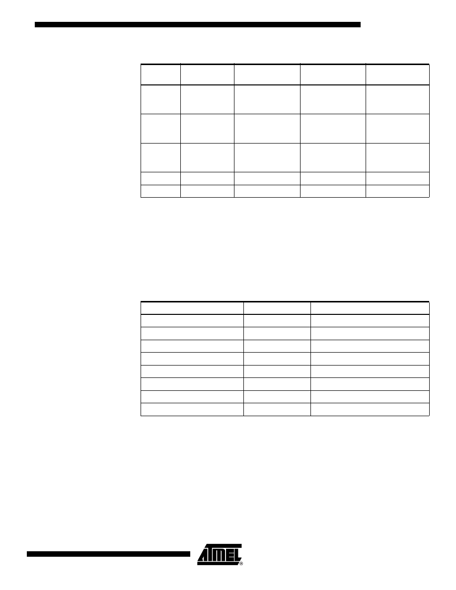
ATtiny15L Reset Sources
The ATtiny15L has four sources of Reset:
•
Power-on Reset. The MCU is reset when the supply voltage is below the Power-on
Reset threshold (V
POR
).
•
External Reset. The MCU is reset when a low-level is present on the RESET pin for
more than 500 ns.
•
Watchdog Reset. The MCU is reset when the Watchdog Timer period expires, and
the Watchdog is enabled.
•
Brown-out Reset. The MCU is reset when the supply voltage V
CC
is below the
Brown-out Reset threshold (V
BOT
).
During Reset, all I/O Registers are then set to their initial values, and the program starts
execution from address $000. The instruction placed in address $000 must be an RJMP
(relative jump) instruction to the reset handling routine. If the program never enables an
interrupt source, the Interrupt Vectors are not used, and regular program code can be
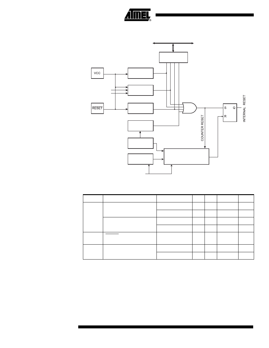
placed at these locations. The circuit diagram in Figure 12 shows the reset logic. Table 4
and Table 5 define the timing and electrical parameters of the reset circuitry. Note that
the Register File is unchanged by a reset.
14
ATtiny15L
1187F–AVR–06/05
Figure 12. Reset Logic
Note:
1. The Power-on Reset will not work unless the supply voltage has been below V
POT
(falling).
Table 4. Reset Characteristics (V
CC
= 5.0V)
Symbol
Parameter
Condition
Min
Typ
Max
Units
V
POT
Power-on Reset Threshold
Voltage (rising)
BOD disabled
1.0
1.4
1.8
V
BOD enabled
1.7
2.2
2.7
V
Power-on Reset Threshold
Voltage (falling)
BOD disabled
0.4
0.6
0.8
V
BOD enabled
1.7
2.2
2.7
V
V
RST
RESET Pin Threshold
Voltage
–
–
0.85 V
CC
V
V
BOT
Brown-out Reset Threshold
Voltage
(BODLEVEL = 1)
2.3
2.7
2.9
V
(BODLEVEL = 0)
3.4
4.0
4.3
V
MCU Status
Register (MCUSR)
Brown-out
Reset Circuit
BODEN
BODLEVEL
Delay Counters
CKSEL[1:0]
CK
TIMEOUT
WDRF
BORF
EXTRF
PORF
DATA BUS
Tunable Internal
Oscillator
Watchdog
Oscillator
Watchdog
Timer
Reset Circuit
Power-on Reset
Circuit
15
ATtiny15L
1187F–AVR–06/05
Notes:
1. On Power-up, the start-up time is increased with typical 0.6 ms.
2. “0” means programmed, “1” means unprogrammed.
Table 5 shows the start-up times from Reset. When the CPU wakes up from Power-
down, only the clock-counting part of the start-up time is used. The Watchdog Oscillator
is used for timing the real-time part of the start-up time. The number Watchdog Oscilla-
tor cycles used for each time-out is shown in Table 6.
The frequency of the Watchdog Oscillator is voltage dependent as shown in the Electri-
cal Characteristics section on page 64. The device is shipped with CKSEL = “00”.
Power-on Reset
A Power-on Reset (POR) pulse is generated by an On-chip Detection circuit. The detec-
tion level is nominally defined in Table 4. The POR is activated whenever V
CC
is below
the detection level. The POR circuit can be used to trigger the Start-up Reset, as well as
detect a failure in supply voltage.
A Power-on Reset (POR) circuit ensures that the device is Reset from Power-on.
Reaching the Power-on Reset threshold voltage invokes a delay counter, which deter-
mines the delay, for which the device is kept in RESET after V
CC
rise. The Time-out
period of the delay counter can be defined by the user through the CKSEL Fuses. The
different selections for the delay period are presented in Table 5. The RESET signal is
activated again, without any delay, when the V
CC
decreases below detection level.
Table 5. Reset Delay Selections
BODEN
Start-up Time,
t
TOUT
at V
CC
= 2.7V
Start-up Time,
t
TOUT
at V
CC
= 5.0V
Recommended
Usage
x
00
256 ms + 18 CK
64 ms + 18 CK
BOD disabled,
slowly rising
power
x
01
256 ms + 18 CK
64 ms + 18 CK
BOD disabled,
slowly rising
power
x
10
16 ms + 18 CK
4 ms + 18 CK
BOD disabled,
quickly rising
power
1
11
18 CK + 32 µs
18 CK + 8 µs
BOD disabled
0
11
18 CK + 128 µs
18 CK + 32 µs
BOD enabled
Table 6. Number of Watchdog Oscillator Cycles
V
CC
Conditions
Time-out
Number of Cycles
2.7V
32 µs
8
2.7V
128 µs
32
2.7V
16 ms
4K
2.7V
256 ms
64K
5.0V
8 µs
8
5.0V
32 µs
32
5.0V
4 ms
4K
5.0V
64 ms
64K

16
ATtiny15L
1187F–AVR–06/05
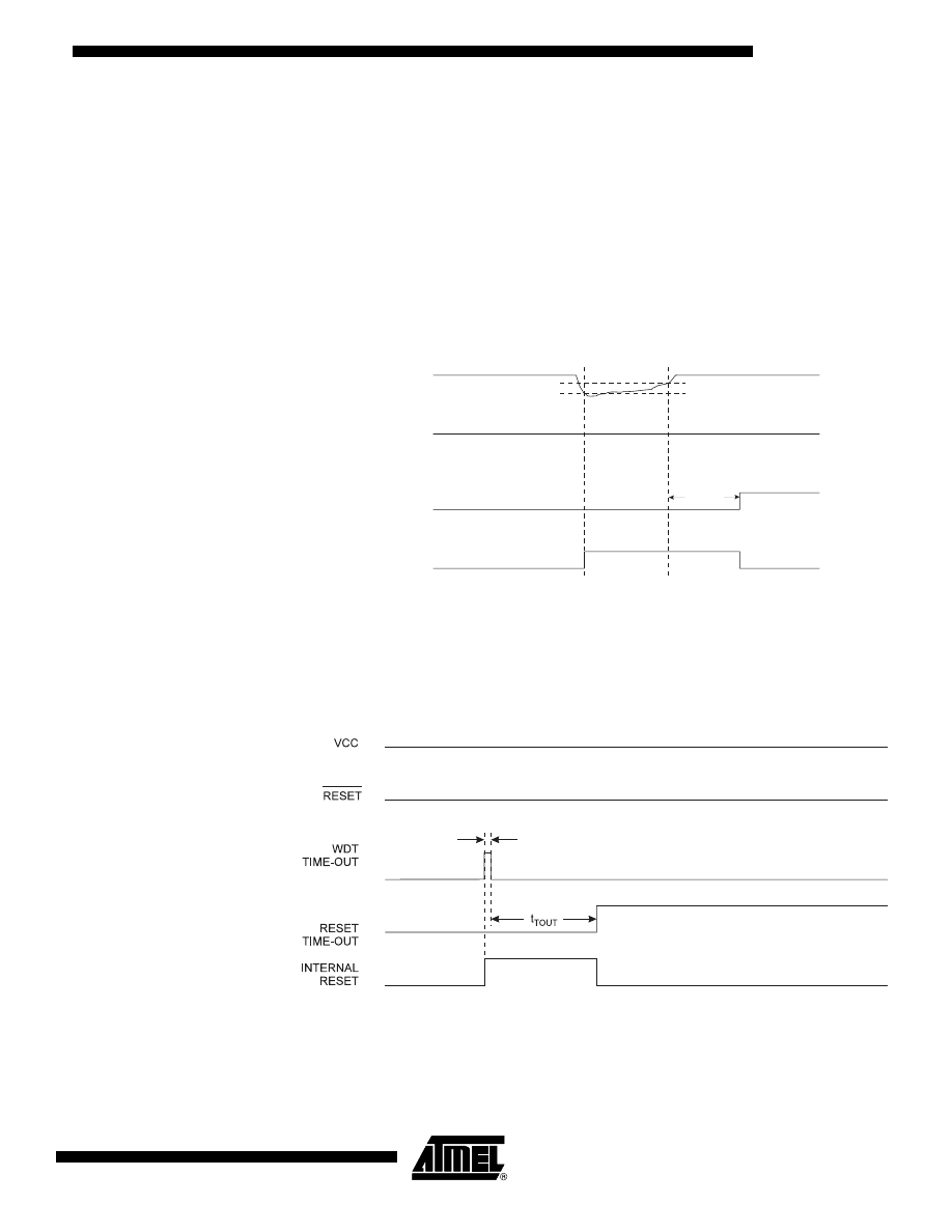
Figure 13. “MCU Start-up, RESET Tied to V
CC
Figure 14. MCU Start-up, RESET Extended Externally
External Reset
An External Reset is generated by a low-level on the RESET pin. Reset pulses longer
than 500 ns will generate a reset, even if the clock is not running. Shorter pulses are not
guaranteed to generate a reset. When the applied signal reaches the Reset Threshold
Voltage (V
RST
) on its positive edge, the delay timer starts the MCU after the Time-out
period t
TOUT
has expired.
Figure 15. External Reset during Operation
VCC
RESET
TIME-OUT
INTERNAL
RESET
t
TOUT
V
POT
V
RST
VCC
RESET
TIME-OUT
INTERNAL
RESET
t
TOUT
V
POT
V
RST
17
ATtiny15L
1187F–AVR–06/05
Brown-out Detection
ATtiny15L has an On-chip Brown-out Detection (BOD) circuit for monitoring the V
CC
level during the operation. The BOD circuit can be enabled/disabled by the fuse
BODEN. When BODEN is enabled (BODEN programmed), and V
CC
decreases below
the trigger level, the Brown-out Reset is immediately activated. When V
CC
increases
above the trigger level, the Brown-out Reset is deactivated after a delay. The delay is
defined by the user in the same way as the delay of POR signal, in Table 5. The trigger
level for the BOD can be selected by the fuse BODLEVEL to be 2.7V (BODLEVEL
unprogrammed), or 4.0V (BODLEVEL programmed). The trigger level has a hysteresis
of 50 mV to ensure spike-free Brown-out Detection.
The BOD circuit will only detect a drop in V
CC
if the voltage stays below the trigger level
for longer than 3
µs
for trigger level 4.0V, 7
µs
for trigger level 2.7V (typical values).
Figure 16. Brown-out Reset during Operation
Note:
1. The hysteresis on V
BOT
: V
BOT+
= V
BOT
+ 25 mV, V
BOT-
= V
BOT
- 25 mV.
Watchdog Reset
When the Watchdog times out, it will generate a short reset pulse of one CK cycle dura-
tion. On the falling edge of this pulse, the delay timer starts counting the Time-out period
t
TOUT
. Refer to page 34 for details on operation of the Watchdog Timer.
Figure 17. Watchdog Reset during Operation
V
CC
RESET
TIME-OUT
INTERNAL
RESET
V
BOT-
V
BOT+
t
TOUT
1 CK Cycle

18
ATtiny15L
1187F–AVR–06/05
MCU Status Register –
MCUSR
The MCU Status Register provides information on which reset source caused an MCU
Reset.
• Bit 7..4 – Res: Reserved Bits
These bits are reserved bits in the ATtiny15L and always read as zero.
• Bit 3 – WDRF: Watchdog Reset Flag
This bit is set (one) if a Watchdog Reset occurs. The bit is reset (zero) by a Power-on
Reset, or by writing a logical “0” to the flag.
• Bit 2 – BORF: Brown-out Reset Flag
This bit is set (one) if a Brown-out Reset occurs. The bit is reset (zero) by a Power-on
Reset, or by writing a logical “0” to the flag.
• Bit 1 – EXTRF: External Reset Flag
This bit is set (one) if a External Reset occurs. The bit is reset (zero) by a Power-on
Reset, or by writing a logical “0” to the flag.
• Bit 0 – PORF: Power-on Reset Flag
This bit is set (one) if a Power-on Reset occurs. The bit is reset (zero) by writing a logical
“0” to the flag.
To make use of the Reset Flags to identify a reset condition, the user should read and
then reset the MCUSR as early as possible in the program. If the register is cleared
before another reset occurs, the source of the reset can be found by examining the
Reset Flags.
Internal Voltage
Reference
ATtiny15L features an internal bandgap reference with a nominal voltage of 1.22V. This
reference is used for Brown-out Detection, and it can be used as an input to the Analog
Comparator. The 2.56V reference to the ADC is generated from the internal bandgap
reference.
Voltage Reference Enable
Signals and Start-up Time
The voltage reference has a start-up time that may influence the way it should be used.
The maximum start-up time is 10 µs. To save power, the reference is not always turned
on. The reference is on during the following situations:
1.
When the BOD is enabled (by programming the BODEN Fuse).
2.
When the bandgap reference is connected to the Analog Comparator (by setting
the AINBG bit in ACSR).
3.
When the ADC is enabled.
Thus, when the BOD is not enabled, after setting the AINBG bit, the user must always
allow the reference to start-up before the output from the Analog Comparator is used.
The bandgap reference uses typically 10 µA, and to reduce power consumption in
Power-down mode, the user can avoid the three conditions above to ensure that the ref-
erence is turned off before entering Power-down mode.
Bit
7
6
5
4
3
2
1
0
$34
–
–
–
–
WDRF
BORF
EXTRF
PORF
MCUSR
Read/Write
R
R
R
R
R/W
R/W
R/W
R/W
Initial Value
0
0
0
0
See Bit Description

19
ATtiny15L
1187F–AVR–06/05
Interrupt Handling
The ATtiny15L has two 8-bit Interrupt Mask Control Registers: GIMSK (General Inter-
rupt Mask Register) and TIMSK (Timer/Counter Interrupt Mask Register).
When an interrupt occurs, the Global Interrupt Enable I-bit is cleared (zero) and all inter-
rupts are disabled. The user software can set the I-bit (one) to enable interrupts. The I-
bit is set (one) when a Return from Interrupt instruction (RETI) is executed.
When the Program Counter is vectored to the actual Interrupt Vector in order to execute
the interrupt handling routine, hardware clears the corresponding flag that generated the
interrupt. Some of the interrupt flags can also be cleared by writing a logical “1” to the
flag bit position(s) to be cleared.
If an interrupt condition occurs when the corresponding interrupt enable bit is cleared
(zero), the interrupt flag will be set and remembered until the interrupt is enabled, or the
flag is cleared by software.
If one or more interrupt conditions occur when the global interrupt enable bit is cleared
(zero), the corresponding interrupt flag(s) will be set and remembered until the global
interrupt enable bit is set (one), and will be executed by order of priority.
Note that external level interrupt does not have a flag, and will only be remembered for
as long as the interrupt condition is present.
Note that the Status Register is not automatically stored when entering an interrupt rou-
tine and restored when returning from an interrupt routine. This must be handled by
software.
Interrupt Response Time
The interrupt execution response for all the enabled AVR interrupts is four clock cycles
minimum. After the four clock cycles the Program Vector address for the actual interrupt
handling routine is executed. During this 4-clock-cycle period, the Program Counter
(nine bits) is pushed onto the Stack. The vector is often a relative jump to the interrupt
routine, and this jump takes two clock cycles. If an interrupt occurs during execution of a
multi-cycle instruction, this instruction is completed before the interrupt is served. If an
interrupt occurs when the MCU is in sleep mode, the interrupt execution response time
is increased by four clock cycles.
A return from an interrupt handling routine takes four clock cycles. During these four
clock cycles, the Program Counter (nine bits) is popped back from the Stack. When
AVR exits from an interrupt, it will always return to the main program and execute one
more instruction before any pending interrupt is served.
The General Interrupt Mask
Register – GIMSK
• Bit 7 – Res: Reserved Bit
This bit is a reserved bit in the ATtiny15L and always reads as zero.
• Bit 6 – INT0: External Interrupt Request 0 Enable
When the INT0 bit is set (one) and the I-bit in the Status Register (SREG) is set (one),
the external pin interrupt is activated. The Interrupt Sense Control0 bits 1/0 (ISC01 and
ISC00) in the MCU general Control Register (MCUCR) define whether the external
interrupt is activated on rising or falling edge, on pin change, or low level of the INT0 pin.
Activity on the pin will cause an interrupt request even if INT0 is configured as an output.
Bit
7
6
5
4
3
2
1
0
$3B
–
INT0
PCIE
–
–
–
–
–
GIMSK
Read/Write
R
R/W
R/W
R
R
R
R
R
Initial Value
0
0
0
0
0
0
0
0

20
ATtiny15L
1187F–AVR–06/05
The corresponding interrupt of External Interrupt Request 0 is executed from Program
memory address $001. See also “External Interrupts.”
• Bit 5 – PCIE: Pin Change Interrupt Enable
When the PCIE bit is set (one) and the I-bit in the Status Register (SREG) is set (one),
the interrupt on pin change is enabled. Any change on any input or I/O pin will cause an
interrupt. The corresponding interrupt of Pin Change Interrupt Request is executed from
Program memory address $002. See also “Pin Change Interrupt.”
• Bits 4..0 – Res: Reserved Bits
These bits are reserved bits in the ATtiny15L and always read as zero.
The General Interrupt Flag
Register – GIFR
• Bit 7 – Res: Reserved Bit
This bit is a reserved bit in the ATtiny15L and always reads as zero.
• Bit 6 – INTF0: External Interrupt Flag0
When an edge or logic change on the INT0 pin triggers an interrupt request, INTF0
becomes set (one). If the I-bit in SREG and the INT0 bit in GIMSK are set (one), the
MCU will jump to the Interrupt Vector at address $001. The flag is cleared when the
interrupt routine is executed. Alternatively, the flag can be cleared by writing a logical “1”
to it. The flag is always cleared when INT0 is configured as level interrupt.
• Bit 5 – PCIF: Pin Change Interrupt Flag
When an event on any input or I/O pin triggers an interrupt request, PCIF becomes set
(one). If the I-bit in SREG and the PCIE bit in GIMSK are set (one), the MCU will jump to
the Interrupt Vector at address $002. The flag is cleared when the interrupt routine is
executed. Alternatively, the flag can be cleared by writing a logical “1” to it.
• Bits 4..0 – Res: Reserved Bits
These bits are reserved bits in the ATtiny15L and always read as zero.
The Timer/Counter Interrupt
Mask Register – TIMSK
• Bit 7 – Res: Reserved Bit
This bit is a reserved bit in the ATtiny15L and always reads as zero.
• Bit 6 – OCIE1A: Timer/Counter1 Output Compare Interrupt Enable
When the OCIE1A bit is set (one) and the I-bit in the Status Register is set (one), the
Timer/Counter1 Compare Match, interrupt is enabled. The corresponding interrupt (at
Bit
7
6
5
4
3
2
1
0
$3A
–
INTF0
PCIF
–
–
–
–
–
GIFR
Read/Write
R
R/W
R/W
R
R
R
R
R
Initial Value
0
0
0
0
0
0
0
0
Bit
7
6
5
4
3
2
1
0
$39
–
OCIE1A
–
–
–
TOIE1
TOIE0
–
TIMSK
Read/Write
R
R/W
R
R
R
R/W
R/W
R
Initial Value
0
0
0
0
0
0
0
0

21
ATtiny15L
1187F–AVR–06/05
vector $003) is executed if a compare match A in Timer/Counter1 occurs, i.e., when the
OCF1A bit is set (one) in the Timer/Counter Interrupt Flag Register (TIFR).
• Bit 5..3 – Res: Reserved Bits
These bits are reserved bits in the ATtiny15L and always read as zero.
• Bit 2 – TOIE1: Timer/Counter1 Overflow Interrupt Enable
When the TOIE1 bit is set (one) and the I-bit in the Status Register is set (one), the
Timer/Counter1 Overflow interrupt is enabled. The corresponding interrupt (at vector
$004) is executed if an overflow in Timer/Counter1 occurs, i.e., when the TOV1 bit is set
(one) in the Timer/Counter Interrupt Flag Register (TIFR).
• Bit 1 – TOIE0: Timer/Counter0 Overflow Interrupt Enable
When the TOIE0 bit is set (one) and the I-bit in the Status Register is set (one), the
Timer/Counter0 Overflow interrupt is enabled. The corresponding interrupt (at vector
$005) is executed if an overflow in Timer/Counter0 occurs, i.e., when the TOV0 bit is set
(one) in the Timer/Counter Interrupt Flag Register (TIFR).
• Bit 0 – Res: Reserved Bit
This bit is a reserved bit in the ATtiny15L and always reads as zero.
The Timer/Counter Interrupt
Flag Register – TIFR
• Bit 7 – Res: Reserved Bit
This bit is a reserved bit in the ATtiny15L and always reads as zero.
• Bit 6 – OCF1A: Output Compare Flag 1A
The OCF1A bit is set (one) when compare match occurs between Timer/Counter1 and
the data value in OCR1A (Output Compare Register 1A). OCF1A is cleared by hard-
ware when executing the corresponding interrupt handling vector. Alternatively, OCF1A
is cleared by writing a logical “1” to the flag. When the I-bit in SREG, OCIE1A, and
OCF1A are set (one), the Timer/Counter1 compare match A interrupt is executed.
• Bits 5..3 – Res: Reserved bits
These bits are reserved bits in the ATtiny15L and always read as zero.
• Bit 2 – TOV1: Timer/Counter1 Overflow Flag
The bit TOV1 is set (one) when an overflow occurs in Timer/Counter1. TOV1 is cleared
by hardware when executing the corresponding interrupt handling vector. Alternatively,
TOV1 is cleared by writing a logical “1” to the flag. When the SREG I-bit, TOIE1
( T i m e r / C o u n t e r 1 O v e r f l o w I n t e r r u p t E n a b l e ) a n d T O V 1 a r e s e t ( o n e ) , t h e
Timer/Counter1 Overflow Interrupt is executed.
Bit
7
6
5
4
3
2
1
0
$38
–
OCF1A
–
–
–
TOV1
TOV0
–
TIFR
Read/Write
R
R/W
R
R
R
R/W
R/W
R
Initial Value
0
0
0
0
0
0
0
0

22
ATtiny15L
1187F–AVR–06/05
• Bit 1 – TOV0: Timer/Counter0 Overflow Flag
The bit TOV0 is set (one) when an overflow occurs in Timer/Counter0. TOV0 is cleared
by hardware when executing the corresponding interrupt handling vector. Alternatively,
TOV0 is cleared by writing a logical “1” to the flag. When the SREG I-bit, TOIE0
( T i m e r / C o u n t e r 0 O v e r f l o w I n t e r r u p t E n a b l e ) a n d T O V 0 a r e s e t ( o n e ) , t h e
Timer/Counter0 Overflow interrupt is executed.
• Bit 0 – Res: Reserved Bit
This bit is a reserved bit in the ATtiny15L and always reads as zero.
External Interrupt
The External Interrupt is triggered by the INT0 pin. Observe that, if enabled, the interrupt
will trigger even if the INT0 pin is configured as an output. This feature provides a way of
generating a software interrupt. The External Interrupt can be triggered by a falling or
rising edge, a pin change, or a low level. This is set up as indicated in the specification
for the MCU Control Register (MCUCR). When the external interrupt is enabled and is
configured as level-triggered, the interrupt will trigger as long as the pin is held low.
The External Interrupt is set up as described in the specification for the MCU Control
Register (MCUCR).
Pin Change Interrupt
The pin change interrupt is triggered by any change in logical value on any input or I/O
pin. Change on pins PB4..0 will always cause an interrupt. Change on pin PB5 will
cause an interrupt if the pin is configured as input or I/O, as described in the section “Pin
Descriptions” on page 4. Observe that, if enabled, the interrupt will trigger even if the
changing pin is configured as an output. This feature provides a way of generating a
software interrupt. Also observe that the pin change interrupt will trigger even if the pin
activity triggers another interrupt, for example the external interrupt. This implies that
one external event might cause several interrupts. The values on the pins are sampled
before detecting edges. If pin change interrupt is enabled, pulses that last longer than
one CPU clock period will generate an interrupt. Shorter pulses are not guaranteed to
generate an interrupt.
The MCU Control Register –
MCUCR
The MCU Control Register contains control bits for general MCU functions.
• Bits 7 – Res: Reserved Bit
This bit is a reserved bit in the ATtiny15L and always reads as zero.
• Bit 6- PUD: Pull-up Disable
This PUD bit must be set (one) to disable internal pull-up registers at Port B.
• Bit 5 – SE: Sleep Enable
The SE bit must be set (one) to make the MCU enter the sleep mode when the SLEEP
instruction is executed. To avoid the MCU entering the sleep mode unless it is the pro-
grammer’s purpose, it is recommended to set the Sleep Enable SE bit just before the
execution of the SLEEP instruction.
Bit
7
6
5
4
3
2
1
0
$35
–
PUD
SE
SM1
SM0
–
ISC01
ISC00
MCUCR
Read/Write
R
R/W
R/W
R/W
R/W
R
R/W
R/W
Initial Value
0
0
0
0
0
0
0
0
23
ATtiny15L
1187F–AVR–06/05
• Bits 4, 3 – SM1, SM0: Sleep Mode Select Bits 1 and 0
These bits select between the three available sleep modes, as shown in Table 7.
For details, refer to “Sleep Modes” below.
• Bit 2 – Res: Reserved Bit
This bit is a reserved bit in the ATtiny15L and always reads as zero.
• Bits 1, 0 – ISC01, ISC00: Interrupt Sense Control 0 Bit 1 and Bit 0
The External Interrupt 0 is activated by the external pin INT0 if the SREG I-flag and the
corresponding interrupt mask is set (one). The activity on the external INT0 pin that acti-
vates the interrupt is defined in Table 8:
Note:
1. When changing the ISC10/ISC00 bits, INT0 must be disabled by clearing its Interrupt
Enable bit in the GIMSK Register. Otherwise an interrupt can occur when the bits are
changed.
Sleep Modes
To enter any of the three sleep modes, the SE bit in MCUCR must be set (one) and a
SLEEP instruction must be executed. The SM1 and SM0 bits in the MCUCR Register
select which sleep mode (Idle, ADC Noise Reduction or Power-down) will be activated
by the SLEEP instruction (see Table 7). If an enabled interrupt occurs while the MCU is
in a sleep mode, the MCU wakes up. The MCU is then halted for four cycles, executes
the interrupt routine and resumes execution from the instruction following SLEEP. On
wake-up from Power-down mode on pin change, two instruction cycles are executed
before the Pin Change Interrupt Flag is updated. The contents of the Register File,
SRAM, and I/O memory are unaltered when the device wakes up from sleep. If a reset
occurs during sleep mode, the MCU wakes up and executes from the Reset Vector.
Idle Mode
When the SM1/SM0 bits are “00”, the SLEEP instruction forces the MCU into the Idle
mode, stopping the CPU but allowing the ADC, Analog Comparator, Timer/Counters,
Watchdog and the Interrupt system to continue operating. This enables the MCU to
wake-up from external triggered interrupts as well as internal ones like the Timer Over-
flow Interrupt and Watchdog Reset. If the ADC is enabled, a conversion starts
automatically when this mode is entered. If wake-up from the Analog Comparator inter-
rupt is not required, the Analog Comparator can be powered down by setting the ADC-
bit in the Analog Comparator Control and Status Register (ACSR). This will reduce
power consumption in Idle mode.
Table 7. Sleep Modes
SM1
SM0
Sleep Mode
0
0
Idle mode
0
1
ADC Noise Reduction mode
1
0
Power-down mode
1
1
Reserved
Table 8. Interrupt 0 Sense Control
ISC01
ISC00
Description
0
0
The low level of INT0 generates an interrupt request.
0
1
Any change on INT0 generates an interrupt request
1
0
The falling edge of INT0 generates an interrupt request.
1
1
The rising edge of INT0 generates an interrupt request.

24
ATtiny15L
1187F–AVR–06/05
ADC Noise Reduction Mode
When the SM1/SM0 bits are “01”, the SLEEP instruction forces the MCU into the ADC
Noise Reduction mode, stopping the CPU but allowing the ADC, the external interrupt
pin, pin change interrupt and the Watchdog (if enabled) to continue operating. Please
note that the clock system including the PLL is also active in the ADC Noise Reduction
mode. This improves the noise environment for the ADC, enabling higher resolution
measurements. If the ADC is enabled, a conversion starts automatically when this mode
is entered. In addition to Watchdog Time-out and External Reset, only an external level-
triggered interrupt, a pin change interrupt or an ADC interrupt can wake up the MCU.
Power-down Mode
When the SM1/SM0 bits are “10”, the SLEEP instruction forces the MCU into the Power-
down mode. Only an External Reset, a Watchdog Reset (if enabled), an external level-
triggered interrupt, or a pin change interrupt can wake up the MCU.
Note that if a level-triggered or pin change interrupt is used for wake-up from Power-
down mode, the changed level must be held for some time to wake up the MCU. This
makes the MCU less sensitive to noise. The changed level is sampled twice by the
Watchdog Oscillator clock, and if the input has the required level during this time, the
MCU will wake up. The period of the Watchdog Oscillator is 2.9
µs
(nominal) at 3.0V and
25
°C. The frequency of the Watchdog Oscillator is voltage-dependent as shown in the
“Electrical Characteristics” section.
When waking up from the Power-down mode, a delay from the wake-up condition
occurs until the wake-up becomes effective. This allows the clock to restart and become
stable after having been stopped. The wake-up period is defined by the same CKSEL
Fuses that define the Reset Time-out period.
Tuneable Internal RC
Oscillator
The internal RC Oscillator provides a fixed 1.6 MHz clock (nominal at 5V and 25
°C).
This internal clock is always the system clock of the ATtiny15L. This Oscillator can be
calibrated by writing the calibration byte (see page 55) to the OSCCAL Register.
The System Clock Oscillator
Calibration Register –
OSCCAL
Writing the calibration byte to this address will trim the internal Oscillator frequency in
order to remove process variations. When OSCCAL is zero (initial value), the lowest
available frequency is chosen. Writing non-zero values to this register will increase the
frequency of the internal oscillator. Writing $FF to the register selects the highest avail-
able frequency.
Internal PLL for Fast
Peripheral Clock
Generation
The internal PLL in ATtiny15L generates a clock frequency that is 16x multiplied from
the RC Oscillator system clock. If the RC Oscillator frequency is the nominal 1.6 MHz,
the fast peripheral clock is 25.6 MHz. The fast peripheral clock, or a clock prescaled
from that, can be selected as the clock source for Timer/Counter1.
The PLL is locked on the tunable internal RC Oscillator and adjusting the tunable inter-
nal RC oscillator via the OSCCAL Register will adjust the fast peripheral clock at the
same time. Timer1 may malfunction if the internal RC oscillator is adjusted beyond 1.75
MHz.
It is recommended not to take the OSCCAL adjustments to a higher frequency than
1.75 MHz in order to keep proper operation of all chip functions.
Bit
7
6
5
4
3
2
1
0
$31
CAL7
CAL6
CAL5
CAL4
CAL3
CAL2
CAL1
CAL0
OSCCAL
Read/Write
R/W
R/W
R/W
R/W
R/W
R/W
R/W
R/W
Initial Value
0
0
0
0
0
0
0
0
25
ATtiny15L
1187F–AVR–06/05
Timer/Counters
The ATtiny15L provides two general purpose 8-bit Timer/Counters. The Timer/Counters
h a v e s e p a r a t e p r e s c a l i n g s e l e c t i o n f r o m s e p a r a t e 1 0 - b i t p r e s c a l e r s . T h e
Timer/Counter0 uses internal clock (CK) as the clock time base. The Timer/Counter1
may use either the internal clock (CK) or the fast peripheral clock (PCK) as the clock
time base.
The Timer/Counter0
Prescaler
Figure 18 shows the Timer/Counter prescaler.
Figure 18. Timer/Counter0 Prescaler
The four prescaled selections are: CK/8, CK/64, CK/256, and CK/1024, where CK is the
Oscillator clock. CK, external source and stop, can also be selected as clock sources.
Setting the PSR10 bit in SFIOR resets the prescaler. This allows the user to operate
with a predictable prescaler.
The Timer/Counter1
Prescaler
Figure 19 shows the Timer/Counter1 prescaler. For Timer/Counter1 the clock selections
are: PCK, PCK/2, PCK/4, PCK/8, CK (=PCK/16), CK/2, CK/4, CK/8,CK/16, CK/32,
CK/64, CK/128, CK/256, CK/512, CK/1024, and stop. The clock options are described in
Table 12 on page 31 and the Timer/Counter1 Control Register (TCCR1). Setting the
PSR1 bit in the SFIOR Register resets the 10-bit prescaler. This allows the user to oper-
ate with a predictable prescaler.
Figure 19. Timer/Counter1 Prescaler
10-BIT T/C PRESCALER
0
TIMER/COUNTER0 CLOCK SOURCE
CK
T0
PSR0
CLEAR
CS00
TCK0
CS01
CS02
CK/8
CK/256
CK/1024
CK/64
10-BIT T/C PRESCALER
TIMER/COUNTER1 CLOCK SOURCE
CK
PSR1
CS10
CS11
CS12
CK/8
CK/256
CK/1024
CK/64
PCK
(25.6 MHz)
(1.6 MHz)
0
CS13
CLEAR
CLEAR
3-BIT T/C PRESCALER
PCK/2
PCK/4
PCK/8
CK (=PCK/16)
CK/2
CK/4
CK/16
CK/32
CK/128
CK/512

26
ATtiny15L
1187F–AVR–06/05
The Special Function IO
Register – SFIOR
• Bit 7..3 – Res: Reserved Bits
These bits are reserved bits in the ATtiny15L and always read as zero.
• Bit 2 – FOC1A: Force Output Compare 1A
Writing a logical “1” to this bit forces a change in the Compare Match Output pin PB1
(OC1A) according to the values already set in COM1A1 and COM1A0. The Force Out-
put Compare bit can be used to change the output pin without waiting for a compare
match in timer. The automatic action programmed in COM1A1 and COM1A0 happens
as if a Compare Match had occurred, but no interrupt is generated and the
Timer/Counter1 will not be cleared even if CTC1 is set. The FOC1A bit will always be
read as zero. The setting of the FOC1A bit has no effect in PWM mode.
• Bit 1 – PSR1: Prescaler Reset Timer/Counter1
When this bit is set (one) the Timer/Counter1 prescaler will be reset. The bit will be
cleared by hardware after the operation is performed. Writing a “0” to this bit will have no
effect. This bit will always be read as zero.
• Bit 0 – PSR0: Prescaler Reset Timer/Counter0
When this bit is set (one) the Timer/Counter0 prescaler will be reset. The bit will be
cleared by hardware after the operation is performed. Writing a “0” to this bit will have no
effect. This bit will always be read as zero.
The 8-bit Timer/Counter0
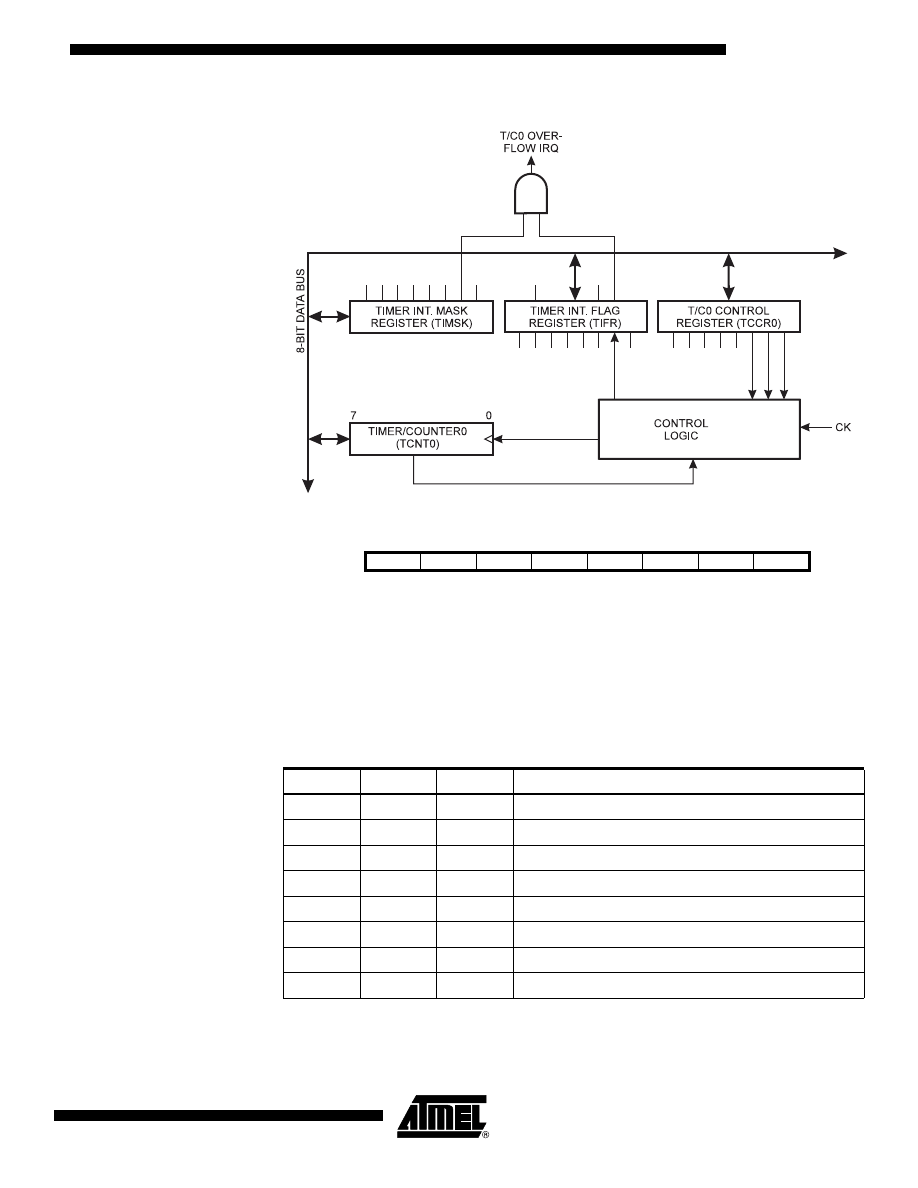
Figure 20 shows the block diagram for Timer/Counter0.
The 8-bit Timer/Counter0 can select clock source from CK, prescaled CK or an external
pin. In addition, it can be stopped as described in the specification for the
Timer/Counter0 Control Register (TCCR0). The Overflow Status Flag is found in the
Timer/Counter Interrupt Flag Register (TIFR). Control signals are found in the
Timer/Counter0 Control Register (TCCR0). The interrupt enable/disable settings for
Timer/Counter0 are found in the Timer/Counter Interrupt Mask Register (TIMSK).
When Timer/Counter0 is externally clocked, the external signal is synchronized with the
oscillator frequency of the CPU. To ensure proper sampling of the external clock, the
minimum time between two external clock transitions must be at least one internal CPU
clock period. The external clock signal is sampled on the rising edge of the internal CPU
clock.
The 8-bit Timer/Counter0 features both a high-resolution and a high-accuracy usage
with the lower prescaling opportunities. Similarly, the high-prescaling opportunities
make the Timer/Counter0 useful for lower-speed functions or exact-timing functions with
infrequent actions.
Bit
7
6
5
4
3
2
1
0
$2C
–
–
–
–
–
FOC1A
PSR1
PSR0
SFIOR
Read/Write
R
R
R
R
R
R/W
R/W
R/W
Initial Value
0
0
0
0
0
0
0
0
27
ATtiny15L
1187F–AVR–06/05
Figure 20. Timer/Counter0 Block Diagram
The Timer/Counter0 Control
Register – TCCR0
• Bits 7..3 – Res: Reserved Bits
These bits are reserved bits in the ATtiny15L and always read as zero.
• Bits 2, 1, 0 – CS02, CS01, CS00: Clock Select0, Bits 2, 1 and 0
The Clock Select0 bits 2, 1 and 0 define the prescaling source of Timer0.
The Stop condition provides a Timer Enable/Disable function. The prescaled CK modes
are scaled directly from the CK Oscillator clock. If the external pin modes are used for
Timer/Counter0, transitions on PB2/(T0) will clock the counter even if the pin is config-
ured as an output. This feature can give the user SW control of counting.
OCIE1A
T
OIE1
T
OIE0
TO
V
0
TO
V
0
CS02
CS01
CS00
TO
V
1
OCF1A
T/C CLK SOURCE
Bit
7
6
5
4
3
2
1
0
$33
–
–
–
–
–
CS02
CS01
CS00
TCCR0
Read/Write
R
R
R
R
R
R/W
R/W
R/W
Initial Value
0
0
0
0
0
0
0
0
Table 9. Clock 0 Prescale Select
CS02
CS01
CS00
Description
0
0
0
Stop, the Timer/Counter0 is stopped.
0
0
1
CK
0
1
0
CK/8
0
1
1
CK/64
1
0
0
CK/256
1
0
1
CK/1024
1
1
0
External Pin T0, falling edge
1
1
1
External Pin T0, rising edge
28
ATtiny15L
1187F–AVR–06/05
The Timer Counter 0 – TCNT0
The Timer/Counter0 is implemented as an up-counter with read and write access. If the
Timer/Counter0 is written and a clock source is present, the Timer/Counter0 continues
counting in the timer clock cycle following the write operation.
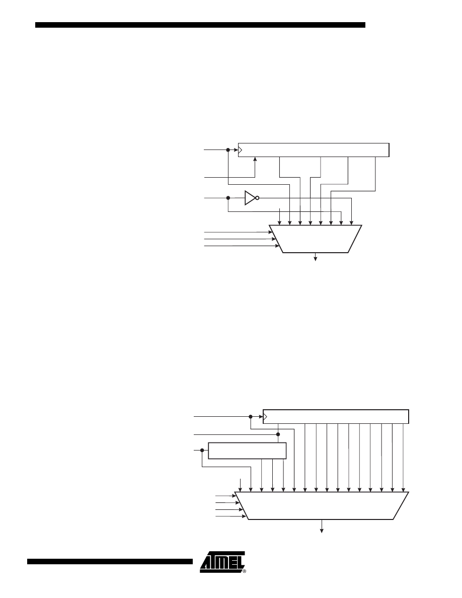
The 8-bit Timer/Counter1
This module features a high-resolution and a high-accuracy usage with the lower pres-
caling opportunities. Timer/Counter1 can also be used as an accurate, high speed, 8-bit
Pulse Width Modulator (PWM) using clock speeds up to 25.6 MHz. In this mode,
Timer/Counter1 and the Output Compare Registers serve as a standalone PWM. Refer
to page 34 for a detailed description of this function. Similarly, the high-prescaling
opportunities make this unit useful for lower-speed functions or exact-timing functions
with infrequent actions.
Figure 21 shows the block diagram for Timer/Counter1.
Figure 21. Timer/Counter1 Block Diagram
The two Status Flags (Overflow and Compare Match) are found in the Timer/Counter
Interrupt Flag Register (TIFR). Control signals are found in the Timer/Counter Control
Register (TCCR1). The interrupt enable/disable settings are found in the Timer/Counter
Interrupt Mask Register (TIMSK).
Bit
7
6
5
4
3
2
1
0
$32
MSB
LSB
TCNT0
Read/Write
R/W
R/W
R/W
R/W
R/W
R/W
R/W
R/W
Initial Value
0
0
0
0
0
0
0
0
8-BIT DATA BUS
TIMER INT. FLAG
REGISTER (TIFR)
TIMER/COUNTER1
(TCNT1)
8-BIT COMPARATOR
T/C1 OUTPUT
T/C1 OUTPUT
COMPARE REGISTER A
COMPARE REGISTER B
TIMER INT. MASK
REGISTER (TIMSK)
T/C CLEAR
T/C1 CONTROL
LOGIC
TOV1
OCF1A
OCF1A
TOV1
TOIE0
TOIE1
OCIE1A
CK
PCK
T/C1 OVER-
FLOW IRQ
T/C1 A COMPARE
MATCH IRQ
T/C CONTROL
REGISTER 1 (TCCR1)
CS12
COM1A1
PWM1
CS11
COM1A0
CS10
CS13
(OCR1A)
8-BIT COMPARATOR
(OCR1B)
SFIOR
TOV0
FOC1
PSR1
CTC1
T/C1 OC1A PIN/
PORT PB1
(PWM OUTPUT)
PSR0
29
ATtiny15L
1187F–AVR–06/05
The Timer/Counter1 contains two Output Compare Registers, OCR1A and OCR1B, as
the data source to be compared with the Timer/Counter1 contents. In Normal mode the
Output Compare function is operational with OCR1A only, and the Output Compare
function includes optional clearing of the counter on compare match, and action on the
Output Compare pin (PB1) (OC1A).
In PWM mode OCR1A provides the data value against which the Timer/Counter value is
compared. Upon compare match the PWM output is generated. In PWM mode The
Timer/Counter counts up to the value specified in Output Compare Register OCR1B
and starts again from $00. This feature allows limiting the counter “full” value to a speci-
fied value, lower than $FF. However, if OCR1n is $00, the output will remain constant
and not toggle at all. If OCR1n equals $01, the pulse width will be two ticks, increasing
linearly if OCR1n is larger than $01. Together with the many prescaler options, flexible
PWM frequency selection is provided. Table 14 lists clock selection and OCR1B values
to obtain PWM frequencies from 10 kHz to 150 kHz at 10 kHz steps.
In applications with variable PWM, halving the prescaler setting and doubling the duty
cycle can be used to fine-tune the PWM. Alternatively inverted PWM can be used.
The Timer/Counter1 Control
Register – TCCR1
• Bit 7 – CTC1: Clear Timer/Counter on Compare Match
When the CTC1 control bit is set (one), Timer/Counter1 is reset to $00 in the CPU clock
cycle after a compare match with OCR1A Register value. If the control bit is cleared,
Timer/Counter1 continues counting and is unaffected by a compare match.
• Bit 6 – PWM1: Pulse Width Modulator Enable
When set (one), this bit enables PWM mode for Timer/Counter1. This mode is described
on page 31.
• Bits 5,4 – COM1A1, COM1A0: Compare Output Mode, Bits 1 and 0
The COM1A1 and COM1A0 control bits determine any output pin action following a
compare match A in Timer/Counter1. Output pin actions affect pin PB1(OC1A). Since
this is an alternative function to an I/O port, the corresponding direction control bit must
be set (one) to control an output pin. The control configuration is shown in Table 10.
Note:
1. In PWM mode, these bits have a different function. Refer to Table 12 for a detailed
description.When changing the COM1A1/COM1A0 bits, the Output Compare 1A
Interrupt must be disabled by clearing its Interrupt Enable bit in the TIMSK Register.
Otherwise an interrupt can occur when the bits are changed.
Bit
7
6
5
4
3
2
1
0
$30
CTC1
PWM1
COM1A1
COM1A0
CS13
CS12
CS11
CS10
TCCR1
Read/Write
R/W
R/W
R/W
R/W
R/W
R/W
R/W
R/W
Initial Value
0
0
0
0
0
0
0
0
Table 10. Compare Mode Select
COM1A1
COM1A0
Description
0
0
Timer/Counter disconnected from output pin OC1A
0
1
Toggle the OC1A output line.
1
0
Clear the OC1A output line (to zero).
1
1
Set the OC1A output line (to one).

30
ATtiny15L
1187F–AVR–06/05
• Bits 3, 2, 1, 0 – CS13, CS12, CS11, CS10: Clock Select Bits 3, 2, 1, and 0
The Clock Select bits 3, 2, 1, and 0 define the prescaling source of Timer/Counter1.
The Stop condition provides a Timer Enable/Disable function. The prescaled CK modes
are scaled directly from the CK oscillator clock.
The Timer/Counter1 – TCNT1
This 8-bit register contains the value of Timer/Counter1.
Timer/Counter1 is implemented as an up-counter with read and write access. Due to
synchronization of the CPU and Timer/Counter1, data written into Timer/Counter1 is
delayed by one CPU clock cycle.
Table 11. Timer/Counter1 Prescale Select
CS13
CS12
CS11
CS10
Description
0
0
0
0
Timer/Counter1 is stopped.
0
0
0
1
CK*16 (=PCK)
0
0
1
0
CK*8 (=PCK/2)
0
0
1
1
CK*4 (=PCK/4)
0
1
0
0
CK*2 (=PCK/8)
0
1
0
1
CK
0
1
1
0
CK/2
0
1
1
1
CK/4
1
0
0
0
CK/8
1
0
0
1
CK/16
1
0
1
0
CK/32
1
0
1
1
CK/64
1
1
0
0
CK/128
1
1
0
1
CK/256
1
1
1
0
CK/512
1
1
1
1
CK/1024
Bit
7
6
5
4
3
2
1
0
$2F
MSB
LSB
TCNT1
Read/Write
R/W
R/W
R/W
R/W
R/W
R/W
R/W
R/W
Initial Value
0
0
0
0
0
0
0
0

31
ATtiny15L
1187F–AVR–06/05
Timer/Counter1 Output
Compare RegisterA – OCR1A
The Output Compare Register 1A is an 8-bit read/write register.
The Timer/Counter Output Compare Register 1A contains the data to be continuously
compared with Timer/Counter1. Actions on compare matches are specified in TCCR1. A
compare match occurs only if Timer/Counter1 counts to the OCR1A value. A software
write that sets TCNT1 and OCR1A to the same value does not generate a compare
match.
A compare match will set (one) the Compare Interrupt Flag in the CPU clock cycle fol-
lowing the compare event.
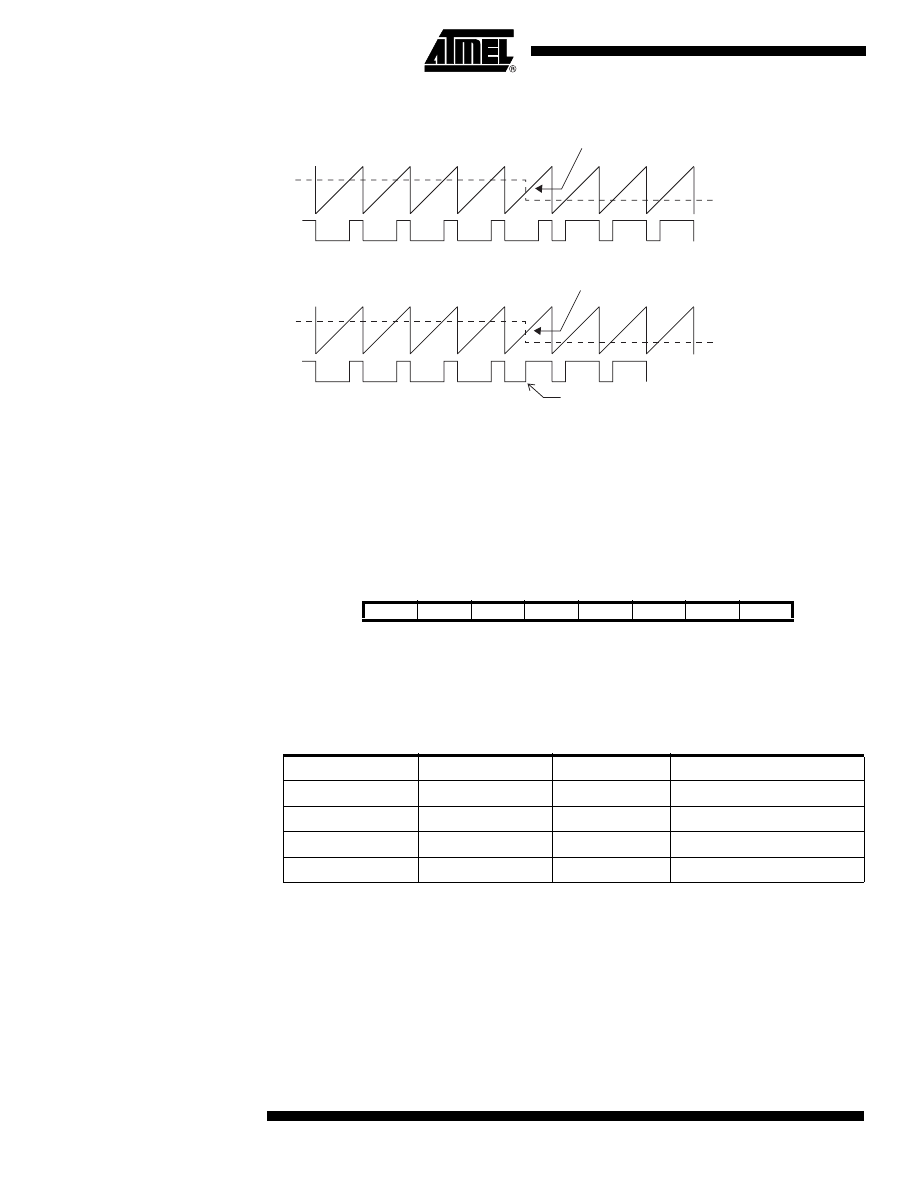
Timer/Counter1 in PWM Mode
When the PWM mode is selected, Timer/Counter1 and the Output Compare Register A
(OCR1A) form an 8-bit, free-running and glitch-free PWM with outputs on the
PB1(OC1A) pin. Timer/Counter1 acts as an up-counter, counting up from $00 up to the
value specified in the second Output Compare Register OCR1B, and starting from $00
up again. When the counter value matches the contents of the Output Compare Regis-
ter OCR1A, the PB1(OC1A) pin is set or cleared according to the settings of the
COM1A1/COM1A0 bits in the Timer/Counter1 Control Registers TCCR1. Refer to Table
12 for details.
Note that in PWM mode, writing to the Output Compare OCR1A, the data value is first
transferred to a temporary location. The value is latched into OCR1A when the
Timer/Counter reaches OCR1B. This prevents the occurrence of odd-length PWM
pulses (glitches) in the event of an unsynchronized OCR1A write. See Figure 22 for an
example.
Bit
7
6
5
4
3
2
1
0
$2E
MSB
LSB
OCR1A
Read/Write
R/W
R/W
R/W
R/W
R/W
R/W
R/W
R/W
Initial Value
0
0
0
0
0
0
0
0
Table 12. Compare Mode Select in PWM Mode
COM1A1
COM1A0
Effect on Compare Pin
0
0
Not connected
0
1
Not connected
1
0
Cleared on compare match (up-counting) (non-inverted PWM). Set
when TCNT1 = $00.
1
1
Set on compare match (up-counting) (inverted PWM). Cleared when
TCNT1 = $00.
32
ATtiny15L
1187F–AVR–06/05
Figure 22. Effects of Unsynchronized OCR Latching
During the time between the write and the latch operation, a read from OCR1A will read
the contents of the temporary location. This means that the most recently written value
always will read out of OCR1A.
When OCR1A contains $00 or the top value, as specified in OCR1B Register, the output
PB1(OC1A) is held low or high according to the settings of COM1A1/COM1A0. This is
shown in Table 13.
Timer/Counter1 Output
Compare RegisterB – OCR1B
The Output Compare Register1 (OCR1B) is an 8-bit read/write register. This register is
used in the PWM mode only, and it limits the top value to which the Timer/Counter1
keeps counting. After reaching OCR1B in PWM mode, the counter starts from $00.
In PWM mode, the Timer Overflow Flag (TOV1) is set as in normal Timer/Counter
mode. Timer Overflow Interrupt1 operates exactly as in normal Timer/Counter mode,
i.e., it is executed when TOV1 is set provided that Timer Overflow Interrupt and global
interrupts are enabled. This also applies to the Timer Output Compare A Flag and
interrupt.
PWM Output OC1A
PWM Output OC1A
Unsynchronized OC1A Latch
Synchronized OC1A Latch
Counter Value
Compare Value
Counter Value
Compare Value
Compare Value Changes
Glitch
Compare Value Changes
Bit
7
6
5
4
3
2
1
0
$2D
MSB
LSB
OCR1B
Read/Write
R/W
R/W
R/W
R/W
R/W
R/W
R/W
R/W
Initial Value
1
1
1
1
1
1
1
1
Table 13. PWM Outputs when OCR1A = $00 or OCR1B
COM1A1
COM1A0
OCR1B
Output PWMn
1
0
$00
L
1
0
OCR1B
H
1
1
$00
H
1
1
OCR1B
L

33
ATtiny15L
1187F–AVR–06/05
The frequency of the PWM will be Timer Clock Frequency divided by OCR1B value + 1.
The exact duty-cycle of the non-inverted PWM output is:
Where:
T
T1
is the period of the selected Timer/Counter1 Clock Source.
T
PCK
is the period of the PCK Clock (39.1 ns).
Table 14. Timer/Counter1 Clock Prescale Select
Clock Selection
OCR1B
PWM Frequency
CK
159
10 kHz
PCK/8
159
20 kHz
PCK/4
213
30 kHz
PCK/4
159
40 kHz
PCK/2
255
50 kHz
PCK/2
213
60 kHz
PCK/2
181
70 kHz
PCK/2
159
80 kHz
PCK/2
141
90 kHz
PCK
255
100 kHz
PCK
231
110 kHz
PCK
213
120 kHz
PCK
195
130 kHz
PCK
181
140 kHz
PCK
169
150 kHz
OCR1A +1
(
) T
T1
×
T
PCK
–
OCR1B +1
(
) T
T1
×
---------------------------------------------------------------------
34
ATtiny15L
1187F–AVR–06/05
The Watchdog Timer
The Watchdog Timer is clocked from a separate On-chip Oscillator that runs at 1 MHz.
This is the typical value at V
CC
= 5V. See “Typical Characteristics” on page 66 for typical
values at other V
CC
levels. By controlling the Watchdog Timer prescaler, the Watchdog
Reset interval can be adjusted from 16 to 2,048 ms, as shown in Table 15. The WDR
(Watchdog Reset) instruction resets the Watchdog Timer. Eight different clock cycle
periods can be selected to determine the reset period. If the reset period expires without
another Watchdog Reset, the ATtiny15L resets and executes from the Reset Vector.
For timing details on the Watchdog Reset, refer to page 17.
To prevent unintentional disabling of the Watchdog, a special turn-off sequence must be
followed when the Watchdog is disabled. Refer to the description of the Watchdog Timer
Control Register for details.
Figure 23. Watchdog Timer
The Watchdog Timer Control
Register – WDTCR
• Bits 7..5 – Res: Reserved Bits
These bits are reserved bits in the ATtiny15L and will always read as zero.
• Bit 4 – WDTOE: Watchdog Turn-off Enable
This bit must be set (one) when the WDE bit is cleared. Otherwise, the Watchdog will
not be disabled. Once set, hardware will clear this bit to zero after four clock cycles.
Refer to the description of the WDE bit for a Watchdog disable procedure.
• Bit 3 – WDE: Watchdog Enable
When the WDE is set (one), the Watchdog Timer is enabled and if the WDE is cleared
(zero), the Watchdog Timer function is disabled. WDE can be cleared only when the
WDTOE bit is set (one). To disable an enabled Watchdog Timer, the following proce-
dure must be followed:
1 MHz at Vcc = 5V
350 KHz at Vcc = 3V
WATCHDOG
PRESCALER
WATCHDOG
Oscillator
RESET
WDP0
WDP1
WDP2
WDE
MCU RESET
Bit
7
6
5
4
3
2
1
0
$21
–
–
–
WDTOE
WDE
WDP2
WDP1
WDP0
WDTCR
Read/Write
R
R
R
R/W
R/W
R/W
R/W
R/W
Initial Value
0
0
0
0
0
0
0
0

35
ATtiny15L
1187F–AVR–06/05
1.
In the same operation, write a logical “1” to WDTOE and WDE. A logical “1” must
be written to WDE even though it is set to one before the disable operation starts.
2.
Within the next four clock cycles, write a logical “0” to WDE. This disables the
Watchdog.
• Bits 2..0 – WDP2, WDP1, WDP0: Watchdog Timer Prescaler Bits 2, 1, and 0
The WDP2, WDP1 and WDP0 bits determine the Watchdog Timer prescaling when the
Watchdog Timer is enabled. The different prescaling values and their corresponding
time-out periods are shown in Table 15.
Table 15. Watchdog Timer Prescale Select
WDP2
WDP1
WDP0
Time-out Period
0
0
0
16K cycles
0
0
1
32K cycles
0
1
0
64K cycles
0
1
1
128K cycles
1
0
0
256K cycles
1
0
1
512K cycles
1
1
0
1,024K cycles
1
1
1
2,048K cycles

36
ATtiny15L
1187F–AVR–06/05
EEPROM Read/Write
Access
The EEPROM Access Registers are accessible in the I/O space.
The write access time is in the range of 4.6 - 8.2 ms, depending on the frequency of the
calibrated RC Oscillator. See Table 16 for details. A self-timing function however, lets
the user software detect when the next byte can be written. If the user code contains
code that writes the EEPROM, some precautions must be taken. In heavily filtered
power supplies, V
CC
is likely to rise or fall slowly on Power-up/down. This causes the
device for some period of time to run at a voltage lower than specified as minimum for
the clock frequency used. CPU operation under these conditions is likely to cause the
Program Counter to perform unintentional jumps and eventually execute the EEPROM
write code. To secure EEPROM integrity, the user is advised to use an external under-
voltage reset circuit in this case.
In order to prevent unintentional EEPROM writes, a two-state write procedure must be
followed. Refer to the description of the EEPROM Control Register for details of this.
When the EEPROM is read or written, the CPU is halted for two clock cycles before the
next instruction is executed.
The EEPROM Address
Register – EEAR
• Bit 7, 6 – Res: Reserved Bits
These bits are reserved bits in the ATtiny15L and will always read as zero.
• Bit 5..0 – EEAR5..0: EEPROM Address
The EEPROM Address Register (EEAR) specifies the EEPROM address in the 64 bytes
EEPROM space. The EEPROM data bytes are addresses linearly between 0 and 63.
The initial value of EEAR is undefined. A proper value must be written before the
EEPROM may be accessed.
The EEPROM Data Register –
EEDR
• Bit 7..0 – EEDR7..0: EEPROM Data
For the EEPROM write operation, the EEDR Register contains the data to be written to
the EEPROM in the address given by the EEAR Register. For the EEPROM read oper-
ation, the EEDR contains the data read out from the EEPROM at the address given by
EEAR.
Bit
7
6
5
4
3
2
1
0
$1E
–
–
EEAR5
EEAR4
EEAR3
EEAR2
EEAR1
EEAR0
EEAR
Read/Write
R
R
R/W
R/W
R/W
R/W
R/W
R/W
Initial vAlue
0
0
X
X
X
X
X
X
Bit
7
6
5
4
3
2
1
0
$1D
MSB
LSB
EEDR
Read/Write
R/W
R/W
R/W
R/W
R/W
R/W
R/W
R/W
Initial Value
0
0
0
0
0
0
0
0

37
ATtiny15L
1187F–AVR–06/05
The EEPROM Control Register
– EECR
• Bit 7..4 – RES: Reserved Bits
These bits are reserved bits in the ATtiny15L and will always read as zero.
• Bit 3 – EERIE: EEPROM Ready Interrupt Enable
When the I-bits in SREG and EERIE are set (one), the EEPROM Ready Interrupt is
enabled. When cleared (zero), the interrupt is disabled. The EEPROM Ready Interrupt
generates a constant interrupt when EEWE is cleared (zero).
• Bit 2 – EEMWE: EEPROM Master Write Enable
The EEMWE bit determines whether setting EEWE to one causes the EEPROM to be
written. When EEMWE is set (one), setting EEWE will write data to the EEPROM at the
selected address. If EEMWE is zero, setting EEWE will have no effect. When EEMWE
has been set (one) by software, hardware clears the bit to zero after four clock cycles.
See the description of the EEWE bit for an EEPROM write procedure.
• Bit 1 – EEWE: EEPROM Write Enable
The EEPROM Write Enable Signal – EEWE – is the write strobe to the EEPROM. When
address and data are correctly set up, the EEWE bit must be set to write the value in to
the EEPROM. The EEMWE bit must be set when the logical “1” is written to EEWE, oth-
erwise no EEPROM write takes place. The following procedure should be followed
when writing the EEPROM (the order of steps 2 and 3 is not essential):
1.
Wait until EEWE becomes zero.
2.
Write new EEPROM address to EEAR (optional).
3.
Write new EEPROM data to EEDR (optional).
4.
Write a logical “1” to the EEMWE bit in EECR.
5.
Within four clock cycles after setting EEMWE, write a logical “1” to EEWE.
Caution: An interrupt between step 4 and step 5 will make the write cycle fail, since the
EEPROM Master Write Enable will time-out. If an interrupt routine accessing the
EEPROM is interrupting another EEPROM access, the EEAR or EEDR Register will be
modified, causing the interrupted EEPROM access to fail. It is recommended to have
the Global Interrupt Flag cleared during the four last steps to avoid these problems.
When the write access time (typically 5.1 ms if the internal RC Oscillator is calibrated to
1.6 MHz) has elapsed, the EEWE bit is cleared (zero) by hardware. The user software
can poll this bit and wait for a zero before writing the next byte. When EEWE has been
set, the CPU is halted for two cycles before the next instruction is executed.
• Bit 0 – EERE: EEPROM Read Enable
The EEPROM Read Enable Signal EERE is the read strobe to the EEPROM. When the
correct address is set up in the EEAR Register, the EERE bit must be set. When the
EERE bit is cleared (zero) by hardware, requested data is found in the EEDR Register.
The EEPROM read access takes one instruction and there is no need to poll the EERE
bit. When EERE has been set, the CPU is halted for four cycles before the next instruc-
tion is executed.
Bit
7
6
5
4
3
2
1
0
$1C
–
–
–
–
EERIE
EEMWE
EEWE
EERE
EECR
Read/Write
R
R
R
R
R/W
R/W
R/W
R/W
Initial value
0
0
0
0
0
0
X
0

38
ATtiny15L
1187F–AVR–06/05
The user should poll the EEWE bit before starting the read operation. If a write operation
is in progress when new data or address is written to the EEPROM I/O Registers, the
write operation will be interrupted and the result is undefined.
The calibrated oscillator is used to time EEPROM. In Table 16 the typical programming
time is listed for EEPROM access from the CPU.
Preventing EEPROM
Corruption
During periods of low V
CC
,
the EEPROM data can be corrupted because the supply volt-
age is too low for the CPU and the EEPROM to operate properly. These issues are the
same as for board-level systems using the EEPROM and the same design solutions
should be applied.
An EEPROM data corruption can be caused by two situations when the voltage is too
low. First, a regular write sequence to the EEPROM requires a minimum voltage to
operate correctly. Second, the CPU itself can execute instructions incorrectly if the sup-
ply voltage for executing instructions is too low.
EEPROM data corruption can easily be avoided by following these design recommen-
dations (one is sufficient):
1.
Keep the AVR RESET active (low) during periods of insufficient power supply
voltage. This can be done by enabling the internal Brown-out Detector (BOD) if
the operating voltage matches the detection level. If not, an external low V
CC
Reset Protection circuit can be applied.
2.
Keep the AVR core in Power-down sleep mode during periods of low V
CC
. This
will prevent the CPU from attempting to decode and execute instructions, effec-
tively protecting the EEPROM Registers from unintentional writes.
3.
Store constants in Flash memory if the ability to change memory contents from
software is not required. Flash memory cannot be updated by the CPU and will
not be subject to corruption.
Table 16. Typical EEPROM Programming Times
Parameter
Number of Calibrated RC
Oscillator Cycles
Min Programming
Time
Max Programming
Time
EEPROM write
(from CPU)
8192
4.6 ms
8.2 ms
39
ATtiny15L
1187F–AVR–06/05
The Analog
Comparator
The Analog Comparator compares the input values on the positive pin PB0 (AIN0) and
negative pin PB1 (AIN1). When the voltage on the positive pin PB0 (AIN0) is higher than
the voltage on the negative pin PB1 (AIN1), the Analog Comparator Output (ACO) is set
(one). The comparator’s output can trigger a separate interrupt, exclusive to the Analog
Comparator. The user can select interrupt triggering on comparator output rise, fall or
toggle. A block diagram of the Comparator and its surrounding logic is shown in Figure
24.
Figure 24. Analog Comparator Block Diagram
The Analog Comparator
Control and Status Register –
ACSR
• Bit 7 – ACD: Analog Comparator Disable
When this bit is set (one), the power to the Analog Comparator is switched off. This bit
can be set at any time to turn off the Analog Comparator. This will reduce power con-
sumption in Active and Idle mode. When changing the ACD-bit, the Analog Comparator
Interrupt must be disabled by clearing the ACIE bit in ACSR. Otherwise an interrupt can
occur when the bit is changed.
• Bit 6 – ACBG: Analog Comparator Bandgap Select
When this bit is set, a fixed bandgap voltage of 1.22 ± 0.05V replaces the normal input
to the positive pin (AIN0) of the comparator. When this bit is cleared, the normal input
pin PB0 is applied to the positive pin of the comparator.
• Bit 5 – ACO: Analog Comparator Output
ACO is directly connected to the comparator output.
• Bit 4 – ACI: Analog Comparator Interrupt Flag
This bit is set (one) when a comparator output event triggers the interrupt mode defined
by ACI1 and ACI0. The Analog Comparator Interrupt routine is executed if the ACIE bit
is set (one) and the I-bit in SREG is set (one). ACI is cleared by hardware when execut-
ing the corresponding interrupt handling vector. Alternatively, ACI is cleared by writing a
logical “1” to the flag.
Bit
7
6
5
4
3
2
1
0
$08
ACD
ACBG
ACO
ACI
ACIE
–
ACIS1
ACIS0
ACSR
Read/Write
R/W
R/W
R
R/W
R/W
R
R/W
R/W
Initial Value
0
0
X
0
0
0
0
0

40
ATtiny15L
1187F–AVR–06/05
• Bit 3 – ACIE: Analog Comparator Interrupt Enable
When the ACIE bit is set (one) and the I-bit in the Status Register is set (one), the Ana-
log Comparator Interrupt is activated. When cleared (zero), the interrupt is disabled.
• Bit 2 – Res: Reserved Bit
This bit is a reserved bit in the ATtiny15L and will always read as zero.
• Bits 1, 0 – ACIS1, ACIS0: Analog Comparator Interrupt Mode Select
These bits determine the comparator events that trigger the Analog Comparator Inter-
rupt. The different settings are shown in Table 17.
Note:
1. When changing the ACIS1/ACIS0 bits, The Analog Comparator Interrupt must be dis-
abled by clearing its Interrupt Enable bit in the ACSR Register. Otherwise an interrupt
can occur when the bits are changed.
Table 17. ACIS1/ACIS0 Settings
ACIS1
ACIS0
Interrupt Mode
0
0
Comparator Interrupt on Output Toggle
0
1
Reserved
1
0
Comparator Interrupt on Falling Output Edge
1
1
Comparator Interrupt on Rising Output Edge

41
ATtiny15L
1187F–AVR–06/05
The Analog-to-Digital
Converter, Analog
Multiplexer, and Gain
Stages
Features
•
10-bit Resolution
•
±2 LSB Absolute Accuracy
•
0.5 LSB Integral Non-linearity
•
Optional Offset Cancellation
•
65 - 260 µs Conversion Time
•
Up to 15 kSPS
•
4 Multiplexed Single-ended Input Channels
•
1 Differential Input Channel with Optional Gain of 20x
•
2.56V Internal Voltage Reference
•
0 - 2.56V Differential Input Voltage Range
•
0 - V
CC
Single-ended Input Voltage Range
•
Optional Left Adjustment for ADC Result Readout
•
Free Running or Single Conversion Mode
•
Interrupt on ADC Conversion Complete
•
Sleep Mode Noise Canceler
The ATtiny15L features a 10-bit successive approximation ADC. The ADC is connected
to a 4-channel Analog Multiplexer that allows one differential voltage input and four sin-
gle-ended voltage inputs constructed from the pins of Port B. The differential input (PB3,
PB4) is equipped with a programmable gain stage, providing amplification step of 26 dB
(20x) on the differential input voltage before the A/D conversion. The single-ended volt-
age inputs at PB2..PB5 refer to 0V (GND).
The ADC contains a Sample and Hold Amplifier that ensures that the input voltage to
the ADC is held at a constant level during conversion. A block diagram of the ADC is
shown in Figure 25.
An internal reference voltage of nominally 2.56V is provided On-chip and this reference
can optionally be externally decoupled at the AREF (PB0) pin by a capacitor for better
noise performance. Alternatively, V
CC
can be used as reference voltage for single-
ended channels. There is also an option to use an external voltage reference and turn
off the internal voltage reference. These options are selected using the REFS1..0 bits of
the ADMUX Control Register.
42
ATtiny15L
1187F–AVR–06/05
Figure 25. Analog-to-Digital Converter Block Schematic
Operation
The ADC converts an analog input voltage to a 10-bit digital value through successive
approximation. The minimum value represents GND and the maximum value represents
the selected reference voltage minus 1 LSB.
The voltage reference for the ADC may be selected by writing to the REFS1..0 bits in
ADMUX. V
CC
, the AREF pin, or an internal 2.56V reference may be selected as the ADC
voltage reference. Optionally, the 2.56V internal voltage reference may be decoupled by
an external capacitor at the AREF pin to improve noise immunity.
The analog input channel and differential gain are selected by writing to the MUX2..0
bits in ADMUX. Any of the four ADC input pins ADC3..0 can be selected as single-
ended inputs to the ADC. ADC2 and ADC3 can be selected as positive and negative
input, respectively, to the differential gain amplifier.
If differential channels are selected, the differential gain stage amplifies the voltage dif-
ference between the selected input pair by the selected gain factor, 1x or 20x, according
to the setting of the MUX2..0 bits in ADMUX. This amplified value then becomes the
analog input to the ADC. If single-ended channels are used, the gain amplifier is
bypassed altogether.
If ADC2 is selected as both the positive and negative input to the differential gain ampli-
fier (ADC2 - ADC2), the remaining offset in the gain stage and conversion circuitry can
be measured directly as the result of the conversion. This figure can be subtracted from
subsequent conversions with the same gain setting to reduce offset error to below 1
LSB.
The ADC can operate in two modes – Single Conversion and Free Running. In Single
Conversion mode, each conversion will have to be initiated by the user. In Free Running
ADC CONVERSION
COMPLETE IRQ
8-BIT DATA BUS
9
0
ADC MULTIPLEXER
SELECT (ADMUX)
ADC CTRL. & STATUS
REGISTER (ADCSR)
ADC DATA REGISTER
(ADCH/ADCL)
MUX2
ADIE
ADFR
ADSC
ADEN
ADIF
ADIF
MUX1
MUX0
ADPS0
ADPS1
ADPS2
CONVERSION LOGIC
10-BIT DAC
+
-
SAMPLE & HOLD
COMPARATOR
INTERNAL
2.56 V
REFERENCE
MUX DECODER
VCC
AREF
ADC3
ADC2
ADC1
ADC0
REFS0
REFS1
ADLAR
+
-
CHANNEL SELECTION
GAIN SELECTION
ADC[9:0]
GAIN
AMPLIFIER
PRESCALER
SINGLE ENDED / DIFFERENTIAL SELECTION
POS.
INPUT
MUX
NEG.
INPUT
MUX
43
ATtiny15L
1187F–AVR–06/05
mode, the ADC is constantly sampling and updating the ADC Data Register. The ADFR
bit in ADCSR selects between the two available modes.
The ADC is enabled by setting the ADC Enable bit, ADEN in ADCSR. Voltage reference
and input channel selections will not go into effect until ADEN is set. The ADC does not
consume power when ADEN is cleared, so it is recommended to switch off the ADC
before entering Power-saving sleep modes.
A conversion is started by writing a logical “1” to the ADC Start Conversion bit, ADSC.
This bit stays high as long as the conversion is in progress and will be set to zero by
hardware when the conversion is completed. If a different data channel is selected while
a conversion is in progress, the ADC will finish the current conversion before performing
the channel change.
The ADC generates a 10-bit result, which is presented in the ADC Data Registers,
ADCH and ADCL. By default, the result is presented right-adjusted, but can optionally
be presented left-adjusted by setting the ADLAR bit in ADMUX.
If the result is left-adjusted and no more than 8-bit precision is required, it is sufficient to
read ADCH. Otherwise, ADCL must be read first, then ADCH, to ensure that the content
of the Data Registers belongs to the same conversion. Once ADCL is read, ADC access
to data registers is blocked. This means that if ADCL has been read, and a conversion
completes before ADCH is read, neither register is updated and the result from the con-
version is lost. When ADCH is read, ADC access to the ADCH and ADCL Registers is
re-enabled.
The ADC has its own interrupt, which can be triggered when a conversion completes.
When ADC access to the Data Registers is prohibited between reading of ADCH and
ADCL, the interrupt will trigger even if the result is lost.
Prescaling and
Conversion Timing
Figure 26. ADC Prescaler
The successive approximation circuitry requires an input clock frequency between
50 kHz and 200 kHz. Using a higher input frequency will affect the conversion accuracy,
see “ADC Characteristics” on page 50. The ADC module contains a prescaler, which
divides the system clock to an acceptable ADC clock frequency.
The ADPSn bits in ADCSR are used to generate a proper ADC clock input frequency
from any CK frequency above 100 kHz. The prescaler starts counting from the moment
7-BIT ADC PRESCALER
ADC CLOCK SOURCE
CK
ADPS0
ADPS1
ADPS2
CK/128
CK/2
CK/4
CK/8
CK/16
CK/32
CK/64
Reset
ADEN
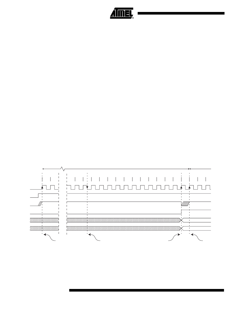
44
ATtiny15L
1187F–AVR–06/05
the ADC is switched on by setting the ADEN bit in ADCSR. The prescaler keeps running
for as long as the ADEN bit is set, and is continuously reset when ADEN is low.
When initiating a conversion by setting the ADSC bit in ADCSR, the conversion starts at
the following rising edge of the ADC clock cycle. If differential channels are selected, the
conversion will only start at every other rising edge of the ADC clock cycle after ADEN
was set.
A normal conversion takes 13 ADC clock cycles. In certain situations, the ADC needs
more clock cycles to perform initialization and minimize offset errors. These extended
conversions take 25 ADC clock cycles and occur as the first conversion after one of the
following events:
•
The ADC is switched on (ADEN in ADCSR is set).
•
The voltage reference source is changed (the REFS1..0 bits in ADMUX change
value).
•
A differential channel is selected (MUX2 in ADMUX is “1”). Note that subsequent
conversions on the same channel are not extended conversions.
The actual sample-and-hold takes place 1.5 ADC clock cycles after the start of a normal
conversion and 13.5 ADC clock cycles after the start of an extended conversion. When
a conversion is complete, the result is written to the ADC Data Registers, and ADIF is
set. In Single Conversion mode, ADSC is cleared simultaneously. The software may
then set ADSC again, and a new conversion will be initiated on the first rising ADC clock
edge. In Free Running mode, a new conversion will be started immediately after the
conversion completes while ADSC remains high. Using Free Running mode and an
ADC clock frequency of 200 kHz gives the lowest conversion time, 65
µs
, equivalent to
15 kSPS. For a summary of conversion times, see Table 18.
Figure 27. ADC Timing Diagram, First Conversion (Single Conversion Mode)
Sign and MSB of Result
LSB of Result
ADC Clock
ADSC
Sample & Hold
ADIF
ADCH
ADCL
Cycle Number
ADEN
1
2
12
13
14
15
16
17
18
19
20
21
22
23
24
25
1
2
Extended Conversion
Next
Conversion
3
MUX and REFS
Update
MUX and REFS
Update
Conversion
Complete
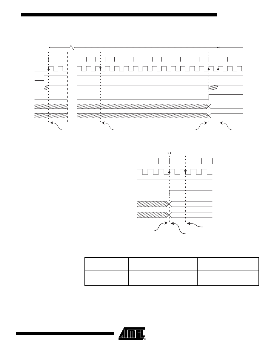
45
ATtiny15L
1187F–AVR–06/05
Figure 28. ADC Timing Diagram, Single Conversion
Figure 29. ADC Timing Diagram, Free Running Conversion
Sign and MSB of Result
LSB of Result
ADC Clock
ADSC
Sample & Hold
ADIF
ADCH
ADCL
Cycle Number
ADEN
1
2
12
13
14
15
16
17
18
19
20
21
22
23
24
25
1
2
Extended Conversion
Next
Conversion
3
MUX and REFS
Update
MUX and REFS
Update
Conversion
Complete
Table 18. ADC Conversion Time
Condition
Sample & Hold
(Cycles from Start of Conversion)
Conversion
Time (Cycles)
Conversion
Time (µs)
Extended Conversion
13.5
25.0
125 - 500
Normal Conversions
1.5
13.0
65 - 260
11
12
13
Sign and MSB of Result
LSB of Result
ADC Clock
ADSC
ADIF
ADCH
ADCL
Cycle Number
1
2
One Conversion
Next Conversion
3
4
Conversion
Complete
Sample & Hold
MUX and REFS
Update

46
ATtiny15L
1187F–AVR–06/05
ADC Noise Canceler
Function
The ADC features a noise canceler that enables conversion during ADC Noise Reduc-
tion mode (see “Sleep Modes” on page 23) to reduce noise induced from the CPU core
and other I/O peripherals. If other I/O peripherals must be active during conversion, this
mode works equivalently for Idle mode. To make use of this feature, the following proce-
dure should be used:
1.
Make sure that the ADC is enabled and is not busy converting. Single Conver-
sion mode must be selected and the ADC conversion complete interrupt must be
enabled.
ADEN = 1
ADSC = 0
ADFR = 0
ADIE = 1
2.
Enter ADC Noise Reduction mode (or Idle mode). The ADC will start a conver-
sion once the CPU has been halted.
3.
If no other interrupts occur before the ADC conversion completes, the ADC inter-
rupt will wake up the MCU and execute the ADC conversion complete interrupt
routine.
The ADC Multiplexer Selection
Register – ADMUX
• Bits 7..6 – REFS1..REFS0: Reference Selection Bits
These bits select the voltage reference for the ADC, as shown in Table 19. If these bits
are changed during a conversion, the change will not go into effect until this conversion
is complete (ADIF in ADCSR is set). Whenever these bits are changed, the next
conversion will take 25 ADC clock cycles. If active channels are used, using AVCC or an
external AREF higher than (AVCC - 1V) is not recommended, as this will affect ADC
accuracy. The internal voltage reference options may not be used if an external
reference voltage is being applied to the AREF pin.
• Bit 5 – ADLAR: ADC Left Adjust Result
The ADLAR bit affects the presentation of the ADC conversion result in the ADC Data
Register. If ADLAR is cleared, the result is right-adjusted. If ADLAR is set, the result is
left-adjusted. Changing the ADLAR bit will affect the ADC Data Register immediately,
regardless of any ongoing conversions. For a complete description of this bit, see “The
ADC Data Register – ADCL and ADCH” on page 49.
Bit
7
6
5
4
3
2
1
0
$07
REFS1
REFS0
ADLAR
–
–
MUX2
MUX1
MUX0
ADMUX
Read/Write
R/W
R/W
R/W
R
R
R/W
R/W
R/W
Initial Value
0
0
0
0
0
0
0
0
Table 19. Voltage Reference Selections for ADC
REFS1
REFS0
Voltage Reference Selection
0
0
V
CC
used as analog reference, disconnected from PB0 (AREF).
0
1
External Voltage Reference at PB0 (AREF) pin, Internal Voltage
Reference turned off.
1
0
Internal Voltage Reference without external bypass capacitor,
disconnected from PB0 (AREF).
1
1
Internal Voltage Reference with external bypass capacitor at PB0 (AREF)
pin.
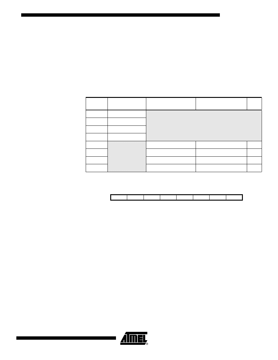
47
ATtiny15L
1187F–AVR–06/05
• Bits 4..3 – Res: Reserved Bits
These bits are reserved bits in the ATtiny15L and always read as zero.
• Bits 2..0 – MUX2..MUX0: Analog Channel and Gain Selection Bits 2..0
The value of these bits selects which analog input is connected to the ADC. In case of
differential input (PB3 - PB4), gain selection is also made with these bits. Selecting PB3
as both inputs to the differential gain stage enables offset measurements. Refer to Table
20 for details. If these bits are changed during a conversion, the change will not go into
effect until this conversion is complete (ADIF in ADCSR is set).
Note:
1. For offset calibration only. See “Operation” on page 42.
The ADC Control and Status
Register – ADCSR
• Bit 7 – ADEN: ADC Enable
Writing a logical “1” to this bit enables the ADC. By clearing this bit to zero, the ADC is
turned off. Turning the ADC off while a conversion is in progress will terminate this
conversion.
• Bit 6 – ADSC: ADC Start Conversion
In Single Conversion mode, a logical “1” must be written to this bit to start each conver-
sion. In Free Running mode, a logical “1” must be written to this bit to start the first
conversion.
When the conversion completes, ADSC returns to zero in Single Conversion mode and
stays high in Free Running mode.
Writing a “0” to this bit has no effect.
• Bit 5 – ADFR: ADC Free Running Select
When this bit is set (one), the ADC operates in Free Running mode. In this mode, the
ADC samples and updates the Data Registers continuously. Clearing this bit (zero) will
terminate Free Running mode. If active channels are used (MUX2 in ADMUX set), the
Table 20. Input Channel and Gain Selections
MUX2..0
Single-ended
Input
Positive
Differential Input
Negative
Differential Input
Gain
000
ADC0 (PB5)
N/A
001
ADC1 (PB2)
010
ADC2 (PB3)
011
ADC3 (PB4)
100
N/A
ADC2 (PB3)
ADC2 (PB3)
1x
101
ADC2 (PB3)
ADC2 (PB3)
20x
110
ADC2 (PB3)
ADC3 (PB4)
1x
111
ADC2 (PB3)
ADC3 (PB4)
20x
Bit
7
6
5
4
3
2
1
0
$06
ADEN
ADSC
ADFR
ADIF
ADIE
ADPS2
ADPS1
ADPS0
ADCSR
Read/Write
R/W
R/W
R/W
R/W
R/W
R/W
R/W
R/W
Initial Value
0
0
0
0
0
0
0
0

48
ATtiny15L
1187F–AVR–06/05
channel must be selected before entering Free Running mode. Selecting an active
channel after entering Free Running mode may result in undefined operation from the
ADC.
• Bit 4 – ADIF: ADC Interrupt Flag
This bit is set (one) when an ADC conversion completes and the Data Registers are
updated. The ADC Conversion Complete Interrupt is executed if the ADIE bit and the I-
bit in SREG are set (one). ADIF is cleared by hardware when executing the correspond-
ing interrupt handling vector. Alternatively, ADIF is cleared by writing a logical “1” to the
flag. Beware that if doing a read-modify-write on ADCSR, a pending interrupt can be dis-
abled. This also applies if the SBI and CBI instructions are used.
• Bit 3 – ADIE: ADC Interrupt Enable
When this bit is set (one) and the I-bit in SREG is set (one), the ADC Conversion Com-
plete Interrupt is activated.
• Bits 2..0 – ADPS2..ADPS0: ADC Prescaler Select Bits
These bits determine the division factor between the CK frequency and the input clock
to the ADC. See Table 21.
Table 21. ADC Prescaler Selections
ADPS2
ADPS1
ADPS0
Division Factor
0
0
0
2
0
0
1
2
0
1
0
4
0
1
1
8
1
0
0
16
1
0
1
32
1
1
0
64
1
1
1
128

49
ATtiny15L
1187F–AVR–06/05
The ADC Data Register –
ADCL and ADCH
ADLAR = 0
ADLAR = 1
When an ADC conversion is complete, the result is found in these two registers. When
ADCL is read, the ADC Data Register is not updated until ADCH is read. If the result is
left adjusted and no more than 8-bit precision is required, it is sufficient to read ADCH.
Otherwise, ADCL must be read first, then ADCH. The ADLAR bit in ADMUX affects the
way the result is read from the registers. If ADLAR is set, the result is left-adjusted. If
ADLAR is cleared (default), the result is right-adjusted.
• ADC9..0: ADC Conversion Result
These bits represent the result from the conversion. For the differential channel, this is
the value after gain adjustment, as indicated in Table 20 on page 47. For single-ended
conversion, or if ADLAR or SIGN is zero, $000 represents ground and $3FF represents
the selected reference voltage minus one LSB.
Scanning Multiple Channels
Since change of analog channel always is delayed until a conversion is finished, the
Free Running mode can be used to scan multiple channels without interrupting the con-
verter. Typically, the ADC Conversion Complete Interrupt will be used to perform the
channel shift. However, the user should take the following fact into consideration:
The interrupt triggers once the result is ready to be read. In Free Running mode, the
next conversion will start immediately when the interrupt triggers. If ADMUX is
changed after the interrupt triggers, the next conversion has already started, and the
old setting is used.
Bit
15
14
13
12
11
10
9
8
$05
–
–
–
–
–
–
ADC9
ADC8
ADCH
$04
ADC7
ADC6
ADC5
ADC4
ADC3
ADC2
ADC1
ADC0
ADCL
7
6
5
4
3
2
1
0
Read/Write
R
R
R
R
R
R
R
R
R
R
R
R
R
R
R
R
Initial Value
0
0
0
0
0
0
0
0
0
0
0
0
0
0
0
0
Bit
15
14
13
12
11
10
9
8
$05
ADC9
ADC8
ADC7
ADC6
ADC5
ADC4
ADC3
ADC2
ADCH
$04
ADC1
ADC0
–
–
–
–
–
–
ADCL
7
6
5
4
3
2
1
0
Read/Write
R
R
R
R
R
R
R
R
R
R
R
R
R
R
R
R
Initial Value
0
0
0
0
0
0
0
0
0
0
0
0
0
0
0
0

50
ATtiny15L
1187F–AVR–06/05
ADC Noise-canceling
Techniques
Digital circuitry inside and outside the ATtiny15L generates EMI, which might affect the
accuracy of analog measurements. If conversion accuracy is critical, the noise level can
be reduced by applying the following techniques:
1.
The analog part of the ATtiny15L and all analog components in the application
should have a separate analog ground plane on the PCB. This ground plane is
connected to the digital ground plane via a single point on the PCB.
2.
Keep analog signal paths as short as possible. Make sure analog tracks run over
the analog ground plane, and keep them well away from high-speed switching
digital tracks.
3.
Use the ADC noise canceler function to reduce induced noise from the CPU.
4.
If some Port B pins are used as digital outputs, it is essential that these do not
switch while a conversion is in progress.
ADC Characteristics
Symbol
Parameter
Condition
Min
Typ
Max
Units
Resolution
Single-ended Conversion
10.0
Bits
Differential Conversion
Gain = 1x or 20x
8.0
Bits
Absolute Accuracy
Single-ended Conversion
V
REF
= 4V
ADC Clock = 200 kHz
1.0
2.0
LSB
Single-ended Conversion
V
REF
= 4V
ADC Clock = 1 MHz
4.0
LSB
Single-ended Conversion
V
REF
= 4V
ADC Clock = 2 MHz
16.0
LSB
Integral Non-linearity
V
REF
> 2V
0.5
LSB
Differential Non-linearity
V
REF
> 2V
0.5
LSB
Zero Error (Offset)
V
REF
> 2V
1.0
LSB
Conversion Time
Free Running Conversion
65.0
260.0
µs
Clock Frequency
50.0
200.0
kHz
V
REF
Reference Voltage
Single-ended Conversion
2.0
V
CC
V
Differential Conversion
2.0
V
CC
- 0.2
V
V
INT
Internal Voltage Reference
2.4
2.56
2.7
V
R
REF
Reference Input Resistance
6.0
10.0
13.0
k
Ω
R
AIN
Analog Input Resistance
100.0
M
Ω

51
ATtiny15L
1187F–AVR–06/05
I/O Port B
All AVR ports have true read-modify-write functionality when used as general digital I/O
ports. This means that the direction of one port pin can be changed without unintention-
ally changing the direction of any other pin with the SBI and CBI instructions. The same
applies for changing drive value (if configured as output) or enabling/disabling of pull-up
resistors (if configured as input).
Port B is a 6-bit bi-directional I/O port.
Three data memory address locations are allocated for Port B, one each for the Data
Register – PORTB, $18, Data Direction Register – DDRB, $17, and the Port B Input
Pins – PINB, $16. The Port B Input Pins address is read-only, while the Data Register
and the Data Direction Register are read/write.
Ports PB5..0 have special functions as described in the section “Pin Descriptions” on
page 4. If PB5 is not configured as External Reset, it is input with no pull-up or as an
open-drain output. All I/O pins have individually selectable pull-ups, which can be over-
ridden with pull-up disable.
The Port B output buffers on PB0 to PB4 can sink 20 mA and thus drive LED displays
directly. PB5 can sink 12 mA. When pins PB0 to PB4 are used as inputs and are exter-
nally pulled low, they will source current (I
IL
) if the internal pull-ups are activated.
Unconnected Pins
If some pins are unused, it is recommended to ensure that these pins have a defined
level. The simplest method to ensure a defined level of an unused pin, is to enable the
internal pull-up. In this case, the pull-up will be disabled during reset. If low power con-
sumption during reset is important, it is recommended to use an external pull-up or pull-
down. Connecting unused pins directly to Vcc or GND is not recommended, since this
may cause excessive currents if the pin is accidentally configured as an output.
Alternative Functions of
Port B
In ATtiny15L four Port B pins – PB2, PB3, PB4, and PB5 – have alternative functions as
inputs for the ADC. If some Port B pins are configured as outputs, it is essential that
these do not switch when a conversion is in progress. This might corrupt the result of the
conversion. During Power-down mode and ADC Noise Reduction mode, the Schmitt
triggers of the digital inputs are disconnected on these pins. This allows an analog input
voltage close to V
CC
/2 to be present during Power-down without causing excessive
power consumption. The Port B pins with alternate functions are shown in Table 1 on
page 4.
When the pins PB4..0 are used for the alternate function, the DDRB and PORTB Regis-
ters have to be set according to the alternate function description. When PB5 is used as
External Reset pin, the values in the corresponding DDRB and PORTB bit are ignored.
The Port B Data Register –
PORTB
The Port B Data Direction
Register – DDRB
Bit
7
6
5
4
3
2
1
0
$18
–
–
–
PORTB4
PORTB3
PORTB2
PORTB1
PORTB0
PORTB
Read/Write
R
R
R
R/W
R/WS
R/W
R/W
R/W
Initial Value
0
0
0
0
0
0
0
0
Bit
7
6
5
4
3
2
1
0
$17
–
–
DDB5
DDB4
DDB3
DDB2
DDB1
DDB0
DDRB
Read/Write
R
R
R/W
R/W
R/W
R/W
R/W
R/W
Initial Value
0
0
0
0
0
0
0
0

52
ATtiny15L
1187F–AVR–06/05
The Port B Input Pins Address
– PINB
The Port B Input Pins address (PINB) is not a register, and this address enables access
to the physical value on each Port B pin. When reading PORTB, the PORTB Data Latch
is read, and when reading PINB, the logical values present on the pins are read.
PORT B as General Digital I/O
The lower five pins in Port B are equal when used as digital I/O pins.
PBn, general I/O pin: The DDBn bit in the DDRB Register selects the direction of this
pin. If DDBn is set (one), PBn is configured as an output pin. If DDBn is cleared (zero),
PBn is configured as an input pin. If PORTBn is set (one) when the pin is configured as
an input pin, the MOS pull-up resistor is activated. To switch the pull-up resistor off, the
PORTBn has to be cleared (zero) or the pin has to be configured as an output pin. Pull-
ups for all ports can be disabled also by setting PUD-bit in the MCUCR Register.
Note:
1. n: 4, 3…0, pin number.
On ATtiny15L, PB5 is input or open-drain output. Because this pin is used for 12V pro-
gramming, there is no ESD protection diode limiting the voltage on the pin to
V
CC
+ 0.5V. Thus, special care should be taken to ensure that the voltage on this pin
does not rise above V
CC
+ 1V during normal operation. This may cause the MCU to
reset or enter Programming mode unintentionally.
All Port B pins are connected to a pin change detector that can trigger the pin change
interrupt. See “Pin Change Interrupt” on page 22 for details.
Alternate Functions of Port B
The alternate pin functions of Port B are:
• RESET – PORT B, Bit 5
When the RSTDISBL Fuse is unprogrammed, this pin serves as External Reset. When
the RSTDISBL Fuse is programmed, this pin is a general input pin or a open-drain out-
put pin. If DDB5 is cleared (zero), PB5 is configured as an input pin. If DDB5 is set
(one), the pin is a open-drain output.
• SCK/INT0/T0 – PORT B, Bit 2
In Serial Programming mode, this pin serves as the serial clock input, SCK.
In Normal mode, this pin can serve as the external interrupt0 input. See the interrupt
description for details on how to enable this interrupt. Note that activity on this pin will
trigger the interrupt even if the pin is configured as an output.
Bit
7
6
5
4
3
2
1
0
$16
–
–
PINB5
PINB4
PINB3
PINB2
PINB1
PINB0
PINB
Read/Write
R
R
R
R
R
R
R
R
Initial Value
0
0
N/A
N/A
N/A
N/A
N/A
N/A
Table 22. DDBn Effects on Port B Pins
DDBn
PORTBn
I/O
Pull-up
Comment
0
0
Input
No
Tri-state (High-Z)
0
1
Input
No
PUD bit in the MCUCR Register is set.
0
1
Input
Yes
PBn will source current if ext. pulled low.
PUD bit in the MCUCR Register is cleared.
1
0
Output
No
Push-pull Zero Output
1
1
Output
No
Push-pull One Output

53
ATtiny15L
1187F–AVR–06/05
In Normal mode, this pin can serve as the external counter clock input. See the
Timer/Counter0 description for further details. If external Timer/Counter clocking is
selected, activity on this pin will clock the counter even if it is configured as an output.
• MISO/OC1A/AIN1 – PORT B, Bit 1
In Serial Programming mode, this pin serves as the serial data output, MISO.
In Normal mode, this pin can serve as Timer/Counter1 output compare match output
(OC1A). See the Timer/Counter1 description for further details, and how to enable the
output. The OC1A pin is also the output pin for PWM mode timer function.
This pin also serves as the negative input of the On-chip Analog Comparator.
• MOSI/AIN0/AREF – PORT B, Bit 0
In Serial Programming mode, this pin serves as the serial data input, MOSI.
In Normal mode, this pin also serves as the positive input of the On-chip Analog
Comparator.
In ATtiny15L, this pin can be chosen to be the reference voltage for the ADC. Refer to
the section “The Analog-to-Digital Converter, Analog Multiplexer, and Gain Stages” for
details.

54
ATtiny15L
1187F–AVR–06/05
Memory
Programming
Program and Data
Memory Lock Bits
The ATtiny15L MCU provides two Lock bits that can be left unprogrammed, “1”, or can
be programmed, “0”, to obtain the additional features listed in Table 23. The Lock bits
can only be erased with the Chip Erase command
.
Fuse Bits
The ATtiny15L has six Fuse bits (BODLEVEL, BODEN, SPIEN, RSTDSBL, and
CKSEL1..0). All the Fuse bits are programmable in both High-voltage and Low-voltage
Serial Programming modes. Changing the Fuses does not have effect while in program-
ming mode.
•
The BODLEVEL Fuse selects the Brown-out Detection level and changes the start-
up times. See “Brown-out Detection” on page 17. See Table 5 on page 15. Default
value is programmed “0”.
•
When the BODEN Fuse is programed “0”, the Brown-out Detector is enabled. See
“Brown-out Detection” on page 17. Default value is unprogrammed “1”.
•
When the SPIEN Fuse bit is programmed “0”, Low-voltage Serial Program and Data
Downloading is enabled. Default value is programmed “0”. Unprogramming this fuse
while in the Low-voltage Serial Programming mode will disable future In-System
downloading attempts.
•
When the RSTDISBL Fuse is programmed “0”, the External Reset function of pin
PB5 is disabled
. Default value is unprogrammed “1”. Programming this fuse while
in the Low-voltage Serial Programming mode will disable future In-System
downloading attempts.
•
CKSEL1..0 Fuses: See Table 5 on page 15 for which combination of CKSEL1..0 to
use. Default value is “00”, 64 ms + 18 CK.
The status of the Fuse bits is not affected by Chip Erase.
Note:
1. If the RSTDISBL Fuse is programmed, then the programming hardware should apply
+12V to PB5 while the ATtiny15L is in Power-on Reset. If not, the part can fail to enter
Programming mode caused by drive contention on PB0 and/or PB5.
Signature Bytes
All Atmel microcontrollers have a three-byte signature code that identifies the device.
The three bytes reside in a separate address space, and for the ATtiny15L they are:
1.
$000 : $1E (indicates manufactured by Atmel).
2.
$001 : $90 (indicates 1 Kb Flash memory).
3.
$002 : $06 (indicates ATtiny15L device when $001 is $90).
Table 23. Lock Bit Protection Modes
Memory Lock Bits
Protection Type
Mode
LB1
LB2
1
1
1
No memory lock features enabled.
2
0
1
Further programming of the Flash and EEPROM is disabled.
3
0
0
Same as mode 2, but verify is also disabled.
55
ATtiny15L
1187F–AVR–06/05
Calibration Byte
The ATtiny15L has a one-byte calibration value for the internal RC Oscillator. This byte
resides in the high byte of address $000 in the signature address space. To make use of
this byte, it should be read from this location and written into the normal Flash Program
memory. At start-up, the user software must read this Flash location and write the value
to the OSCCAL Register.
Programming the Flash
Atmel’s ATtiny15L offers 1K byte of In-System Reprogrammable Flash Program mem-
ory and 64 bytes of in-System Reprogrammable EEPROM Data memory.
The ATtiny15L is shipped with the On-chip Flash program and EEPROM data memory
arrays in the erased state (i.e., contents = $FF) and ready to be programmed.
This device supports a High-voltage (12V) Serial Programming mode and a Low-voltage
Serial Programming mode. The +12V is used for programming enable only, and no cur-
rent of significance is drawn by this pin (less than 100
µA)
. The Low-voltage Serial
Programming mode provides a convenient way to download program and data into the
ATtiny15L inside the user’s system.
The Program and Data memory arrays in the ATtiny15L are programmed byte-by-byte
in either Programming mode. For the EEPROM, an auto-erase cycle is provided within
the self-timed write instruction in the Low-voltage Serial Programming mode.
During programming, the supply voltage must be in accordance with Table 24.
High-voltage Serial
Programming
This section describes how to program and verify Flash Program memory, EEPROM
Data memory, Lock bits and Fuse bits in the ATtiny15L.
Figure 30. High-voltage Serial Programming
Table 24. Supply Voltage during Programming
Part
Low-voltage Serial Programming
High-voltage Serial Programming
ATtiny15L
2.7 - 5.5V
4.5 - 5.5V
PB5 (RESET)
PB3
GND
VCC
PB2
PB1
PB0
SERIAL DATA OUTPUT
SERIAL INSTR. INPUT
SERIAL DATA INPUT
SERIAL CLOCK INPUT
11.5 - 12.5V
4.5 - 5.5V
ATtiny15/L
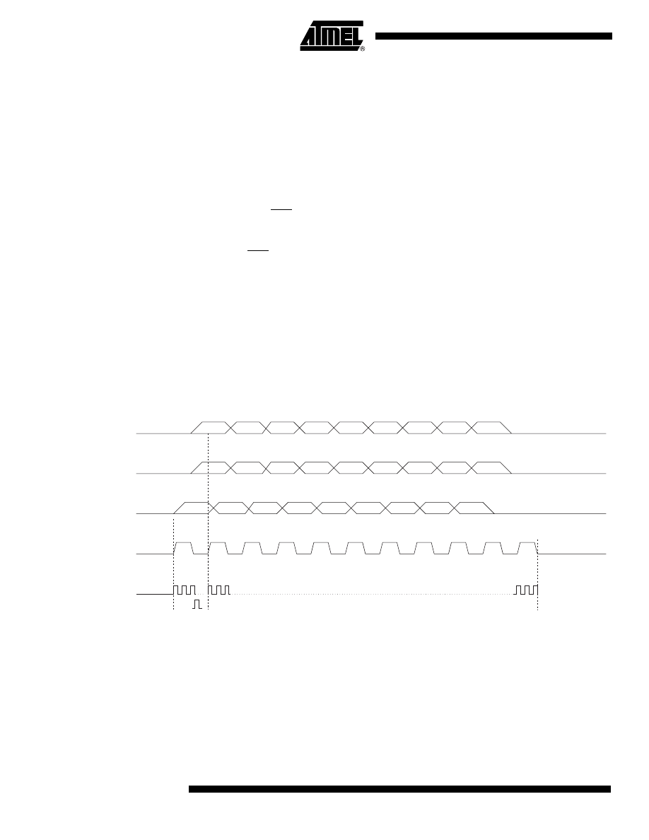
56
ATtiny15L
1187F–AVR–06/05
High-voltage Serial
Programming Algorithm
To program and verify the ATtiny15L in the High-voltage Serial Programming mode, the
following sequence is recommended (See instruction formats in Table 25):
1.
Power-up sequence:
Apply 4.5 - 5.5V between V
CC
and GND. Set PB5 and PB0 to “0” and wait at least
30 µs.
Set PB3 to “0”. Wait at least 100 ns.
Apply 12V to PB5 and wait at least 100 ns before changing PB0. Wait 8 µs
before giving any instructions.
2.
The Flash array is programmed one byte at a time by supplying first the address,
then the low and high data byte. The write instruction is self-timed; wait until the
PB2 (RDY/BSY) pin goes high.
3.
The EEPROM array is programmed one byte at a time by supplying first the
address, then the data byte. The write instruction is self-timed; wait until the PB2
(RDY/BSY) pin goes high.
4.
Any memory location can be verified by using the Read instruction, which
returns the contents at the selected address at serial output PB2.
5.
Power-off sequence:
Set PB3 to “0”.
Set PB5 to “0”.
Turn V
CC
power off.
When writing or reading serial data to the ATtiny15L, data is clocked on the eigth rising
edge of the 16 external clock pulses needed to generate the internal clock. See Figure
31, Figure 32, and Table 26 for an explanation.
Figure 31. High-voltage Serial Programming Waveforms
MSB
MSB
MSB
LSB
LSB
LSB
0
1
2
3
4
5
6
7
8
9
10
SERIAL DATA INPUT
PB0
SERIAL INSTR. INPUT
PB1
SERIAL DATA OUTPUT
PB2
INTERNAL CK
SERIAL CLOCK INPUT
PB3
16x

57
ATtiny15L
1187F–AVR–06/05
Table 25. High-voltage Serial Programming Instruction Set for ATtiny15L
Instruction
Instruction Format
Operation Remarks
Instr.1
Instr.2
Instr.3
Instr.4
Chip Erase
PB0
PB1
PB2
0_1000_0000_00
0_0100_1100_00
x_xxxx_xxxx_xx
0_0000_0000_00
0_0110_0100_00
x_xxxx_xxxx_xx
0_0000_0000_00
0_0110_1100_00
x_xxxx_xxxx_xx
0_0000_0000_00
0_0100_1100_00
x_xxxx_xxxx_xx
Wait after Instr.3 until PB2
goes high for the Chip Erase
cycle to finish.
Write Flash
High and Low
Address
PB0
PB1
PB2
0_0001_0000_00
0_0100_1100_00
x_xxxx_xxxx_xx
0_0000_000a_00
0_0001_1100_00
x_xxxx_xxxx_xx
0_bbbb_bbbb_00
0_0000_1100_00
x_xxxx_xxxx_xx
Repeat Instr.2 for a new 256
byte page. Repeat Instr.3 for
each new address.
Write Flash
Low Byte
PB0
PB1
PB2
0_ i i i i_i i i i _00
0_0010_1100_00
x_xxxx_xxxx_xx
0_0000_0000_00
0_0110_0100_00
x_xxxx_xxxx_xx
0_0000_0000_00
0_0110_1100_00
0_0000_0000_00
Wait after Instr.3 until PB2
goes high. Repeat Instr.1,
Instr. 2 and Instr.3 for each
new address.
Write Flash
High Byte
PB0
PB1
PB2
0_ i i i i_i i i i _00
0_0011_1100_00
x_xxxx_xxxx_xx
0_0000_0000_00
0_0111_0100_00
x_xxxx_xxxx_xx
0_0000_0000_00
0_0111_1100_00
0_0000_0000_00
Wait after Instr.3 until PB2
goes high. Repeat Instr.1,
Instr. 2 and Instr.3 for each
new address.
Read Flash
High and Low
Address
PB0
PB1
PB2
0_0000_0010_00
0_0100_1100_00
x_xxxx_xxxx_xx
0_0000_000a_00
0_0001_1100_00
x_xxxx_xxxx_xx
0_bbbb_bbbb_00
0_0000_1100_00
x_xxxx_xxxx_xx
Repeat Instr.2 and Instr.3 for
each new address.
Read Flash
Low Byte
PB0
PB1
PB2
0_0000_0000_00
0_0110_1000_00
x_xxxx_xxxx_xx
0_0000_0000_00
0_0110_1100_00
o_oooo_ooox_xx
Repeat Instr.1 and Instr.2 for
each new address.
Read Flash
High Byte
PB0
PB1
PB2
0_0000_0000_00
0_0111_1000_00
x_xxxx_xxxx_xx
0_0000_0000_00
0_0110_1100_00
o_oooo_ooox_xx
Repeat Instr.1 and Instr.2 for
each new address.
Write
EEPROM
Low Address
PB0
PB1
PB2
0_0001_0001_00
0_0100_1100_00
x_xxxx_xxxx_xx
0_00bb_bbbb_00
0_0000_1100_00
x_xxxx_xxxx_xx
Repeat Instr.2 for each new
address.
Write
EEPROM
Byte
PB0
PB1
PB2
0_ i i i i_i i i i _00
0_0010_1100_00
x_xxxx_xxxx_xx
0_0000_0000_00
0_0110_0100_00
x_xxxx_xxxx_xx
0_0000_0000_00
0_0110_1100_00
0_0000_0000_00
Wait after Instr.3 until PB2
goes high
Read
EEPROM
Low Address
PB0
PB1
PB2
0_0000_0011_00
0_0100_1100_00
x_xxxx_xxxx_xx
0_00bb_bbbb_00
0_0000_1100_00
x_xxxx_xxxx_xx
Repeat Instr.2 for each new
address.
Read
EEPROM
Byte
PB0
PB1
PB2
0_0000_0000_00
0_0110_1000_00
x_xxxx_xxxx_xx
0_0000_0000_00
0_0110_1100_00
o_oooo_ooox_xx
Repeat Instr.2 for each new
address
Write Fuse
Bits
PB0
PB1
PB2
0_0100_0000_00
0_0100_1100_00
x_xxxx_xxxx_xx
0_8765_1143_00
0_0010_1100_00
x_xxxx_xxxx_xx
0_0000_0000_00
0_0110_0100_00
x_xxxx_xxxx_xx
0_0000_0000_00
0_0110_1100_00
x_xxxx_xxxx_xx
Wait after Instr.4 until PB2
goes high. Write 8 - 3 = “0” to
program the Fuse bit.
Write Lock
Bits
PB0
PB1
PB2
0_0010_0000_00
0_0100_1100_00
x_xxxx_xxxx_xx
0_0000_0210_00
0_0010_1100_00
x_xxxx_xxxx_xx
0_0000_0000_00
0_0110_0100_00
x_xxxx_xxxx_xx
0_0000_0000_00
0_0110_1100_00
0_0000_0000_00
Wait after Instr.4 until PB2
goes high. Write 2, 1 = “0” to
program the Lock bit.
Read Fuse
Bits
PB0
PB1
PB2
0_0000_0100_00
0_0100_1100_00
x_xxxx_xxxx_xx
0_0000_0000_00
0_0110_1000_00
x_xxxx_xxxx_xx
0_0000_0000_00
0_0110_1100_00
8_765x_x43x_xx
Reading 8 - 3 = “0” means the
Fuse bit is programmed.

58
ATtiny15L
1187F–AVR–06/05
Note:
1. a = address high bits
b = address low bits
i = data in
o = data out
x = don’t care
1 = Lock Bit1
2 = Lock Bit2
3 = CKSEL0 Fuse
4 = CKSEL1 Fuse
5 = RSTDSBL Fuse
6 = SPIEN Fuse
7 = BODEN Fuse
8 = BODLEVEL Fuse
The Lock bits can only be cleared by executing a Chip Erase.
Read Lock
Bits
PB0
PB1
PB2
0_0000_0100_00
0_0100_1100_00
x_xxxx_xxxx_xx
0_0000_0000_00
0_0111_1000_00
x_xxxx_xxxx_xx
0_0000_0000_00
0_0111_1100_00
x_xxxx_21xx_xx
Reading 2, 1 = “0” means the
Lock bit is programmed
Read
Signature
Bytes
PB0
PB1
PB2
0_0000_1000_00
0_0100_1100_00
x_xxxx_xxxx_xx
0_0000_00bb_00
0_0000_1100_00
x_xxxx_xxxx_xx
0_0000_0000_00
0_0110_1000_00
x_xxxx_xxxx_xx
0_0000_0000_00
0_0110_1100_00
o_oooo_ooox_xx
Repeat Instr.2 - Instr.4 for
each signature byte address
Read
Calibration
Byte
PB0
PB1
PB2
0_0000_1000_00
0_0100_1100_00
x_xxxx_xxxx_xx
0_0000_0000_00
0_0000_1100_00
x_xxxx_xxxx_xx
0_0000_0000_00
0_0111_1000_00
x_xxxx_xxxx_xx
0_0000_0000_00
0_0111_1100_00
o_oooo_ooox_xx
Table 25. High-voltage Serial Programming Instruction Set for ATtiny15L
(1)
(Continued)
Instruction
Instruction Format
Operation Remarks
Instr.1
Instr.2
Instr.3
Instr.4
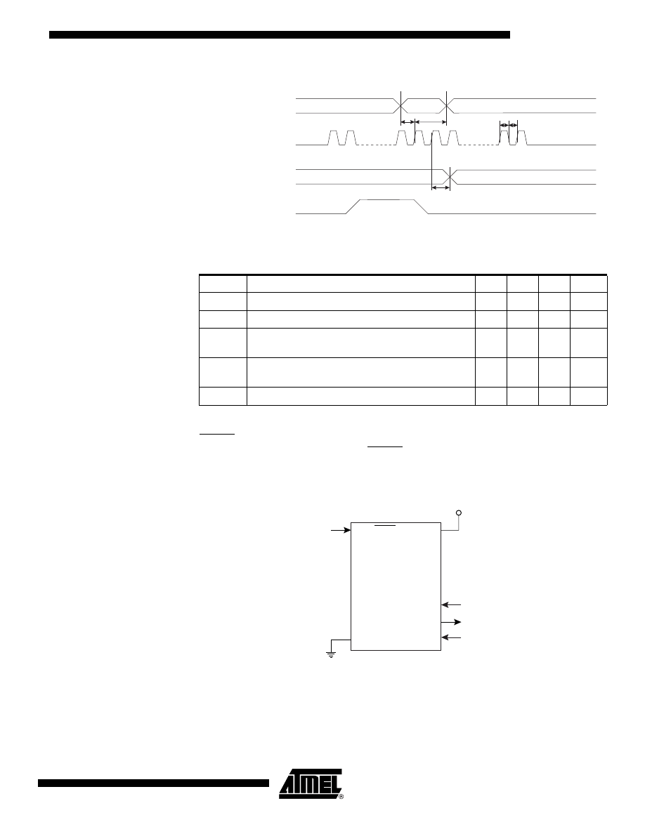
59
ATtiny15L
1187F–AVR–06/05
High-voltage Serial
Programming
Characteristics
Figure 32. High-voltage Serial Programming Timing
Low-voltage Serial
Downloading
Both the program and data memory arrays can be programmed using the SPI bus while
RESET is pulled to GND. The serial interface consists of pins SCK, MOSI (input) and
MISO (output). See Figure 33. After RESET is set low, the Programming Enable instruc-
tion needs to be executed first before program/erase instructions can be executed.
Figure 33. Serial Programming and Verify
For the EEPROM, an auto-erase cycle is provided within the self-timed write instruction
and there is no need to first execute the Chip Erase instruction. The Chip Erase instruc-
tion turns the content of every memory location in both the program and EEPROM
arrays into $FF.
The program and EEPROM memory arrays have separate address spaces: $0000 to
$01FF for Program memory and $000 to $03F for EEPROM memory.
Table 26. High-voltage Serial Programming Characteristics, T
A
= 25
°C ± 10%,
V
CC
= 5.0V ± 10% (unless otherwise noted)
Symbol
Parameter
Min
Typ
Max
Units
t
SHSL
SCI (PB3) Pulse Width High
25.0
ns
t
SLSH
SCI (PB3) Pulse Width Low
25.0
ns
t
IVSH
SDI (PB0), SII (PB1) Valid to SCI (PB3) High (8th
edge)
50.0
ns
t
SHIX
SDI (PB0), SII (PB1) Hold after SCI (PB3) High (8th
edge)
50.0
ns
t
SHOV
SCI (PB3) High (9th edge) to SDO (PB2) Valid
10.0
16.0
32.0
ns
SDI (PB0), SII (PB1)
SDO (PB2)
SCI (PB3)
t
IVSH
t
SHSL
t
SLSH
t
SHIX
t
SHOV
Internal CK
1 2 7 8 9 10 15 16
VALID
PB5 (RESET)
GND
VCC
PB2
PB1
PB0
SCK
MISO
MOSI
2.7 - 5.5V
ATtiny15/L

60
ATtiny15L
1187F–AVR–06/05
The device is clocked from the internal clock at the uncalibrated minimum frequency
(0.8 - 1.6 MHz). The minimum low and high periods for the serial clock (SCK) input are
defined as follows:
Low: > 2 MCU clock cycles
High: > 2 MCU clock cycles
Low-voltage Serial
Programming Algorithm
When writing serial data to the ATtiny15L, data is clocked on the rising edge of SCK.
When reading data from the ATtiny15L, data is clocked on the falling edge of SCK. See
Figure 34, Figure 35, and Table 28 for timing details. To program and verify the
ATtiny15L in the Serial Programming mode, the following sequence is recommended
(See 4-byte instruction formats in Table 27):
1.
Power-up sequence:
Apply power between V
CC
and GND while RESET and SCK are set to “0”. If the pro-
grammer cannot guarantee that SCK is held low during Power-up, RESET must be
given a positive pulse of at least two MCU cycles duration after SCK has been set to
“0”.
2.
Wait for at least 20 ms and enable serial programming by sending the Program-
ming Enable serial instruction to the MOSI (PB0) pin. Refer to the above section
for minimum low and high periods for the serial clock input SCK.
3.
The serial programming instructions will not work if the communication is out of
synchronization. When in sync, the second byte ($53) will echo back when issu-
ing the third byte of the Programming Enable instruction. Whether the echo is
correct or not, all four bytes of the instruction must be transmitted. If the $53 did
not echo back, give SCK a positive pulse and issue a new Programming Enable
instruction. If the $53 is not seen within 32 attempts, there is no functional device
connected.
4.
If a Chip Erase is performed (must be done to erase the Flash), wait t
WD_ERASE
after the instruction, give RESET a positive pulse, and start over from step 2.
See Table 29 on page 63 for t
WD_ERASE
value.
5.
The Flash or EEPROM array is programmed one byte at a time by supplying the
address and data together with the appropriate write instruction. An EEPROM
memory location is first automatically erased before new data is written. Use
data polling to detect when the next byte in the Flash or EEPROM can be written.
If polling is not used, wait t
WD_PROG_FL
or t
WD_PROG_EE
, respectively, before trans-
mitting the next instruction. See Table 30 on page 63 for the t
WD_PROG_FL
and
t
WD_PROG_EE
values. In an erased device, no $FFs in the data file(s) need to be
programmed.
6.
Any memory location can be verified by using the Read instruction, which
returns the content at the selected address at the serial output MISO (PB1) pin.
7.
At the end of the programming session, RESET can be set high to commence
normal operation.
8.
Power-off sequence (if needed):
Set RESET to “1”.
Turn V
CC
power off.

61
ATtiny15L
1187F–AVR–06/05
Data Polling
When a byte is being programmed into the Flash or EEPROM, reading the address
location being programmed will give the value $FF. At the time the device is ready for a
new byte, the programmed value will read correctly. This is used to determine when the
next byte can be written. This will not work for the value $FF so when programming this
value, the user will have to wait for at least t
WD_PROG_FL
before programming the next
Flash byte, or t
WD_PROG_EE
before the next EEPROM byte. As a chip-erased device con-
tains $FF in all locations, programming of addresses that are meant to contain $FF can
be skipped. This does not apply if the EEPROM is reprogrammed without chip-erasing
the device. In that case, data polling cannot be used for the value $FF and the user will
have to wait at least t
WD_PROG_EE
before programming the next byte. See Table 30 for
t
WD_PROG_FL
and t
WD_PROG_EE
values.
Figure 34. Low-voltage Serial Programming Waveforms
MSB
MSB
LSB
LSB
SERIAL CLOCK INPUT
PB2(SCK)
SERIAL DATA INPUT
PB0(MOSI)
SERIAL DATA OUTPUT
PB1(MISO)

62
ATtiny15L
1187F–AVR–06/05
Note:
1. a = address high bits
b = address low bits
H = 0 – low byte, 1 – high byte
o = data out
i = data in
x = don’t care
1 = Lock bit 1
2 = Lock bit 2
3 = CKSEL0 Fuse
4 = CKSEL1 Fuse
5 = RSTDISBL Fuse
6 = SPIEN Fuse
7 = BODEN Fuse
8 = BODLEVEL Fuse
Table 27. Low-voltage Serial Programming Instruction Set
Instruction
Instruction Format
Operation
Byte 1
Byte 2
Byte 3
Byte4
Programming Enable
1010 1100
0101 0011
xxxx xxxx
xxxx xxxx
Enable Serial Programming while
RESET is low.
Chip Erase
1010 1100
100x xxxx
xxxx xxxx
xxxx xxxx
Chip Erase Flash and EEPROM
memory arrays.
Read Program Memory
0010 H000
xxxx xxxa
bbbb bbbb
oooo oooo
Read H (high or low) data o from
program memory at word address
a:b.
Write Program Memory
0100 H000
xxxx xxxa
bbbb bbbb
iiii iiii
Write H (high or low) data i to
Program memory at word address
a:b.
Read EEPROM
Memory
1010 0000
xxxx xxxx
xxbb bbbb
oooo oooo
Read data o from EEPROM memory
at address b.
Write EEPROM
Memory
1100 0000
xxxx xxxx
xxbb bbbb
iiii iiii
Write data i to EEPROM memory at
address b.
Write Lock Bits
1010 1100
1111 1211
xxxx xxxx
xxxx xxxx
Write Lock bits. Set bits 1,2 = “0” to
program Lock bits.
Read Lock Bits
0101 1000
xxxx xxxx
xxxx xxxx
xxxx x21x
Read Lock bits. “0” = programmed,
“1” = unprogrammed.
Read Signature Bytes
0011 0000
xxxx xxxx
0000 00bb
oooo oooo
Read signature byte o at address b.
Write Fuse Bits
1010 1100
101x xxxx
xxxx xxxx
8765 1143
Set bits 8 - 3 = “0” to program, “1” to
unprogram.
Read Fuse Bits
0101 0000
xxxx xxxx
xxxx xxxx
8765 xx43
Read Fuse bits. “0” = programmed,
“1” = unprogrammed.
Read Calibration Byte
0011 1000
xxxx xxxx
0000 0000
oooo oooo
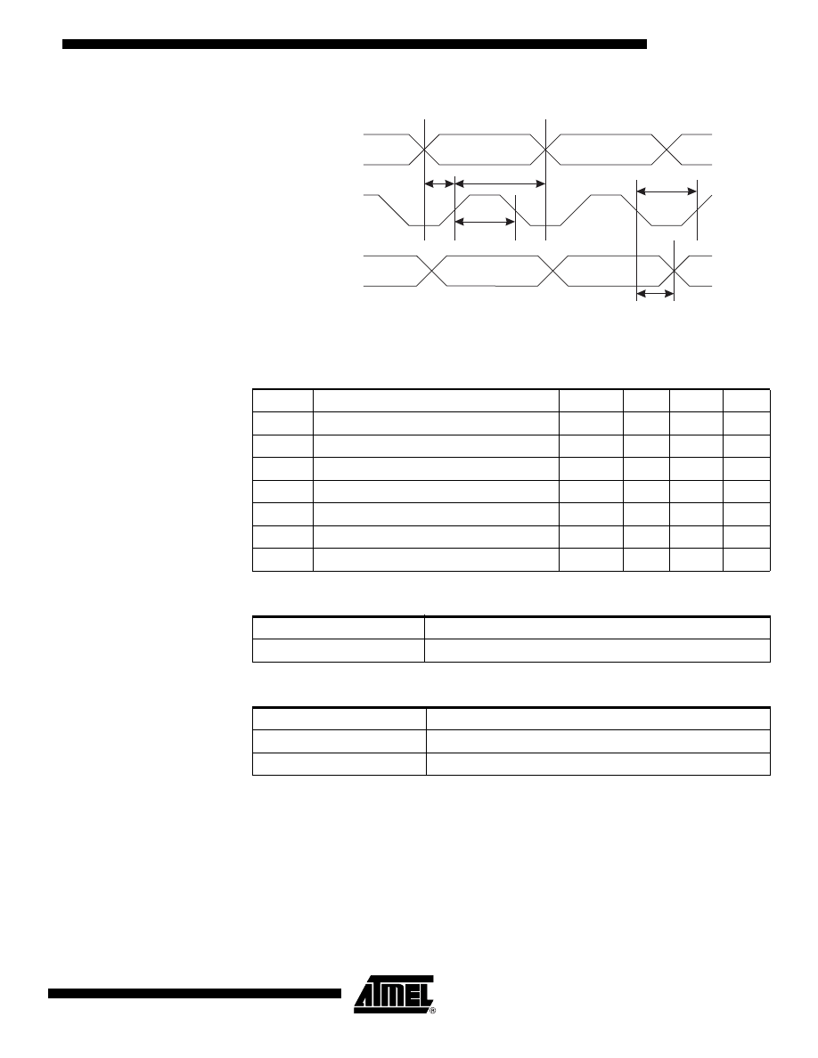
63
ATtiny15L
1187F–AVR–06/05
Low-voltage Serial
Programming
Characteristics
Figure 35. Low-voltage Serial Programming Timing
Table 28. Low-voltage Serial Programming Characteristics, T
A
= -40
°C to 85°C,
V
CC
= 2.7 - 5.5V (Unless Otherwise Noted)
Symbol
Parameter
Min
Typ
Max
Units
1/t
CLCL
RC Oscillator Frequency (V
CC
= 2.7 - 5.5V)
0.8
1.6
MHz
t
CLCL
RC Oscillator Period (V
CC
= 2.7 - 5.5V)
625.0
1250.0
ns
t
SHSL
SCK Pulse Width High
2.0 t
CLCL
ns
t
SLSH
SCK Pulse Width Low
2.0 t
CLCL
ns
t
OVSH
MOSI Setup to SCK High
t
CLCL
ns
t
SHOX
MOSI Hold after SCK High
2.0 t
CLCL
ns
t
SLIV
SCK Low to MISO Valid
10.0
16.0
32.0
ns
Table 29. Minimum Wait Delay after the Chip Erase Instruction
Symbol
Minimum Wait Delay
t
WD_ERASE
8.2 ms
Table 30. Minimum Wait Delay after Writing a Flash or EEPROM Location
Symbol
Minimum Wait Delay
t
WD_FLASH
4.1 ms
t
WD_EEPROM
8.2 ms
MOSI
MISO
SCK
t
OVSH
t
SHSL
t
SLSH
t
SHOX
t
SLIV
64
ATtiny15L
1187F–AVR–06/05
Electrical Characteristics
Absolute Maximum Ratings
Operating Temperature.................................. -55
°C to +125°C
*NOTICE:
Stresses beyond those listed under “Absolute
Maximum Ratings” may cause permanent dam-
age to the device. This is a stress rating only and
functional operation of the device at these or
other conditions beyond those indicated in the
operational sections of this specification is not
implied. Exposure to absolute maximum rating
conditions for extended periods may affect device
reliability.
Storage Temperature ..................................... -65°C to +150°C
Voltage on Any Pin Except RESET
with Respect to Ground ............................. -1.0V to V
CC
+ 0.5V
Voltage on RESET with Respect to Ground ....-1.0V to +13.0V
Maximum Operating Voltage ............................................ 6.0V
DC Current per I/O Pin ............................................... 40.0 mA
DC Current
V
CC
and GND Pins................................ 100.0 mA
DC Characteristics
T
A
= -40
°C to 85°C, V
CC
= 2.7V to 5.5V
Symbol
Parameter
Condition
Min
Typ
Max
Units
V
IL
Input Low Voltage
Except (XTAL)
-0.5
0.3 V
V
V
IL1
Input Low Voltage
XTAL
-0.5
0.1 V
V
V
IH
Input High Voltage
Except (XTAL, RESET)
0.6 V
CC
V
CC
+ 0.5
V
V
IH1
Input High Voltage
XTAL
0.7 V
CC
V
CC
+ 0.5
V
V
IH2
Input High Voltage
RESET
0.85 V
CC
V
CC
+ 0.5
V
V
OL
Output Low Voltage
Port B
I
OL
= 20 mA, V
CC
= 5V
I
OL
= 10 mA, V
CC
= 3V
0.6
0.5
V
V
V
OL
Output Low Voltage
PB5
I
OL
= 12 mA, V
CC
= 5V
I
OL
= 6 mA, V
CC
= 3V
0.6
0.5
V
V
V
OH
Output High Voltage
Port B
I
OH
= -3 mA, V
CC
= 5V
I
OH
= -1.5 mA, V
CC
= 3V
4.3
2.3
V
V
I
IL
Input Leakage Current
I/O Pin
V
CC
= 5.5V, Pin Low
(absolute value)
8.0
µA
I
IH
Input Leakage Current
I/O Pin
V
CC
= 5.5V, Pin High
(absolute value)
8.0
µA
R
I/O
I/O Pin Pull-up
35.0
122
k
Ω
I
CC
Power Supply Current
Active, V
CC
= 3V
3.0
mA
Idle, V
CC
= 3V
1.0
1.2
mA
Power-down
, V
CC
= 3V
WDT enabled
9.0
15.0
µA
Power-down
, V
CC
= 3V
WDT disabled
<1.0
2.0
µA

65
ATtiny15L
1187F–AVR–06/05
Note:
1. “Max” means the highest value where the pin is guaranteed to be read as low.
2. “Min” means the lowest value where the pin is guaranteed to be read as high.
3. Although each I/O port can sink more than the test conditions (20 mA at V
CC
= 5V, 10 mA at V
CC
= 3V) under steady state
conditions (non-transient), the following must be observed:
1] The sum of all I
OL
, for all ports, should not exceed 100 mA.
If I
OL
exceeds the test condition, V
OL
may exceed the related specification.
Pins are not guaranteed to sink current greater than the listed test conditions.
4. Although each I/O port can source more than the test conditions (3 mA at V
CC
= 5V, 1.5 mA at V
CC
= 3V) under steady state
conditions (non-transient), the following must be observed:
1] The sum of all I
OH
, for all ports, should not exceed 100 mA.
If I
OH
exceeds the test condition, V
OH
may exceed the related specification. Pins are not guaranteed to source current
greater than the listed test condition.
5. Minimum V
CC
for Power-down is 1.5V (only with BOD disabled).
V
ACIO
Analog Comparator
Input Offset Voltage
V
CC
= 5V
V
IN
= V
CC
/2
40.0
mV
I
ACLK
Analog Comparator
Input Leakage Current
V
CC
= 5V
V
IN
= V
CC
/2
-50.0
50.0
nA
T
ACID
Analog Comparator
Initialization Delay
V
CC
= 2.7V
V
CC
= 4.0V
750.0
500.0
ns
DC Characteristics (Continued)
T
A
= -40
°C to 85°C, V
CC
= 2.7V to 5.5V
Symbol
Parameter
Condition
Min
Typ
Max
Units

66
ATtiny15L
1187F–AVR–06/05
Typical
Characteristics
The following charts show typical behavior. These data are characterized but not tested.
All current consumption measurements are performed with all I/O pins configured as
inputs and with internal pull-ups enabled.
The current consumption is a function of several factors such as: Operating voltage,
operating frequency, loading of I/O pins, switching rate of I/O pins, code executed and
ambient temperature. The dominating factors are operating voltage and frequency.
The current drawn from capacitive loaded pins may be estimated (for one pin) as
C
L
•V
CC
•f where C
L
= load capacitance, V
CC
= operating voltage and f = average switch-
ing frequency of I/O pin.
The difference between current consumption in Power-down mode with Watchdog
Timer enabled and Power-down mode with Watchdog Timer disabled represents the dif-
ferential current drawn by the Watchdog Timer.
Figure 36. Active Supply Current vs. V
CC
0
0.5
1
1.5
2
2.5
3
3.5
4
4.5
2.5
3
3.5
4
4.5
5
5.5
6
ACTIVE SUPPLY CURRENT vs. V
cc
DEVICE CLOCKED BY 1.6MHz INTERNAL RC OSCILLATOR
I
cc
(mA)
V
cc
(V)
T = 85
˚
C
A
T = 25
˚
C
A
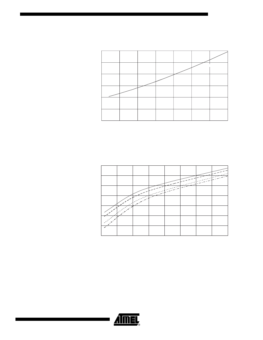
67
ATtiny15L
1187F–AVR–06/05
Figure 37. Idle Supply Current vs. V
CC
Figure 38. Calibrated Internal RC Oscillator Frequency vs. V
CC
0
0.5
1
1.5
2
2.5
3
2.5
3
3.5
4
4.5
5
5.5
6
IDLE SUPPLY CURRENT vs. V
cc
DEVICE CLOCKED BY 1.6MHz INTERNAL RC OSCILLATOR
I
cc
(mA)
V
cc
(V)
T = 85
˚
C
A
T = 25
˚
C
A
0.88
0.90
0.92
0.94
0.96
0.98
1.00
1.02
2
2.5
3
3.5
4
4.5
5
5.5
6
25˚C
Operating Voltage (V)
Relative Calibrated RC Oscillator Frequency vs. Operating Voltage
T = 25
˚
C
A
T = 85
˚
C
A
T = 45
˚
C
A
T = 70
˚
C
A
F
requency Relativ
e to Nominal F
requency at 25˚C and
V
CC
= 5.0V
Note: The nominal calibrated RC oscillator frequency is 1.6 MHz.
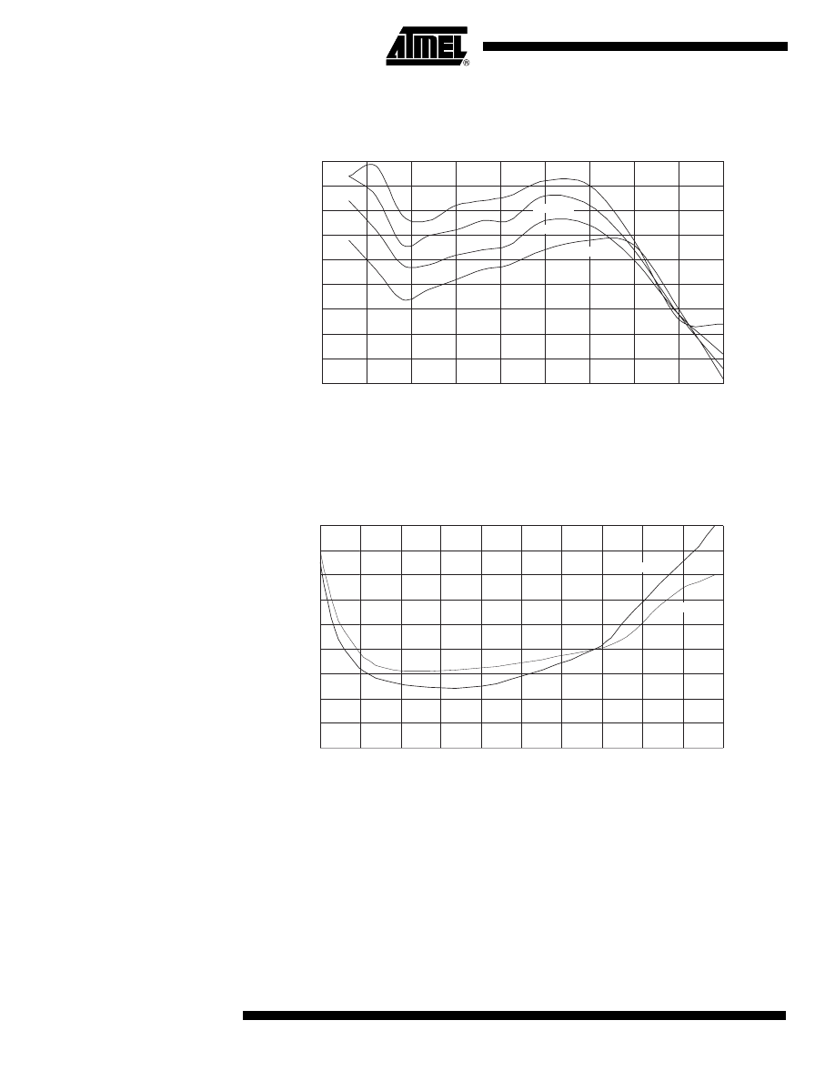
68
ATtiny15L
1187F–AVR–06/05
Figure 39. Bandgap Voltage vs. V
CC
Figure 40. Analog Comparator Offset Voltage vs. Common Mode Voltage
Note:
1. Analog Comparator offset voltage is measured as absolute offset.
BANDGAP VOLTAGE vs. V
cc
MEASURED WITH ANALOG COMPARATOR
V
BG
(V)
V
cc
(V)
1.292
1.293
1.294
1.295
1.296
1.297
1.298
1.299
1.3
1.301
1.5
2
2.5
3
3.5
4
4.5
5
5.5
6
T = 85
˚
C
A
T = 25
˚
C
A
T = 45
˚
C
A
T = 70
˚
C
A
0
2
4
6
8
10
12
14
16
18
0
0.5
1
1.5
2
2.5
3
3.5
4
4.5
5
ANALOG COMPARATOR OFFSET VOLTAGE vs.
V = 5V
cc
COMMON MODE VOLTAGE
Common Mode Voltage (V)
Offset Voltage (mV)
T = 85
˚
C
A
T = 25
˚
C
A
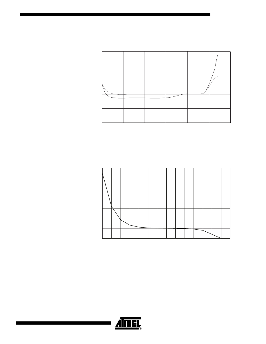
69
ATtiny15L
1187F–AVR–06/05
Figure 41. Analog Comparator Offset Voltage vs. Common Mode Voltage
Figure 42. Analog Comparator Input Leakage Current
0
2
4
6
8
10
0
0.5
1
1.5
2
2.5
3
ANALOG COMPARATOR OFFSET VOLTAGE vs.
COMMON MODE VOLTAGE
Common Mode Voltage (V)
Offset Voltage (mV)
V = 2.7V
cc
T = 85
˚
C
A
T = 25
˚
C
A
60
50
40
30
20
10
0
-10
0
0.5
1.5
1
2
2.5
3.5
3
4
4.5
5
6
6.5
7
5.5
ANALOG COMPARATOR INPUT LEAKAGE CURRENT
T = 25
˚
C
A
I
(nA)
A
CLK
V (V)
IN
V = 6V
CC

70
ATtiny15L
1187F–AVR–06/05
Figure 43. Watchdog Oscillator Frequency vs. V
CC
Note:
1. Sink and source capabilities of I/O ports are measured on one pin at a time.
Figure 44. Pull-up Resistor Current vs. Input Voltage
0
200
400
600
800
1000
1200
1400
1600
1,5
2
2,5
3
3,5
4
4,5
5
5,5
6
T = 85
˚
C
A
T = 25
˚
C
A
WATCHDOG OSCILLATOR FREQUENCY vs. V
cc
V (V)
cc
F
(KHz)
RC
0
20
40
60
80
100
120
0
0.5
1
1.5
2
2.5
3
3.5
4
4.5
5
PULL-UP RESISTOR CURRENT vs. INPUT VOLTAGE
V = 5V
cc
I (
µ
A)
OP
V (V)
OP
T = 85
˚
C
A
T = 25
˚
C
A
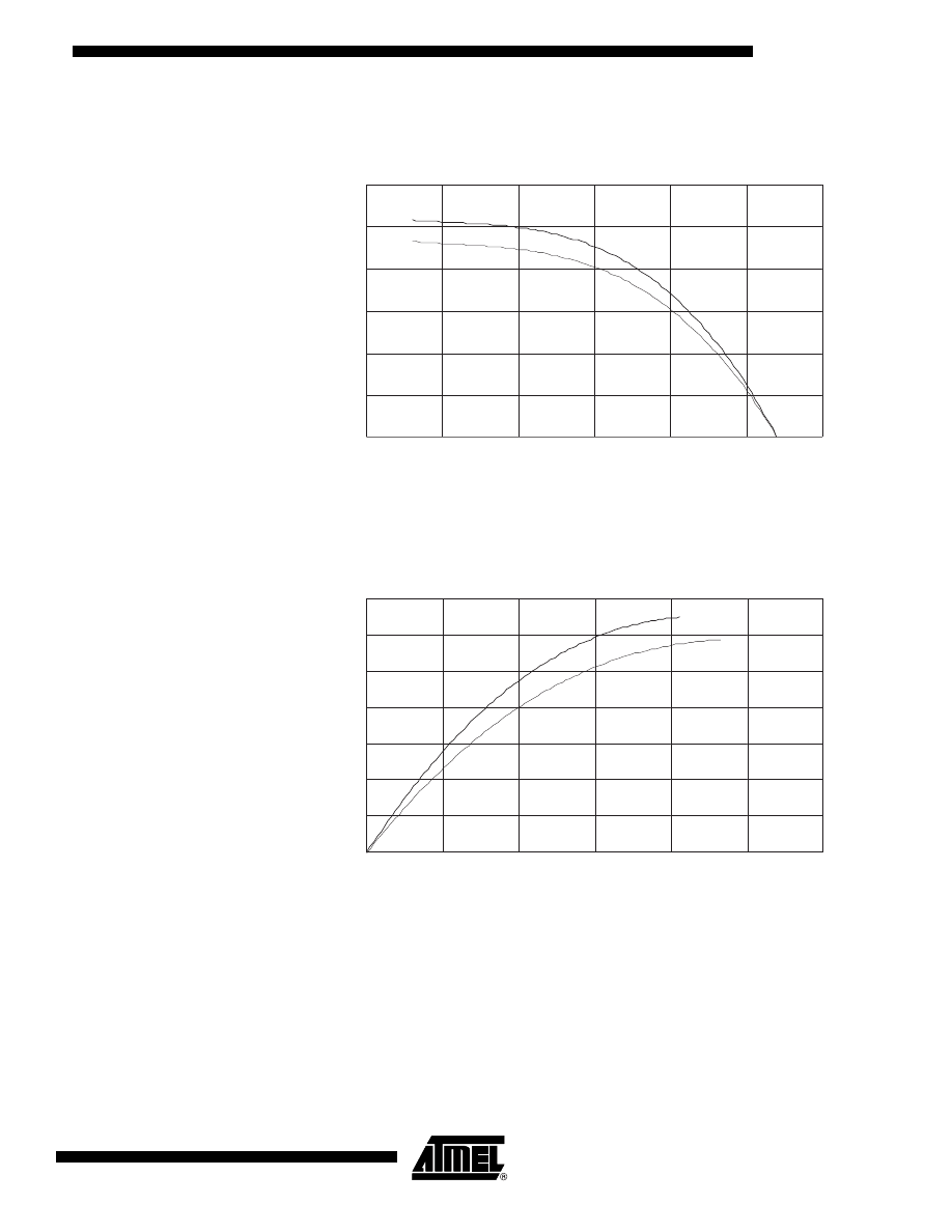
71
ATtiny15L
1187F–AVR–06/05
Figure 45. Pull-up Resistor Current vs. Input Voltage
Figure 46. I/O Pin Sink Current vs. Output Voltage
0
5
10
15
20
25
30
0
0.5
1
1.5
2
2.5
3
PULL-UP RESISTOR CURRENT vs. INPUT VOLTAGE
I (
µ
A)
OP
V (V)
OP
V = 2.7V
cc
T = 85
˚
C
A
T = 25
˚
C
A
0
10
20
30
40
50
60
70
0
0.5
1
1.5
2
2.5
3
V = 5V
cc
I
(mA)
OL
V (V)
OL
T = 85
˚
C
A
T = 25
˚
C
A
I/O PIN SINK CURRENT vs. OUTPUT VOLTAGE

72
ATtiny15L
1187F–AVR–06/05
Figure 47. I/O Pin Source Current vs. Output Voltage
Figure 48. I/O Pin Sink Current vs. Output Voltage
0
2
4
6
8
10
12
14
16
18
20
0
0.5
1
1.5
2
2.5
3
3.5
4
4.5
5
I/O PIN SOURCE CURRENT vs. OUTPUT VOLTAGE
V = 5V
cc
I
(mA)
OH
V (V)
OH
T = 85
˚
C
A
T = 25
˚
C
A
0
5
10
15
20
25
0
0.5
1
1.5
2
I
(mA)
OL
V (V)
OL
T = 85
˚
C
A
T = 25
˚
C
A
I/O PIN SINK CURRENT vs. OUTPUT VOLTAGE
V = 2.7V
cc

73
ATtiny15L
1187F–AVR–06/05
Figure 49. I/O Pin Source Current vs. Output Voltage
Figure 50. I/O Pin Input Threshold Voltage vs. V
CC
0
1
2
3
4
5
6
0
0.5
1
1.5
2
2.5
3
I/O PIN SOURCE CURRENT vs. OUTPUT VOLTAGE
I
(mA)
OH
V (V)
OH
T = 85
˚
C
A
T = 25
˚
C
A
V = 2.7V
cc
0
0.5
1
1.5
2
2.5
2.7
4.0
5.0
Threshold Voltage (V)
V
cc
I/O PIN INPUT THRESHOLD VOLTAGE vs. V
cc
T = 25
˚
C
A

74
ATtiny15L
1187F–AVR–06/05
Figure 51. I/O Pin Input Hysteresis vs. V
CC
0
0.02
0.04
0.06
0.08
0.1
0.12
0.14
0.16
0.18
2.7
4.0
5.0
Input hysteresis (V)
V
cc
I/O PIN INPUT HYSTERESIS vs. V
cc
T = 25
˚
C
A
75
ATtiny15L
1187F–AVR–06/05
ATtiny15L Register Summary
Address
Name
Bit 7
Bit 6
Bit 5
Bit 4
Bit 3
Bit 2
Bit 1
Bit 0
Page
$3F
SREG
I
T
H
S
V
N
Z
C
$3E
Reserved
$3C
Reserved
$3B
GIMSK
-
INT0
PCIE
-
-
-
-
-
$3A
GIFR
-
INTF0
PCIF
-
-
-
-
-
$39
TIMSK
-
OCIE1A
-
-
-
TOIE1
TOIE0
-
$38
TIFR
-
OCF1A
-
-
-
TOV1
TOV0
-
$37
Reserved
$36
Reserved
$35
MCUCR
-
PUD
SE
SM1
SM0
-
ISC01
ISC00
$34
MCUSR
-
-
-
-
WDRF
BORF
EXTRF
PORF
$33
TCCR0
-
-
-
-
-
CS02
CS01
CS00
$32
TCNT0
Timer/Counter0 (8-Bit)
$31
OSCCAL
Oscillator Calibration Register
$30
TCCR1
CTC1
PWM1
COM1A1
COM1A0
CS13
CS12
CS11
CS10
$2F
TCNT1
Timer/Counter1 (8-Bit)
$2E
OCR1A
Timer/Counter1 Output Compare Register A (8-Bit)
$2D
OCR1B
Timer/Counter1 Output Compare Register B (8-Bit)
$2C
SFIOR
-
-
-
-
-
FOC1A
PSR1
PSR0
$2B
Reserved
$2A
Reserved
$29
Reserved
$28
Reserved
$27
Reserved
$26
Reserved
$25
Reserved
$24
Reserved
$23
Reserved
$22
Reserved
$21
WDTCR
-
-
-
WDTOE
WDE
WDP2
WDP1
WDP0
$20
Reserved
$1F
Reserved
$1E
EEAR
-
-
EEAR5
EEAR4
EEAR3
EEAR2
EEAR1
EEAR0
$1D
EEDR
EEPROM Data Register (8-Bit)
$1C
EECR
-
-
-
-
EERIE
EEMWE
EEWE
EERE
$1B
Reserved
$1A
Reserved
$19
Reserved
$18
PORTB
-
-
-
PORTB4
PORTB3
PORTB2
PORTB1
PORTB0
$17
DDRB
-
-
DDB5
DDB4
DDB3
DDB2
DDB1
DDB0
$16
PINB
-
-
PINB5
PINB4
PINB3
PINB2
PINB1
PINB0
$15
Reserved
$14
Reserved
$13
Reserved
$12
Reserved
$11
Reserved
$10
Reserved
$0F
Reserved
$0E
Reserved
$0D
Reserved
$0C
Reserved
$0B
Reserved
$0A
Reserved
$09
Reserved
$08
ACSR
ACD
ACBG
ACO
ACI
ACIE
-
ACIS1
ACIS0
$07
ADMUX
REFS1
REFS0
ADLAR
-
-
MUX2
MUX1
MUX0
$06
ADCSR
ADEN
ADSC
ADFR
ADIF
ADIE
ADPS2
ADPS1
ADPS0
$05
ADCH
ADC Data Register High Byte
$04
ADCL
ADC Data Register Low Byte
…
Reserved
$00
Reserved

76
ATtiny15L
1187F–AVR–06/05
ATtiny15L Instruction Set Summary
Mnemonic
Operands
Description
Operation
Flags
# Clocks
ARITHMETIC AND LOGIC INSTRUCTIONS
ADD
Rd, Rr
Add Two Registers
Rd
← Rd + Rr
Z,C,N,V,H
1
ADC
Rd, Rr
Add with Carry Two Registers
Rd
← Rd + Rr + C
Z,C,N,V,H
1
SUB
Rd, Rr
Subtract Two Registers
Rd
← Rd - Rr
Z,C,N,V,H
1
SUBI
Rd, K
Subtract Constant from Register
Rd
← Rd - K
Z,C,N,V,H
1
SBC
Rd, Rr
Subtract with Carry Two Registers
Rd
← Rd - Rr - C
Z,C,N,V,H
1
SBCI
Rd, K
Subtract with Carry Constant from Reg.
Rd
← Rd - K - C
Z,C,N,V,H
1
AND
Rd, Rr
Logical AND Registers
Rd
← Rd • Rr
Z,N,V
1
ANDI
Rd, K
Logical AND Register and Constant
Rd
← Rd • K
Z,N,V
1
OR
Rd, Rr
Logical OR Registers
Rd
← Rd v Rr
Z,N,V
1
ORI
Rd, K
Logical OR Register and Constant
Rd
← Rd v K
Z,N,V
1
EOR
Rd, Rr
Exclusive OR Registers
Rd
← Rd⊕Rr
Z,N,V
1
COM
Rd
One’s Complement
Rd
← $FF - Rd
Z,C,N,V
1
NEG
Rd
Two’s Complement
Rd
← $00 - Rd
Z,C,N,V,H
1
SBR
Rd, K
Set Bit(s) in Register
Rd
← Rd v K
Z,N,V
1
CBR
Rd, K
Clear Bit(s) in Register
Rd
← Rd • (FFh - K)
Z,N,V
1
INC
Rd
Increment
Rd
← Rd + 1
Z,N,V
1
DEC
Rd
Decrement
Rd
← Rd - 1
Z,N,V
1
TST
Rd
Test for Zero or Minus
Rd
← Rd • Rd Z,N,V
1
CLR
Rd
Clear Register
Rd
← Rd⊕Rd
Z,N,V
1
SER
Rd
Set Register
Rd
← $FF
None
1
BRANCH INSTRUCTIONS
RJMP
k
Relative Jump
PC
← PC + k + 1
None
2
RCALL
k
Relative Subroutine Call
PC
← PC + k + 1
None
3
RET
Subroutine Return
PC
← STACK
None
4
RETI
Interrupt Return
PC
← STACK
I
4
CPSE
Rd, Rr
Compare, Skip if Equal
if (Rd = Rr) PC
← PC + 2 or 3
None
1/2
CP
Rd, Rr
Compare
Rd - Rr
Z,N,V,C,H
1
CPC
Rd, Rr
Compare with Carry
Rd - Rr - C
Z,N,V,C,H
1
CPI
Rd, K
Compare Register with Immediate
Rd - K
Z,N,V,C,H
1
SBRC
Rr, b
Skip if Bit in Register Cleared
if (Rr(b) = 0) PC
← PC + 2 or 3
None
1/2
SBRS
Rr, b
Skip if Bit in Register is Set
if (Rr(b) = 1) PC
← PC + 2 or 3
None
1/2
SBIC
P, b
Skip if Bit in I/O Register Cleared
if (P(b) = 0) PC
← PC + 2 or 3
None
1/2
SBIS
P, b
Skip if Bit in I/O Register is Set
if (P(b) = 1) PC
← PC + 2 or 3
None
1/2
BRBS
s, k
Branch if Status Flag Set
if (SREG(s) = 1) then PC
← PC + k + 1
None
1/2
BRBC
s, k
Branch if Status Flag Cleared
if (SREG(s) = 0) then PC
← PC + k + 1
None
1/2
BREQ
k
Branch if Equal
if (Z = 1) then PC
← PC + k + 1
None
1/2
BRNE
k
Branch if Not Equal
if (Z = 0) then PC
← PC + k + 1
None
1/2
BRCS
k
Branch if Carry Set
if (C = 1) then PC
← PC + k + 1
None
1/2
BRCC
k
Branch if Carry Cleared
if (C = 0) then PC
← PC + k + 1
None
1/2
BRSH
k
Branch if Same or Higher
if (C = 0) then PC
← PC + k + 1
None
1/2
BRLO
k
Branch if Lower
if (C = 1) then PC
← PC + k + 1
None
1/2
BRMI
k
Branch if Minus
if (N = 1) then PC
← PC + k + 1
None
1/2
BRPL
k
Branch if Plus
if (N = 0) then PC
← PC + k + 1
None
1/2
BRGE
k
Branch if Greater or Equal, Signed
if (N
⊕ V= 0) then PC ← PC + k + 1
None
1/2
BRLT
k
Branch if Less Than Zero, Signed
if (N
⊕ V= 1) then PC ← PC + k + 1
None
1/2
BRHS
k
Branch if Half-carry Flag Set
if (H = 1) then PC
← PC + k + 1
None
1/2
BRHC
k
Branch if Half-carry Flag Cleared
if (H = 0) then PC
← PC + k + 1
None
1/2
BRTS
k
Branch if T-flag Set
if (T = 1) then PC
← PC + k + 1
None
1/2
BRTC
k
Branch if T-flag Cleared
if (T = 0) then PC
← PC + k + 1
None
1/2
BRVS
k
Branch if Overflow Flag is Set
if (V = 1) then PC
← PC + k + 1
None
1/2
BRVC
k
Branch if Overflow Flag is Cleared
if (V = 0) then PC
← PC + k + 1
None
1/2
BRIE
k
Branch if Interrupt Enabled
if (I = 1) then PC
← PC + k + 1
None
1/2
BRID
k
Branch if Interrupt Disabled
if (I = 0) then PC
← PC + k + 1
None
1/2
DATA TRANSFER INSTRUCTIONS
LD
Rd, Z
Load Register Indirect
Rd
← (Z)
None
2
ST
Z, Rr
Store Register Indirect
(Z)
← Rr
None
2
MOV
Rd, Rr
Move between Registers
Rd
← Rr
None
1
LDI
Rd, K
Load Immediate
Rd
← K
None
1
IN
Rd, P
In Port
Rd
← P
None
1
OUT
P, Rr
Out Port
P
← Rr
None
1
LPM
Load Program Memory
R0
← (Z)
None
3
BIT AND BIT-TEST INSTRUCTIONS
SBI
P, b
Set Bit in I/O Register
I/O(P,b)
← 1
None
2

77
ATtiny15L
1187F–AVR–06/05
CBI
P, b
Clear Bit in I/O Register
I/O(P,b)
← 0
None
2
LSL
Rd
Logical Shift Left
Rd(n+1)
← Rd(n), Rd(0) ← 0
Z,C,N,V
1
LSR
Rd
Logical Shift Right
Rd(n)
← Rd(n+1), Rd(7) ← 0
Z,C,N,V
1
ROL
Rd
Rotate Left through Carry
Rd(0)
← C, Rd(n+1) ← Rd(n), C ← Rd(7)
Z,C,N,V
1
ROR
Rd
Rotate Right through Carry
Rd(7)
← C, Rd(n) ← Rd(n+1), C ← Rd(0)
Z,C,N,V
1
ASR
Rd
Arithmetic Shift Right
Rd(n)
← Rd(n+1), n = 0..6
Z,C,N,V
1
SWAP
Rd
Swap Nibbles
Rd(3..0)
← Rd(7..4), Rd(7..4) ← Rd(3..0)
None
1
BSET
s
Flag Set
SREG(s)
← 1
SREG(s)
1
BCLR
s
Flag Clear
SREG(s)
← 0
SREG(s)
1
BST
Rr, b
Bit Store from Register to T
T
← Rr(b)
T
1
BLD
Rd, b
Bit Load from T to Register
Rd(b)
← T
None
1
SEC
Set Carry
C
← 1
C
1
CLC
Clear Carry
C
← 0
C
1
SEN
Set Negative Flag
N
← 1
N
1
CLN
Clear Negative Flag
N
← 0
N
1
SEZ
Set Zero Flag
Z
← 1
Z
1
CLZ
Clear Zero Flag
Z
← 0
Z
1
SEI
Global Interrupt Enable
I
← 1
I
1
CLI
Global Interrupt Disable
I
← 0
I
1
SES
Set Signed Test Flag
S
← 1
S
1
CLS
Clear Signed Test Flag
S
← 0
S
1
SEV
Set Two’s Complement Overflow
V
← 1
V
1
CLV
Clear Two’s Complement Overflow
V
← 0
V
1
SET
Set T in SREG
T
← 1
T
1
CLT
Clear T in SREG
T
← 0
T
1
SEH
Set Half-carry Flag in SREG
H
← 1
H
1
CLH
Clear Half-carry Flag in SREG
H
← 0
H
1
NOP
No Operation
None
1
SLEEP
Sleep
(see specific descr. for Sleep function)
None
1
WDR
Watchdog Reset
(see specific descr. for WDR/timer)
None
1
ATtiny15L Instruction Set Summary (Continued)
Mnemonic
Operands
Description
Operation
Flags
# Clocks

78
ATtiny15L
1187F–AVR–06/05
Ordering Information
Power Supply
Speed (MHz)
Ordering Code
Package
Operation Range
2.7 - 5.5V
1.6
ATtiny15L-1PC
ATtiny15L-1SC
8P3
8S2
Commercial
(0
°C to 70°C)
ATtiny15L-1PI
ATtiny15L-1SI
8P3
8S2
Industrial
(-40
°C to 85°C)
Package Type
8P3
8-lead, 0.300" Wide, Plastic Dual Inline Package (PDIP)
8S2
8-lead, 0.200" Wide, Plastic Gull Wing Small Outline (EIAJ SOIC)
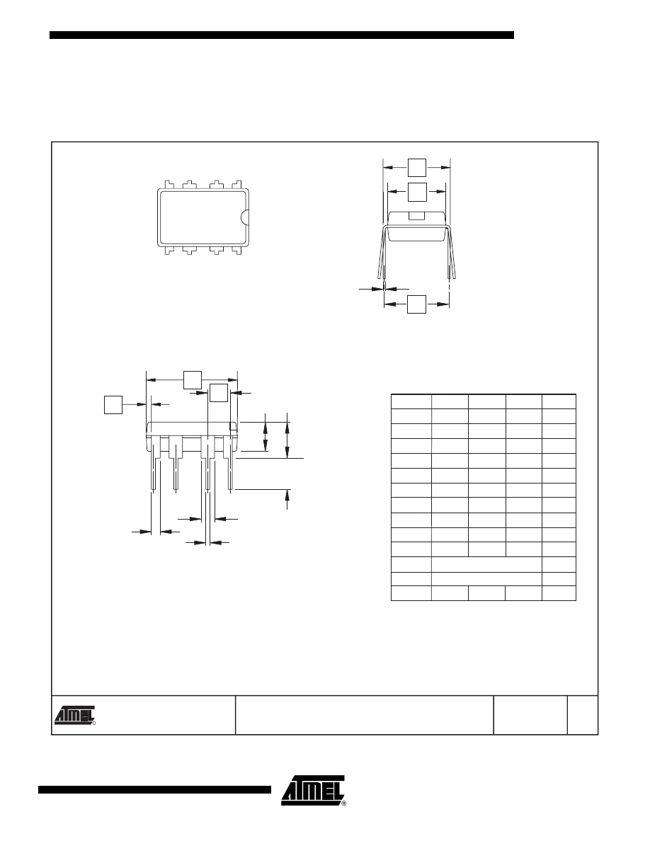
79
ATtiny15L
1187F–AVR–06/05
Packaging Information
8P3
2325 Orchard Parkway
San Jose, CA 95131
TITLE
DRAWING NO.
R
REV.
8P3, 8-lead, 0.300" Wide Body, Plastic Dual
In-line Package (PDIP)
01/09/02
8P3
B
D
D1
E
E1
e
L
b2
b
A2 A
1
N
eA
c
b3
4 PLCS
Top View
Side View
End View
COMMON DIMENSIONS
(Unit of Measure = inches)
SYMBOL
MIN
NOM
MAX
NOTE
Notes:
1. This drawing is for general information only; refer to JEDEC Drawing MS-001, Variation BA for additional information.
2. Dimensions A and L are measured with the package seated in JEDEC seating plane Gauge GS-3.
3. D, D1 and E1 dimensions do not include mold Flash or protrusions. Mold Flash or protrusions shall not exceed 0.010 inch.
4. E and eA measured with the leads constrained to be perpendicular to datum.
5. Pointed or rounded lead tips are preferred to ease insertion.
6. b2 and b3 maximum dimensions do not include Dambar protrusions. Dambar protrusions shall not exceed 0.010 (0.25 mm).
A
0.210
2
A2
0.115
0.130
0.195
b
0.014
0.018
0.022
5
b2
0.045
0.060
0.070
6
b3
0.030
0.039
0.045
6
c
0.008
0.010
0.014
D
0.355
0.365
0.400
3
D1
0.005
3
E
0.300
0.310
0.325
4
E1
0.240
0.250
0.280
3
e
0.100 BSC
eA
0.300 BSC
4
L
0.115
0.130
0.150
2
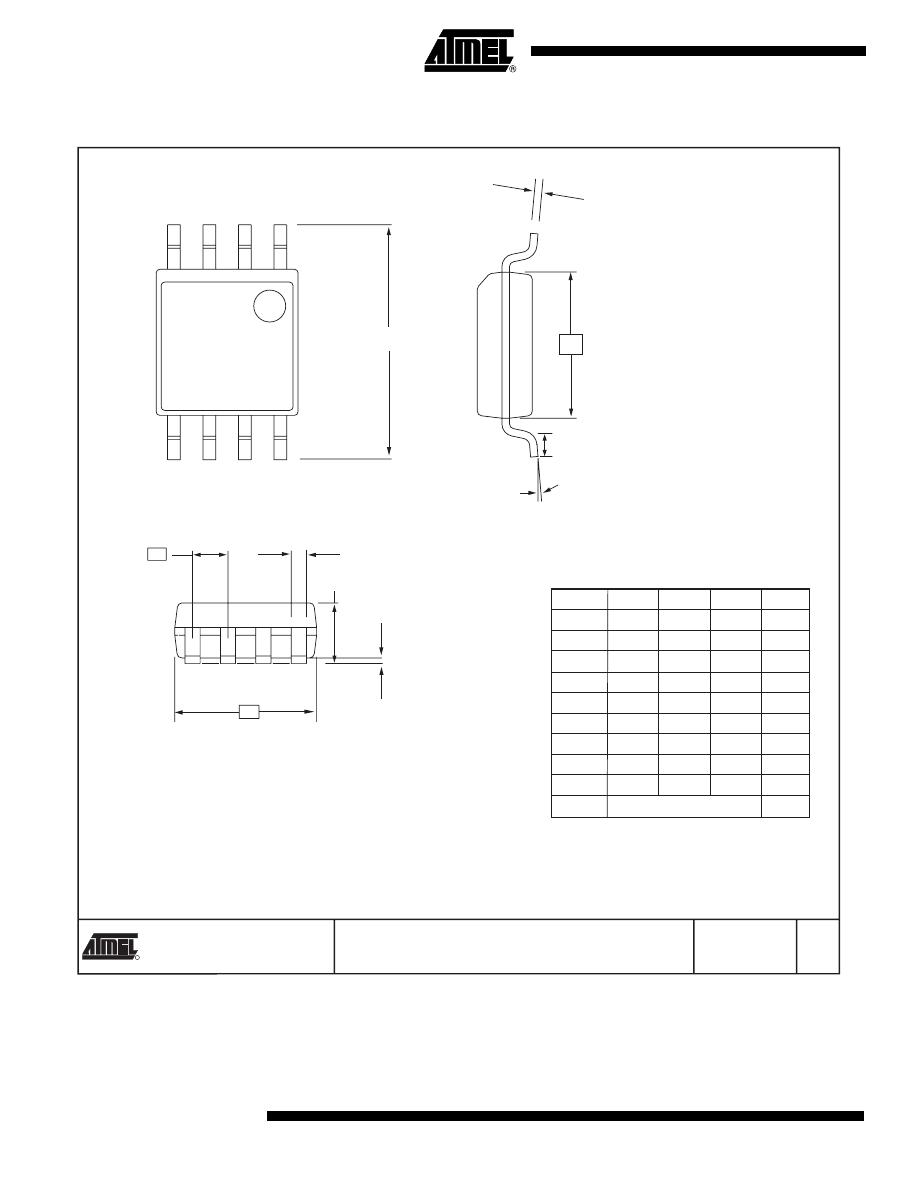
80
ATtiny15L
1187F–AVR–06/05
8S2
2325 Orchard Parkway
San Jose, CA 95131
TITLE
DRAWING NO.
R
REV.
8S2, 8-lead, 0.209" Body, Plastic Small
Outline Package (EIAJ)
10/7/03
8S2
C
COMMON DIMENSIONS
(Unit of Measure = mm)
SYMBOL
MIN
NOM
MAX
NOTE
Notes: 1. This drawing is for general information only; refer to EIAJ Drawing EDR-7320 for additional information.
2. Mismatch of the upper and lower dies and resin burrs are not included.
3. It is recommended that upper and lower cavities be equal. If they are different, the larger dimension shall be regarded.
4. Determines the true geometric position.
5. Values b and C apply to pb/Sn solder plated terminal. The standard thickness of the solder layer shall be 0.010 +0.010/
−0.005 mm.
A 1.70
2.16
A1 0.05
0.25
b
0.35
0.48 5
C
0.15
0.35 5
D 5.13
5.35
E1 5.18
5.40 2,
3
E 7.70
8.26
L 0.51
0.85
∅
0˚
8˚
e
1.27 BSC
4
End View
Side View
e
b
A
A1
D
E
N
1
C
E1
∅
L
Top View

81
ATtiny15L
1187F–AVR–06/05
Datasheet revision
history
Rev F - 06/05
1. Updated V
BOT
.
2. Added “Unconnected Pins” on page 51.
3. Updated “Packaging Information” on page 79.

82
ATtiny15L
1187F–AVR–06/05

i
ATtiny15L
1187F–AVR–06/05
Table of Contents
ATtiny15L Architectural Overview ...................................................... 5
The Program and Data Addressing Modes .......................................................... 7
Internal PLL for Fast Peripheral Clock Generation ............................................. 24
The Special Function IO Register – SFIOR........................................................ 26
The Watchdog Timer .......................................................................... 34
EEPROM Read/Write Access ............................................................. 36
The Analog Comparator ..................................................................... 39

ii
ATtiny15L
1187F–AVR–06/05
Memory Programming........................................................................ 54
High-voltage Serial Programming Algorithm....................................................... 56
High-voltage Serial Programming Characteristics .............................................. 59
Low-voltage Serial Programming Characteristics............................................... 63
Electrical Characteristics................................................................... 64
Typical Characteristics ...................................................................... 66
ATtiny15L Register Summary............................................................ 75
ATtiny15L Instruction Set Summary ................................................. 76
Ordering Information .......................................................................... 78
Packaging Information ....................................................................... 79
Datasheet revision history ................................................................. 81

Printed on recycled paper.
1187F–AVR–06/05
Disclaimer: The information in this document is provided in connection with Atmel products. No license, express or implied, by estoppel or otherwise, to any
intellectual property right is granted by this document or in connection with the sale of Atmel products. EXCEPT AS SET FORTH IN ATMEL’S TERMS AND CONDI-
TIONS OF SALE LOCATED ON ATMEL’S WEB SITE, ATMEL ASSUMES NO LIABILITY WHATSOEVER AND DISCLAIMS ANY EXPRESS, IMPLIED OR STATUTORY
WARRANTY RELATING TO ITS PRODUCTS INCLUDING, BUT NOT LIMITED TO, THE IMPLIED WARRANTY OF MERCHANTABILITY, FITNESS FOR A PARTICULAR
PURPOSE, OR NON-INFRINGEMENT. IN NO EVENT SHALL ATMEL BE LIABLE FOR ANY DIRECT, INDIRECT, CONSEQUENTIAL, PUNITIVE, SPECIAL OR INCIDEN-
TAL DAMAGES (INCLUDING, WITHOUT LIMITATION, DAMAGES FOR LOSS OF PROFITS, BUSINESS INTERRUPTION, OR LOSS OF INFORMATION) ARISING OUT
OF THE USE OR INABILITY TO USE THIS DOCUMENT, EVEN IF ATMEL HAS BEEN ADVISED OF THE POSSIBILITY OF SUCH DAMAGES. Atmel makes no
representations or warranties with respect to the accuracy or completeness of the contents of this document and reserves the right to make changes to specifications
and product descriptions at any time without notice. Atmel does not make any commitment to update the information contained herein. Atmel’s products are not
intended, authorized, or warranted for use as components in applications intended to support or sustain life.
Atmel Corporation
Atmel Operations
2325 Orchard Parkway
San Jose, CA 95131, USA
Tel: 1(408) 441-0311
Fax: 1(408) 487-2600
Regional Headquarters
Europe
Atmel Sarl
Route des Arsenaux 41
Case Postale 80
CH-1705 Fribourg
Switzerland
Tel: (41) 26-426-5555
Fax: (41) 26-426-5500
Asia
Room 1219
Chinachem Golden Plaza
77 Mody Road Tsimshatsui
East Kowloon
Hong Kong
Tel: (852) 2721-9778
Fax: (852) 2722-1369
Japan
9F, Tonetsu Shinkawa Bldg.
1-24-8 Shinkawa
Chuo-ku, Tokyo 104-0033
Japan
Tel: (81) 3-3523-3551
Fax: (81) 3-3523-7581
Memory
2325 Orchard Parkway
San Jose, CA 95131, USA
Tel: 1(408) 441-0311
Fax: 1(408) 436-4314
Microcontrollers
2325 Orchard Parkway
San Jose, CA 95131, USA
Tel: 1(408) 441-0311
Fax: 1(408) 436-4314
La Chantrerie
BP 70602
44306 Nantes Cedex 3, France
Tel: (33) 2-40-18-18-18
Fax: (33) 2-40-18-19-60
ASIC/ASSP/Smart Cards
Zone Industrielle
13106 Rousset Cedex, France
Tel: (33) 4-42-53-60-00
Fax: (33) 4-42-53-60-01
1150 East Cheyenne Mtn. Blvd.
Colorado Springs, CO 80906, USA
Tel: 1(719) 576-3300
Fax: 1(719) 540-1759
Scottish Enterprise Technology Park
Maxwell Building
East Kilbride G75 0QR, Scotland
Tel: (44) 1355-803-000
Fax: (44) 1355-242-743
RF/Automotive
Theresienstrasse 2
Postfach 3535
74025 Heilbronn, Germany
Tel: (49) 71-31-67-0
Fax: (49) 71-31-67-2340
1150 East Cheyenne Mtn. Blvd.
Colorado Springs, CO 80906, USA
Tel: 1(719) 576-3300
Fax: 1(719) 540-1759
Biometrics/Imaging/Hi-Rel MPU/
High Speed Converters/RF Datacom
Avenue de Rochepleine
BP 123
38521 Saint-Egreve Cedex, France
Tel: (33) 4-76-58-30-00
Fax: (33) 4-76-58-34-80
Literature Requests
www.atmel.com/literature
© Atmel Corporation 2005. All rights reserved. Atmel
®
, logo and combinations thereof, Everywhere You Are
®
, AVR
®
, AVR Studio
®
, and others
are the registered trademarks of Atmel Corporation or its subsidiaries. Other terms and product names may be trademarks of others.
Document Outline
- Features
- Pin Configuration
- Description
- ATtiny15L Architectural Overview
- The General Purpose Register File
- The ALU - Arithmetic Logic Unit
- The Flash Program Memory
- The Program and Data Addressing Modes
- Subroutine and Interrupt Hardware Stack
- The EEPROM Data Memory
- I/O Memory
- Reset and Interrupt Handling
- Internal Voltage Reference
- Interrupt Handling
- Sleep Modes
- Tuneable Internal RC Oscillator
- Internal PLL for Fast Peripheral Clock Generation
- Timer/Counters
- The Watchdog Timer
- EEPROM Read/Write Access
- The Analog Comparator
- The Analog-to-Digital Converter, Analog Multiplexer, and Gain Stages
- I/O Port B
- Memory Programming
- Electrical Characteristics
- Typical Characteristics
- ATtiny15L Register Summary
- ATtiny15L Instruction Set Summary
- Ordering Information
- Packaging Information
- Datasheet revision history
- Table of Contents
Wyszukiwarka
Podobne podstrony:
HD44780 ATTINY13 BOARD TOP MIRROR
Attiny 28L opis
fetch datenblatt attiny26
Attiny 2313 opis
A09 0797 QT600 ATTINY88 QT8 sch
Installing Attiny13 core files
ATtiny13
Instrukcja instalacji Arduino na AtTiny13
AVR091 Replacing AT90S2313 with ATtiny2313
ATtiny25 45 85
ATTINY2313
HD44780 ATTINY13 SCHEMATIC
Attiny 13 opis
ATTINY22 id 71984 Nieznany (2)
ATtiny28L ATtiny28V
HD44780 ATTINY13 BOARD TOP
HD44780 ATTINY13 BOARD TOP MIRROR
Attiny 28L opis
więcej podobnych podstron