
Features
•
High Performance, Low Power AVR
®
8-Bit Microcontroller
•
Advanced RISC Architecture
– 120 Powerful Instructions – Most Single Clock Cycle Execution
– 32 x 8 General Purpose Working Registers
– Fully Static Operation
– Up to 20 MIPS Througput at 20 MHz
•
High Endurance Non-volatile Memory segments
– 1K Bytes of In-System Self-programmable Flash program memory
– 64 Bytes EEPROM
– 64 Bytes Internal SRAM
– Write/Erase cyles: 10,000 Flash/100,000 EEPROM
– Data retention: 20 years at 85°C/100 years at 25°C (see
– Programming Lock for Self-Programming Flash & EEPROM Data Security
•
Peripheral Features
– One 8-bit Timer/Counter with Prescaler and Two PWM Channels
– 4-channel, 10-bit ADC with Internal Voltage Reference
– Programmable Watchdog Timer with Separate On-chip Oscillator
– On-chip Analog Comparator
•
Special Microcontroller Features
– debugWIRE On-chip Debug System
– In-System Programmable via SPI Port
– External and Internal Interrupt Sources
– Low Power Idle, ADC Noise Reduction, and Power-down Modes
– Enhanced Power-on Reset Circuit
– Programmable Brown-out Detection Circuit
– Internal Calibrated Oscillator
•
I/O and Packages
– 8-pin PDIP/SOIC: Six Programmable I/O Lines
– 20-pad MLF: Six Programmable I/O Lines
•
Operating Voltage:
– 1.8 - 5.5V for ATtiny13V
– 2.7 - 5.5V for ATtiny13
•
Speed Grade
– ATtiny13V: 0 - 4 MHz @ 1.8 - 5.5V, 0 - 10 MHz @ 2.7 - 5.5V
– ATtiny13: 0 - 10 MHz @ 2.7 - 5.5V, 0 - 20 MHz @ 4.5 - 5.5V
•
Industrial Temperature Range
•
Low Power Consumption
– Active Mode:
• 1 MHz, 1.8V: 240 µA
– Power-down Mode:
• < 0.1 µA at 1.8V
8-bit
Microcontroller
with 1K Bytes
In-System
Programmable
Flash
ATtiny13
ATtiny13V
Rev. 2535J–AVR–08/10
2
2535J–AVR–08/10
ATtiny13
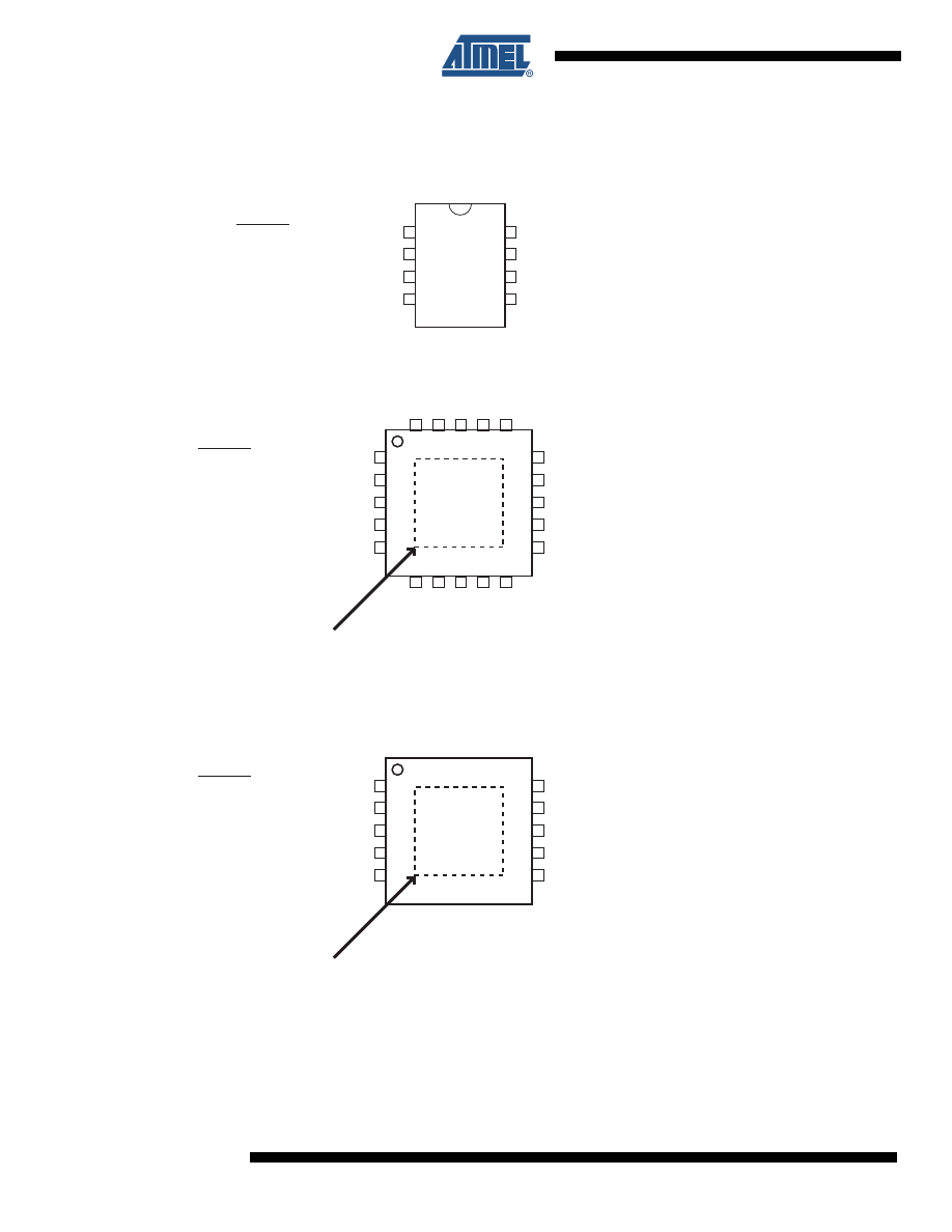
1. Pin Configurations
Figure 1-1.
Pinout ATtiny13/ATtiny13V
1
2
3
4
8
7
6
5
(PCINT5/RESET/ADC0/dW) PB5
(PCINT3/CLKI/ADC3) PB3
(PCINT4/ADC2) PB4
GND
VCC
PB2 (SCK/ADC1/T0/PCINT2)
PB1 (MISO/AIN1/OC0B/INT0/PCINT1)
PB0 (MOSI/AIN0/OC0A/PCINT0)
8-PDIP/SOIC
1
2
3
4
5
20-QFN/MLF
15
14
13
12
11
20
19
18
17
16
6
7
8
9
10
(PCINT5/RESET/ADC0/dW) PB5
(PCINT3/CLKI/ADC3) PB3
DNC
DNC
(PCINT4/ADC2) PB4
DNC
DNC
GND
DNC
DNC
VCC
PB2 (SCK/ADC1/T0/PCINT2)
DNC
PB1 (MISO/AIN1/OC0B/INT0/PCINT1)
PB0 (MOSI/AIN0/OC0A/PCINT0)
DNC
DNC
DNC
DNC
DNC
NOTE: Bottom pad should be soldered to ground.
DNC: Do Not Connect
1
2
3
4
5
10-QFN/MLF
10
9
8
7
6
(PCINT5/RESET/ADC0/dW) PB5
(PCINT3/CLKI/ADC3) PB3
DNC
(PCINT4/ADC2) PB4
GND
VCC
PB2 (SCK/ADC1/T0/PCINT2)
DNC
PB1 (MISO/AIN1/OC0B/INT0/PCINT1)
PB0 (MOSI/AIN0/OC0A/PCINT0)
NOTE: Bottom pad should be soldered to ground.
DNC: Do Not Connect

3
2535J–AVR–08/10
ATtiny13
1.1
Pin Descriptions
1.1.1
VCC
Digital supply voltage.
1.1.2
GND
Ground.
1.1.3
Port B (PB5:PB0)
Port B is a 6-bit bi-directional I/O port with internal pull-up resistors (selected for each bit). The
Port B output buffers have symmetrical drive characteristics with both high sink and source
capability. As inputs, Port B pins that are externally pulled low will source current if the pull-up
resistors are activated. The Port B pins are tri-stated when a reset condition becomes active,
even if the clock is not running.
Port B also serves the functions of various special features of the ATtiny13 as listed on
1.1.4
RESET
Reset input. A low level on this pin for longer than the minimum pulse length will generate a
reset, even if the clock is not running. The minimum pulse length is given in
. Shorter pulses are not guaranteed to generate a reset.
The reset pin can also be used as a (weak) I/O pin.
4
2535J–AVR–08/10
ATtiny13
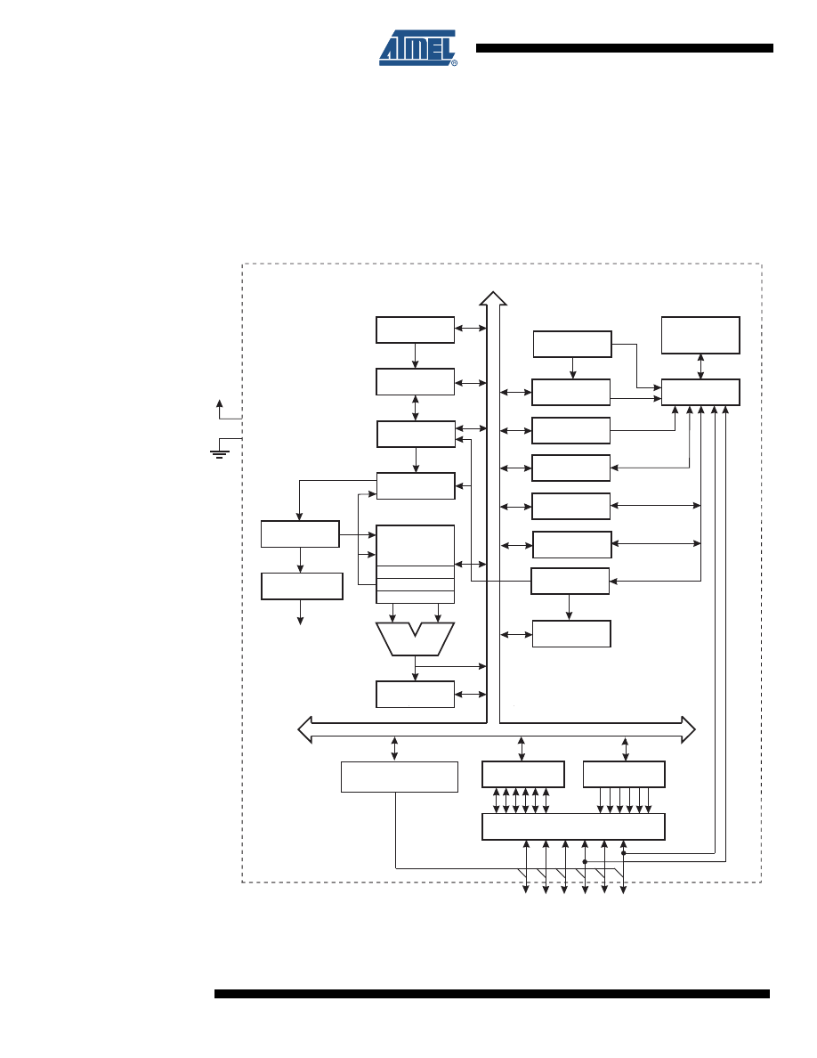
2. Overview
The ATtiny13 is a low-power CMOS 8-bit microcontroller based on the AVR enhanced RISC
architecture. By executing powerful instructions in a single clock cycle, the ATtiny13 achieves
throughputs approaching 1 MIPS per MHz allowing the system designer to optimize power con-
sumption versus processing speed.
2.1
Block Diagram
Figure 2-1.
Block Diagram
PROGRAM
COUNTER
INTERNAL
OSCILLATOR
WATCHDOG
TIMER
STACK
POINTER
PROGRAM
FLASH
SRAM
MCU CONTROL
REGISTER
GENERAL
PURPOSE
REGISTERS
INSTRUCTION
REGISTER
TIMER/
COUNTER0
INSTRUCTION
DECODER
DATA DIR.
REG.PORT B
DATA REGISTER
PORT B
PROGRAMMING
LOGIC
TIMING AND
CONTROL
MCU STATUS
REGISTER
STATUS
REGISTER
ALU
PORT B DRIVERS
PB0-PB5
VCC
GND
CONTROL
LINES
8-BIT DATABUS
Z
ADC /
ANALOG COMPARATOR
INTERRUPT
UNIT
CALIBRATED
Y
X
RESET
CLKI
WATCHDOG
OSCILLATOR
DATA
EEPROM

5
2535J–AVR–08/10
ATtiny13
The AVR core combines a rich instruction set with 32 general purpose working registers. All 32
registers are directly connected to the Arithmetic Logic Unit (ALU), allowing two independent
registers to be accessed in one single instruction executed in one clock cycle. The resulting
architecture is more code efficient while achieving throughputs up to ten times faster than con-
ventional CISC microcontrollers.
The ATtiny13 provides the following features: 1K byte of In-System Programmable Flash, 64
bytes EEPROM, 64 bytes SRAM, 6 general purpose I/O lines, 32 general purpose working reg-
isters, one 8-bit Timer/Counter with compare modes, Internal and External Interrupts, a 4-
channel, 10-bit ADC, a programmable Watchdog Timer with internal Oscillator, and three soft-
ware selectable power saving modes. The Idle mode stops the CPU while allowing the SRAM,
Timer/Counter, ADC, Analog Comparator, and Interrupt system to continue functioning. The
Power-down mode saves the register contents, disabling all chip functions until the next Inter-
rupt or Hardware Reset. The ADC Noise Reduction mode stops the CPU and all I/O modules
except ADC, to minimize switching noise during ADC conversions.
The device is manufactured using Atmel’s high density non-volatile memory technology. The
On-chip ISP Flash allows the Program memory to be re-programmed In-System through an SPI
serial interface, by a conventional non-volatile memory programmer or by an On-chip boot code
running on the AVR core.
The ATtiny13 AVR is supported with a full suite of program and system development tools
including: C Compilers, Macro Assemblers, Program Debugger/Simulators, and Evaluation kits.

6
2535J–AVR–08/10
ATtiny13
3. General Information
3.1
Resources
A comprehensive set of drivers, application notes, data sheets and descriptions on development
tools are available for download at http://www.atmel.com/avr.
3.2
Code Examples
This documentation contains simple code examples that briefly show how to use various parts of
the device. These code examples assume that the part specific header file is included before
compilation. Be aware that not all C compiler vendors include bit definitions in the header files
and interrupt handling in C is compiler dependent. Please confirm with the C compiler documen-
tation for more details.
3.3
Data Retention
Reliability Qualification results show that the projected data retention failure rate is much less
than 1 PPM over 20 years at 85°C or 100 years at 25
°C.
7
2535J–AVR–08/10
ATtiny13
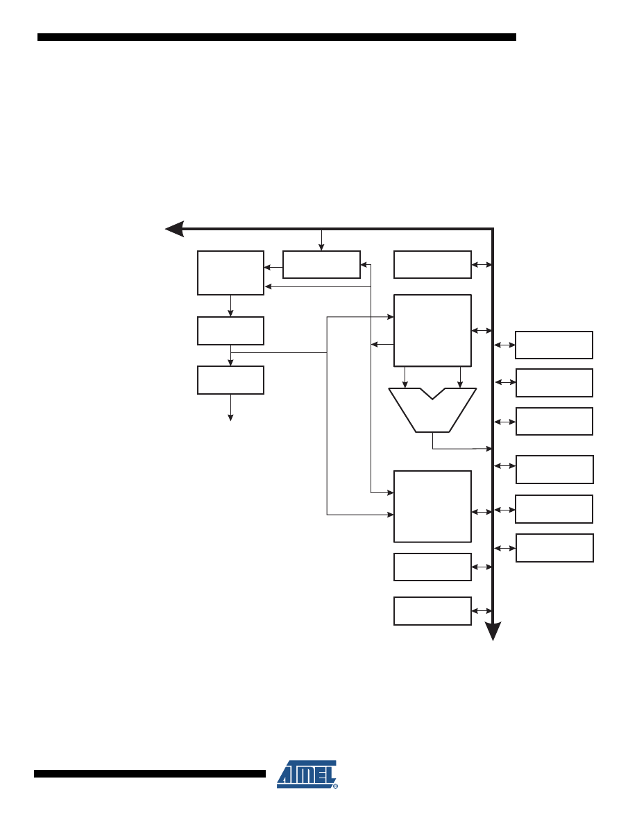
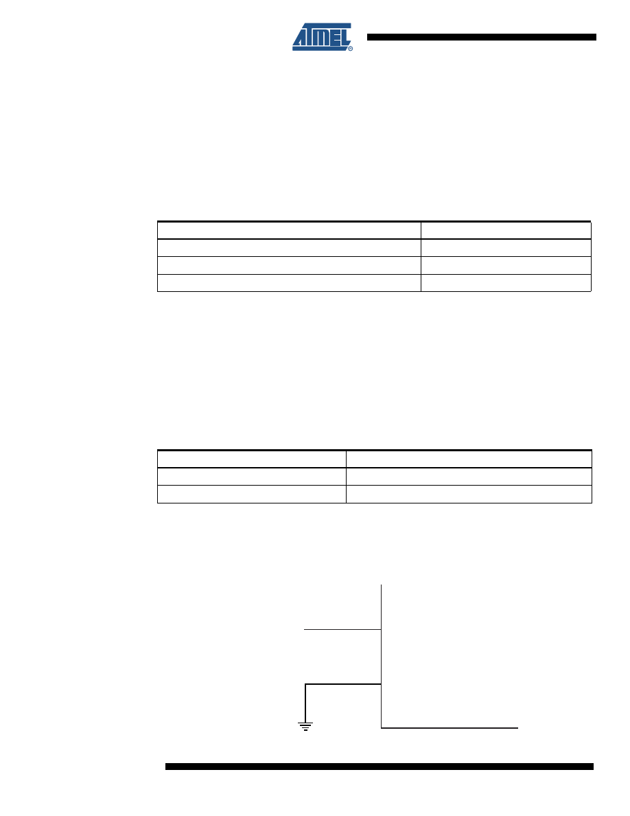
4. CPU Core
This section discusses the AVR core architecture in general. The main function of the CPU core
is to ensure correct program execution. The CPU must therefore be able to access memories,
perform calculations, control peripherals, and handle interrupts.
4.1
Architectural Overview
Figure 4-1.
Block Diagram of the AVR Architecture
In order to maximize performance and parallelism, the AVR uses a Harvard architecture – with
separate memories and buses for program and data. Instructions in the Program memory are
executed with a single level pipelining. While one instruction is being executed, the next instruc-
tion is pre-fetched from the Program memory. This concept enables instructions to be executed
in every clock cycle. The Program memory is In-System Reprogrammable Flash memory.
Flash
Program
Memory
Instruction
Register
Instruction
Decoder
Program
Counter
Control Lines
32 x 8
General
Purpose
Registrers
ALU
Status
and Control
I/O Lines
EEPROM
Data Bus 8-bit
Data
SRAM
Direct Addressing
Indirect Addressing
Interrupt
Unit
Watchdog
Timer
Analog
Comparator
I/O Module 2
I/O Module1
I/O Module n

8
2535J–AVR–08/10
ATtiny13
The fast-access Register File contains 32 x 8-bit general purpose working registers with a single
clock cycle access time. This allows single-cycle Arithmetic Logic Unit (ALU) operation. In a typ-
ical ALU operation, two operands are output from the Register File, the operation is executed,
and the result is stored back in the Register File – in one clock cycle.
Six of the 32 registers can be used as three 16-bit indirect address register pointers for Data
Space addressing – enabling efficient address calculations. One of the these address pointers
can also be used as an address pointer for look up tables in Flash Program memory. These
added function registers are the 16-bit X-, Y-, and Z-register, described later in this section.
The ALU supports arithmetic and logic operations between registers or between a constant and
a register. Single register operations can also be executed in the ALU. After an arithmetic opera-
tion, the Status Register is updated to reflect information about the result of the operation.
Program flow is provided by conditional and unconditional jump and call instructions, able to
directly address the whole address space. Most AVR instructions have a single 16-bit word for-
mat. Every Program memory address contains a 16- or 32-bit instruction.
During interrupts and subroutine calls, the return address Program Counter (PC) is stored on the
Stack. The Stack is effectively allocated in the general data SRAM, and consequently the Stack
size is only limited by the total SRAM size and the usage of the SRAM. All user programs must
initialize the SP in the Reset routine (before subroutines or interrupts are executed). The Stack
Pointer (SP) is read/write accessible in the I/O space. The data SRAM can easily be accessed
through the five different addressing modes supported in the AVR architecture.
The memory spaces in the AVR architecture are all linear and regular memory maps.
A flexible interrupt module has its control registers in the I/O space with an additional Global
Interrupt Enable bit in the Status Register. All interrupts have a separate Interrupt Vector in the
Interrupt Vector table. The interrupts have priority in accordance with their Interrupt Vector posi-
tion. The lower the Interrupt Vector address, the higher the priority.
The I/O memory space contains 64 addresses for CPU peripheral functions as Control Regis-
ters, SPI, and other I/O functions. The I/O memory can be accessed directly, or as the Data
Space locations following those of the Register File, 0x20 - 0x5F.
4.2
ALU – Arithmetic Logic Unit
The high-performance AVR ALU operates in direct connection with all the 32 general purpose
working registers. Within a single clock cycle, arithmetic operations between general purpose
registers or between a register and an immediate are executed. The ALU operations are divided
into three main categories – arithmetic, logical, and bit-functions. Some implementations of the
architecture also provide a powerful multiplier supporting both signed/unsigned multiplication
and fractional format. See the “Instruction Set” section for a detailed description.
4.3
Status Register
The Status Register contains information about the result of the most recently executed arithme-
tic instruction. This information can be used for altering program flow in order to perform
conditional operations. Note that the Status Register is updated after all ALU operations, as
specified in the Instruction Set Reference. This will in many cases remove the need for using the
dedicated compare instructions, resulting in faster and more compact code.
The Status Register is not automatically stored when entering an interrupt routine and restored
when returning from an interrupt. This must be handled by software.

9
2535J–AVR–08/10
ATtiny13
4.3.1
SREG – Status Register
• Bit 7 – I: Global Interrupt Enable
The Global Interrupt Enable bit must be set for the interrupts to be enabled. The individual inter-
rupt enable control is then performed in separate control registers. If the Global Interrupt Enable
Register is cleared, none of the interrupts are enabled independent of the individual interrupt
enable settings. The I-bit is cleared by hardware after an interrupt has occurred, and is set by
the RETI instruction to enable subsequent interrupts. The I-bit can also be set and cleared by
the application with the SEI and CLI instructions, as described in the instruction set reference.
• Bit 6 – T: Bit Copy Storage
The Bit Copy instructions BLD (Bit LoaD) and BST (Bit STore) use the T-bit as source or desti-
nation for the operated bit. A bit from a register in the Register File can be copied into T by the
BST instruction, and a bit in T can be copied into a bit in a register in the Register File by the
BLD instruction.
• Bit 5 – H: Half Carry Flag
The Half Carry Flag H indicates a Half Carry in some arithmetic operations. Half Carry is useful
in BCD arithmetic. See the “Instruction Set Description” for detailed information.
• Bit 4 – S: Sign Bit, S = N
⊕
V
The S-bit is always an exclusive or between the Negative Flag N and the Two’s Complement
Overflow Flag V. See the “Instruction Set Description” for detailed information.
• Bit 3 – V: Two’s Complement Overflow Flag
The Two’s Complement Overflow Flag V supports two’s complement arithmetics. See the
“Instruction Set Description” for detailed information.
• Bit 2 – N: Negative Flag
The Negative Flag N indicates a negative result in an arithmetic or logic operation. See the
“Instruction Set Description” for detailed information.
• Bit 1 – Z: Zero Flag
The Zero Flag Z indicates a zero result in an arithmetic or logic operation. See the “Instruction
Set Description” for detailed information.
• Bit 0 – C: Carry Flag
The Carry Flag C indicates a carry in an arithmetic or logic operation. See the “Instruction Set
Description” for detailed information.
Bit
7
6
5
4
3
2
1
0
I
T
H
S
V
N
Z
C
SREG
Read/Write
R/W
R/W
R/W
R/W
R/W
R/W
R/W
R/W
Initial Value
0
0
0
0
0
0
0
0

10
2535J–AVR–08/10
ATtiny13
4.4
General Purpose Register File
The Register File is optimized for the AVR Enhanced RISC instruction set. In order to achieve
the required performance and flexibility, the following input/output schemes are supported by the
Register File:
• One 8-bit output operand and one 8-bit result input
• Two 8-bit output operands and one 8-bit result input
• Two 8-bit output operands and one 16-bit result input
• One 16-bit output operand and one 16-bit result input
shows the structure of the 32 general purpose working registers in the CPU.
Figure 4-2.
AVR CPU General Purpose Working Registers
Most of the instructions operating on the Register File have direct access to all registers, and
most of them are single cycle instructions.
As shown in
, each register is also assigned a Data memory address,
mapping them directly into the first 32 locations of the user Data Space. Although not being
physically implemented as SRAM locations, this memory organization provides great flexibility in
access of the registers, as the X-, Y- and Z-pointer registers can be set to index any register in
the file.
4.4.1
The X-register, Y-register, and Z-register
The registers R26..R31 have some added functions to their general purpose usage. These reg-
isters are 16-bit address pointers for indirect addressing of the data space. The three indirect
address registers X, Y, and Z are defined as described in
7
0
Addr.
R0 0x00
R1
0x01
R2
0x02
…
R13
0x0D
General
R14
0x0E
Purpose
R15
0x0F
Working
R16
0x10
Registers
R17
0x11
…
R26
0x1A
X-register Low Byte
R27
0x1B
X-register High Byte
R28
0x1C
Y-register Low Byte
R29
0x1D
Y-register High Byte
R30
0x1E
Z-register Low Byte
R31
0x1F
Z-register High Byte
11
2535J–AVR–08/10
ATtiny13
Figure 4-3.
The X-, Y-, and Z-registers
In the different addressing modes these address registers have functions as fixed displacement,
automatic increment, and automatic decrement (see the instruction set reference for details).
4.5
Stack Pointer
The Stack is mainly used for storing temporary data, for storing local variables and for storing
return addresses after interrupts and subroutine calls. The Stack Pointer Register always points
to the top of the Stack. Note that the Stack is implemented as growing from higher memory loca-
tions to lower memory locations. This implies that a Stack PUSH command decreases the Stack
Pointer.
The Stack Pointer points to the data SRAM Stack area where the Subroutine and Interrupt
Stacks are located. This Stack space in the data SRAM is automaticall defined to the last
address in SRAM during power on reset. The Stack Pointer must be set to point above 0x60.
The Stack Pointer is decremented by one when data is pushed onto the Stack with the PUSH
instruction, and it is decremented by two when the return address is pushed onto the Stack with
subroutine call or interrupt. The Stack Pointer is incremented by one when data is popped from
the Stack with the POP instruction, and it is incremented by two when data is popped from the
Stack with return from subroutine RET or return from interrupt RETI.
The AVR Stack Pointer is implemented as two 8-bit registers in the I/O space. The number of
bits actually used is implementation dependent. Note that the data space in some implementa-
tions of the AVR architecture is so small that only SPL is needed. In this case, the SPH Register
will not be present.
4.5.1
SPL - Stack Pointer Low.
15
XH
XL
0
X-register
7
0
7
0
R27 (0x1B)
R26 (0x1A)
15
YH
YL
0
Y-register
7
0
7
0
R29 (0x1D)
R28 (0x1C)
15
ZH
ZL
0
Z-register
7
0
7
0
R31 (0x1F)
R30 (0x1E)
Bit
15
14
13
12
11
10
9
8
SP7
SP6
SP5
SP4
SP3
SP2
SP1
SP0
SPL
7
6
5
4
3
2
1
0
Read/Write
R/W
R/W
R/W
R/W
R/W
R/W
R/W
R/W
Initial Value
1
0
0
1
1
1
1
1
12
2535J–AVR–08/10
ATtiny13
4.6
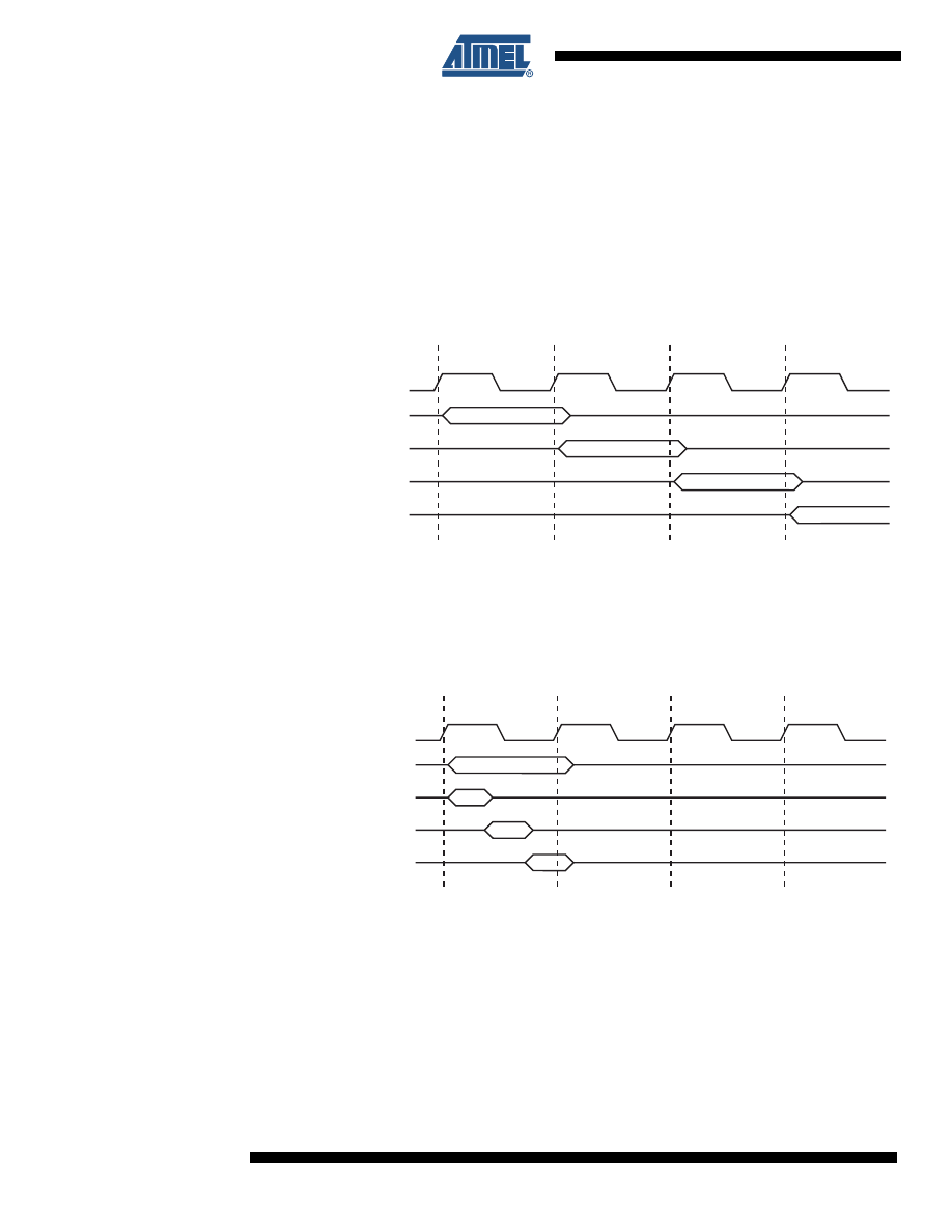
Instruction Execution Timing
This section describes the general access timing concepts for instruction execution. The AVR
CPU is driven by the CPU clock clk
CPU
, directly generated from the selected clock source for the
chip. No internal clock division is used.
shows the parallel instruction fetches and instruction executions enabled
by the Harvard architecture and the fast access Register File concept. This is the basic pipelin-
ing concept to obtain up to 1 MIPS per MHz with the corresponding unique results for functions
per cost, functions per clocks, and functions per power-unit.
Figure 4-4.
The Parallel Instruction Fetches and Instruction Executions
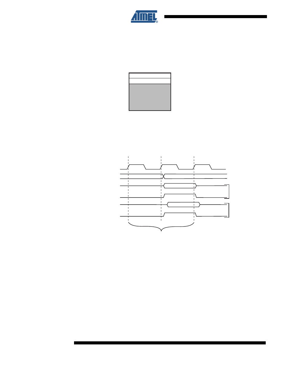
shows the internal timing concept for the Register File. In a single clock
cycle an ALU operation using two register operands is executed, and the result is stored back to
the destination register.
Figure 4-5.
Single Cycle ALU Operation
4.7
Reset and Interrupt Handling
The AVR provides several different interrupt sources. These interrupts and the separate Reset
Vector each have a separate Program Vector in the Program memory space. All interrupts are
assigned individual enable bits which must be written logic one together with the Global Interrupt
Enable bit in the Status Register in order to enable the interrupt.
The lowest addresses in the Program memory space are by default defined as the Reset and
Interrupt Vectors. The complete list of vectors is shown in
. The list also
determines the priority levels of the different interrupts. The lower the address the higher is the
clk
1st Instruction Fetch
1st Instruction Execute
2nd Instruction Fetch
2nd Instruction Execute
3rd Instruction Fetch
3rd Instruction Execute
4th Instruction Fetch
T1
T2
T3
T4
CPU
Total Execution Time
Register Operands Fetch
ALU Operation Execute
Result Write Back
T1
T2
T3
T4
clk
CPU

13
2535J–AVR–08/10
ATtiny13
priority level. RESET has the highest priority, and next is INT0 – the External Interrupt Request
0.
When an interrupt occurs, the Global Interrupt Enable I-bit is cleared and all interrupts are dis-
abled. The user software can write logic one to the I-bit to enable nested interrupts. All enabled
interrupts can then interrupt the current interrupt routine. The I-bit is automatically set when a
Return from Interrupt instruction – RETI – is executed.
There are basically two types of interrupts. The first type is triggered by an event that sets the
Interrupt Flag. For these interrupts, the Program Counter is vectored to the actual Interrupt Vec-
tor in order to execute the interrupt handling routine, and hardware clears the corresponding
Interrupt Flag. Interrupt Flags can also be cleared by writing a logic one to the flag bit position(s)
to be cleared. If an interrupt condition occurs while the corresponding interrupt enable bit is
cleared, the Interrupt Flag will be set and remembered until the interrupt is enabled, or the flag is
cleared by software. Similarly, if one or more interrupt conditions occur while the Global Interrupt
Enable bit is cleared, the corresponding Interrupt Flag(s) will be set and remembered until the
Global Interrupt Enable bit is set, and will then be executed by order of priority.
The second type of interrupts will trigger as long as the interrupt condition is present. These
interrupts do not necessarily have Interrupt Flags. If the interrupt condition disappears before the
interrupt is enabled, the interrupt will not be triggered.
When the AVR exits from an interrupt, it will always return to the main program and execute one
more instruction before any pending interrupt is served.
Note that the Status Register is not automatically stored when entering an interrupt routine, nor
restored when returning from an interrupt routine. This must be handled by software.
When using the CLI instruction to disable interrupts, the interrupts will be immediately disabled.
No interrupt will be executed after the CLI instruction, even if it occurs simultaneously with the
CLI instruction. The following example shows how this can be used to avoid interrupts during the
timed EEPROM write sequence..
Assembly Code Example
in
r16, SREG
; store SREG value
cli
; disable interrupts during timed sequence
sbi
EECR, EEMPE
; start EEPROM write
sbi
EECR, EEPE
out
SREG, r16
; restore SREG value (I-bit)
C Code Example
char
cSREG;
cSREG = SREG; /* store SREG value */
/* disable interrupts during timed sequence */
__disable_interrupt();
EECR |= (1<<EEMPE); /* start EEPROM write */
EECR |= (1<<EEPE);
SREG = cSREG; /* restore SREG value (I-bit) */

14
2535J–AVR–08/10
ATtiny13
When using the SEI instruction to enable interrupts, the instruction following SEI will be exe-
cuted before any pending interrupts, as shown in this example.
4.7.1
Interrupt Response Time
The interrupt execution response for all the enabled AVR interrupts is four clock cycles mini-
mum. After four clock cycles the Program Vector address for the actual interrupt handling routine
is executed. During this four clock cycle period, the Program Counter is pushed onto the Stack.
The vector is normally a jump to the interrupt routine, and this jump takes three clock cycles. If
an interrupt occurs during execution of a multi-cycle instruction, this instruction is completed
before the interrupt is served. If an interrupt occurs when the MCU is in sleep mode, the interrupt
execution response time is increased by four clock cycles. This increase comes in addition to the
start-up time from the selected sleep mode.
A return from an interrupt handling routine takes four clock cycles. During these four clock
cycles, the Program Counter (two bytes) is popped back from the Stack, the Stack Pointer is
incremented by two, and the I-bit in SREG is set.
Assembly Code Example
sei
; set Global Interrupt Enable
sleep
; enter sleep, waiting for interrupt
; note: will enter sleep before any pending
; interrupt(s)
C Code Example
__enable_interrupt(); /* set Global Interrupt Enable */
__sleep(); /* enter sleep, waiting for interrupt */
/* note: will enter sleep before any pending interrupt(s) */

15
2535J–AVR–08/10
ATtiny13
5. Memories
This section describes the different memories in the ATtiny13. The AVR architecture has two
main memory spaces, the Data memory and the Program memory space. In addition, the
ATtiny13 features an EEPROM Memory for data storage. All three memory spaces are linear
and regular.
5.1
In-System Reprogrammable Flash Program Memory
The ATtiny13 contains 1K byte On-chip In-System Reprogrammable Flash memory for program
storage. Since all AVR instructions are 16 or 32 bits wide, the Flash is organized as 512 x 16.
The Flash memory has an endurance of at least 10,000 write/erase cycles. The ATtiny13 Pro-
gram Counter (PC) is nine bits wide, thus addressing the 512 Program memory locations.
“Memory Programming” on page 102
contains a detailed description on Flash data serial down-
loading using the SPI pins.
Constant tables can be allocated within the entire Program memory address space (see the
LPM – Load Program memory instruction description).
Timing diagrams for instruction fetch and execution are presented in
Figure 5-1.
Program Memory Map
5.2
SRAM Data Memory
shows how the ATtiny13 SRAM Memory is organized.
The lower 160 Data memory locations address both the Register File, the I/O memory and the
internal data SRAM. The first 32 locations address the Register File, the next 64 locations the
standard I/O memory, and the last 64 locations address the internal data SRAM.
The five different addressing modes for the Data memory cover: Direct, Indirect with Displace-
ment, Indirect, Indirect with Pre-decrement, and Indirect with Post-increment. In the Register
File, registers R26 to R31 feature the indirect addressing pointer registers.
The direct addressing reaches the entire data space.
The Indirect with Displacement mode reaches 63 address locations from the base address given
by the Y- or Z-register.
When using register indirect addressing modes with automatic pre-decrement and post-incre-
ment, the address registers X, Y, and Z are decremented or incremented.
0x0000
0x01FF
Program Memory
16
2535J–AVR–08/10
ATtiny13
The 32 general purpose working registers, 64 I/O Registers, and the 64 bytes of internal data
SRAM in the ATtiny13 are all accessible through all these addressing modes. The Register File
is described in
“General Purpose Register File” on page 10
.
Figure 5-2.
Data Memory Map
5.2.1
Data Memory Access Times
This section describes the general access timing concepts for internal memory access. The
internal data SRAM access is performed in two clk
CPU
cycles as described in
.
Figure 5-3.
On-chip Data SRAM Access Cycles
5.3
EEPROM Data Memory
The ATtiny13 contains 64 bytes of data EEPROM memory. It is organized as a separate data
space, in which single bytes can be read and written. The EEPROM has an endurance of at
least 100,000 write/erase cycles. The access between the EEPROM and the CPU is described
in the following, specifying the EEPROM Address Registers, the EEPROM Data Register, and
the EEPROM Control Register. For a detailed description of Serial data downloading to the
EEPROM, see
5.3.1
EEPROM Read/Write Access
The EEPROM Access Registers are accessible in the I/O space.
32 Registers
64 I/O Registers
Internal SRAM
(64 x 8)
0x0000 - 0x001F
0x0020 - 0x005F
0x009F
0x0060
Data Memory
clk
WR
RD
Data
Data
Address
Address valid
T1
T2
T3
Compute Address
Read
Wr
ite
CPU
Memory Access Instruction
Next Instruction

17
2535J–AVR–08/10
ATtiny13
The write access times for the EEPROM are given in
tion, however, lets the user software detect when the next byte can be written. If the user code
contains instructions that write the EEPROM, some precautions must be taken. In heavily fil-
tered power supplies, V
CC
is likely to rise or fall slowly on Power-up/down. This causes the
device for some period of time to run at a voltage lower than specified as minimum for the clock
frequency used. See
“Preventing EEPROM Corruption” on page 19
problems in these situations.
In order to prevent unintentional EEPROM writes, a specific write procedure must be followed.
Refer to
“Atomic Byte Programming” on page 17
and
“Split Byte Programming” on page 17
details on this.
When the EEPROM is read, the CPU is halted for four clock cycles before the next instruction is
executed. When the EEPROM is written, the CPU is halted for two clock cycles before the next
instruction is executed.
5.3.2
Atomic Byte Programming
Using Atomic Byte Programming is the simplest mode. When writing a byte to the EEPROM, the
user must write the address into the EEARL Register and data into EEDR Register. If the
EEPMn bits are zero, writing EEPE (within four cycles after EEMPE is written) will trigger the
erase/write operation. Both the erase and write cycle are done in one operation and the total
programming time is given in
. The EEPE bit remains set until the erase
and write operations are completed. While the device is busy with programming, it is not possi-
ble to do any other EEPROM operations.
5.3.3
Split Byte Programming
It is possible to split the erase and write cycle in two different operations. This may be useful if
the system requires short access time for some limited period of time (typically if the power sup-
ply voltage falls). In order to take advantage of this method, it is required that the locations to be
written have been erased before the write operation. But since the erase and write operations
are split, it is possible to do the erase operations when the system allows doing time-critical
operations (typically after Power-up).
5.3.4
Erase
To erase a byte, the address must be written to EEARL. If the EEPMn bits are 0b01, writing the
EEPE (within four cycles after EEMPE is written) will trigger the erase operation only (program-
ming time is given in
). The EEPE bit remains set until the erase operation
completes. While the device is busy programming, it is not possible to do any other EEPROM
operations.
5.3.5
Write
To write a location, the user must write the address into EEARL and the data into EEDR. If the
EEPMn bits are 0b10, writing the EEPE (within four cycles after EEMPE is written) will trigger
the write operation only (programming time is given in
). The EEPE bit
remains set until the write operation completes. If the location to be written has not been erased
before write, the data that is stored must be considered as lost. While the device is busy with
programming, it is not possible to do any other EEPROM operations.
The calibrated Oscillator is used to time the EEPROM accesses. Make sure the Oscillator fre-
quency is within the requirements described in

18
2535J–AVR–08/10
ATtiny13
The following code examples show one assembly and one C function for erase, write, or atomic
write of the EEPROM. The examples assume that interrupts are controlled (e.g., by disabling
interrupts globally) so that no interrupts will occur during execution of these functions.
Assembly Code Example
EEPROM_write:
; Wait for completion of previous write
sbic
EECR,EEPE
rjmp
EEPROM_write
; Set Programming mode
ldi
r16, (0<<EEPM1)|(0<<EEPM0)
out
EECR, r16
; Set up address (r17) in address register
out
EEARL, r17
; Write data (r16) to data register
out
EEDR,r16
; Write logical one to EEMPE
sbi
EECR,EEMPE
; Start eeprom write by setting EEPE
sbi
EECR,EEPE
ret
C Code Example
void
EEPROM_write(unsigned char ucAddress, unsigned char ucData)
{
/* Wait for completion of previous write */
while(EECR & (1<<EEPE))
;
/* Set Programming mode */
EECR = (0<<EEPM1)|(0>>EEPM0)
/* Set up address and data registers */
EEARL = ucAddress;
EEDR = ucData;
/* Write logical one to EEMPE */
EECR |= (1<<EEMPE);
/* Start eeprom write by setting EEPE */
EECR |= (1<<EEPE);
}

19
2535J–AVR–08/10
ATtiny13
The next code examples show assembly and C functions for reading the EEPROM. The exam-
ples assume that interrupts are controlled so that no interrupts will occur during execution of
these functions.
5.3.6
Preventing EEPROM Corruption
During periods of low V
CC
, the EEPROM data can be corrupted because the supply voltage is
too low for the CPU and the EEPROM to operate properly. These issues are the same as for
board level systems using EEPROM, and the same design solutions should be applied.
An EEPROM data corruption can be caused by two situations when the voltage is too low. First,
a regular write sequence to the EEPROM requires a minimum voltage to operate correctly. Sec-
ondly, the CPU itself can execute instructions incorrectly, if the supply voltage is too low.
EEPROM data corruption can easily be avoided by following this design recommendation:
Keep the AVR RESET active (low) during periods of insufficient power supply voltage. This can
be done by enabling the internal Brown-out Detector (BOD). If the detection level of the internal
BOD does not match the needed detection level, an external low V
CC
reset protection circuit can
be used. If a reset occurs while a write operation is in progress, the write operation will be com-
pleted provided that the power supply voltage is sufficient.
Assembly Code Example
EEPROM_read:
; Wait for completion of previous write
sbic
EECR,EEPE
rjmp
EEPROM_read
; Set up address (r17) in address register
out
EEARL, r17
; Start eeprom read by writing EERE
sbi
EECR,EERE
; Read data from data register
in
r16,EEDR
ret
C Code Example
unsigned char
EEPROM_read(unsigned char ucAddress)
{
/* Wait for completion of previous write */
while(EECR & (1<<EEPE))
;
/* Set up address register */
EEARL = ucAddress;
/* Start eeprom read by writing EERE */
EECR |= (1<<EERE);
/* Return data from data register */
return EEDR;
}

20
2535J–AVR–08/10
ATtiny13
5.4
I/O Memory
The I/O space definition of the ATtiny13 is shown in
“Register Summary” on page 156
All ATtiny13 I/Os and peripherals are placed in the I/O space. All I/O locations may be accessed
by the LD/LDS/LDD and ST/STS/STD instructions, transferring data between the 32 general
purpose working registers and the I/O space. I/O Registers within the address range 0x00 -
0x1F are directly bit-accessible using the SBI and CBI instructions. In these registers, the value
of single bits can be checked by using the SBIS and SBIC instructions. Refer to the instruction
set section for more details. When using the I/O specific commands IN and OUT, the I/O
addresses 0x00 - 0x3F must be used. When addressing I/O Registers as data space using LD
and ST instructions, 0x20 must be added to these addresses.
For compatibility with future devices, reserved bits should be written to zero if accessed.
Reserved I/O memory addresses should never be written.
Some of the Status Flags are cleared by writing a logical one to them. Note that, unlike most
other AVRs, the CBI and SBI instructions will only operate on the specified bit, and can therefore
be used on registers containing such Status Flags. The CBI and SBI instructions work with reg-
isters 0x00 to 0x1F only.
The I/O and Peripherals Control Registers are explained in later sections.
5.5
Register Description
5.5.1
EEARL – EEPROM Address Register
• Bits 7:6 – Res: Reserved Bits
These bits are reserved bits in the ATtiny13 and will always read as zero.
• Bits 5:0 – EEAR[5:0]: EEPROM Address
The EEPROM Address Register – EEARL – specifies the EEPROM address in the 64 bytes
EEPROM space. The EEPROM data bytes are addressed linearly between 0 and 63. The initial
value of EEARL is undefined. A proper value must be written before the EEPROM may be
accessed.
5.5.2
EEDR – EEPROM Data Register
• Bits 7:0 – EEDR7:0: EEPROM Data
For the EEPROM write operation the EEDR Register contains the data to be written to the
EEPROM in the address given by the EEARL Register. For the EEPROM read operation, the
EEDR contains the data read out from the EEPROM at the address given by EEARL.
Bit
7
6
5
4
3
2
1
0
–
–
EEAR5
EEAR4
EEAR3
EEAR2
EEAR1
EEAR0
EEARL
Read/Write
R
R
R/W
R/W
R/W
R/W
R/W
R/W
Initial Value
0
0
X
X
X
X
X
X
Bit
7
6
5
4
3
2
1
0
EEDR7
EEDR6
EEDR5
EEDR4
EEDR3
EEDR2
EEDR1
EEDR0
EEDR
Read/Write
R/W
R/W
R/W
R/W
R/W
R/W
R/W
R/W
Initial Value
X
X
X
X
X
X
X
X

21
2535J–AVR–08/10
ATtiny13
5.5.3
EECR – EEPROM Control Register
• Bit 7 – Res: Reserved Bit
This bit is reserved for future use and will always read as 0 in ATtiny13. For compatibility with
future AVR devices, always write this bit to zero. After reading, mask out this bit.
• Bit 6 – Res: Reserved Bit
This bit is reserved in the ATtiny13 and will always read as zero.
• Bits 5:4 – EEPM[1:0]: EEPROM Programming Mode Bits
The EEPROM Programming mode bits setting defines which programming action that will be
triggered when writing EEPE. It is possible to program data in one atomic operation (erase the
old value and program the new value) or to split the Erase and Write operations in two different
operations. The Programming times for the different modes are shown in
While EEPE is set, any write to EEPMn will be ignored. During reset, the EEPMn bits will be
reset to 0b00 unless the EEPROM is busy programming.
• Bit 3 – EERIE: EEPROM Ready Interrupt Enable
Writing EERIE to one enables the EEPROM Ready Interrupt if the I-bit in SREG is set. Writing
EERIE to zero disables the interrupt. The EEPROM Ready Interrupt generates a constant inter-
rupt when Non-volatile memory is ready for programming.
• Bit 2 – EEMPE: EEPROM Master Program Enable
The EEMPE bit determines whether writing EEPE to one will have effect or not.
When EEMPE is set, setting EEPE within four clock cycles will program the EEPROM at the
selected address. If EEMPE is zero, setting EEPE will have no effect. When EEMPE has been
written to one by software, hardware clears the bit to zero after four clock cycles.
• Bit 1 – EEPE: EEPROM Program Enable
The EEPROM Program Enable Signal EEPE is the programming enable signal to the EEPROM.
When EEPE is written, the EEPROM will be programmed according to the EEPMn bits setting.
The EEMPE bit must be written to one before a logical one is written to EEPE, otherwise no
EEPROM write takes place. When the write access time has elapsed, the EEPE bit is cleared by
hardware. When EEPE has been set, the CPU is halted for two cycles before the next instruction
is executed.
Bit
7
6
5
4
3
2
1
0
–
–
EEPM1
EEPM0
EERIE
EEMPE
EEPE
EERE
EECR
Read/Write
R
R
R/W
R/W
R/W
R/W
R/W
R/W
Initial Value
0
0
X
X
0
0
X
0
Table 5-1.
EEPROM Mode Bits
EEPM1
EEPM0
Programming
Time
Operation
0
0
3.4 ms
Erase and Write in one operation (Atomic Operation)
0
1
1.8 ms
Erase Only
1
0
1.8 ms
Write Only
1
1
–
Reserved for future use

22
2535J–AVR–08/10
ATtiny13
• Bit 0 – EERE: EEPROM Read Enable
The EEPROM Read Enable Signal – EERE – is the read strobe to the EEPROM. When the cor-
rect address is set up in the EEARL Register, the EERE bit must be written to one to trigger the
EEPROM read. The EEPROM read access takes one instruction, and the requested data is
available immediately. When the EEPROM is read, the CPU is halted for four cycles before the
next instruction is executed. The user should poll the EEPE bit before starting the read opera-
tion. If a write operation is in progress, it is neither possible to read the EEPROM, nor to change
the EEARL Register.
23
2535J–AVR–08/10
ATtiny13
6. System Clock and Clock Options
6.1
Clock Systems and their Distribution
presents the principal clock systems in the AVR and their distribution. All of the clocks
need not be active at a given time. In order to reduce power consumption, the clocks to modules
not being used can be halted by using different sleep modes, as described in
ment and Sleep Modes” on page 30
. The clock systems are detailed below.
Figure 6-1.
Clock Distribution
6.1.1
CPU Clock – clk
CPU
The CPU clock is routed to parts of the system concerned with operation of the AVR core.
Examples of such modules are the General Purpose Register File, the Status Register and the
Data memory holding the Stack Pointer. Halting the CPU clock inhibits the core from performing
general operations and calculations.
6.1.2
I/O Clock – clk
I/O
The I/O clock is used by the majority of the I/O modules, like Timer/Counter. The I/O clock is
also used by the External Interrupt module, but note that some external interrupts are detected
by asynchronous logic, allowing such interrupts to be detected even if the I/O clock is halted.
6.1.3
Flash Clock – clk
FLASH
The Flash clock controls operation of the Flash interface. The Flash clock is usually active simul-
taneously with the CPU clock.
General I/O
Modules
CPU Core
RAM
clk
I/O
AVR Clock
Control Unit
clk
CPU
Flash and
EEPROM
clk
FLASH
Source clock
Watchdog Timer
Watchdog
Oscillator
Reset Logic
Clock
Multiplexer
Watchdog clock
Calibrated RC
Oscillator
External Clock
ADC
clk
ADC
24
2535J–AVR–08/10
ATtiny13
6.1.4
ADC Clock – clk
ADC
The ADC is provided with a dedicated clock domain. This allows halting the CPU and I/O clocks
in order to reduce noise generated by digital circuitry. This gives more accurate ADC conversion
results.
6.2
Clock Sources
The device has the following clock source options, selectable by Flash fuse bits as shown
below. The clock from the selected source is input to the AVR clock generator, and routed to the
appropriate modules.
Note:
1. For all fuses “1” means unprogrammed while “0” means programmed.
The various choices for each clocking option is given in the following sections. When the CPU
wakes up from Power-down or Power-save, the selected clock source is used to time the start-
up, ensuring stable Oscillator operation before instruction execution starts. When the CPU starts
from reset, there is an additional delay allowing the power to reach a stable level before com-
mencing normal operation. The Watchdog Oscillator is used for timing this real-time part of the
start-up time. The number of WDT Oscillator cycles used for each time-out is shown in
6.2.1
External Clock
To drive the device from an external clock source, CLKI should be driven as shown in
. To run the device on an external clock, the CKSEL fuses must be programmed to “00”.
Figure 6-2.
External Clock Drive Configuration
Table 6-1.
Device Clocking Options Select
Device Clocking Option
External Clock (see
00
Calibrated Internal 4.8/9.6 MHz Oscillator (see
)
01, 10
Internal 128 kHz Oscillator (see
)
11
Table 6-2.
Number of Watchdog Oscillator Cycles
Typ Time-out
Number of Cycles
4 ms
512
64 ms
8K (8,192)
EXTERNAL
CLOCK
SIGNAL
CLKI
GND
25
2535J–AVR–08/10
ATtiny13
When this clock source is selected, start-up times are determined by the SUT fuses as shown in
When applying an external clock, it is required to avoid sudden changes in the applied clock fre-
quency to ensure stable operation of the MCU. A variation in frequency of more than 2% from
one clock cycle to the next can lead to unpredictable behavior. It is required to ensure that the
MCU is kept in Reset during such changes in the clock frequency.
Note that the System Clock Prescaler can be used to implement run-time changes of the internal
clock frequency while still ensuring stable operation. Refer to
“System Clock Prescaler” on page
for details.
6.2.2
Calibrated Internal 4.8/9.6 MHz Oscillator
The calibrated internal oscillator provides a 4.8 or 9.6 MHz clock source. The frequency is nomi-
nal at 3V and 25
°C. If the frequency exceeds the specification of the device (depends on V
CC
),
the CKDIV8 fuse must be programmed so that the internal clock is divided by 8 during start-up.
See “System Clock Prescaler” on page 26.
The internal oscillator is selected as the system clock by programming the CKSEL fuses as
shown in
. If selected, it will operate with no external components.
Note:
1. The device is shipped with this option selected.
During reset, hardware loads the calibration data into the OSCCAL register and thereby auto-
matically calibrates the oscillator. There are separate calibration bytes for 4.8 and 9.6 MHz
operation but only one is automatically loaded during reset (see section
). This is because the only difference between 4.8 MHz and 9.6 MHz mode is an inter-
nal clock divider.
By changing the OSCCAL register from SW, see
“OSCCAL – Oscillator Calibration Register” on
, it is possible to get a higher calibration accuracy than by using the factory calibration.
“Calibrated Internal RC Oscillator Accuracy” on page 118
When this oscillator is used as the chip clock, the Watchdog Oscillator will still be used for the
Watchdog Timer and for the Reset Time-out. For more information on the pre-programmed cali-
bration value, see the section
“Calibration Bytes” on page 104
Table 6-3.
Start-up Times for the External Clock Selection
SUT1..0
Start-up Time from
Power-down and Power-save
Additional Delay
from Reset
Recommended
Usage
00
6 CK
14CK
BOD enabled
01
6 CK
14CK + 4 ms
Fast rising power
10
6 CK
14CK + 64 ms
Slowly rising power
11
Reserved
Table 6-4.
Internal Calibrated RC Oscillator Operating Modes
CKSEL1..0
Nominal Frequency
10
9.6 MHz
01
4.8 MHz

26
2535J–AVR–08/10
ATtiny13
When this Oscillator is selected, start-up times are determined by the SUT fuses as shown in
Note:
1. The device is shipped with this option selected.
6.2.3
Internal 128 kHz Oscillator
The 128 kHz internal Oscillator is a low power Oscillator providing a clock of 128 kHz. The fre-
quency depends on supply voltage, temperature and batch variations. This clock may be select
as the system clock by programming the CKSEL fuses to “11”.
When this clock source is selected, start-up times are determined by the SUT fuses as shown in
6.2.4
Default Clock Source
The device is shipped with CKSEL = “10”, SUT = “10”, and CKDIV8 programmed. The default
clock source setting is therefore the Internal RC Oscillator running at 9.6 MHz with longest start-
up time and an initial system clock prescaling of 8. This default setting ensures that all users can
make their desired clock source setting using an In-System or High-voltage Programmer.
6.3
System Clock Prescaler
The ATtiny13 system clock can be divided by setting the
“CLKPR – Clock Prescale Register” on
. This feature can be used to decrease power consumption when the requirement for
processing power is low. This can be used with all clock source options, and it will affect the
clock frequency of the CPU and all synchronous peripherals. clk
I/O
, clk
ADC
, clk
CPU
, and clk
FLASH
are divided by a factor as shown in
.
6.3.1
Switching Time
When switching between prescaler settings, the System Clock Prescaler ensures that no
glitches occur in the clock system and that no intermediate frequency is higher than neither the
clock frequency corresponding to the previous setting, nor the clock frequency corresponding to
the new setting.
Table 6-5.
Start-up Times for the Internal Calibrated RC Oscillator Clock Selection
SUT1..0
Start-up Time
from Power-down
Additional Delay from
Reset (V
CC
= 5.0V)
Recommended Usage
00
6 CK
14CK
BOD enabled
01
6 CK
14CK + 4 ms
Fast rising power
6 CK
14CK + 64 ms
Slowly rising power
11
Reserved
Table 6-6.
Start-up Times for the 128 kHz Internal Oscillator
SUT1:0
Start-up Time from
Power-down and Power-save
Additional Delay
from Reset
Recommended
Usage
00
6 CK
14CK
BOD enabled
01
6 CK
14CK + 4 ms
Fast rising power
10
6 CK
14CK + 64 ms
Slowly rising power
11
Reserved
27
2535J–AVR–08/10
ATtiny13
The ripple counter that implements the prescaler runs at the frequency of the undivided clock,
which may be faster than the CPU’s clock frequency. Hence, it is not possible to determine the
state of the prescaler – even if it were readable, and the exact time it takes to switch from one
clock division to another cannot be exactly predicted.
From the time the CLKPS values are written, it takes between T1 + T2 and T1 + 2*T2 before the
new clock frequency is active. In this interval, 2 active clock edges are produced. Here, T1 is the
previous clock period, and T2 is the period corresponding to the new prescaler setting.
6.4
Register Description
6.4.1
OSCCAL – Oscillator Calibration Register
• Bit 7 – Res: Reserved Bit
This bit is reserved bit in ATtiny13 and it will always read zero.
• Bits 6:0 – CAL[6:0]: Oscillator Calibration Value
Writing the calibration byte to this address will trim the internal Oscillator to remove process vari-
ations from the Oscillator frequency. This is done automatically during Chip Reset. When
OSCCAL is zero, the lowest available frequency is chosen. Writing non-zero values to this regis-
ter will increase the frequency of the internal Oscillator. Writing 0x7F to the register gives the
highest available frequency.
The calibrated Oscillator is used to time EEPROM and Flash access. If EEPROM or Flash is
written, do not calibrate to more than 10% above the nominal frequency. Otherwise, the
EEPROM or Flash write may fail. Note that the Oscillator is intended for calibration to 9.6 MHz or
4.8 MHz. Tuning to other values is not guaranteed, as indicated in
To ensure stable operation of the MCU the calibration value should be changed in small steps. A
variation in frequency of more than 2% from one cycle to the next can lead to unpredicatble
behavior. Changes in OSCCAL should not exceed 0x20 for each calibration. It is required to
ensure that the MCU is kept in Reset during such changes in the clock frequency
Bit
7
6
5
4
3
2
1
0
–
CAL6
CAL5
CAL4
CAL3
CAL2
CAL1
CAL0
OSCCAL
Read/Write
R
R/W
R/W
R/W
R/W
R/W
R/W
R/W
Initial Value
0
Device Specific Calibration Value
Table 6-7.
Internal RC Oscillator Frequency Range
OSCCAL Value
Typical Lowest Frequency
with Respect to Nominal Frequency
Typical Highest Frequency
with Respect to Nominal Frequency
0x00
50%
100%
0x3F
75%
150%
0x7F
100%
200%

28
2535J–AVR–08/10
ATtiny13
6.4.2
CLKPR – Clock Prescale Register
• Bit 7 – CLKPCE: Clock Prescaler Change Enable
The CLKPCE bit must be written to logic one to enable change of the CLKPS bits. The CLKPCE
bit is only updated when the other bits in CLKPR are simultaneously written to zero. CLKPCE is
cleared by hardware four cycles after it is written or when the CLKPS bits are written. Rewriting
the CLKPCE bit within this time-out period does neither extend the time-out period, nor clear the
CLKPCE bit.
• Bits 6:4 – Res: Reserved Bits
These bits are reserved bits in the ATtiny13 and will always read as zero.
• Bits 3:0 – CLKPS3:0: Clock Prescaler Select Bits 3 - 0
These bits define the division factor between the selected clock source and the internal system
clock. These bits can be written run-time to vary the clock frequency to suit the application
requirements. As the divider divides the master clock input to the MCU, the speed of all synchro-
nous peripherals is reduced when a division factor is used. The division factors are given in
.
To avoid unintentional changes of clock frequency, a special write procedure must be followed
to change the CLKPS bits:
1. Write the Clock Prescaler Change Enable (CLKPCE) bit to one and all other bits in
CLKPR to zero.
2. Within four cycles, write the desired value to CLKPS while writing a zero to CLKPCE.
Interrupts must be disabled when changing prescaler setting to make sure the write procedure is
not interrupted.hee setting. The Application software must ensure that a sufficient division factor
is chosen if the selected clock source has a higher frequency than the maximum frequency of
the device at the present operating conditions. The device is shipped with the CKDIV8 fuse
programmed.
Bit
7
6
5
4
3
2
1
0
CLKPCE
–
–
–
CLKPS3
CLKPS2
CLKPS1
CLKPS0
CLKPR
Read/Write
R/W
R
R
R
R/W
R/W
R/W
R/W
Initial Value
0
0
0
0
See Bit Description
Table 6-8.
Clock Prescaler Select
CLKPS3
CLKPS2
CLKPS1
CLKPS0
Clock Division Factor
0
0
0
0
1
0
0
0
1
2
0
0
1
0
4
0
0
1
1
8
0
1
0
0
16
0
1
0
1
32
0
1
1
0
64
0
1
1
1
128
1
0
0
0
256

29
2535J–AVR–08/10
ATtiny13
1
0
0
1
Reserved
1
0
1
0
Reserved
1
0
1
1
Reserved
1
1
0
0
Reserved
1
1
0
1
Reserved
1
1
1
0
Reserved
1
1
1
1
Reserved
Table 6-8.
Clock Prescaler Select (Continued)
CLKPS3
CLKPS2
CLKPS1
CLKPS0
Clock Division Factor

30
2535J–AVR–08/10
ATtiny13
7. Power Management and Sleep Modes
The high performance and industry leading code efficiency makes the AVR microcontrollers an
ideal choise for low power applications. In addition, sleep modes enable the application to shut
down unused modules in the MCU, thereby saving power. The AVR provides various sleep
modes allowing the user to tailor the power consumption to the application’s requirements.
7.1
Sleep Modes
presents the different clock systems in the ATtiny13, and their distribu-
tion. The figure is helpful in selecting an appropriate sleep mode.
shows the different
sleep modes and their wake up sources.
Note:
1. For INT0, only level interrupt.
To enter any of the three sleep modes, the SE bit in MCUCR must be written to logic one and a
SLEEP instruction must be executed. The SM1..0 bits in the MCUCR Register select which
sleep mode (Idle, ADC Noise Reduction, or Power-down) will be activated by the SLEEP instruc-
tion. See
for a summary.
If an enabled interrupt occurs while the MCU is in a sleep mode, the MCU wakes up. The MCU
is then halted for four cycles in addition to the start-up time, executes the interrupt routine, and
resumes execution from the instruction following SLEEP. The contents of the Register File and
SRAM are unaltered when the device wakes up from sleep. If a reset occurs during sleep mode,
the MCU wakes up and executes from the Reset Vector.
Note that if a level triggered interrupt is used for wake-up from Power-down mode, the changed
level must be held for some time to wake up the MCU. Refer to
“External Interrupts” on page 45
for details.
7.1.1
Idle Mode
When the SM[1:0] bits are written to 00, the SLEEP instruction makes the MCU enter Idle mode,
stopping the CPU but allowing Analog Comparator, ADC, Timer/Counter, Watchdog, and the
interrupt system to continue operating. This sleep mode basically halts clk
CPU
and clk
FLASH
, while
allowing the other clocks to run.
Idle mode enables the MCU to wake up from external triggered interrupts as well as internal
ones like the Timer Overflow. If wake-up from the Analog Comparator interrupt is not required,
the Analog Comparator can be powered down by setting the ACD bit in the Analog Comparator
Table 7-1.
Active Clock Domains and Wake-up Sources in the Different Sleep Modes
Active Clock Domains
Oscillators
Wake-up Sources
Sleep Mode
clk
CPU
clk
FL
AS
H
clk
IO
clk
ADC
Mai
n Clock
So
urce Enabl
ed
INT0 and
Pi
n C
han
ge
SPM/
EEPROM
R
eady
ADC
Other I/O
W
a
tchd
og
Interrupt
Idle
X
X
X
X
X
X
X
X
ADC Noise
Reduction
X
X
X
X
X
X
Power-down
X
X

31
2535J–AVR–08/10
ATtiny13
Control and Status Register – ACSR. This will reduce power consumption in Idle mode. If the
ADC is enabled, a conversion starts automatically when this mode is entered.
7.1.2
ADC Noise Reduction Mode
When the SM[1:0] bits are written to 01, the SLEEP instruction makes the MCU enter ADC
Noise Reduction mode, stopping the CPU but allowing the ADC, the external interrupts, and the
Watchdog to continue operating (if enabled). This sleep mode halts clk
I/O
, clk
CPU
, and clk
FLASH
,
while allowing the other clocks to run.
This improves the noise environment for the ADC, enabling higher resolution measurements. If
the ADC is enabled, a conversion starts automatically when this mode is entered. Apart form the
ADC Conversion Complete interrupt, only an External Reset, a Watchdog Reset, a Brown-out
Reset, an SPM/EEPROM ready interrupt, an external level interrupt on INT0 or a pin change
interrupt can wake up the MCU from ADC Noise Reduction mode.
7.1.3
Power-down Mode
When the SM[1:0] bits are written to 10, the SLEEP instruction makes the MCU enter Power-
down mode. In this mode, the Oscillator is stopped, while the external interrupts, and the Watch-
dog continue operating (if enabled). Only an External Reset, a Watchdog Reset, a Brown-out
Reset, an external level interrupt on INT0, or a pin change interrupt can wake up the MCU. This
sleep mode halts all generated clocks, allowing operation of asynchronous modules only.
7.2
Minimizing Power Consumption
There are several issues to consider when trying to minimize the power consumption in an AVR
controlled system. In general, sleep modes should be used as much as possible, and the sleep
mode should be selected so that as few as possible of the device’s functions are operating. All
functions not needed should be disabled. In particular, the following modules may need special
consideration when trying to achieve the lowest possible power consumption.
7.2.1
Analog to Digital Converter
If enabled, the ADC will be enabled in all sleep modes. To save power, the ADC should be dis-
abled before entering any sleep mode. When the ADC is turned off and on again, the next
conversion will be an extended conversion. Refer to
“Analog to Digital Converter” on page 81
details on ADC operation.
7.2.2
Analog Comparator
When entering Idle mode, the Analog Comparator should be disabled if not used. When entering
ADC Noise Reduction mode, the Analog Comparator should be disabled. In the other sleep
modes, the Analog Comparator is automatically disabled. However, if the Analog Comparator is
set up to use the Internal Voltage Reference as input, the Analog Comparator should be dis-
abled in all sleep modes. Otherwise, the Internal Voltage Reference will be enabled,
independent of sleep mode. Refer to
“Analog Comparator” on page 78
for details on how to con-
figure the Analog Comparator.
7.2.3
Brown-out Detector
If the Brown-out Detector is not needed in the application, this module should be turned off. If the
Brown-out Detector is enabled by the BODLEVEL fuses, it will be enabled in all sleep modes,
and hence, always consume power. In the deeper sleep modes, this will contribute significantly
to the total current consumption. Refer to
“Brown-out Detection” on page 36
for details on how to
configure the Brown-out Detector.

32
2535J–AVR–08/10
ATtiny13
7.2.4
Internal Voltage Reference
The Internal Voltage Reference will be enabled when needed by the Brown-out Detection, the
Analog Comparator or the ADC. If these modules are disabled as described in the sections
above, the internal voltage reference will be disabled and it will not be consuming power. When
turned on again, the user must allow the reference to start up before the output is used. If the
reference is kept on in sleep mode, the output can be used immediately. Refer to
for details on the start-up time.
7.2.5
Watchdog Timer
If the Watchdog Timer is not needed in the application, this module should be turned off. If the
Watchdog Timer is enabled, it will be enabled in all sleep modes, and hence, always consume
power. In the deeper sleep modes, this will contribute significantly to the total current consump-
tion. Refer to
for details on how to configure the Watchdog Timer.
7.2.6
Port Pins
When entering a sleep mode, all port pins should be configured to use minimum power. The
most important thing is then to ensure that no pins drive resistive loads. In sleep modes where
both the I/O clock (clk
I/O
) and the ADC clock (clk
ADC
) are stopped, the input buffers of the device
will be disabled. This ensures that no power is consumed by the input logic when not needed. In
some cases, the input logic is needed for detecting wake-up conditions, and it will then be
enabled. Refer to the section
“Digital Input Enable and Sleep Modes” on page 52
for details on
which pins are enabled. If the input buffer is enabled and the input signal is left floating or has an
analog signal level close to V
CC
/2, the input buffer will use excessive power.
For analog input pins, the digital input buffer should be disabled at all times. An analog signal
level close to V
CC
/2 on an input pin can cause significant current even in active mode. Digital
input buffers can be disabled by writing to the Digital Input Disable Register (DIDR0). Refer to
“DIDR0 – Digital Input Disable Register 0” on page 80
for details.
7.3
Register Description
7.3.1
MCUCR – MCU Control Register
The MCU Control Register contains control bits for power management.
• Bit 5 – SE: Sleep Enable
The SE bit must be written to logic one to make the MCU enter the sleep mode when the SLEEP
instruction is executed. To avoid the MCU entering the sleep mode unless it is the programmer’s
purpose, it is recommended to write the Sleep Enable (SE) bit to one just before the execution of
the SLEEP instruction and to clear it immediately after waking up.
Bit
7
6
5
4
3
2
1
0
–
PUD
SE
SM1
SM0
—
ISC01
ISC00
MCUCR
Read/Write
R
R/W
R/W
R/W
R/W
R
R/W
R/W
Initial Value
0
0
0
0
0
0
0
0

33
2535J–AVR–08/10
ATtiny13
• Bits 4:3 – SM[1:0]: Sleep Mode Select Bits 1:0
These bits select between the three available sleep modes as shown in
• Bit 2 – Res: Reserved Bit
This bit is a reserved bit in the ATtiny13 and will always read as zero.
Table 7-2.
Sleep Mode Select
SM1
SM0
Sleep Mode
0
0
Idle
0
1
ADC Noise Reduction
1
0
Power-down
1
1
Reserved
34
2535J–AVR–08/10
ATtiny13
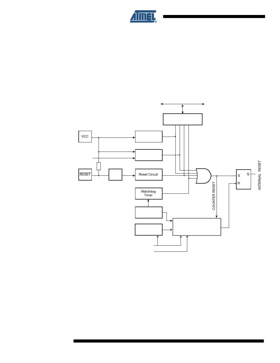
8. System Control and Reset
8.0.1
Resetting the AVR
During reset, all I/O Registers are set to their initial values, and the program starts execution
from the Reset Vector. The instruction placed at the Reset Vector must be a RJMP – Relative
Jump – instruction to the reset handling routine. If the program never enables an interrupt
source, the Interrupt Vectors are not used, and regular program code can be placed at these
locations. The circuit diagram in
shows the reset logic.
Reset Characteristics” on page 119
defines the electrical parameters of the reset circuitry.
Figure 8-1.
Reset Logic
The I/O ports of the AVR are immediately reset to their initial state when a reset source goes
active. This does not require any clock source to be running.
After all reset sources have gone inactive, a delay counter is invoked, stretching the internal
reset. This allows the power to reach a stable level before normal operation starts. The time-out
period of the delay counter is defined by the user through the SUT and CKSEL fuses. The differ-
ent selections for the delay period are presented in
.
MCU Status
Register (MCUSR)
Brown-out
Reset Circuit
BODLEVEL [1..0]
Delay Counters
CKSEL[1:0]
CK
TIMEOUT
WDRF
BORF
EXTRF
PORF
DATA BUS
Clock
Generator
SPIKE
FILTER
Pull-up Resistor
Watchdog
Oscillator
SUT[1:0]
Power-on Reset
Circuit
35
2535J–AVR–08/10
ATtiny13
8.1
Reset Sources
The ATtiny13 has four sources of reset:
• Power-on Reset. The MCU is reset when the supply voltage is below the Power-on Reset
threshold (V
POT
).
• External Reset. The MCU is reset when a low level is present on the RESET pin for longer
than the minimum pulse length.
• Watchdog Reset. The MCU is reset when the Watchdog Timer period expires and the
Watchdog is enabled.
• Brown-out Reset. The MCU is reset when the supply voltage V
CC
is below the Brown-out
Reset threshold (V
BOT
) and the Brown-out Detector is enabled.
8.1.1
Power-on Reset
A Power-on Reset (POR) pulse is generated by an On-chip detection circuit. The detection level
is defined in
“System and Reset Characteristics” on page 119
. The POR is activated whenever
V
CC
is below the detection level. The POR circuit can be used to trigger the Start-up Reset, as
well as to detect a failure in supply voltage.
A Power-on Reset (POR) circuit ensures that the device is reset from Power-on. Reaching the
Power-on Reset threshold voltage invokes the delay counter, which determines how long the
device is kept in RESET after V
CC
rise. The RESET signal is activated again, without any delay,
when V
CC
decreases below the detection level.
Figure 8-2.
MCU Start-up, RESET Tied to V
CC
Figure 8-3.
MCU Start-up, RESET Extended Externally
V
RESET
TIME-OUT
INTERNAL
RESET
t
TOUT
V
POT
V
RST
CC
RESET
TIME-OUT
INTERNAL
RESET
t
TOUT
V
POT
V
RST
V
CC
36
2535J–AVR–08/10
ATtiny13
8.1.2
External Reset
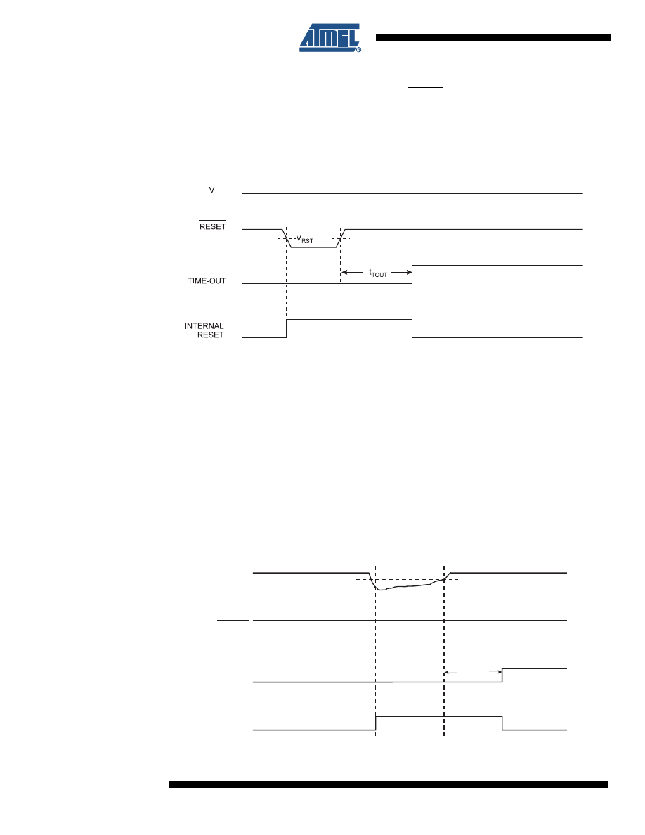
An External Reset is generated by a low level on the RESET pin if enabled. Reset pulses longer
than the minimum pulse width (
See “System and Reset Characteristics” on page 119.
) will gen-
erate a reset, even if the clock is not running. Shorter pulses are not guaranteed to generate a
reset. When the applied signal reaches the Reset Threshold Voltage – V
RST
– on its positive
edge, the delay counter starts the MCU after the Time-out period – t
TOUT
–
has expired.
Figure 8-4.
External Reset During Operation
8.1.3
Brown-out Detection
ATtiny13 has an On-chip Brown-out Detection (BOD) circuit for monitoring the V
CC
level during
operation by comparing it to a fixed trigger level. The trigger level for the BOD can be selected
by the BODLEVEL fuses. The trigger level has a hysteresis to ensure spike free Brown-out
Detection. The hysteresis on the detection level should be interpreted as V
BOT+
= V
BOT
+ V
HYST
/2
and V
BOT-
= V
BOT
- V
HYST
/2.
When the BOD is enabled, and V
CC
decreases to a value below the trigger level (V
BOT-
in
), the Brown-out Reset is immediately activated. When V
CC
increases above the
trigger level (V
BOT+
in
), the delay counter starts the MCU after the Time-
out period t
TOUT
has expired.
The BOD circuit will only detect a drop in V
CC
if the voltage stays below the trigger level for lon-
ger than t
BOD
given in
“System and Reset Characteristics” on page 119
Figure 8-5.
Brown-out Reset During Operation
CC
V
CC
RESET
TIME-OUT
INTERNAL
RESET
V
BOT-
V
BOT+
t
TOUT
37
2535J–AVR–08/10
ATtiny13
8.1.4
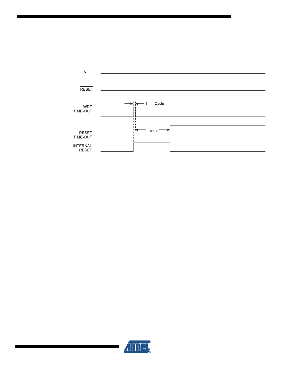
Watchdog Reset
When the Watchdog times out, it will generate a short reset pulse of one CK cycle duration. On
the falling edge of this pulse, the delay timer starts counting the Time-out period t
TOUT
. Refer to
for details on operation of the Watchdog Timer.
Figure 8-6.
Watchdog Reset During Operation
8.2
Internal Voltage Reference
ATtiny13 features an internal bandgap reference. This reference is used for Brown-out Detec-
tion, and it can be used as an input to the Analog Comparator or the ADC.
8.2.1
Voltage Reference Enable Signals and Start-up Time
The voltage reference has a start-up time that may influence the way it should be used. The
start-up time is given in
“System and Reset Characteristics” on page 119
. To save power, the
reference is not always turned on. The reference is on during the following situations:
• When the BOD is enabled (by programming the BODLEVEL [1..0] fuse).
• When the bandgap reference is connected to the Analog Comparator (by setting the ACBG
bit in ACSR).
• When the ADC is enabled.
Thus, when the BOD is not enabled, after setting the ACBG bit or enabling the ADC, the user
must always allow the reference to start up before the output from the Analog Comparator or
ADC is used. To reduce power consumption in Power-down mode, the user can avoid the three
conditions above to ensure that the reference is turned off before entering Power-down mode.
8.3
Watchdog Timer
ATtiny13 has an Enhanced Watchdog Timer (WDT). The WDT is a timer counting cycles of a
separate on-chip 128 kHz oscillator. The WDT gives an interrupt or a system reset when the
counter reaches a given time-out value. In normal operation mode, it is required that the system
uses the WDR - Watchdog Timer Reset - instruction to restart the counter before the time-out
CK
CC
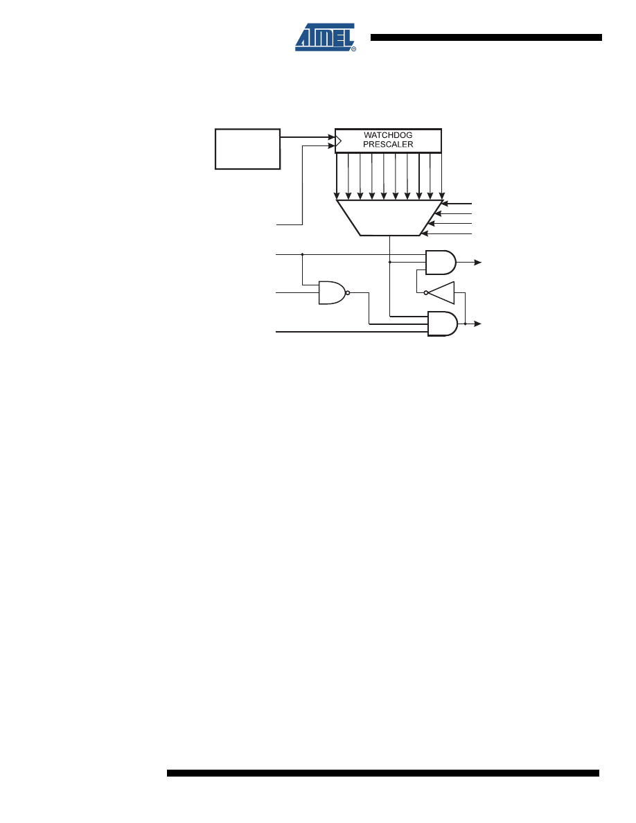
38
2535J–AVR–08/10
ATtiny13
value is reached. If the system doesn't restart the counter, an interrupt or system reset will be
issued.
Figure 8-7.
Watchdog Timer
In Interrupt mode, the WDT gives an interrupt when the timer expires. This interrupt can be used
to wake the device from sleep-modes, and also as a general system timer. One example is to
limit the maximum time allowed for certain operations, giving an interrupt when the operation
has run longer than expected. In System Reset mode, the WDT gives a reset when the timer
expires. This is typically used to prevent system hang-up in case of runaway code. The third
mode, Interrupt and System Reset mode, combines the other two modes by first giving an inter-
rupt and then switch to System Reset mode. This mode will for instance allow a safe shutdown
by saving critical parameters before a system reset.
The Watchdog always on (WDTON) fuse, if programmed, will force the Watchdog Timer to Sys-
tem Reset mode. With the fuse programmed the System Reset mode bit (WDE) and Interrupt
mode bit (WDTIE) are locked to 1 and 0 respectively. To further ensure program security, altera-
tions to the Watchdog set-up must follow timed sequences. The sequence for clearing WDE and
changing time-out configuration is as follows:
1. In the same operation, write a logic one to the Watchdog change enable bit (WDCE)
and WDE. A logic one must be written to WDE regardless of the previous value of the
WDE bit.
2. Within the next four clock cycles, write the WDE and Watchdog prescaler bits (WDP) as
desired, but with the WDCE bit cleared. This must be done in one operation.
128kHz
OSCILLATOR
OSC/2K
OSC/4K
OSC/8K
OSC/16K
OSC/32K
OSC/64K
OSC/128K
OSC/256K
OSC/512K
OSC/1024K
WDP0
WDP1
WDP2
WDP3
WATCHDOG
RESET
WDE
WDTIF
WDTIE
MCU RESET
INTERRUPT

39
2535J–AVR–08/10
ATtiny13
The following code example shows one assembly and one C function for turning off the Watch-
dog Timer. The example assumes that interrupts are controlled (e.g. by disabling interrupts
globally) so that no interrupts will occur during the execution of these functions.
Note:
1. The example code assumes that the part specific header file is included.
If the Watchdog is accidentally enabled, for example by a runaway pointer or brown-out condi-
tion, the device will be reset and the Watchdog Timer will stay enabled. If the code is not set up
to handle the Watchdog, this might lead to an eternal loop of time-out resets. To avoid this situa-
Assembly Code Example
WDT_off:
; Turn off global interrupt
cli
; Reset Watchdog Timer
wdr
; Clear WDRF in MCUSR
in
r16, MCUSR
andi
r16, (0xff - (1<<WDRF))
out
MCUSR, r16
; Write logical one to WDCE and WDE
; Keep old prescaler setting to prevent unintentional time-out
in
r16, WDTCR
ori
r16, (1<<WDCE) | (1<<WDE)
out
WDTCR, r16
; Turn off WDT
ldi
r16, (0<<WDE)
out
WDTCR, r16
; Turn on global interrupt
sei
ret
C Code Example
void WDT_off(void)
{
__disable_interrupt();
__watchdog_reset();
/* Clear WDRF in MCUSR */
MCUSR &= ~(1<<WDRF);
/* Write logical one to WDCE and WDE */
/* Keep old prescaler setting to prevent unintentional time-out
*/
WDTCR |= (1<<WDCE) | (1<<WDE);
/* Turn off WDT */
WDTCR = 0x00;
__enable_interrupt();
}

40
2535J–AVR–08/10
ATtiny13
tion, the application software should always clear the Watchdog System Reset Flag (WDRF)
and the WDE control bit in the initialisation routine, even if the Watchdog is not in use.
The following code example shows one assembly and one C function for changing the time-out
value of the Watchdog Timer.
Note:
1. The example code assumes that the part specific header file is included.
The Watchdog Timer should be reset before any change of the WDP bits, since a change in the
WDP bits can result in a time-out when switching to a shorter time-out period.
Assembly Code Example
WDT_Prescaler_Change:
; Turn off global interrupt
cli
; Reset Watchdog Timer
wdr
; Start timed sequence
in
r16, WDTCR
ori
r16, (1<<WDCE) | (1<<WDE)
out
WDTCR, r16
; -- Got four cycles to set the new values from here -
; Set new prescaler(time-out) value = 64K cycles (~0.5 s)
ldi
r16, (1<<WDE) | (1<<WDP2) | (1<<WDP0)
out
WDTCR, r16
; -- Finished setting new values, used 2 cycles -
; Turn on global interrupt
sei
ret
C Code Example
void WDT_Prescaler_Change(void)
{
__disable_interrupt();
__watchdog_reset();
/* Start timed sequence */
WDTCR |= (1<<WDCE) | (1<<WDE);
/* Set new prescaler(time-out) value = 64K cycles (~0.5 s) */
WDTCR = (1<<WDE) | (1<<WDP2) | (1<<WDP0);
__enable_interrupt();
}

41
2535J–AVR–08/10
ATtiny13
8.4
Register Description
8.4.1
MCUSR – MCU Status Register
The MCU Status Register provides information on which reset source caused an MCU Reset.
• Bits 7:4 – Res: Reserved Bits
These bits are reserved bits in the ATtiny13 and will always read as zero.
• Bit 3 – WDRF: Watchdog Reset Flag
This bit is set if a Watchdog Reset occurs. The bit is reset by a Power-on Reset, or by writing a
logic zero to the flag.
• Bit 2 – BORF: Brown-out Reset Flag
This bit is set if a Brown-out Reset occurs. The bit is reset by a Power-on Reset, or by writing a
logic zero to the flag.
• Bit 1 – EXTRF: External Reset Flag
This bit is set if an External Reset occurs. The bit is reset by a Power-on Reset, or by writing a
logic zero to the flag.
• Bit 0 – PORF: Power-on Reset Flag
This bit is set if a Power-on Reset occurs. The bit is reset only by writing a logic zero to the flag.
To make use of the Reset Flags to identify a reset condition, the user should read and then reset
the MCUSR as early as possible in the program. If the register is cleared before another reset
occurs, the source of the reset can be found by examining the Reset Flags.
8.4.2
WDTCR – Watchdog Timer Control Register
• Bit 7 - WDTIF: Watchdog Timer Interrupt Flag
This bit is set when a time-out occurs in the Watchdog Timer and the Watchdog Timer is config-
ured for interrupt. WDTIF is cleared by hardware when executing the corresponding interrupt
handling vector. Alternatively, WDTIF is cleared by writing a logic one to the flag. When the I-bit
in SREG and WDTIE are set, the Watchdog Time-out Interrupt is executed.
• Bit 6 - WDTIE: Watchdog Timer Interrupt Enable
When this bit is written to one and the I-bit in the Status Register is set, the Watchdog Interrupt is
enabled. If WDE is cleared in combination with this setting, the Watchdog Timer is in Interrupt
Mode, and the corresponding interrupt is executed if time-out in the Watchdog Timer occurs.
If WDE is set, the Watchdog Timer is in Interrupt and System Reset Mode. The first time-out in
the Watchdog Timer will set WDTIF. Executing the corresponding interrupt vector will clear
WDTIE and WDTIF automatically by hardware (the Watchdog goes to System Reset Mode).
Bit
7
6
5
4
3
2
1
0
–
–
–
–
WDRF
BORF
EXTRF
PORF
MCUSR
Read/Write
R
R
R
R
R/W
R/W
R/W
R/W
Initial Value
0
0
0
0
See Bit Description
Bit
7
6
5
4
3
2
1
0
WDTIF
WDTIE
WDP3
WDCE
WDE
WDP2
WDP1
WDP0
WDTCR
Read/Write
R/W
R/W
R/W
R/W
R/W
R/W
R/W
R/W
Initial Value
0
0
0
0
X
0
0
0
42
2535J–AVR–08/10
ATtiny13
This is useful for keeping the Watchdog Timer security while using the interrupt. To stay in Inter-
rupt and System Reset Mode, WDTIE must be set after each interrupt. This should however not
be done within the interrupt service routine itself, as this might compromise the safety-function of
the Watchdog System Reset mode. If the interrupt is not executed before the next time-out, a
System Reset will be applied.
Note:
1. WDTON fuse set to “0“ means programmed and “1“ means unprogrammed.
• Bit 4 - WDCE: Watchdog Change Enable
This bit is used in timed sequences for changing WDE and prescaler bits. To clear the WDE bit,
and/or change the prescaler bits, WDCE must be set.
Once written to one, hardware will clear WDCE after four clock cycles.
• Bit 3 - WDE: Watchdog System Reset Enable
WDE is overridden by WDRF in MCUSR. This means that WDE is always set when WDRF is
set. To clear WDE, WDRF must be cleared first. This feature ensures multiple resets during con-
ditions causing failure, and a safe start-up after the failure.
• Bit 5, 2:0 - WDP[3:0]: Watchdog Timer Prescaler 3, 2, 1 and 0
The WDP[3:0] bits determine the Watchdog Timer prescaling when the Watchdog Timer is run-
ning. The different prescaling values and their corresponding time-out periods are shown in
..
Table 8-1.
Watchdog Timer Configuration
WDTON
WDE
WDTIE
Mode
Action on Time-out
1
0
0
Stopped
None
1
0
1
Interrupt Mode
Interrupt
1
1
0
System Reset Mode
Reset
1
1
1
Interrupt and System Reset
Mode
Interrupt, then go to System
Reset Mode
0
x
x
System Reset Mode
Reset
Table 8-2.
Watchdog Timer Prescale Select
WDP3
WDP2
WDP1
WDP0
Number of WDT Oscillator
Cycles
Typical Time-out at
V
CC
= 5.0V
0
0
0
0
2K (2048) cycles
16 ms
0
0
0
1
4K (4096) cycles
32 ms
0
0
1
0
8K (8192) cycles
64 ms
0
0
1
1
16K (16384) cycles
0.125 s
0
1
0
0
32K (32768) cycles
0.25 s
0
1
0
1
64K (65536) cycles
0.5 s
0
1
1
0
128K (131072) cycles
1.0 s
0
1
1
1
256K (262144) cycles
2.0 s
1
0
0
0
512K (524288) cycles
4.0 s
1
0
0
1
1024K (1048576) cycles
8.0 s
43
2535J–AVR–08/10
ATtiny13
1
0
1
0
Reserved
1
0
1
1
1
1
0
0
1
1
0
1
1
1
1
0
1
1
1
1
Table 8-2.
Watchdog Timer Prescale Select
WDP3
WDP2
WDP1
WDP0
Number of WDT Oscillator
Cycles
Typical Time-out at
V
CC
= 5.0V

44
2535J–AVR–08/10
ATtiny13
9. Interrupts
This section describes the specifics of the interrupt handling as performed in ATtiny13. For a
general explanation of the AVR interrupt handling, refer to
“Reset and Interrupt Handling” on
9.1
Interrupt Vectors
The interrupt vectors of ATtiny13 are described in
below.
If the program never enables an interrupt source, the Interrupt Vectors are not used, and regular
program code can be placed at these locations.
The most typical and general program setup for the Reset and Interrupt Vector Addresses in
ATtiny13 is:
Address
Labels Code
Comments
0x0000
rjmp
RESET
; Reset Handler
0x0001
rjmp
EXT_INT0
; IRQ0 Handler
0x0002
rjmp
PCINT0
; PCINT0 Handler
0x0003
rjmp
TIM0_OVF
; Timer0 Overflow Handler
0x0004
rjmp
EE_RDY
; EEPROM Ready Handler
0x0005
rjmp
ANA_COMP
; Analog Comparator Handler
0x0006
rjmp
TIM0_COMPA
; Timer0 CompareA Handler
0x0007
rjmp
TIM0_COMPB
; Timer0 CompareB Handler
0x0008
rjmp
WATCHDOG
; Watchdog Interrupt Handler
0x0009
rjmp
ADC
; ADC Conversion Handler
;
0x000A
RESET: ldi
r16, low(RAMEND); Main program start
0x000B
out
SPL,r16
; Set Stack Pointer to top of RAM
0x000C
sei
; Enable interrupts
0x000D
<instr> xxx
...
... ... ...
Table 9-1.
Reset and Interrupt Vectors
Vector No.
Program Address
Source
Interrupt Definition
1
0x0000
RESET
External Pin, Power-on Reset,
Brown-out Reset, Watchdog Reset
2
0x0001
INT0
External Interrupt Request 0
3
0x0002
PCINT0
Pin Change Interrupt Request 0
4
0x0003
TIM0_OVF
Timer/Counter Overflow
5
0x0004
EE_RDY
EEPROM Ready
6
0x0005
ANA_COMP
Analog Comparator
7
0x0006
TIM0_COMPA
Timer/Counter Compare Match A
8
0x0007
TIM0_COMPB
Timer/Counter Compare Match B
9
0x0008
WDT
Watchdog Time-out
10
0x0009
ADC
ADC Conversion Complete
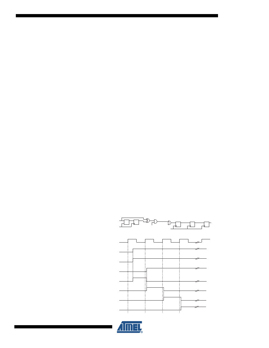
45
2535J–AVR–08/10
ATtiny13
9.2
External Interrupts
The External Interrupts are triggered by the INT0 pin or any of the PCINT5..0 pins. Observe that,
if enabled, the interrupts will trigger even if the INT0 or PCINT5..0 pins are configured as out-
puts. This feature provides a way of generating a software interrupt. Pin change interrupts PCI
will trigger if any enabled PCINT5..0 pin toggles. The PCMSK Register control which pins con-
tribute to the pin change interrupts. Pin change interrupts on PCINT5..0 are detected
asynchronously. This implies that these interrupts can be used for waking the part also from
sleep modes other than Idle mode.
The INT0 interrupts can be triggered by a falling or rising edge or a low level. This is set up as
indicated in the specification for the MCU Control Register – MCUCR. When the INT0 interrupt is
enabled and is configured as level triggered, the interrupt will trigger as long as the pin is held
low. Note that recognition of falling or rising edge interrupts on INT0 requires the presence of an
I/O clock, described in
“Clock Systems and their Distribution” on page 23
.
9.2.1
Low Level Interrupt
A low level interrupt on INT0 is detected asynchronously. This implies that this interrupt can be
used for waking the part also from sleep modes other than Idle mode. The I/O clock is halted in
all sleep modes except Idle mode.
Note that if a level triggered interrupt is used for wake-up from Power-down, the required level
must be held long enough for the MCU to complete the wake-up to trigger the level interrupt. If
the level disappears before the end of the Start-up Time, the MCU will still wake up, but no inter-
rupt will be generated. The start-up time is defined by the SUT and CKSEL fuses as described in
“System Clock and Clock Options” on page 23
If the low level on the interrupt pin is removed before the device has woken up then program
execution will not be diverted to the interrupt service routine but continue from the instruction fol-
lowing the SLEEP command.
9.2.2
Pin Change Interrupt Timing
An example of timing of a pin change interrupt is shown in
below.
Figure 9-1.
Timing of pin change interrupts
clk
PCINT(n)
pin_lat
pin_sync
pcint_in_(n)
pcint_syn
pcint_setflag
PCIF
PCINT(0)
pin_sync
pcint_syn
pin_lat
D Q
LE
pcint_setflag
PCIF
clk
clk
PCINT(0) in PCMSK(x)
pcint_in_(0)
0
x
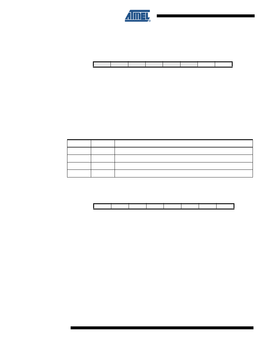
46
2535J–AVR–08/10
ATtiny13
9.3
Register Description
9.3.1
MCUCR – MCU Control Register
The External Interrupt Control Register A contains control bits for interrupt sense control.
• Bits 1, 0 – ISC01, ISC00: Interrupt Sense Control 0 Bit 1 and Bit 0
The External Interrupt 0 is activated by the external pin INT0 if the SREG I-flag and the corre-
sponding interrupt mask are set. The level and edges on the external INT0 pin that activate the
interrupt are defined in
. The value on the INT0 pin is sampled before
detecting edges. If edge or toggle interrupt is selected, pulses that last longer than one clock
period will generate an interrupt. Shorter pulses are not guaranteed to generate an interrupt. If
low level interrupt is selected, the low level must be held until the completion of the currently
executing instruction to generate an interrupt.
9.3.2
GIMSK – General Interrupt Mask Register
• Bits 7, 4:0 – Res: Reserved Bits
These bits are reserved bits in the ATtiny13 and will always read as zero.
• Bit 6 – INT0: External Interrupt Request 0 Enable
When the INT0 bit is set (one) and the I-bit in the Status Register (SREG) is set (one), the exter-
nal pin interrupt is enabled. The Interrupt Sense Control0 bits 1/0 (ISC01 and ISC00) in the MCU
Control Register (MCUCR) define whether the external interrupt is activated on rising and/or fall-
ing edge of the INT0 pin or level sensed. Activity on the pin will cause an interrupt request even
if INT0 is configured as an output. The corresponding interrupt of External Interrupt Request 0 is
executed from the INT0 Interrupt Vector.
• Bit 5 – PCIE: Pin Change Interrupt Enable
When the PCIE bit is set (one) and the I-bit in the Status Register (SREG) is set (one), pin
change interrupt is enabled. Any change on any enabled PCINT5..0 pin will cause an interrupt.
The corresponding interrupt of Pin Change Interrupt Request is executed from the PCI Interrupt
Vector. PCINT5..0 pins are enabled individually by the PCMSK Register.
Bit
7
6
5
4
3
2
1
0
–
PUD
SE
SM1
SM0
–
ISC01
ISC00
MCUCR
Read/Write
R
R/W
R/W
R/W
R/W
R
R/W
R/W
Initial Value
0
0
0
0
0
0
0
0
Table 9-2.
Interrupt 0 Sense Control
ISC01
ISC00
Description
0
0
The low level of INT0 generates an interrupt request.
0
1
Any logical change on INT0 generates an interrupt request.
1
0
The falling edge of INT0 generates an interrupt request.
1
1
The rising edge of INT0 generates an interrupt request.
Bit
7
6
5
4
3
2
1
0
–
INT0
PCIE
–
–
–
–
–
GIMSK
Read/Write
R
R/W
R/W
R
R
R
R
R
Initial Value
0
0
0
0
0
0
0
0

47
2535J–AVR–08/10
ATtiny13
9.3.3
GIFR – General Interrupt Flag Register
• Bits 7, 4:0 – Res: Reserved Bits
These bits are reserved bits in the ATtiny13 and will always read as zero.
• Bit 6 – INTF0: External Interrupt Flag 0
When an edge or logic change on the INT0 pin triggers an interrupt request, INTF0 becomes set
(one). If the I-bit in SREG and the INT0 bit in GIMSK are set (one), the MCU will jump to the cor-
responding Interrupt Vector. The flag is cleared when the interrupt routine is executed.
Alternatively, the flag can be cleared by writing a logical one to it. This flag is always cleared
when INT0 is configured as a level interrupt.
• Bit 5 – PCIF: Pin Change Interrupt Flag
When a logic change on any PCINT5:0 pin triggers an interrupt request, PCIF becomes set
(one). If the I-bit in SREG and the PCIE bit in GIMSK are set (one), the MCU will jump to the cor-
responding Interrupt Vector. The flag is cleared when the interrupt routine is executed.
Alternatively, the flag can be cleared by writing a logical one to it.
9.3.4
PCMSK – Pin Change Mask Register
• Bits 7, 6 – Res: Reserved Bits
These bits are reserved bits in the ATtiny13 and will always read as zero.
• Bits 5:0 – PCINT5:0: Pin Change Enable Mask 5:0
Each PCINT5:0 bit selects whether pin change interrupt is enabled on the corresponding I/O pin.
If PCINT5:0 is set and the PCIE bit in GIMSK is set, pin change interrupt is enabled on the cor-
responding I/O pin. If PCINT5:0 is cleared, pin change interrupt on the corresponding I/O pin is
disabled.
Bit
7
6
5
4
3
2
1
0
–
INTF0
PCIF
–
–
–
–
–
GIFR
Read/Write
R
R/W
R/W
R
R
R
R
R
Initial Value
0
0
0
0
0
0
0
0
Bit
7
6
5
4
3
2
1
0
–
–
PCINT5
PCINT4
PCINT3
PCINT2
PCINT1
PCINT0
PCMSK
Read/Write
R
R
R/W
R/W
R/W
R/W
R/W
R/W
Initial Value
0
0
0
0
0
0
0
0
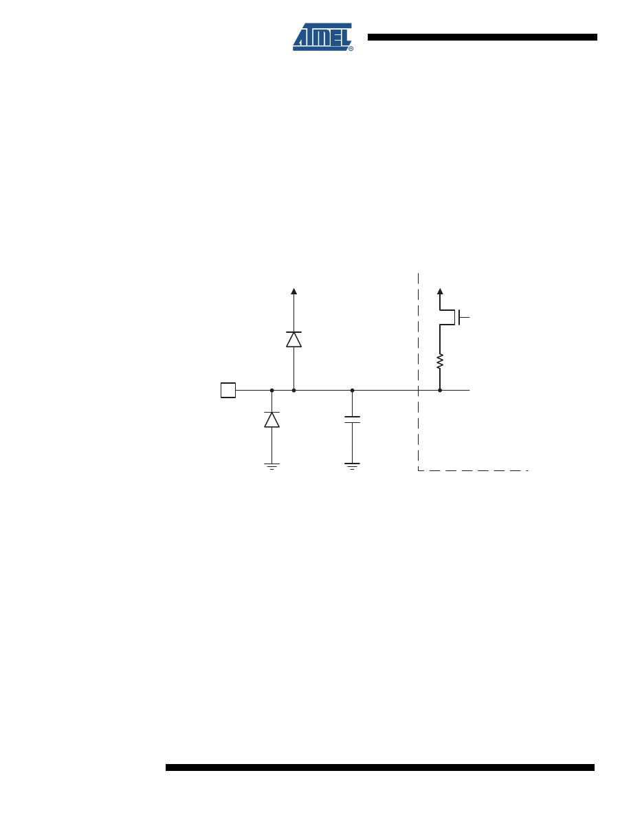
48
2535J–AVR–08/10
ATtiny13
10. I/O Ports
10.1 Overview
All AVR ports have true Read-Modify-Write functionality when used as general digital I/O ports.
This means that the direction of one port pin can be changed without unintentionally changing
the direction of any other pin with the SBI and CBI instructions. The same applies when chang-
ing drive value (if configured as output) or enabling/disabling of pull-up resistors (if configured as
input). Each output buffer has symmetrical drive characteristics with both high sink and source
capability. The pin driver is strong enough to drive LED displays directly. All port pins have indi-
vidually selectable pull-up resistors with a supply-voltage invariant resistance. All I/O pins have
protection diodes to both V
CC
and Ground as indicated in
. Refer to
for a complete list of parameters.
Figure 10-1. I/O Pin Equivalent Schematic
All registers and bit references in this section are written in general form. A lower case “x” repre-
sents the numbering letter for the port, and a lower case “n” represents the bit number. However,
when using the register or bit defines in a program, the precise form must be used. For example,
PORTB3 for bit no. 3 in Port B, here documented generally as PORTxn. The physical I/O Regis-
ters and bit locations are listed in
“Register Description” on page 56
.
Three I/O memory address locations are allocated for each port, one each for the Data Register
– PORTx, Data Direction Register – DDRx, and the Port Input Pins – PINx. The Port Input Pins
I/O location is read only, while the Data Register and the Data Direction Register are read/write.
However, writing a logic one to a bit in the PINx Register, will result in a toggle in the correspond-
ing bit in the Data Register. In addition, the Pull-up Disable – PUD bit in MCUCR disables the
pull-up function for all pins in all ports when set.
Using the I/O port as General Digital I/O is described in
“Ports as General Digital I/O” on page
. Most port pins are multiplexed with alternate functions for the peripheral features on the
device. How each alternate function interferes with the port pin is described in
. Refer to the individual module sections for a full description of the alter-
nate functions.
C
pin
Logic
R
pu
See Figure
"General Digital I/O" for
Details
Pxn
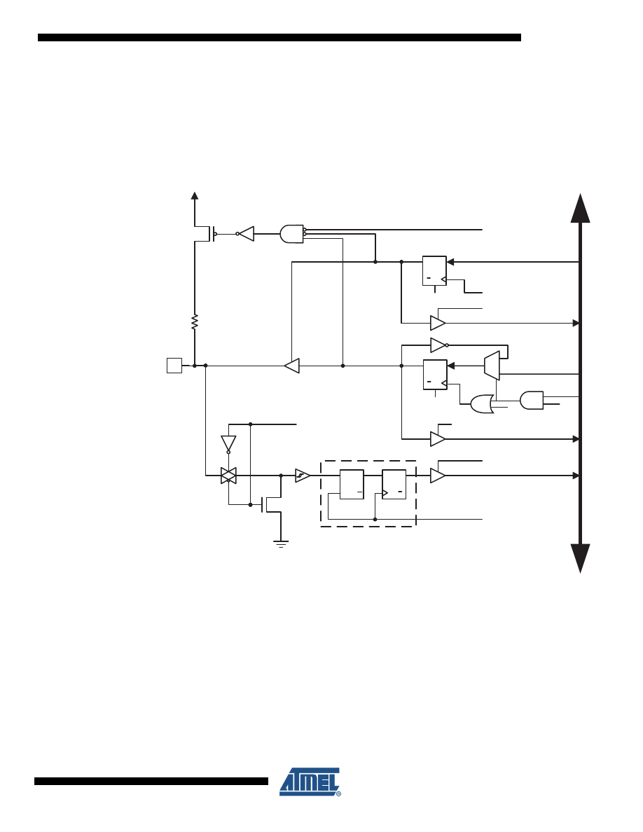
49
2535J–AVR–08/10
ATtiny13
Note that enabling the alternate function of some of the port pins does not affect the use of the
other pins in the port as general digital I/O.
10.2 Ports as General Digital I/O
The ports are bi-directional I/O ports with optional internal pull-ups.
shows a functional description of one I/O-port pin, here generically called Pxn.
Figure 10-2. General Digital I/O
Note:
1. WRx, WPx, WDx, RRx, RPx, and RDx are common to all pins within the same port. clk
I/O
,
SLEEP, and PUD are common to all ports.
10.2.1
Configuring the Pin
Each port pin consists of three register bits: DDxn, PORTxn, and PINxn. As shown in
, the DDxn bits are accessed at the DDRx I/O address, the PORTxn bits
at the PORTx I/O address, and the PINxn bits at the PINx I/O address.
The DDxn bit in the DDRx Register selects the direction of this pin. If DDxn is written logic one,
Pxn is configured as an output pin. If DDxn is written logic zero, Pxn is configured as an input
pin.
clk
RPx
RRx
RDx
WDx
PUD
SYNCHRONIZER
WDx:
WRITE DDRx
WRx:
WRITE PORTx
RRx:
READ PORTx REGISTER
RPx:
READ PORTx PIN
PUD:
PULLUP DISABLE
clk
I/O
:
I/O CLOCK
RDx:
READ DDRx
D
L
Q
Q
RESET
RESET
Q
Q
D
Q
Q
D
CLR
PORTxn
Q
Q
D
CLR
DDxn
PINxn
D
ATA
B
U
S
SLEEP
SLEEP:
SLEEP CONTROL
Pxn
I/O
WPx
0
1
WRx
WPx:
WRITE PINx REGISTER

50
2535J–AVR–08/10
ATtiny13
If PORTxn is written logic one when the pin is configured as an input pin, the pull-up resistor is
activated. To switch the pull-up resistor off, PORTxn has to be written logic zero or the pin has to
be configured as an output pin. The port pins are tri-stated when reset condition becomes active,
even if no clocks are running.
If PORTxn is written logic one when the pin is configured as an output pin, the port pin is driven
high (one). If PORTxn is written logic zero when the pin is configured as an output pin, the port
pin is driven low (zero).
10.2.2
Toggling the Pin
Writing a logic one to PINxn toggles the value of PORTxn, independent on the value of DDRxn.
Note that the SBI instruction can be used to toggle one single bit in a port.
10.2.3
Switching Between Input and Output
When switching between tri-state ({DDxn, PORTxn} = 0b00) and output high ({DDxn, PORTxn}
= 0b11), an intermediate state with either pull-up enabled {DDxn, PORTxn} = 0b01) or output
low ({DDxn, PORTxn} = 0b10) must occur. Normally, the pull-up enabled state is fully accept-
able, as a high-impedant environment will not notice the difference between a strong high driver
and a pull-up. If this is not the case, the PUD bit in the MCUCR Register can be set to disable all
pull-ups in all ports.
Switching between input with pull-up and output low generates the same problem. The user
must use either the tri-state ({DDxn, PORTxn} = 0b00) or the output high state ({DDxn, PORTxn}
= 0b10) as an intermediate step.
summarizes the control signals for the pin value.
10.2.4
Reading the Pin Value
Independent of the setting of Data Direction bit DDxn, the port pin can be read through the
PINxn Register bit. As shown in
, the PINxn Register bit and the preced-
ing latch constitute a synchronizer. This is needed to avoid metastability if the physical pin
changes value near the edge of the internal clock, but it also introduces a delay.
shows a timing diagram of the synchronization when reading an externally applied pin
value. The maximum and minimum propagation delays are denoted t
pd,max
and t
pd,min
respectively.
Table 10-1.
Port Pin Configurations
DDxn
PORTxn
PUD
(in MCUCR)
I/O
Pull-up
Comment
0
0
X
Input
No
Tri-state (Hi-Z)
0
1
0
Input
Yes
Pxn will source current if ext. pulled low.
0
1
1
Input
No
Tri-state (Hi-Z)
1
0
X
Output
No
Output Low (Sink)
1
1
X
Output
No
Output High (Source)
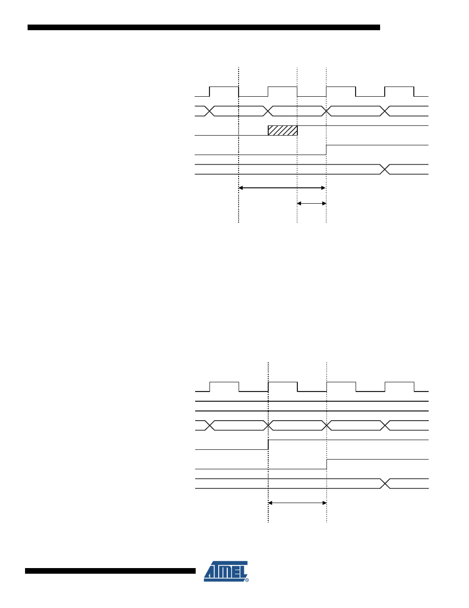
51
2535J–AVR–08/10
ATtiny13
Figure 10-3. Synchronization when Reading an Externally Applied Pin value
Consider the clock period starting shortly after the first falling edge of the system clock. The latch
is closed when the clock is low, and goes transparent when the clock is high, as indicated by the
shaded region of the “SYNC LATCH” signal. The signal value is latched when the system clock
goes low. It is clocked into the PINxn Register at the succeeding positive clock edge. As indi-
cated by the two arrows tpd,max and tpd,min, a single signal transition on the pin will be delayed
between ½ and 1½ system clock period depending upon the time of assertion.
When reading back a software assigned pin value, a nop instruction must be inserted as indi-
cated in
. The out instruction sets the “SYNC LATCH” signal at the
positive edge of the clock. In this case, the delay tpd through the synchronizer is one system
clock period.
Figure 10-4. Synchronization when Reading a Software Assigned Pin Value
XXX
in r17, PINx
0x00
0xFF
INSTRUCTIONS
SYNC LATCH
PINxn
r17
XXX
SYSTEM CLK
t
pd, max
t
pd, min
out PORTx, r16
nop
in r17, PINx
0xFF
0x00
0xFF
SYSTEM CLK
r16
INSTRUCTIONS
SYNC LATCH
PINxn
r17
t
pd

52
2535J–AVR–08/10
ATtiny13
The following code example shows how to set port B pins 0 and 1 high, 2 and 3 low, and define
the port pins from 4 to 5 as input with a pull-up assigned to port pin 4. The resulting pin values
are read back again, but as previously discussed, a nop instruction is included to be able to read
back the value recently assigned to some of the pins.
Note:
1. For the assembly program, two temporary registers are used to minimize the time from pull-
ups are set on pins 0, 1 and 4, until the direction bits are correctly set, defining bit 2 and 3 as
low and redefining bits 0 and 1 as strong high drivers.
10.2.5
Digital Input Enable and Sleep Modes
As shown in
, the digital input signal can be clamped to ground at the
input of the schmitt-trigger. The signal denoted SLEEP in the figure, is set by the MCU Sleep
Controller in Power-down mode, Power-save mode, and Standby mode to avoid high power
consumption if some input signals are left floating, or have an analog signal level close to V
CC
/2.
SLEEP is overridden for port pins enabled as external interrupt pins. If the external interrupt
request is not enabled, SLEEP is active also for these pins. SLEEP is also overridden by various
other alternate functions as described in
“Alternate Port Functions” on page 53
If a logic high level (“one”) is present on an asynchronous external interrupt pin configured as
“Interrupt on Rising Edge, Falling Edge, or Any Logic Change on Pin” while the external interrupt
is not enabled, the corresponding External Interrupt Flag will be set when resuming from the
Assembly Code Example
...
; Define pull-ups and set outputs high
; Define directions for port pins
ldi
r16,(1<<PB4)|(1<<PB1)|(1<<PB0)
ldi
r17,(1<<DDB3)|(1<<DDB2)|(1<<DDB1)|(1<<DDB0)
out
PORTB,r16
out
DDRB,r17
; Insert nop for synchronization
nop
; Read port pins
in
r16,PINB
...
C Code Example
unsigned char
i;
...
/* Define pull-ups and set outputs high */
/* Define directions for port pins */
PORTB = (1<<PB4)|(1<<PB1)|(1<<PB0);
DDRB = (1<<DDB3)|(1<<DDB2)|(1<<DDB1)|(1<<DDB0);
/* Insert nop for synchronization*/
__no_operation();
/* Read port pins */
i = PINB;
...
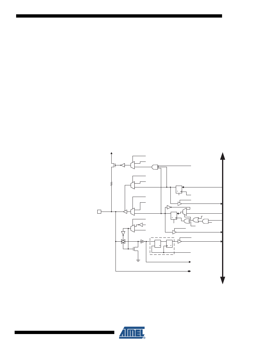
53
2535J–AVR–08/10
ATtiny13
above mentioned Sleep mode, as the clamping in these sleep mode produces the requested
logic change.
10.2.6
Unconnected Pins
If some pins are unused, it is recommended to ensure that these pins have a defined level. Even
though most of the digital inputs are disabled in the deep sleep modes as described above, float-
ing inputs should be avoided to reduce current consumption in all other modes where the digital
inputs are enabled (Reset, Active mode and Idle mode).
The simplest method to ensure a defined level of an unused pin, is to enable the internal pull-up.
In this case, the pull-up will be disabled during reset. If low power consumption during reset is
important, it is recommended to use an external pull-up or pull-down. Connecting unused pins
directly to V
CC
or GND is not recommended, since this may cause excessive currents if the pin is
accidentally configured as an output.
10.3 Alternate Port Functions
Most port pins have alternate functions in addition to being general digital I/Os.
shows how port pin control signals from the simplified
by alternate functions.
Figure 10-5. Alternate Port Functions
Note:
WRx, WPx, WDx, RRx, RPx, and RDx are common to all pins within the same port. clk
I/O
, SLEEP,
and PUD are common to all ports. All other signals are unique for each pin.
clk
RPx
RRx
WRx
RDx
WDx
PUD
SYNCHRONIZER
WDx:
WRITE DDRx
WRx:
WRITE PORTx
RRx:
READ PORTx REGISTER
RPx:
READ PORTx PIN
PUD:
PULLUP DISABLE
clk
I/O
:
I/O CLOCK
RDx:
READ DDRx
D
L
Q
Q
SET
CLR
0
1
0
1
0
1
DIxn
AIOxn
DIEOExn
PVOVxn
PVOExn
DDOVxn
DDOExn
PUOExn
PUOVxn
PUOExn:
Pxn PULL-UP OVERRIDE ENABLE
PUOVxn:
Pxn PULL-UP OVERRIDE VALUE
DDOExn:
Pxn DATA DIRECTION OVERRIDE ENABLE
DDOVxn:
Pxn DATA DIRECTION OVERRIDE VALUE
PVOExn:
Pxn PORT VALUE OVERRIDE ENABLE
PVOVxn:
Pxn PORT VALUE OVERRIDE VALUE
DIxn:
DIGITAL INPUT PIN n ON PORTx
AIOxn:
ANALOG INPUT/OUTPUT PIN n ON PORTx
RESET
RESET
Q
Q
D
CLR
Q
Q
D
CLR
Q
Q
D
CLR
PINxn
PORTxn
DDxn
D
ATA
B
U
S
0
1
DIEOVxn
SLEEP
DIEOExn: Pxn DIGITAL INPUT-ENABLE OVERRIDE ENABLE
DIEOVxn: Pxn DIGITAL INPUT-ENABLE OVERRIDE VALUE
SLEEP:
SLEEP CONTROL
Pxn
I/O
0
1
PTOExn
PTOExn:
Pxn, PORT TOGGLE OVERRIDE ENABLE
WPx:
WRITE PINx
WPx

54
2535J–AVR–08/10
ATtiny13
The overriding signals may not be present in all port pins, but
serves as a generic
description applicable to all port pins in the AVR microcontroller family.
summarizes the function of the overriding signals. The pin and port
are not shown in the succeeding tables. The overriding
signals are generated internally in the modules having the alternate function.
The following subsections shortly describe the alternate functions for each port, and relate the
overriding signals to the alternate function. Refer to the alternate function description for further
details.
10.3.1
Alternate Functions of Port B
The Port B pins with alternate function are shown in
.
Table 10-2.
Generic Description of Overriding Signals for Alternate Functions
Signal Name
Full Name
Description
PUOE
Pull-up
Override Enable
If this signal is set, the pull-up enable is controlled by the
PUOV signal. If this signal is cleared, the pull-up is enabled
when {DDxn, PORTxn, PUD} = 0b010.
PUOV
Pull-up
Override Value
If PUOE is set, the pull-up is enabled/disabled when PUOV
is set/cleared, regardless of the setting of the DDxn,
PORTxn, and PUD Register bits.
DDOE
Data Direction
Override Enable
If this signal is set, the Output Driver Enable is controlled by
the DDOV signal. If this signal is cleared, the Output driver
is enabled by the DDxn Register bit.
DDOV
Data Direction
Override Value
If DDOE is set, the Output Driver is enabled/disabled when
DDOV is set/cleared, regardless of the setting of the DDxn
Register bit.
PVOE
Port Value
Override Enable
If this signal is set and the Output Driver is enabled, the port
value is controlled by the PVOV signal. If PVOE is cleared,
and the Output Driver is enabled, the port Value is
controlled by the PORTxn Register bit.
PVOV
Port Value
Override Value
If PVOE is set, the port value is set to PVOV, regardless of
the setting of the PORTxn Register bit.
PTOE
Port Toggle
Override Enable
If PTOE is set, the PORTxn Register bit is inverted.
DIEOE
Digital Input Enable
Override Enable
If this bit is set, the Digital Input Enable is controlled by the
DIEOV signal. If this signal is cleared, the Digital Input
Enable is determined by MCU state (Normal mode, sleep
mode).
DIEOV
Digital Input Enable
Override Value
If DIEOE is set, the Digital Input is enabled/disabled when
DIEOV is set/cleared, regardless of the MCU state (Normal
mode, sleep mode).
DI
Digital Input
This is the Digital Input to alternate functions. In the figure,
the signal is connected to the output of the schmitt-trigger
but before the synchronizer. Unless the Digital Input is used
as a clock source, the module with the alternate function
will use its own synchronizer.
AIO
Analog Input/Output
This is the Analog Input/Output to/from alternate functions.
The signal is connected directly to the pad, and can be
used bi-directionally.

55
2535J–AVR–08/10
ATtiny13
and
relate the alternate functions of Port B to the overriding signals
shown in
Note:
1. 1 when the fuse is “0” (Programmed).
Table 10-3.
Port B Pins Alternate Functions
Port Pin
Alternate Function
PB5
RESET: Reset Pin
dW:
debugWIRE I/O
ADC0: ADC Input Channel 0
PCINT5: Pin Change Interrupt, Source 5
PB4
ADC2: ADC Input Channel 2
PCINT4: Pin Change Interrupt 0, Source 4
PB3
CLKI:
External Clock Input
ADC3: ADC Input Channel 3
PCINT3: Pin Change Interrupt 0, Source 3
PB2
SCK:
Serial Clock Input
ADC1: ADC Input Channel 1
T0:
Timer/Counter0 Clock Source.
PCINT2: Pin Change Interrupt 0, Source 2
PB1
MISO:
SPI Master Data Input / Slave Data Output
AIN1:
Analog Comparator, Negative Input
OC0B: Timer/Counter0 Compare Match B Output
INT0:
External Interrupt 0 Input
PCINT1:Pin Change Interrupt 0, Source 1
PB0
MOSI:: SPI Master Data Output / Slave Data Input
AIN0:
Analog Comparator, Positive Input
OC0A: Timer/Counter0 Compare Match A output
PCINT0: Pin Change Interrupt 0, Source 0
Table 10-4.
Overriding Signals for Alternate Functions in PB5:PB3
Signal
PB5/RESET/ADC0/PCINT5
PB4/ADC2/PCINT4
PB3/ADC3/CLKI/PCINT3
PUOE
0
0
PUOV
1
0
0
DDOE
0
0
DDOV
debugWire Transmit
0
0
PVOE
0
0
0
PVOV
0
0
0
PTOE
0
0
0
DIEOE
+ (PCINT5 •
PCIE + ADC0D)
PCINT4 • PCIE + ADC2D
PCINT3 • PCIE + ADC3D
DIEOV
ADC0D
ADC2D
ADC3D
DI
PCINT5 Input
PCINT4 Input
PCINT3 Input
AIO
RESET Input, ADC0 Input
ADC2 Input
ADC3 Input
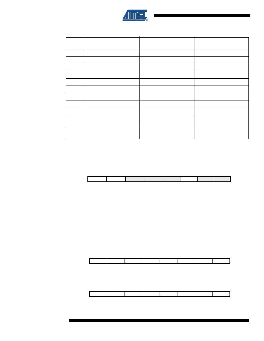
56
2535J–AVR–08/10
ATtiny13
10.4 Register Description
10.4.1
MCUCR – MCU Control Register
• Bits 7, 2– Res: Reserved Bits
These bits are reserved bits in the ATtiny13 and will always read as zero.
• Bit 6 – PUD: Pull-up Disable
When this bit is written to one, the pull-ups in the I/O ports are disabled even if the DDxn and
PORTxn Registers are configured to enable the pull-ups ({DDxn, PORTxn} = 0b01). See
for more details about this feature.
10.4.2
PORTB – Port B Data Register
10.4.3
DDRB – Port B Data Direction Register
Table 10-5.
Overriding Signals for Alternate Functions in PB2:PB0
Signal
Name
PB2/SCK/ADC1/
T0/PCINT2
PB1/MISO/AIN1/
OC0B/INT0/PCINT1
PB0/MOSI/AIN0/
AREF/OC0A/PCINT0
PUOE
0
0
0
PUOV
0
0
0
DDOE
0
0
0
DDOV
0
0
0
PVOE
0
OC0B Enable
OC0A Enable
PVOV
0
OC0B
OC0A
PTOE
0
0
0
DIEOE
PCINT2 • PCIE + ADC1D
PCINT1 • PCIE + AIN1D
PCINT0 • PCIE + AIN0D
DIEOV
ADC1D
AIN1D
AIN0D
DI
T0/INT0/
PCINT2 Input
PCINT1 Input
PCINT0 Input
AIO
ADC1 Input
Analog Comparator
Negative Input
Analog Comparator Positive
Input
Bit
7
6
5
4
3
2
1
0
–
PUD
SE
SM1
SM0
–
ISC01
ISC00
MCUCR
Read/Write
R
R/W
R/W
R/W
R/W
R
R/W
R/W
Initial Value
0
0
0
0
0
0
0
0
Bit
7
6
5
4
3
2
1
0
–
–
PORTB5
PORTB4
PORTB3
PORTB2
PORTB1
PORTB0
PORTB
Read/Write
R
R
R/W
R/W
R/W
R/W
R/W
R/W
Initial Value
0
0
0
0
0
0
0
0
Bit
7
6
5
4
3
2
1
0
–
–
DDB5
DDB4
DDB3
DDB2
DDB1
DDB0
DDRB
Read/Write
R
R
R/W
R/W
R/W
R/W
R/W
R/W
Initial Value
0
0
0
0
0
0
0
0

57
2535J–AVR–08/10
ATtiny13
10.4.4
PINB – Port B Input Pins Address
Bit
7
6
5
4
3
2
1
0
–
–
PINB5
PINB4
PINB3
PINB2
PINB1
PINB0
PINB
Read/Write
R
R
R/W
R/W
R/W
R/W
R/W
R/W
Initial Value
0
0
N/A
N/A
N/A
N/A
N/A
N/A
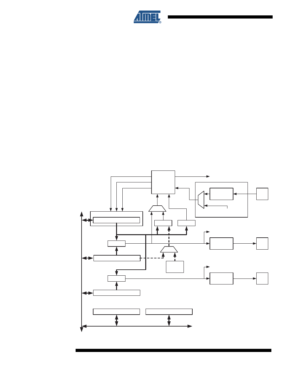
58
2535J–AVR–08/10
ATtiny13
11. 8-bit Timer/Counter0 with PWM
11.1 Features
•
Two Independent Output Compare Units
•
Double Buffered Output Compare Registers
•
Clear Timer on Compare Match (Auto Reload)
•
Glitch Free, Phase Correct Pulse Width Modulator (PWM)
•
Variable PWM Period
•
Frequency Generator
•
Three Independent Interrupt Sources (TOV0, OCF0A, and OCF0B)
11.2 Overview
Timer/Counter0 is a general purpose 8-bit Timer/Counter module, with two independent Output
Compare Units, and with PWM support. It allows accurate program execution timing (event man-
agement) and wave generation.
A simplified block diagram of the 8-bit Timer/Counter is shown in
. For
the actual placement of I/O pins, refer to
“Pinout ATtiny13/ATtiny13V” on page 2
. CPU accessi-
ble I/O Registers, including I/O bits and I/O pins, are shown in bold. The device-specific I/O
Register and bit locations are listed in the
“Register Description” on page 69
Figure 11-1. 8-bit Timer/Counter Block Diagram
Clock Select
Timer/Counter
D
ATA
B
U
S
OCRnA
OCRnB
=
=
TCNTn
Waveform
Generation
Waveform
Generation
OCnA
OCnB
=
Fixed
TOP
Value
Control Logic
=
0
TOP
BOTTOM
Count
Clear
Direction
TOVn
(Int.Req.)
OCnA
(Int.Req.)
OCnB
(Int.Req.)
TCCRnA
TCCRnB
Tn
Edge
Detector
( From Prescaler )
clk
Tn

59
2535J–AVR–08/10
ATtiny13
11.2.1
Registers
The Timer/Counter (TCNT0) and Output Compare Registers (OCR0A and OCR0B) are 8-bit
registers. Interrupt request (abbreviated to Int.Req. in the figure) signals are all visible in the
Timer Interrupt Flag Register (TIFR0). All interrupts are individually masked with the Timer Inter-
rupt Mask Register (TIMSK0). TIFR0 and TIMSK0 are not shown in the figure.
The Timer/Counter can be clocked internally, via the prescaler, or by an external clock source on
the T0 pin. The Clock Select logic block controls which clock source and edge the Timer/Counter
uses to increment (or decrement) its value. The Timer/Counter is inactive when no clock source
is selected. The output from the Clock Select logic is referred to as the timer clock (clk
T0
).
The double buffered Output Compare Registers (OCR0A and OCR0B) is compared with the
Timer/Counter value at all times. The result of the compare can be used by the Waveform Gen-
erator to generate a PWM or variable frequency output on the Output Compare pins (OC0A and
OC0B).
See “Output Compare Unit” on page 60.
for details. The Compare Match event will also
set the Compare Flag (OCF0A or OCF0B) which can be used to generate an Output Compare
interrupt request.
11.2.2
Definitions
Many register and bit references in this section are written in general form. A lower case “n”
replaces the Timer/Counter number, in this case 0. A lower case “x” replaces the Output Com-
pare Unit, in this case Compare Unit A or Compare Unit B. However, when using the register or
bit defines in a program, the precise form must be used, i.e., TCNT0 for accessing
Timer/Counter0 counter value and so on.
The definitions in
are also used extensively throughout the document.
11.3 Timer/Counter Clock Sources
The Timer/Counter can be clocked by an internal or an external clock source. The clock source
is selected by the Clock Select logic which is controlled by the Clock Select (CS02:0) bits
located in the Timer/Counter Control Register (TCCR0B). For details on clock sources and pres-
caler, see
“Timer/Counter Prescaler” on page 76
.
11.4 Counter Unit
The main part of the 8-bit Timer/Counter is the programmable bi-directional counter unit.
shows a block diagram of the counter and its surroundings.
Table 11-1.
Definitions
BOTTOM
The counter reaches the BOTTOM when it becomes 0x00.
MAX
The counter reaches its MAXimum when it becomes 0xFF (decimal 255).
TOP
The counter reaches the TOP when it becomes equal to the highest value in the
count sequence. The TOP value can be assigned to be the fixed value 0xFF
(MAX) or the value stored in the OCR0A Register. The assignment is depen-
dent on the mode of operation.
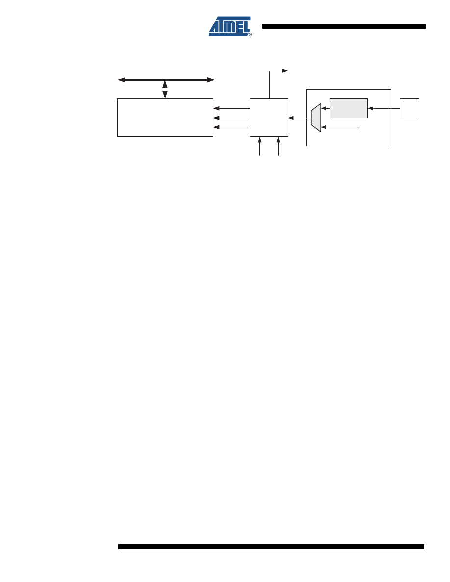
60
2535J–AVR–08/10
ATtiny13
Figure 11-2. Counter Unit Block Diagram
Signal description (internal signals):
count
Increment or decrement TCNT0 by 1.
direction
Select between increment and decrement.
clear
Clear TCNT0 (set all bits to zero).
clk
Tn
Timer/Counter clock, referred to as clk
T0
in the following.
top
Signalize that TCNT0 has reached maximum value.
bottom
Signalize that TCNT0 has reached minimum value (zero).
Depending of the mode of operation used, the counter is cleared, incremented, or decremented
at each timer clock (clk
T0
). clk
T0
can be generated from an external or internal clock source,
selected by the Clock Select bits (CS02:0). When no clock source is selected (CS02:0 = 0) the
timer is stopped. However, the TCNT0 value can be accessed by the CPU, regardless of
whether clk
T0
is present or not. A CPU write overrides (has priority over) all counter clear or
count operations.
The counting sequence is determined by the setting of the WGM01 and WGM00 bits located in
the Timer/Counter Control Register (TCCR0A) and the WGM02 bit located in the Timer/Counter
Control Register B (TCCR0B). There are close connections between how the counter behaves
(counts) and how waveforms are generated on the Output Compare output OC0A. For more
details about advanced counting sequences and waveform generation, see
The Timer/Counter Overflow Flag (TOV0) is set according to the mode of operation selected by
the WGM01:0 bits. TOV0 can be used for generating a CPU interrupt.
11.5 Output Compare Unit
The 8-bit comparator continuously compares TCNT0 with the Output Compare Registers
(OCR0A and OCR0B). Whenever TCNT0 equals OCR0A or OCR0B, the comparator signals a
match. A match will set the Output Compare Flag (OCF0A or OCF0B) at the next timer clock
cycle. If the corresponding interrupt is enabled, the Output Compare Flag generates an Output
Compare interrupt. The Output Compare Flag is automatically cleared when the interrupt is exe-
cuted. Alternatively, the flag can be cleared by software by writing a logical one to its I/O bit
location. The Waveform Generator uses the match signal to generate an output according to
operating mode set by the WGM02:0 bits and Compare Output mode (COM0x1:0) bits. The max
and bottom signals are used by the Waveform Generator for handling the special cases of the
extreme values in some modes of operation (
See “Modes of Operation” on page 63.
).
shows a block diagram of the Output Compare unit.
DATA BUS
TCNTn
Control Logic
count
TOVn
(Int.Req.)
Clock Select
top
Tn
Edge
Detector
( From Prescaler )
clk
Tn
bottom
direction
clear
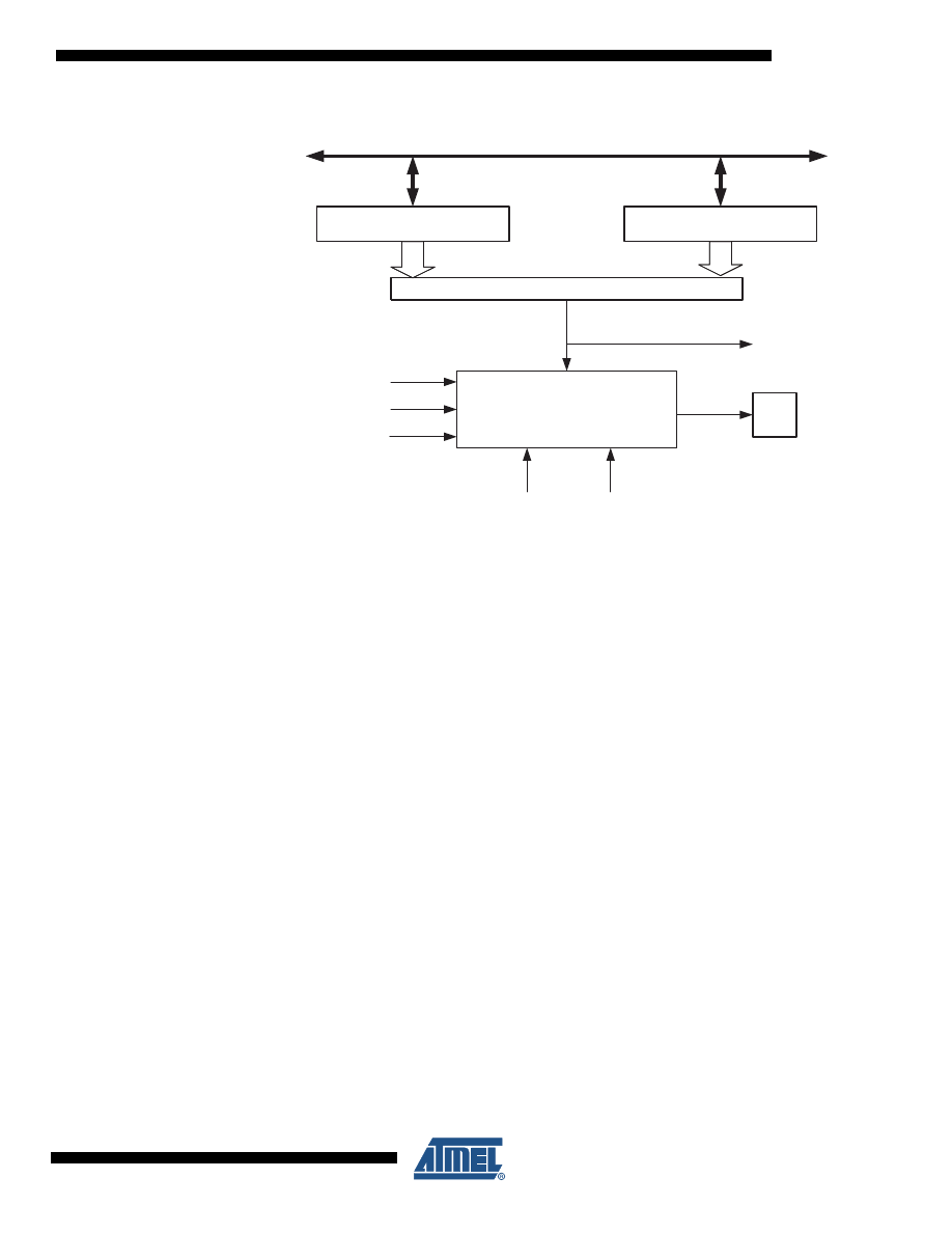
61
2535J–AVR–08/10
ATtiny13
Figure 11-3. Output Compare Unit, Block Diagram
The OCR0x Registers are double buffered when using any of the Pulse Width Modulation
(PWM) modes. For the normal and Clear Timer on Compare (CTC) modes of operation, the dou-
ble buffering is disabled. The double buffering synchronizes the update of the OCR0x Compare
Registers to either top or bottom of the counting sequence. The synchronization prevents the
occurrence of odd-length, non-symmetrical PWM pulses, thereby making the output glitch-free.
The OCR0x Register access may seem complex, but this is not case. When the double buffering
is enabled, the CPU has access to the OCR0x Buffer Register, and if double buffering is dis-
abled the CPU will access the OCR0x directly.
11.5.1
Force Output Compare
In non-PWM waveform generation modes, the match output of the comparator can be forced by
writing a one to the Force Output Compare (FOC0x) bit. Forcing Compare Match will not set the
OCF0x Flag or reload/clear the timer, but the OC0x pin will be updated as if a real Compare
Match had occurred (the COM0x1:0 bits settings define whether the OC0x pin is set, cleared or
toggled).
11.5.2
Compare Match Blocking by TCNT0 Write
All CPU write operations to the TCNT0 Register will block any Compare Match that occur in the
next timer clock cycle, even when the timer is stopped. This feature allows OCR0x to be initial-
ized to the same value as TCNT0 without triggering an interrupt when the Timer/Counter clock is
enabled.
11.5.3
Using the Output Compare Unit
Since writing TCNT0 in any mode of operation will block all Compare Matches for one timer
clock cycle, there are risks involved when changing TCNT0 when using the Output Compare
Unit, independently of whether the Timer/Counter is running or not. If the value written to TCNT0
equals the OCR0x value, the Compare Match will be missed, resulting in incorrect waveform
OCFnx (Int.Req.)
=
(8-bit Comparator )
OCRnx
OCnx
DATA BUS
TCNTn
WGMn1:0
Waveform Generator
top
FOCn
COMnX1:0
bottom
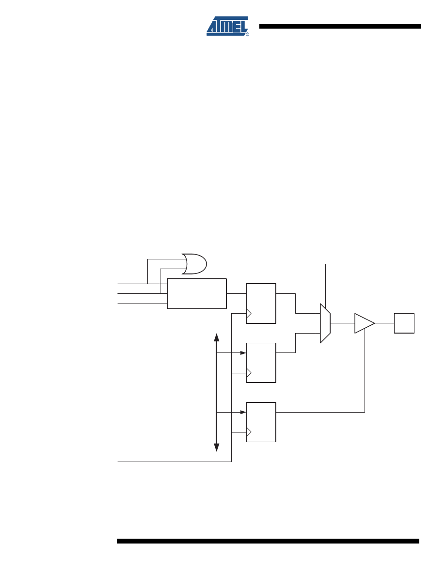
62
2535J–AVR–08/10
ATtiny13
generation. Similarly, do not write the TCNT0 value equal to BOTTOM when the counter is
down-counting.
The setup of the OC0x should be performed before setting the Data Direction Register for the
port pin to output. The easiest way of setting the OC0x value is to use the Force Output Com-
pare (FOC0x) strobe bits in Normal mode. The OC0x Registers keep their values even when
changing between Waveform Generation modes.
Be aware that the COM0x1:0 bits are not double buffered together with the compare value.
Changing the COM0x1:0 bits will take effect immediately.
11.6 Compare Match Output Unit
The Compare Output mode (COM0x1:0) bits have two functions. The Waveform Generator uses
the COM0x1:0 bits for defining the Output Compare (OC0x) state at the next Compare Match.
Also, the COM0x1:0 bits control the OC0x pin output source.
shows a
simplified schematic of the logic affected by the COM0x1:0 bit setting. The I/O Registers, I/O
bits, and I/O pins in the figure are shown in bold. Only the parts of the general I/O Port Control
Registers (DDR and PORT) that are affected by the COM0x1:0 bits are shown. When referring
to the OC0x state, the reference is for the internal OC0x Register, not the OC0x pin. If a system
reset occur, the OC0x Register is reset to “0”.
Figure 11-4. Compare Match Output Unit, Schematic
The general I/O port function is overridden by the Output Compare (OC0x) from the Waveform
Generator if either of the COM0x1:0 bits are set. However, the OC0x pin direction (input or out-
put) is still controlled by the Data Direction Register (DDR) for the port pin. The Data Direction
Register bit for the OC0x pin (DDR_OC0x) must be set as output before the OC0x value is visi-
ble on the pin. The port override function is independent of the Waveform Generation mode.
PORT
DDR
D
Q
D
Q
OCn
Pin
OCnx
D
Q
Waveform
Generator
COMnx1
COMnx0
0
1
D
ATA
B
U
S
FOCn
clk
I/O

63
2535J–AVR–08/10
ATtiny13
The design of the Output Compare pin logic allows initialization of the OC0x state before the out-
put is enabled. Note that some COM0x1:0 bit settings are reserved for certain modes of
operation.
See “Register Description” on page 69.
11.6.1
Compare Output Mode and Waveform Generation
The Waveform Generator uses the COM0x1:0 bits differently in Normal, CTC, and PWM modes.
For all modes, setting the COM0x1:0 = 0 tells the Waveform Generator that no action on the
OC0x Register is to be performed on the next Compare Match. For compare output actions in
the non-PWM modes refer to
, and for phase correct PWM refer to
.
A change of the COM0x1:0 bits state will have effect at the first Compare Match after the bits are
written. For non-PWM modes, the action can be forced to have immediate effect by using the
FOC0x strobe bits.
11.7 Modes of Operation
The mode of operation, i.e., the behavior of the Timer/Counter and the Output Compare pins, is
defined by the combination of the Waveform Generation mode (WGM02:0) and Compare Output
mode (COM0x1:0) bits. The Compare Output mode bits do not affect the counting sequence,
while the Waveform Generation mode bits do. The COM0x1:0 bits control whether the PWM out-
put generated should be inverted or not (inverted or non-inverted PWM). For non-PWM modes
the COM0x1:0 bits control whether the output should be set, cleared, or toggled at a Compare
Match (
See “Compare Match Output Unit” on page 62.
).
For detailed timing information refer to
and
“Timer/Counter Timing Diagrams” on page
.
11.7.1
Normal Mode
The simplest mode of operation is the Normal mode (WGM02:0 = 0). In this mode the counting
direction is always up (incrementing), and no counter clear is performed. The counter simply
overruns when it passes its maximum 8-bit value (TOP = 0xFF) and then restarts from the bot-
tom (0x00). In normal operation the Timer/Counter Overflow Flag (TOV0) will be set in the same
timer clock cycle as the TCNT0 becomes zero. The TOV0 Flag in this case behaves like a ninth
bit, except that it is only set, not cleared. However, combined with the timer overflow interrupt
that automatically clears the TOV0 Flag, the timer resolution can be increased by software.
There are no special cases to consider in the Normal mode, a new counter value can be written
anytime.
The Output Compare Unit can be used to generate interrupts at some given time. Using the Out-
put Compare to generate waveforms in Normal mode is not recommended, since this will
occupy too much of the CPU time.
11.7.2
Clear Timer on Compare Match (CTC) Mode
In Clear Timer on Compare or CTC mode (WGM02:0 = 2), the OCR0A Register is used to
manipulate the counter resolution. In CTC mode the counter is cleared to zero when the counter
value (TCNT0) matches the OCR0A. The OCR0A defines the top value for the counter, hence
also its resolution. This mode allows greater control of the Compare Match output frequency. It
also simplifies the operation of counting external events.
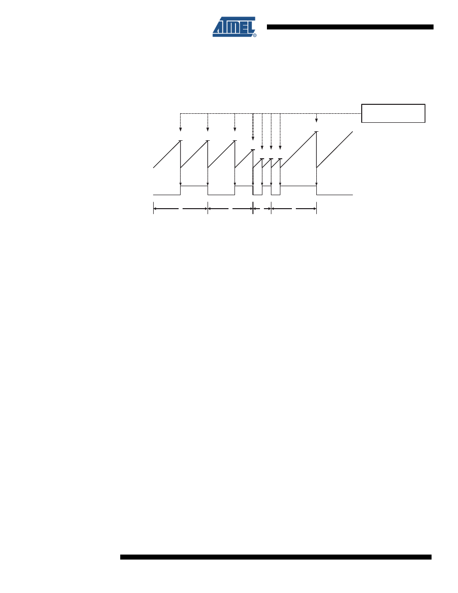
64
2535J–AVR–08/10
ATtiny13
The timing diagram for the CTC mode is shown in
. The counter value
(TCNT0) increases until a Compare Match occurs between TCNT0 and OCR0A, and then coun-
ter (TCNT0) is cleared.
Figure 11-5. CTC Mode, Timing Diagram
An interrupt can be generated each time the counter value reaches the TOP value by using the
OCF0A Flag. If the interrupt is enabled, the interrupt handler routine can be used for updating
the TOP value. However, changing TOP to a value close to BOTTOM when the counter is run-
ning with none or a low prescaler value must be done with care since the CTC mode does not
have the double buffering feature. If the new value written to OCR0A is lower than the current
value of TCNT0, the counter will miss the Compare Match. The counter will then have to count to
its maximum value (0xFF) and wrap around starting at 0x00 before the Compare Match can
occur.
For generating a waveform output in CTC mode, the OC0A output can be set to toggle its logical
level on each Compare Match by setting the Compare Output mode bits to toggle mode
(COM0A1:0 = 1). The OC0A value will not be visible on the port pin unless the data direction for
the pin is set to output. The waveform generated will have a maximum frequency of f
OC0
=
f
clk_I/O
/2 when OCR0A is set to zero (0x00). The waveform frequency is defined by the following
equation:
The N variable represents the prescale factor (1, 8, 64, 256, or 1024).
As for the Normal mode of operation, the TOV0 Flag is set in the same timer clock cycle that the
counter counts from MAX to 0x00.
11.7.3
Fast PWM Mode
The fast Pulse Width Modulation or fast PWM mode (WGM02:0 = 3 or 7) provides a high fre-
quency PWM waveform generation option. The fast PWM differs from the other PWM option by
its single-slope operation. The counter counts from BOTTOM to TOP then restarts from BOT-
TOM. TOP is defined as 0xFF when WGM2:0 = 3, and OCR0A when WGM2:0 = 7. In non-
inverting Compare Output mode, the Output Compare (OC0x) is cleared on the Compare Match
between TCNT0 and OCR0x, and set at BOTTOM. In inverting Compare Output mode, the out-
put is set on Compare Match and cleared at BOTTOM. Due to the single-slope operation, the
operating frequency of the fast PWM mode can be twice as high as the phase correct PWM
mode that use dual-slope operation. This high frequency makes the fast PWM mode well suited
TCNTn
OCn
(Toggle)
OCnx Interrupt Flag Set
1
4
Period
2
3
(COMnx1:0 = 1)
f
OCnx
f
clk_I/O
2 N
1 OCRnx
+
(
)
⋅
⋅
--------------------------------------------------
=
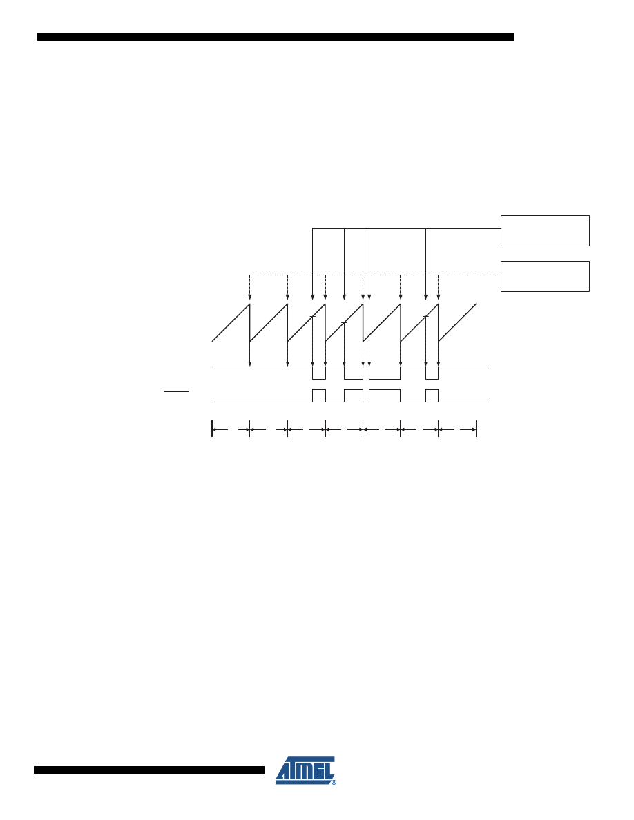
65
2535J–AVR–08/10
ATtiny13
for power regulation, rectification, and DAC applications. High frequency allows physically small
sized external components (coils, capacitors), and therefore reduces total system cost.
In fast PWM mode, the counter is incremented until the counter value matches the TOP value.
The counter is then cleared at the following timer clock cycle. The timing diagram for the fast
PWM mode is shown in
. The TCNT0 value is in the timing diagram
shown as a histogram for illustrating the single-slope operation. The diagram includes non-
inverted and inverted PWM outputs. The small horizontal line marks on the TCNT0 slopes repre-
sent Compare Matches between OCR0x and TCNT0.
Figure 11-6. Fast PWM Mode, Timing Diagram
The Timer/Counter Overflow Flag (TOV0) is set each time the counter reaches TOP. If the inter-
rupt is enabled, the interrupt handler routine can be used for updating the compare value.
In fast PWM mode, the compare unit allows generation of PWM waveforms on the OC0x pins.
Setting the COM0x1:0 bits to two will produce a non-inverted PWM and an inverted PWM output
can be generated by setting the COM0x1:0 to three: Setting the COM0A1:0 bits to one allows
the AC0A pin to toggle on Compare Matches if the WGM02 bit is set. This option is not available
for the OC0B pin (See
). The actual OC0x value will only be visible on the
port pin if the data direction for the port pin is set as output. The PWM waveform is generated by
setting (or clearing) the OC0x Register at the Compare Match between OCR0x and TCNT0, and
clearing (or setting) the OC0x Register at the timer clock cycle the counter is cleared (changes
from TOP to BOTTOM).
The PWM frequency for the output can be calculated by the following equation:
The N variable represents the prescale factor (1, 8, 64, 256, or 1024).
The extreme values for the OCR0A Register represents special cases when generating a PWM
waveform output in the fast PWM mode. If the OCR0A is set equal to BOTTOM, the output will
be a narrow spike for each MAX+1 timer clock cycle. Setting the OCR0A equal to MAX will result
TCNTn
OCRnx Update and
TOVn Interrupt Flag Set
1
Period
2
3
OCn
OCn
(COMnx1:0 = 2)
(COMnx1:0 = 3)
OCRnx Interrupt Flag Set
4
5
6
7
f
OCnxPWM
f
clk_I/O
N 256
⋅
------------------
=
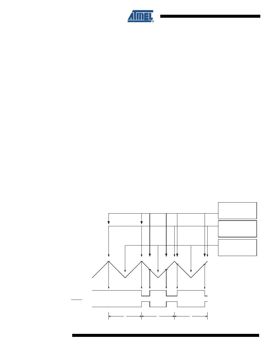
66
2535J–AVR–08/10
ATtiny13
in a constantly high or low output (depending on the polarity of the output set by the COM0A1:0
bits.)
A frequency (with 50% duty cycle) waveform output in fast PWM mode can be achieved by set-
ting OC0x to toggle its logical level on each Compare Match (COM0x1:0 = 1). The waveform
generated will have a maximum frequency of f
OC0
= f
clk_I/O
/2 when OCR0A is set to zero. This
feature is similar to the OC0A toggle in CTC mode, except the double buffer feature of the Out-
put Compare unit is enabled in the fast PWM mode.
11.7.4
Phase Correct PWM Mode
The phase correct PWM mode (WGM02:0 = 1 or 5) provides a high resolution phase correct
PWM waveform generation option. The phase correct PWM mode is based on a dual-slope
operation. The counter counts repeatedly from BOTTOM to TOP and then from TOP to BOT-
TOM. TOP is defined as 0xFF when WGM2:0 = 1, and OCR0A when WGM2:0 = 5. In non-
inverting Compare Output mode, the Output Compare (OC0x) is cleared on the Compare Match
between TCNT0 and OCR0x while upcounting, and set on the Compare Match while down-
counting. In inverting Output Compare mode, the operation is inverted. The dual-slope operation
has lower maximum operation frequency than single slope operation. However, due to the sym-
metric feature of the dual-slope PWM modes, these modes are preferred for motor control
applications.
In phase correct PWM mode the counter is incremented until the counter value matches TOP.
When the counter reaches TOP, it changes the count direction. The TCNT0 value will be equal
to TOP for one timer clock cycle. The timing diagram for the phase correct PWM mode is shown
on
. The TCNT0 value is in the timing diagram shown as a histogram for
illustrating the dual-slope operation. The diagram includes non-inverted and inverted PWM out-
puts. The small horizontal line marks on the TCNT0 slopes represent Compare Matches
between OCR0x and TCNT0.
Figure 11-7. Phase Correct PWM Mode, Timing Diagram
TOVn Interrupt Flag Set
OCnx Interrupt Flag Set
1
2
3
TCNTn
Period
OCn
OCn
(COMnx1:0 = 2)
(COMnx1:0 = 3)
OCRnx Update

67
2535J–AVR–08/10
ATtiny13
The Timer/Counter Overflow Flag (TOV0) is set each time the counter reaches BOTTOM. The
Interrupt Flag can be used to generate an interrupt each time the counter reaches the BOTTOM
value.
In phase correct PWM mode, the compare unit allows generation of PWM waveforms on the
OC0x pins. Setting the COM0x1:0 bits to two will produce a non-inverted PWM. An inverted
PWM output can be generated by setting the COM0x1:0 to three: Setting the COM0A0 bits to
one allows the OC0A pin to toggle on Compare Matches if the WGM02 bit is set. This option is
not available for the OC0B pin (See
). The actual OC0x value will only be
visible on the port pin if the data direction for the port pin is set as output. The PWM waveform is
generated by clearing (or setting) the OC0x Register at the Compare Match between OCR0x
and TCNT0 when the counter increments, and setting (or clearing) the OC0x Register at Com-
pare Match between OCR0x and TCNT0 when the counter decrements. The PWM frequency for
the output when using phase correct PWM can be calculated by the following equation:
The N variable represents the prescale factor (1, 8, 64, 256, or 1024).
The extreme values for the OCR0A Register represent special cases when generating a PWM
waveform output in the phase correct PWM mode. If the OCR0A is set equal to BOTTOM, the
output will be continuously low and if set equal to MAX the output will be continuously high for
non-inverted PWM mode. For inverted PWM the output will have the opposite logic values.
At the very start of period 2 in
OCn has a transition from high to low
even though there is no Compare Match. The point of this transition is to guarantee symmetry
around BOTTOM. There are two cases that give a transition without Compare Match.
• OCR0A changes its value from MAX, like in
. When the OCR0A value
is MAX the OCn pin value is the same as the result of a down-counting Compare Match. To
ensure symmetry around BOTTOM the OCn value at MAX must correspond to the result of
an up-counting Compare Match.
• The timer starts counting from a value higher than the one in OCR0A, and for that reason
misses the Compare Match and hence the OCn change that would have happened on the
way up.
11.8 Timer/Counter Timing Diagrams
The Timer/Counter is a synchronous design and the timer clock (clk
T0
) is therefore shown as a
clock enable signal in the following figures. The figures include information on when Interrupt
Flags are set.
contains timing data for basic Timer/Counter operation.
The figure shows the count sequence close to the MAX value in all modes other than phase cor-
rect PWM mode.
f
OCnxPCPWM
f
clk_I/O
N 510
⋅
------------------
=
68
2535J–AVR–08/10
ATtiny13
Figure 11-8. Timer/Counter Timing Diagram, no Prescaling
shows the same timing data, but with the prescaler enabled.
Figure 11-9. Timer/Counter Timing Diagram, with Prescaler (f
clk_I/O
/8)
shows the setting of OCF0B in all modes and OCF0A in all modes except CTC
mode and PWM mode, where OCR0A is TOP.
Figure 11-10. Timer/Counter Timing Diagram, Setting of OCF0x, with Prescaler (f
clk_I/O
/8)
shows the setting of OCF0A and the clearing of TCNT0 in CTC mode
and fast PWM mode where OCR0A is TOP.
clk
Tn
(clk
I/O
/1)
TOVn
clk
I/O
TCNTn
MAX - 1
MAX
BOTTOM
BOTTOM + 1
TOVn
TCNTn
MAX - 1
MAX
BOTTOM
BOTTOM + 1
clk
I/O
clk
Tn
(clk
I/O
/8)
OCFnx
OCRnx
TCNTn
OCRnx Value
OCRnx - 1
OCRnx
OCRnx + 1
OCRnx + 2
clk
I/O
clk
Tn
(clk
I/O
/8)
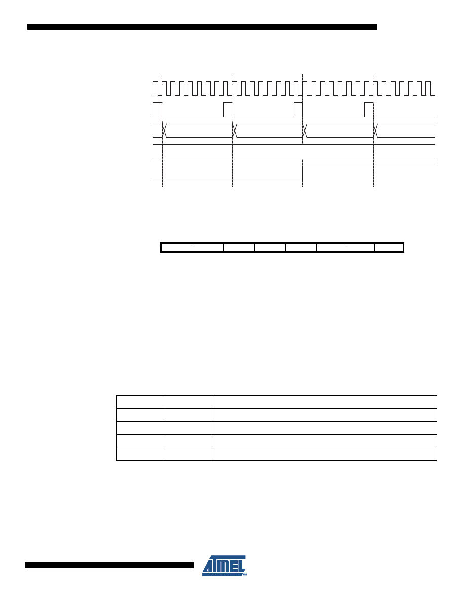
69
2535J–AVR–08/10
ATtiny13
Figure 11-11. Timer/Counter Timing Diagram, Clear Timer on Compare Match mode, with Pres-
caler (f
clk_I/O
/8)
11.9 Register Description
11.9.1
TCCR0A – Timer/Counter Control Register A
• Bits 7:6 – COM01A:0: Compare Match Output A Mode
These bits control the Output Compare pin (OC0A) behavior. If one or both of the COM0A1:0
bits are set, the OC0A output overrides the normal port functionality of the I/O pin it is connected
to. However, note that the Data Direction Register (DDR) bit corresponding to the OC0A pin
must be set in order to enable the output driver.
When OC0A is connected to the pin, the function of the COM0A1:0 bits depends on the
WGM02:0 bit setting.
shows the COM0A1:0 bit functionality when the WGM02:0 bits are set to a normal or
CTC mode (non-PWM).
shows the COM0A1:0 bit functionality when the WGM01:0 bits are set to
fast PWM mode.
OCFnx
OCRnx
TCNTn
(CTC)
TOP
TOP - 1
TOP
BOTTOM
BOTTOM + 1
clk
I/O
clk
Tn
(clk
I/O
/8)
Bit
7
6
5
4
3
2
1
0
COM0A1
COM0A0
COM0B1
COM0B0
–
–
WGM01
WGM00
TCCR0A
Read/Write
R/W
R/W
R/W
R/W
R
R
R/W
R/W
Initial Value
0
0
0
0
0
0
0
0
Table 11-2.
Compare Output Mode, non-PWM Mode
COM01
COM00
Description
0
0
Normal port operation, OC0A disconnected.
0
1
Toggle OC0A on Compare Match
1
0
Clear OC0A on Compare Match
1
1
Set OC0A on Compare Match

70
2535J–AVR–08/10
ATtiny13
Note:
1. A special case occurs when OCR0A equals TOP and COM0A1 is set. In this case, the Com-
pare Match is ignored, but the set or clear is done at TOP. See
for more details.
shows the COM0A1:0 bit functionality when the WGM02:0 bits are set to phase cor-
rect PWM mode.
Note:
1. A special case occurs when OCR0A equals TOP and COM0A1 is set. In this case, the Com-
pare Match is ignored, but the set or clear is done at TOP. See
• Bits 5:4 – COM0B1:0: Compare Match Output B Mode
These bits control the Output Compare pin (OC0B) behavior. If one or both of the COM0B1:0
bits are set, the OC0B output overrides the normal port functionality of the I/O pin it is connected
to. However, note that the Data Direction Register (DDR) bit corresponding to the OC0B pin
must be set in order to enable the output driver.
When OC0B is connected to the pin, the function of the COM0B1:0 bits depends on the
WGM02:0 bit setting.
shows the COM0B1:0 bit functionality when the WGM02:0 bits are set to
a normal or CTC mode (non-PWM).
Table 11-3.
Compare Output Mode, Fast PWM Mode
COM01
COM00
Description
0
0
Normal port operation, OC0A disconnected.
0
1
WGM02 = 0: Normal Port Operation, OC0A Disconnected.
WGM02 = 1: Toggle OC0A on Compare Match.
1
0
Clear OC0A on Compare Match, set OC0A at TOP
1
1
Set OC0A on Compare Match, clear OC0A at TOP
Table 11-4.
Compare Output Mode, Phase Correct PWM Mode
COM0A1
COM0A0
Description
0
0
Normal port operation, OC0A disconnected.
0
1
WGM02 = 0: Normal Port Operation, OC0A Disconnected.
WGM02 = 1: Toggle OC0A on Compare Match.
1
0
Clear OC0A on Compare Match when up-counting. Set OC0A on
Compare Match when down-counting.
1
1
Set OC0A on Compare Match when up-counting. Clear OC0A on
Compare Match when down-counting.
71
2535J–AVR–08/10
ATtiny13
shows the COM0B1:0 bit functionality when the WGM02:0 bits are set to fast PWM
mode.
Note:
1. A special case occurs when OCR0B equals TOP and COM0B1 is set. In this case, the Com-
pare Match is ignored, but the set or clear is done at TOP. See
for more details.
shows the COM0B1:0 bit functionality when the WGM02:0 bits are set to phase cor-
rect PWM mode.
Note:
1. A special case occurs when OCR0B equals TOP and COM0B1 is set. In this case, the Com-
pare Match is ignored, but the set or clear is done at TOP. See
• Bits 3, 2 – Res: Reserved Bits
These bits are reserved bits in the ATtiny13 and will always read as zero.
Table 11-5.
Compare Output Mode, non-PWM Mode
COM01
COM00
Description
0
0
Normal port operation, OC0B disconnected.
0
1
Toggle OC0B on Compare Match
1
0
Clear OC0B on Compare Match
1
1
Set OC0B on Compare Match
Table 11-6.
Compare Output Mode, Fast PWM Mode
COM01
COM00
Description
0
0
Normal port operation, OC0B disconnected.
0
1
Reserved
1
0
Clear OC0B on Compare Match, set OC0B at TOP
1
1
Set OC0B on Compare Match, clear OC0B at TOP
Table 11-7.
Compare Output Mode, Phase Correct PWM Mode
COM0A1
COM0A0
Description
0
0
Normal port operation, OC0B disconnected.
0
1
Reserved
1
0
Clear OC0B on Compare Match when up-counting. Set OC0B on
Compare Match when down-counting.
1
1
Set OC0B on Compare Match when up-counting. Clear OC0B on
Compare Match when down-counting.

72
2535J–AVR–08/10
ATtiny13
• Bits 1:0 – WGM01:0: Waveform Generation Mode
Combined with the WGM02 bit found in the TCCR0B Register, these bits control the counting
sequence of the counter, the source for maximum (TOP) counter value, and what type of wave-
form generation to be used, see
. Modes of operation supported by the
Timer/Counter unit are: Normal mode (counter), Clear Timer on Compare Match (CTC) mode,
and two types of Pulse Width Modulation (PWM) modes (see
“Modes of Operation” on page 63
Notes: 1. MAX = 0xFF
2. BOTTOM = 0x00
11.9.2
TCCR0B – Timer/Counter Control Register B
• Bit 7 – FOC0A: Force Output Compare A
The FOC0A bit is only active when the WGM bits specify a non-PWM mode.
However, for ensuring compatibility with future devices, this bit must be set to zero when
TCCR0B is written when operating in PWM mode. When writing a logical one to the FOC0A bit,
an immediate Compare Match is forced on the Waveform Generation unit. The OC0A output is
changed according to its COM0A1:0 bits setting. Note that the FOC0A bit is implemented as a
strobe. Therefore it is the value present in the COM0A1:0 bits that determines the effect of the
forced compare.
A FOC0A strobe will not generate any interrupt, nor will it clear the timer in CTC mode using
OCR0A as TOP.
The FOC0A bit is always read as zero.
Table 11-8.
Waveform Generation Mode Bit Description
Mode
WGM2
WGM1
WGM0
Timer/Counter
Mode of
Operation
TOP
Update of
OCRx at
TOV Flag
Set on
0
0
0
0
Normal
0xFF
Immediate
MAX
1
0
0
1
PWM
(Phase Correct)
0xFF
TOP
BOTTOM
2
0
1
0
CTC
OCRA
Immediate
MAX
3
0
1
1
Fast PWM
0xFF
TOP
MAX
4
1
0
0
Reserved
–
–
–
5
1
0
1
PWM
(Phase Correct)
OCRA
TOP
BOTTOM
6
1
1
0
Reserved
–
–
–
7
1
1
1
Fast PWM
OCRA
TOP
TOP
Bit
7
6
5
4
3
2
1
0
FOC0A
FOC0B
–
–
WGM02
CS02
CS01
CS00
TCCR0B
Read/Write
W
W
R
R
R/W
R/W
R/W
R/W
Initial Value
0
0
0
0
0
0
0
0

73
2535J–AVR–08/10
ATtiny13
• Bit 6 – FOC0B: Force Output Compare B
The FOC0B bit is only active when the WGM bits specify a non-PWM mode.
However, for ensuring compatibility with future devices, this bit must be set to zero when
TCCR0B is written when operating in PWM mode. When writing a logical one to the FOC0B bit,
an immediate Compare Match is forced on the Waveform Generation unit. The OC0B output is
changed according to its COM0B1:0 bits setting. Note that the FOC0B bit is implemented as a
strobe. Therefore it is the value present in the COM0B1:0 bits that determines the effect of the
forced compare.
A FOC0B strobe will not generate any interrupt, nor will it clear the timer in CTC mode using
OCR0B as TOP.
The FOC0B bit is always read as zero.
• Bits 5:4 – Res: Reserved Bits
These bits are reserved bits in the ATtiny13 and will always read as zero.
• Bit 3 – WGM02: Waveform Generation Mode
See the description in the
“TCCR0A – Timer/Counter Control Register A” on page 69
.
• Bits 2:0 – CS02:0: Clock Select
The three Clock Select bits select the clock source to be used by the Timer/Counter.
If external pin modes are used for the Timer/Counter0, transitions on the T0 pin will clock the
counter even if the pin is configured as an output. This feature allows software control of the
counting.
11.9.3
TCNT0 – Timer/Counter Register
The Timer/Counter Register gives direct access, both for read and write operations, to the
Timer/Counter unit 8-bit counter. Writing to the TCNT0 Register blocks (removes) the Compare
Match on the following timer clock. Modifying the counter (TCNT0) while the counter is running,
introduces a risk of missing a Compare Match between TCNT0 and the OCR0x Registers.
Table 11-9.
Clock Select Bit Description
CS02
CS01
CS00
Description
0
0
0
No clock source (Timer/Counter stopped)
0
0
1
clk
I/O
/(No prescaling)
0
1
0
clk
I/O
/8 (From prescaler)
0
1
1
clk
I/O
/64 (From prescaler)
1
0
0
clk
I/O
/256 (From prescaler)
1
0
1
clk
I/O
/1024 (From prescaler)
1
1
0
External clock source on T0 pin. Clock on falling edge.
1
1
1
External clock source on T0 pin. Clock on rising edge.
Bit
7
6
5
4
3
2
1
0
TCNT0[7:0]
TCNT0
Read/Write
R/W
R/W
R/W
R/W
R/W
R/W
R/W
R/W
Initial Value
0
0
0
0
0
0
0
0

74
2535J–AVR–08/10
ATtiny13
11.9.4
OCR0A – Output Compare Register A
The Output Compare Register A contains an 8-bit value that is continuously compared with the
counter value (TCNT0). A match can be used to generate an Output Compare interrupt, or to
generate a waveform output on the OC0A pin.
11.9.5
OCR0B – Output Compare Register B
The Output Compare Register B contains an 8-bit value that is continuously compared with the
counter value (TCNT0). A match can be used to generate an Output Compare interrupt, or to
generate a waveform output on the OC0B pin.
11.9.6
TIMSK0 – Timer/Counter Interrupt Mask Register
• Bits 7:4, 0 – Res: Reserved Bits
These bits are reserved bits in the ATtiny13 and will always read as zero.
• Bit 3 – OCIE0B: Timer/Counter Output Compare Match B Interrupt Enable
When the OCIE0B bit is written to one, and the I-bit in the Status Register is set, the
Timer/Counter Compare Match B interrupt is enabled. The corresponding interrupt is executed if
a Compare Match in Timer/Counter occurs, i.e., when the OCF0B bit is set in the Timer/Counter
Interrupt Flag Register – TIFR0.
• Bit 2 – OCIE0A: Timer/Counter0 Output Compare Match A Interrupt Enable
When the OCIE0A bit is written to one, and the I-bit in the Status Register is set, the
Timer/Counter0 Compare Match A interrupt is enabled. The corresponding interrupt is executed
if a Compare Match in Timer/Counter0 occurs, i.e., when the OCF0A bit is set in the
Timer/Counter 0 Interrupt Flag Register – TIFR0.
• Bit 1 – TOIE0: Timer/Counter0 Overflow Interrupt Enable
When the TOIE0 bit is written to one, and the I-bit in the Status Register is set, the
Timer/Counter0 Overflow interrupt is enabled. The corresponding interrupt is executed if an
overflow in Timer/Counter0 occurs, i.e., when the TOV0 bit is set in the Timer/Counter 0 Inter-
rupt Flag Register – TIFR0.
Bit
7
6
5
4
3
2
1
0
OCR0A[7:0]
OCR0A
Read/Write
R/W
R/W
R/W
R/W
R/W
R/W
R/W
R/W
Initial Value
0
0
0
0
0
0
0
0
Bit
7
6
5
4
3
2
1
0
OCR0B[7:0]
OCR0B
Read/Write
R/W
R/W
R/W
R/W
R/W
R/W
R/W
R/W
Initial Value
0
0
0
0
0
0
0
0
Bit
7
6
5
4
3
2
1
0
–
–
–
–
OCIE0B
OCIE0A
TOIE0
–
TIMSK0
Read/Write
R
R
R
R
R/W
R/W
R/W
R
Initial Value
0
0
0
0
0
0
0
0

75
2535J–AVR–08/10
ATtiny13
11.9.7
TIFR0 – Timer/Counter 0 Interrupt Flag Register
• Bits 7:4, 0 – Res: Reserved Bits
These bits are reserved bits in the ATtiny13 and will always read as zero.
• Bit 3 – OCF0B: Output Compare Flag 0 B
The OCF0B bit is set when a Compare Match occurs between the Timer/Counter and the data in
OCR0B – Output Compare Register0 B. OCF0B is cleared by hardware when executing the cor-
responding interrupt handling vector. Alternatively, OCF0B is cleared by writing a logic one to
the flag. When the I-bit in SREG, OCIE0B (Timer/Counter Compare B Match Interrupt Enable),
and OCF0B are set, the Timer/Counter Compare Match Interrupt is executed.
• Bit 2 – OCF0A: Output Compare Flag 0 A
The OCF0A bit is set when a Compare Match occurs between the Timer/Counter0 and the data
in OCR0A – Output Compare Register0. OCF0A is cleared by hardware when executing the cor-
responding interrupt handling vector. Alternatively, OCF0A is cleared by writing a logic one to
the flag. When the I-bit in SREG, OCIE0A (Timer/Counter0 Compare Match Interrupt Enable),
and OCF0A are set, the Timer/Counter0 Compare Match Interrupt is executed.
• Bit 1 – TOV0: Timer/Counter0 Overflow Flag
The bit TOV0 is set when an overflow occurs in Timer/Counter0. TOV0 is cleared by hardware
when executing the corresponding interrupt handling vector. Alternatively, TOV0 is cleared by
writing a logic one to the flag. When the SREG I-bit, TOIE0 (Timer/Counter0 Overflow Interrupt
Enable), and TOV0 are set, the Timer/Counter0 Overflow interrupt is executed.
The setting of this flag is dependent of the WGM02:0 bit setting. Refer to
Generation Mode Bit Description” on page 72
.
Bit
7
6
5
4
3
2
1
0
–
–
–
–
OCF0B
OCF0A
TOV0
–
TIFR0
Read/Write
R
R
R
R
R/W
R/W
R/W
R
Initial Value
0
0
0
0
0
0
0
0
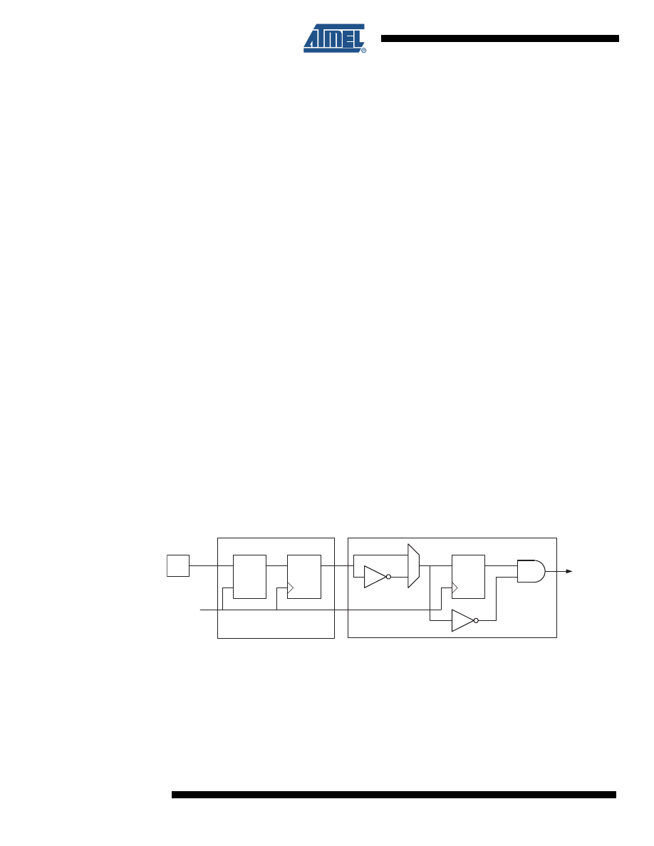
76
2535J–AVR–08/10
ATtiny13
12. Timer/Counter Prescaler
12.1 Overview
The Timer/Counter can be clocked directly by the system clock (by setting the CSn2:0 = 1). This
provides the fastest operation, with a maximum Timer/Counter clock frequency equal to system
clock frequency (f
CLK_I/O
). Alternatively, one of four taps from the prescaler can be used as a
clock source. The prescaled clock has a frequency of either f
CLK_I/O
/8, f
CLK_I/O
/64, f
CLK_I/O
/256, or
f
CLK_I/O
/1024.
12.2 Prescaler Reset
The prescaler is free running, i.e., operates independently of the Clock Select logic of the
Timer/Counter. Since the prescaler is not affected by the Timer/Counter’s clock select, the state
of the prescaler will have implications for situations where a prescaled clock is used. One exam-
ple of prescaling artifacts occurs when the timer is enabled and clocked by the prescaler (6 >
CSn2:0 > 1). The number of system clock cycles from when the timer is enabled to the first count
occurs can be from 1 to N+1 system clock cycles, where N equals the prescaler divisor (8, 64,
256, or 1024).
It is possible to use the Prescaler Reset for synchronizing the Timer/Counter to program
execution.
12.3 External Clock Source
An external clock source applied to the T0 pin can be used as Timer/Counter clock (clk
T0
). The
T0 pin is sampled once every system clock cycle by the pin synchronization logic. The synchro-
nized (sampled) signal is then passed through the edge detector.
a functional equivalent block diagram of the T0 synchronization and edge detector logic. The
registers are clocked at the positive edge of the internal system clock (
clk
I/O
). The latch is trans-
parent in the high period of the internal system clock.
The edge detector generates one clk
T
0
pulse for each positive (CSn2:0 = 7) or negative (CSn2:0
= 6) edge it detects.
Figure 12-1. T0 Pin Sampling
The synchronization and edge detector logic introduces a delay of 2.5 to 3.5 system clock cycles
from an edge has been applied to the T0 pin to the counter is updated.
Enabling and disabling of the clock input must be done when T0 has been stable for at least one
system clock cycle, otherwise it is a risk that a false Timer/Counter clock pulse is generated.
Each half period of the external clock applied must be longer than one system clock cycle to
ensure correct sampling. The external clock must be guaranteed to have less than half the sys-
tem clock frequency (f
ExtClk
< f
clk_I/O
/2) given a 50/50% duty cycle. Since the edge detector uses
Tn_sync
(To Clock
Select Logic)
Edge Detector
Synchronization
D
Q
D
Q
LE
D
Q
Tn
clk
I/O
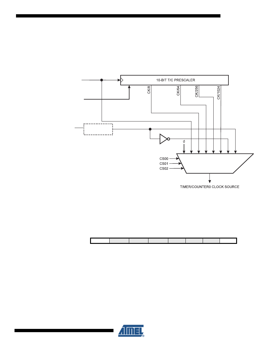
77
2535J–AVR–08/10
ATtiny13
sampling, the maximum frequency of an external clock it can detect is half the sampling fre-
quency (Nyquist sampling theorem). However, due to variation of the system clock frequency
and duty cycle caused by Oscillator source (crystal, resonator, and capacitors) tolerances, it is
recommended that maximum frequency of an external clock source is less than f
clk_I/O
/2.5.
An external clock source can not be prescaled.
Figure 12-2. Prescaler for Timer/Counter0
Note:
1. The synchronization logic on the input pins (
T0)
is shown in
.
12.4 Register Description.
12.4.1
GTCCR – General Timer/Counter Control Register
• Bit 7 – TSM: Timer/Counter Synchronization Mode
Writing the TSM bit to one activates the Timer/Counter Synchronization mode. In this mode, the
value that is written to the PSR10 bit is kept, hence keeping the Prescaler Reset signal asserted.
This ensures that the Timer/Counter is halted and can be configured without the risk of advanc-
ing during configuration. When the TSM bit is written to zero, the PSR10 bit is cleared by
hardware, and the Timer/Counter start counting.
• Bit 0 – PSR10: Prescaler Reset Timer/Counter0
When this bit is one, the Timer/Counter0 prescaler will be Reset. This bit is normally cleared
immediately by hardware, except if the TSM bit is set.
PSR10
Clear
clk
T0
T0
clk
I/O
Synchronization
Bit
7
6
5
4
3
2
1
0
TSM
–
–
–
–
–
–
PSR10
GTCCR
Read/Write
R/W
R
R
R
R
R
R
R/W
Initial Value
0
0
0
0
0
0
0
0
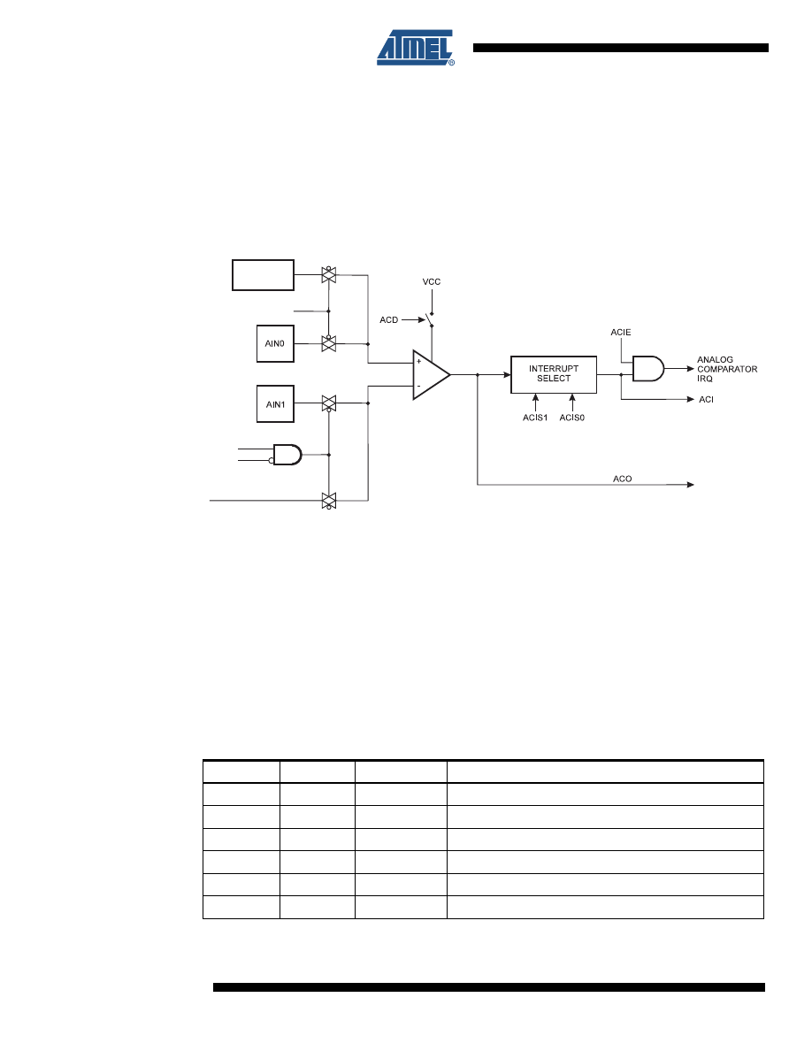
78
2535J–AVR–08/10
ATtiny13
13. Analog Comparator
The Analog Comparator compares the input values on the positive pin AIN0 and negative pin
AIN1. When the voltage on the positive pin AIN0 is higher than the voltage on the negative pin
AIN1, the Analog Comparator output, ACO, is set. The comparator can trigger a separate inter-
rupt, exclusive to the Analog Comparator. The user can select Interrupt triggering on comparator
output rise, fall or toggle. A block diagram of the comparator and its surrounding logic is shown
in
.
Figure 13-1. Analog Comparator Block Diagram
, and
for Analog Compar-
ator pin placement.
13.1 Analog Comparator Multiplexed Input
It is possible to select any of the ADC3..0 pins to replace the negative input to the Analog Com-
parator. The ADC multiplexer is used to select this input, and consequently, the ADC must be
switched off to utilize this feature. If the Analog Comparator Multiplexer Enable bit (ACME in
ADCSRB) is set and the ADC is switched off (ADEN in ADCSRA is zero), MUX1:0 in ADMUX
select the input pin to replace the negative input to the Analog Comparator, as shown in
. If ACME is cleared or ADEN is set, AIN1 is applied to the negative input to the Analog
Comparator.
ACBG
BANDGAP
REFERENCE
ADC MULTIPLEXER
OUTPUT
ACME
ADEN
(1)
Table 13-1.
Analog Comparator Multiplexed Input
ACME
ADEN
MUX1..0
Analog Comparator Negative Input
0
x
xx
AIN1
1
1
xx
AIN1
1
0
00
ADC0
1
0
01
ADC1
1
0
10
ADC2
1
0
11
ADC3

79
2535J–AVR–08/10
ATtiny13
13.2 Register Description
13.2.1
ADCSRB – ADC Control and Status Register
• Bit 6 – ACME: Analog Comparator Multiplexer Enable
When this bit is written logic one and the ADC is switched off (ADEN in ADCSRA is zero), the
ADC multiplexer selects the negative input to the Analog Comparator. When this bit is written
logic zero, AIN1 is applied to the negative input of the Analog Comparator. For a detailed
description of this bit, see
“Analog Comparator Multiplexed Input” on page 78
.
13.2.2
ACSR– Analog Comparator Control and Status Register
• Bit 7 – ACD: Analog Comparator Disable
When this bit is written logic one, the power to the Analog Comparator is switched off. This bit
can be set at any time to turn off the Analog Comparator. This will reduce power consumption in
Active and Idle mode. When changing the ACD bit, the Analog Comparator Interrupt must be
disabled by clearing the ACIE bit in ACSR. Otherwise an interrupt can occur when the bit is
changed.
• Bit 6 – ACBG: Analog Comparator Bandgap Select
When this bit is set, a fixed bandgap reference voltage replaces the positive input to the Analog
Comparator. When this bit is cleared, AIN0 is applied to the positive input of the Analog Compar-
ator. When the bandgap reference is used as input to the Analog Comparator, it will take certain
time for the voltage to stabilize. If not stabilized, the first value may give a wrong value.
• Bit 5 – ACO: Analog Comparator Output
The output of the Analog Comparator is synchronized and then directly connected to ACO. The
synchronization introduces a delay of 1 - 2 clock cycles.
• Bit 4 – ACI: Analog Comparator Interrupt Flag
This bit is set by hardware when a comparator output event triggers the interrupt mode defined
by ACIS1 and ACIS0. The Analog Comparator interrupt routine is executed if the ACIE bit is set
and the I-bit in SREG is set. ACI is cleared by hardware when executing the corresponding inter-
rupt handling vector. Alternatively, ACI is cleared by writing a logic one to the flag.
• Bit 3 – ACIE: Analog Comparator Interrupt Enable
When the ACIE bit is written logic one and the I-bit in the Status Register is set, the Analog Com-
parator interrupt is activated. When written logic zero, the interrupt is disabled.
• Bit 2 – Res: Reserved Bit
This bit is a reserved bit in the ATtiny13 and will always read as zero.
Bit
7
6
5
4
3
2
1
0
–
ACME
–
–
–
ADTS2
ADTS1
ADTS0
ADCSRB
Read/Write
R
R/W
R
R
R
R/W
R/W
R/W
Initial Value
0
0
0
0
0
0
0
0
Bit
7
6
5
4
3
2
1
0
ACD
ACBG
ACO
ACI
ACIE
–
ACIS1
ACIS0
ACSR
Read/Write
R/W
R/W
R
R/W
R/W
R
R/W
R/W
Initial Value
0
0
N/A
0
0
0
0
0
80
2535J–AVR–08/10
ATtiny13
• Bits 1, 0 – ACIS1, ACIS0: Analog Comparator Interrupt Mode Select
These bits determine which comparator events that trigger the Analog Comparator interrupt. The
different settings are shown in
When changing the ACIS1/ACIS0 bits, the Analog Comparator Interrupt must be disabled by
clearing its Interrupt Enable bit in the ACSR Register. Otherwise an interrupt can occur when the
bits are changed.
13.2.3
DIDR0 – Digital Input Disable Register 0
• Bits 1, 0 – AIN1D, AIN0D: AIN1, AIN0 Digital Input Disable
When this bit is written logic one, the digital input buffer on the AIN1/0 pin is disabled. The corre-
sponding PIN Register bit will always read as zero when this bit is set. When an analog signal is
applied to the AIN1/0 pin and the digital input from this pin is not needed, this bit should be writ-
ten logic one to reduce power consumption in the digital input buffer.
Table 13-2.
ACIS1/ACIS0 Settings
ACIS1
ACIS0
Interrupt Mode
0
0
Comparator Interrupt on Output Toggle.
0
1
Reserved
1
0
Comparator Interrupt on Falling Output Edge.
1
1
Comparator Interrupt on Rising Output Edge.
Bit
7
6
5
4
3
2
1
0
–
–
ADC0D
ADC2D
ADC3D
ADC1D
AIN1D
AIN0D
DIDR0
Read/Write
R
R
R/W
R/W
R/W
R/W
R/W
R/W
Initial Value
0
0
0
0
0
0
0
0
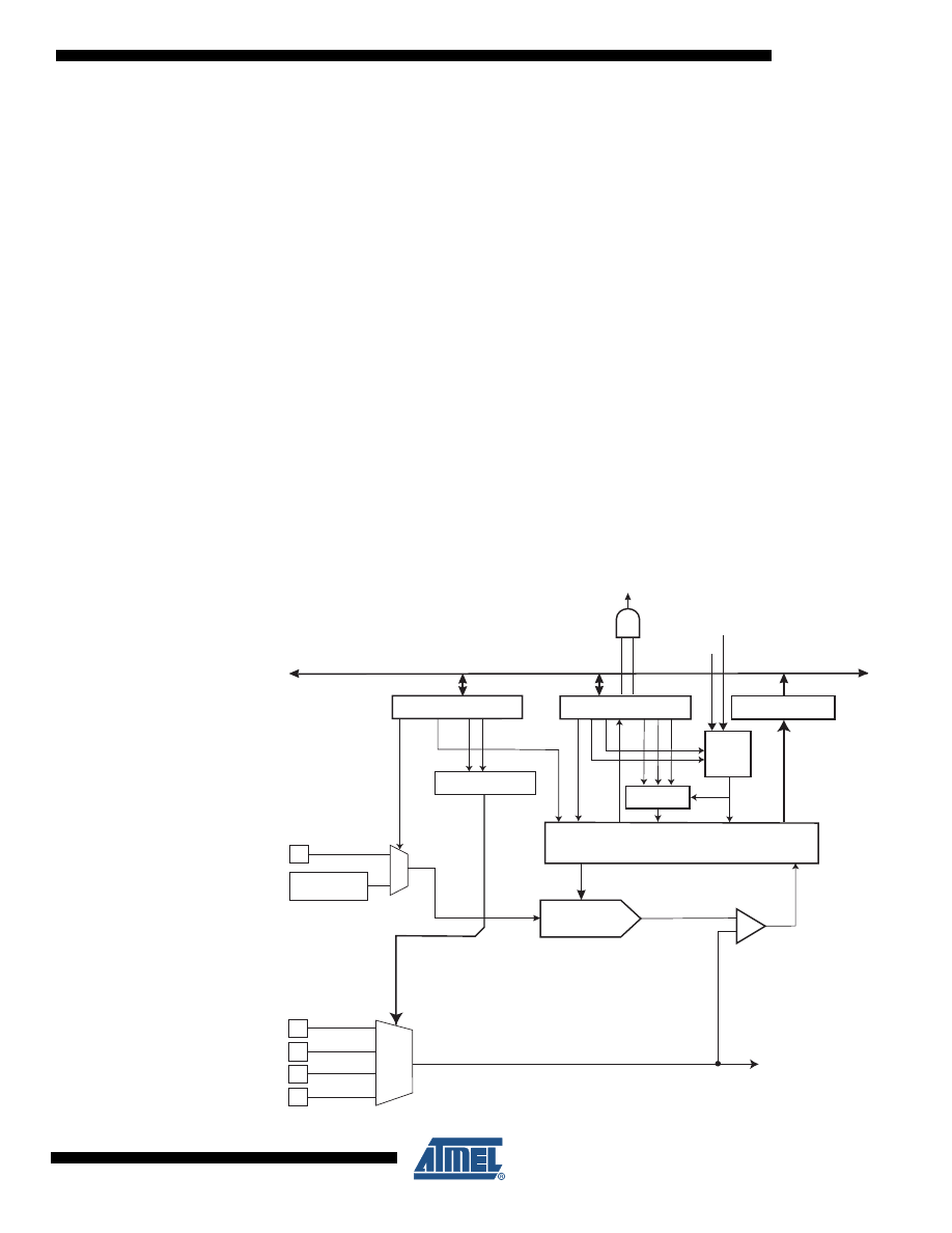
81
2535J–AVR–08/10
ATtiny13
14. Analog to Digital Converter
14.1 Features
•
10-bit Resolution
•
0.5 LSB Integral Non-linearity
•
± 2 LSB Absolute Accuracy
•
13 - 260 µs Conversion Time
•
Up to 15 kSPS at Maximum Resolution
•
Four Multiplexed Single Ended Input Channels
•
Optional Left Adjustment for ADC Result Readout
•
0 - V
CC
ADC Input Voltage Range
•
Selectable 1.1V ADC Reference Voltage
•
Free Running or Single Conversion Mode
•
ADC Start Conversion by Auto Triggering on Interrupt Sources
•
Interrupt on ADC Conversion Complete
•
Sleep Mode Noise Canceler
14.2 Overview
The ATtiny13 features a 10-bit successive approximation ADC. A block diagram of the ADC is
shown in
.
Figure 14-1. Analog to Digital Converter Block Schematic
ADC CONVERSION
COMPLETE IRQ
8-BIT DATA BUS
15
0
ADC MULTIPLEXER
SELECT (ADMUX)
ADC CTRL. & STATUS
REGISTER (ADCSRA)
ADC DATA REGISTER
(ADCH/ADCL)
ADIE
ADATE
ADSC
ADEN
ADIF
ADIF
MUX1
MUX0
ADPS0
ADPS1
ADPS2
CONVERSION LOGIC
10-BIT DAC
+
-
SAMPLE & HOLD
COMPARATOR
INTERNAL 1.1V
REFERENCE
MUX DECODER
V
CC
ADC3
ADC2
ADC1
ADC0
REFS1
ADLAR
CHANNEL SELECTION
ADC[9:0]
ADC MULTIPLEXER
OUTPUT
PRESCALER
INPUT
MUX
TRIGGER
SELECT
ADTS[2:0]
INTERRUPT
FLAGS
START

82
2535J–AVR–08/10
ATtiny13
The ADC is connected to a 4-channel Analog Multiplexer which allows four single-ended voltage
inputs constructed from the pins of Port B. The single-ended voltage inputs refer to 0V (GND).
The ADC contains a Sample and Hold circuit which ensures that the input voltage to the ADC is
held at a constant level during conversion. Internal reference voltages of nominally 1.1V or V
CC
are provided On-chip.
14.3 Operation
The ADC converts an analog input voltage to a 10-bit digital value through successive approxi-
mation. The minimum value represents GND and the maximum value represents the voltage on
V
CC
or an internal 1.1V reference voltage.
The analog input channel is selected by writing to the MUX bits in ADMUX. Any of the ADC input
pins, can be selected as single ended inputs to the ADC.
The ADC is enabled by setting the ADC Enable bit, ADEN in ADCSRA. Voltage reference and
input channel selections will not go into effect until ADEN is set. The ADC does not consume
power when ADEN is cleared, so it is recommended to switch off the ADC before entering power
saving sleep modes.
The ADC generates a 10-bit result which is presented in the ADC Data Registers, ADCH and
ADCL. By default, the result is presented right adjusted, but can optionally be presented left
adjusted by setting the ADLAR bit in ADMUX.
If the result is left adjusted and no more than 8-bit precision is required, it is sufficient to read
ADCH. Otherwise, ADCL must be read first, then ADCH, to ensure that the content of the data
registers belongs to the same conversion. Once ADCL is read, ADC access to data registers is
blocked. This means that if ADCL has been read, and a conversion completes before ADCH is
read, neither register is updated and the result from the conversion is lost. When ADCH is read,
ADC access to the ADCH and ADCL Registers is re-enabled.
The ADC has its own interrupt which can be triggered when a conversion completes. When ADC
access to the data registers is prohibited between reading of ADCH and ADCL, the interrupt will
trigger even if the result is lost.
14.4 Starting a Conversion
A single conversion is started by writing a logical one to the ADC Start Conversion bit, ADSC.
This bit stays high as long as the conversion is in progress and will be cleared by hardware
when the conversion is completed. If a different data channel is selected while a conversion is in
progress, the ADC will finish the current conversion before performing the channel change.
Alternatively, a conversion can be triggered automatically by various sources. Auto Triggering is
enabled by setting the ADC Auto Trigger Enable bit, ADATE in ADCSRA. The trigger source is
selected by setting the ADC Trigger Select bits, ADTS in ADCSRB (see description of the ADTS
bits for a list of the trigger sources). When a positive edge occurs on the selected trigger signal,
the ADC prescaler is reset and a conversion is started. This provides a method of starting con-
versions at fixed intervals. If the trigger signal still is set when the conversion completes, a new
conversion will not be started. If another positive edge occurs on the trigger signal during con-
version, the edge will be ignored. Note that an Interrupt Flag will be set even if the specific
interrupt is disabled or the Global Interrupt Enable bit in SREG is cleared. A conversion can thus
be triggered without causing an interrupt. However, the Interrupt Flag must be cleared in order to
trigger a new conversion at the next interrupt event.
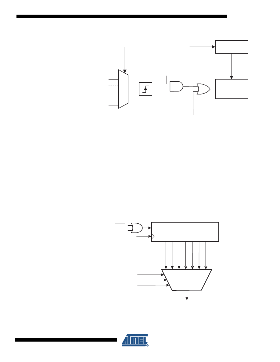
83
2535J–AVR–08/10
ATtiny13
Figure 14-2. ADC Auto Trigger Logic
Using the ADC Interrupt Flag as a trigger source makes the ADC start a new conversion as soon
as the ongoing conversion has finished. The ADC then operates in Free Running mode, con-
stantly sampling and updating the ADC Data Register. The first conversion must be started by
writing a logical one to the ADSC bit in ADCSRA. In this mode the ADC will perform successive
conversions independently of whether the ADC Interrupt Flag, ADIF is cleared or not.
If Auto Triggering is enabled, single conversions can be started by writing ADSC in ADCSRA to
one. ADSC can also be used to determine if a conversion is in progress. The ADSC bit will be
read as one during a conversion, independently of how the conversion was started.
14.5 Prescaling and Conversion Timing
By default, the successive approximation circuitry requires an input clock frequency between 50
kHz and 200 kHz to get maximum resolution. If a lower resolution than 10 bits is needed, the
input clock frequency to the ADC can be higher than 200 kHz to get a higher sample rate.
Figure 14-3. ADC Prescaler
The ADC module contains a prescaler, which generates an acceptable ADC clock frequency
from any CPU frequency above 100 kHz. The prescaling is set by the ADPS bits in ADCSRA.
ADSC
ADIF
SOURCE 1
SOURCE n
ADTS[2:0]
CONVERSION
LOGIC
PRESCALER
START
CLK
ADC
.
.
.
.
EDGE
DETECTOR
ADATE
7-BIT ADC PRESCALER
ADC CLOCK SOURCE
CK
ADPS0
ADPS1
ADPS2
CK/128
CK/2
CK/4
CK/8
CK/16
CK/32
CK/64
Reset
ADEN
START
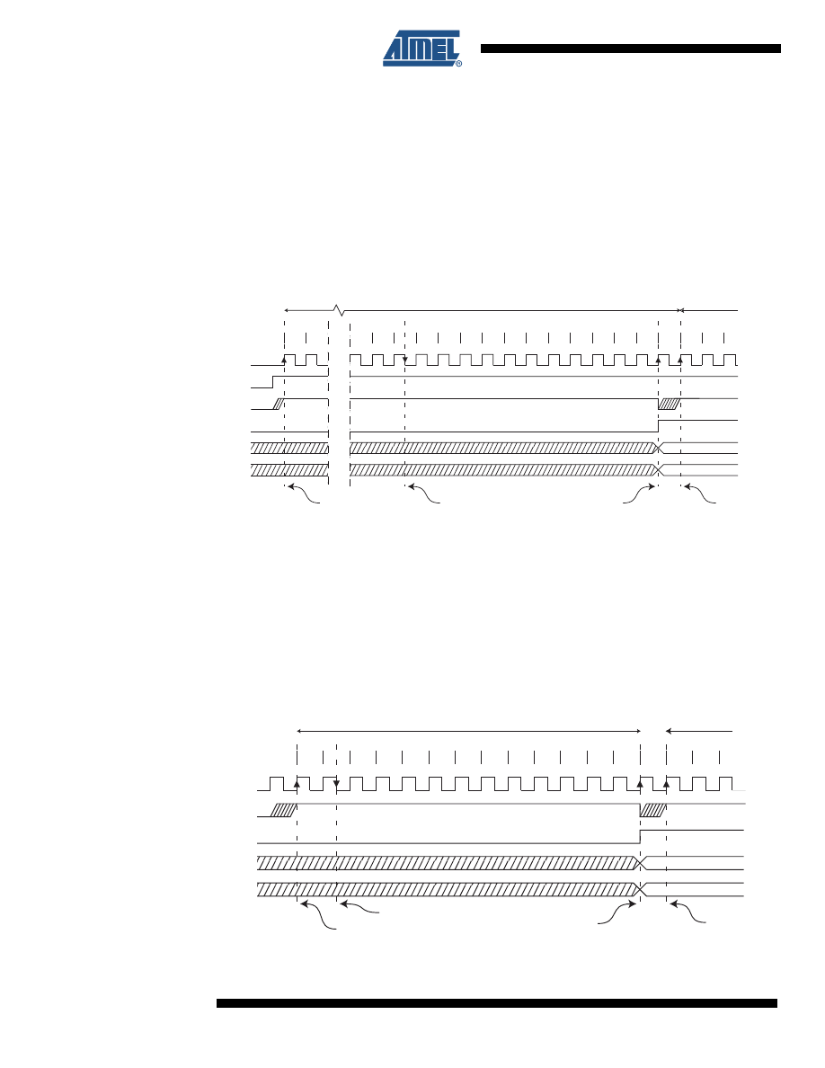
84
2535J–AVR–08/10
ATtiny13
The prescaler starts counting from the moment the ADC is switched on by setting the ADEN bit
in ADCSRA. The prescaler keeps running for as long as the ADEN bit is set, and is continuously
reset when ADEN is low.
When initiating a single ended conversion by setting the ADSC bit in ADCSRA, the conversion
starts at the following rising edge of the ADC clock cycle.
A normal conversion takes 13 ADC clock cycles. The first conversion after the ADC is switched
on (ADEN in ADCSRA is set) takes 25 ADC clock cycles in order to initialize the analog circuitry,
as shown in
Figure 14-4. ADC Timing Diagram, First Conversion (Single Conversion Mode)
When the bandgap reference voltage is used as input to the ADC, it will take a certain time for
the voltage to stabilize. If not stabilized, the first value read after the first conversion may be
wrong.
The actual sample-and-hold takes place 1.5 ADC clock cycles after the start of a normal conver-
sion and 14.5 ADC clock cycles after the start of an first conversion. When a conversion is
complete, the result is written to the ADC Data Registers, and ADIF is set. In Single Conversion
mode, ADSC is cleared simultaneously. The software may then set ADSC again, and a new
conversion will be initiated on the first rising ADC clock edge.
Figure 14-5. ADC Timing Diagram, Single Conversion
Sign and MSB of Result
LSB of Result
ADC Clock
ADSC
Sample & Hold
ADIF
ADCH
ADCL
Cycle Number
ADEN
1
2
12
13
14
15
16
17
18
19
20
21
22
23
24
25
1
2
First Conversion
Next
Conversion
3
MUX and REFS
Update
MUX and REFS
Update
Conversion
Complete
1
2
3
4
5
6
7
8
9
10
11
12
13
Sign and MSB of Result
LSB of Result
ADC Clock
ADSC
ADIF
ADCH
ADCL
Cycle Number
1
2
One Conversion
Next Conversion
3
Sample & Hold
MUX and REFS
Update
Conversion
Complete
MUX and REFS
Update
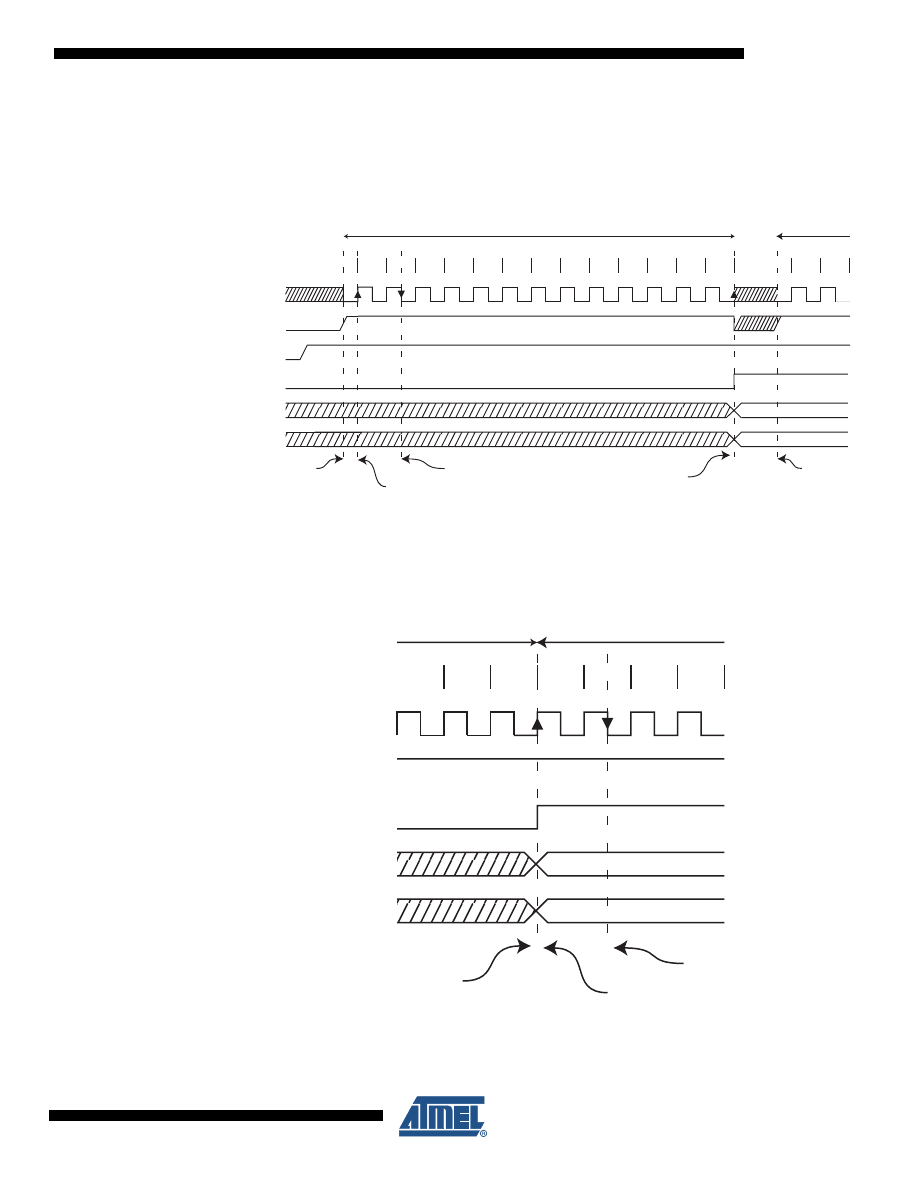
85
2535J–AVR–08/10
ATtiny13
When Auto Triggering is used, the prescaler is reset when the trigger event occurs, as shown in
below. This assures a fixed delay from the trigger event to the start of conversion. In
this mode, the sample-and-hold takes place two ADC clock cycles after the rising edge on the
trigger source signal. Three additional CPU clock cycles are used for synchronization logic.
Figure 14-6. ADC Timing Diagram, Auto Triggered Conversion
In Free Running mode, a new conversion will be started immediately after the conversion com-
pletes, while ADSC remains high.
Figure 14-7. ADC Timing Diagram, Free Running Conversion
1
2
3
4
5
6
7
8
9
10
11
12
13
Sign and MSB of Result
LSB of Result
ADC Clock
Trigger
Source
ADIF
ADCH
ADCL
Cycle Number
1
2
One Conversion
Next Conversion
Conversion
Complete
Prescaler
Reset
ADATE
Prescaler
Reset
Sample &
Hold
MUX and REFS
Update
11
12
13
Sign and MSB of Result
LSB of Result
ADC Clock
ADSC
ADIF
ADCH
ADCL
Cycle Number
1
2
One Conversion
Next Conversion
3
4
Conversion
Complete
Sample & Hold
MUX and REFS
Update

86
2535J–AVR–08/10
ATtiny13
For a summary of conversion times, see
14.6 Changing Channel or Reference Selection
The MUXn and REFS1:0 bits in the ADMUX Register are single buffered through a temporary
register to which the CPU has random access. This ensures that the channels and reference
selection only takes place at a safe point during the conversion. The channel and reference
selection is continuously updated until a conversion is started. Once the conversion starts, the
channel and reference selection is locked to ensure a sufficient sampling time for the ADC. Con-
tinuous updating resumes in the last ADC clock cycle before the conversion completes (ADIF in
ADCSRA is set). Note that the conversion starts on the following rising ADC clock edge after
ADSC is written. The user is thus advised not to write new channel or reference selection values
to ADMUX until one ADC clock cycle after ADSC is written.
If Auto Triggering is used, the exact time of the triggering event can be indeterministic. Special
care must be taken when updating the ADMUX Register, in order to control which conversion
will be affected by the new settings.
If both ADATE and ADEN is written to one, an interrupt event can occur at any time. If the
ADMUX Register is changed in this period, the user cannot tell if the next conversion is based
on the old or the new settings. ADMUX can be safely updated in the following ways:
• When ADATE or ADEN is cleared.
• During conversion, minimum one ADC clock cycle after the trigger event.
• After a conversion, before the Interrupt Flag used as trigger source is cleared.
When updating ADMUX in one of these conditions, the new settings will affect the next ADC
conversion.
14.6.1
ADC Input Channels
When changing channel selections, the user should observe the following guidelines to ensure
that the correct channel is selected:
In Single Conversion mode, always select the channel before starting the conversion. The chan-
nel selection may be changed one ADC clock cycle after writing one to ADSC. However, the
simplest method is to wait for the conversion to complete before changing the channel selection.
In Free Running mode, always select the channel before starting the first conversion. The chan-
nel selection may be changed one ADC clock cycle after writing one to ADSC. However, the
simplest method is to wait for the first conversion to complete, and then change the channel
selection. Since the next conversion has already started automatically, the next result will reflect
the previous channel selection. Subsequent conversions will reflect the new channel selection.
Table 14-1.
ADC Conversion Time
Condition
Sample & Hold (Cycles
from Start of Conversion)
Conversion Time (Cycles)
First conversion
13.5
25
Normal conversions
1.5
13
Auto Triggered conversions
2
13.5
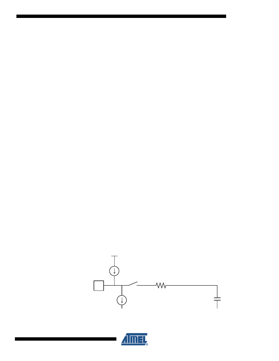
87
2535J–AVR–08/10
ATtiny13
14.6.2
ADC Voltage Reference
The reference voltage for the ADC (V
REF
) indicates the conversion range for the ADC. Single
ended channels that exceed V
REF
will result in codes close to 0x3FF. V
REF
can be selected as
either V
CC
, or internal 1.1V reference. The first ADC conversion result after switching reference
voltage source may be inaccurate, and the user is advised to discard this result.
14.7 ADC Noise Canceler
The ADC features a noise canceler that enables conversion during sleep mode to reduce noise
induced from the CPU core and other I/O peripherals. The noise canceler can be used with ADC
Noise Reduction and Idle mode. To make use of this feature, the following procedure should be
used:
• Make sure that the ADC is enabled and is not busy converting. Single Conversion mode must
be selected and the ADC conversion complete interrupt must be enabled.
• Enter ADC Noise Reduction mode (or Idle mode). The ADC will start a conversion once the
CPU has been halted.
• If no other interrupts occur before the ADC conversion completes, the ADC interrupt will
wake up the CPU and execute the ADC Conversion Complete interrupt routine. If another
interrupt wakes up the CPU before the ADC conversion is complete, the interrupt will be
executed, and an ADC Conversion Complete interrupt request will be generated when the
ADC conversion completes. The CPU will remain in active mode until a new sleep command
is executed.
Note that the ADC will not be automatically turned off when entering other sleep modes than Idle
mode and ADC Noise Reduction mode. The user is advised to write zero to ADEN before enter-
ing such sleep modes to avoid excessive power consumption.
14.8 Analog Input Circuitry
The analog input circuitry for single ended channels is shown in
An analog source
applied to ADCn is subjected to pin capacitance and input leakage of that pin, regardless if the
channel is chosen as input for the ADC, or not. When the channel is selected, the source drives
the S/H capacitor through the series resistance (combined resistance in input path).
Figure 14-8. Analog Input Circuitry
Note:
The capacitor in the figure depicts the total capacitance, including the sample/hold capacitor and
any stray or parasitic capacitance inside the device. The value given is worst case.
n
I
IH
1..100 k
ohm
C
S/H
= 14 pF
I
IL

88
2535J–AVR–08/10
ATtiny13
The ADC is optimized for analog signals with an output impedance of approximately 10 k
Ω or
less. If such a source is used, the sampling time will be negligible. If a source with higher imped-
ance is used, the sampling time will depend on how long time the source needs to charge the
S/H capacitor, with can vary widely. The user is recommended to only use low impedant sources
with slowly varying signals, since this minimizes the required charge transfer to the S/H
capacitor.
Signal components higher than the Nyquist frequency (f
ADC
/2) should not be present to avoid
distortion from unpredictable signal convolution. The user is advised to remove high frequency
components with a low-pass filter before applying the signals as inputs to the ADC.
14.9 Analog Noise Canceling Techniques
Digital circuitry inside and outside the device generates EMI which might affect the accuracy of
analog measurements. When conversion accuracy is critical, the noise level can be reduced by
applying the following techniques:
• Keep analog signal paths as short as possible.
• Make sure analog tracks run over the analog ground plane.
• Keep analog tracks well away from high-speed switching digital tracks.
• If any port pin is used as a digital output, it mustn’t switch while a conversion is in progress.
• Place bypass capacitors as close to V
CC
and GND pins as possible.
Where high ADC accuracy is required it is recommended to use ADC Noise Reduction Mode, as
described in
. This is especially the case when system clock frequency
is above 1 MHz. A good system design with properly placed, external bypass capacitors does
reduce the need for using ADC Noise Reduction Mode
14.10 ADC Accuracy Definitions
An n-bit single-ended ADC converts a voltage linearly between GND and V
REF
in 2
n
steps
(LSBs). The lowest code is read as 0, and the highest code is read as 2
n
-1.
Several parameters describe the deviation from the ideal behavior:
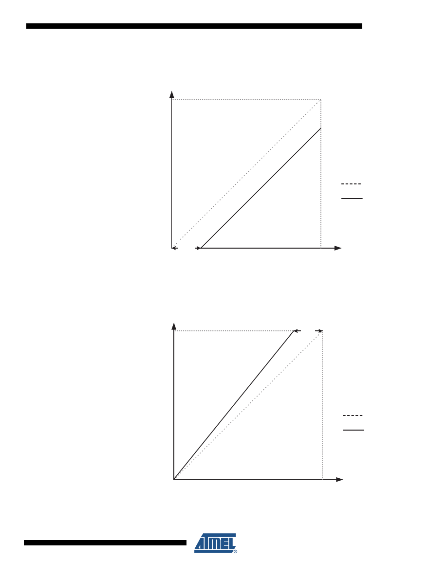
89
2535J–AVR–08/10
ATtiny13
• Offset: The deviation of the first transition (0x000 to 0x001) compared to the ideal transition
(at 0.5 LSB). Ideal value: 0 LSB.
Figure 14-9. Offset Error
• Gain Error: After adjusting for offset, the Gain Error is found as the deviation of the last
transition (0x3FE to 0x3FF) compared to the ideal transition (at 1.5 LSB below maximum).
Ideal value: 0 LSB
Figure 14-10. Gain Error
Output Code
V
REF
Input Voltage
Ideal ADC
Actual ADC
Offset
Error
Output Code
V
REF
Input Voltage
Ideal ADC
Actual ADC
Gain
Error
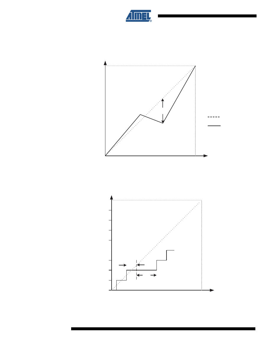
90
2535J–AVR–08/10
ATtiny13
• Integral Non-linearity (INL): After adjusting for offset and gain error, the INL is the maximum
deviation of an actual transition compared to an ideal transition for any code. Ideal value: 0
LSB.
Figure 14-11. Integral Non-linearity (INL)
• Differential Non-linearity (DNL): The maximum deviation of the actual code width (the interval
between two adjacent transitions) from the ideal code width (1 LSB). Ideal value: 0 LSB.
Figure 14-12. Differential Non-linearity (DNL)
Output Code
V
REF
Input Voltage
Ideal ADC
Actual ADC
INL
Output Code
0x3FF
0x000
0
V
REF
Input Voltage
DNL
1 LSB

91
2535J–AVR–08/10
ATtiny13
• Quantization Error: Due to the quantization of the input voltage into a finite number of codes,
a range of input voltages (1 LSB wide) will code to the same value. Always ± 0.5 LSB.
• Absolute Accuracy: The maximum deviation of an actual (unadjusted) transition compared to
an ideal transition for any code. This is the compound effect of offset, gain error, differential
error, non-linearity, and quantization error. Ideal value: ± 0.5 LSB.
14.11 ADC Conversion Result
After the conversion is complete (ADIF is high), the conversion result can be found in the ADC
Result Registers (ADCL, ADCH).
For single ended conversion, the result is
where V
IN
is the voltage on the selected input pin and V
REF
the selected voltage reference (see
and
). 0x000 represents analog ground, and
0x3FF represents the selected reference voltage minus one LSB.
14.12 Register Description
14.12.1
ADMUX – ADC Multiplexer Selection Register
• Bit 7 – Res: Reserved Bit
This bit is reserved bit in the ATtiny13 and will always read as zero.
• Bit 6 – REFS0: Reference Selection Bit
This bit selects the voltage reference for the ADC, as shown in
. If this bit is changed
during a conversion, the change will not go in effect until this conversion is complete (ADIF in
ADCSRA is set).
•
Bit 5 – ADLAR: ADC Left Adjust Result
The ADLAR bit affects the presentation of the ADC conversion result in the ADC Data Register.
Write one to ADLAR to left adjust the result. Otherwise, the result is right adjusted. Changing the
ADLAR bit will affect the ADC Data Register immediately, regardless of any ongoing conver-
sions. For a complete description of this bit, see
“ADCL and ADCH – The ADC Data Register” on
ADC
V
IN
1024
⋅
V
REF
--------------------------
=
Bit
7
6
5
4
3
2
1
0
–
REFS0
ADLAR
–
–
–
MUX1
MUX0
ADMUX
Read/Write
R
R/W
R/W
R
R
R
R/W
R/W
Initial Value
0
0
0
0
0
0
0
0
Table 14-2.
Voltage Reference Selections for ADC
REFS0
Voltage Reference Selection
0
V
CC
used as analog reference.
1
Internal Voltage Reference.

92
2535J–AVR–08/10
ATtiny13
• Bits 4:2 – Res: Reserved Bits
These bits are reserved bits in the ATtiny13 and will always read as zero.
• Bits 1:0 – MUX1:0: Analog Channel Selection Bits
The value of these bits selects which combination of analog inputs are connected to the ADC.
See
for details.
If these bits are changed during a conversion, the change
will not go in effect until this conversion is complete (ADIF in ADCSRA is set).
14.12.2
ADCSRA – ADC Control and Status Register A
• Bit 7 – ADEN: ADC Enable
Writing this bit to one enables the ADC. By writing it to zero, the ADC is turned off. Turning the
ADC off while a conversion is in progress, will terminate this conversion.
• Bit 6 – ADSC: ADC Start Conversion
In Single Conversion mode, write this bit to one to start each conversion. In Free Running mode,
write this bit to one to start the first conversion. The first conversion after ADSC has been written
after the ADC has been enabled, or if ADSC is written at the same time as the ADC is enabled,
will take 25 ADC clock cycles instead of the normal 13. This first conversion performs initializa-
tion of the ADC.
ADSC will read as one as long as a conversion is in progress. When the conversion is complete,
it returns to zero. Writing zero to this bit has no effect.
• Bit 5 – ADATE: ADC Auto Trigger Enable
When this bit is written to one, Auto Triggering of the ADC is enabled. The ADC will start a con-
version on a positive edge of the selected trigger signal. The trigger source is selected by setting
the ADC Trigger Select bits, ADTS in ADCSRB.
• Bit 4 – ADIF: ADC Interrupt Flag
This bit is set when an ADC conversion completes and the data registers are updated. The ADC
Conversion Complete Interrupt is executed if the ADIE bit and the I-bit in SREG are set. ADIF is
cleared by hardware when executing the corresponding interrupt handling vector. Alternatively,
ADIF is cleared by writing a logical one to the flag. Beware that if doing a Read-Modify-Write on
ADCSRA, a pending interrupt can be disabled. This also applies if the SBI and CBI instructions
are used.
Table 14-3.
Input Channel Selections
MUX1..0
Single Ended Input
00
ADC0 (PB5)
01
ADC1 (PB2)
10
ADC2 (PB4)
11
ADC3 (PB3)
Bit
7
6
5
4
3
2
1
0
ADEN
ADSC
ADATE
ADIF
ADIE
ADPS2
ADPS1
ADPS0
ADCSRA
Read/Write
R/W
R/W
R/W
R/W
R/W
R/W
R/W
R/W
Initial Value
0
0
0
0
0
0
0
0
93
2535J–AVR–08/10
ATtiny13
• Bit 3 – ADIE: ADC Interrupt Enable
When this bit is written to one and the I-bit in SREG is set, the ADC Conversion Complete Inter-
rupt is activated.
• Bits 2:0 – ADPS2:0: ADC Prescaler Select Bits
These bits determine the division factor between the system clock frequency and the input clock
to the ADC.
14.12.3
ADCL and ADCH – The ADC Data Register
14.12.3.1
ADLAR = 0
14.12.3.2
ADLAR = 1
When an ADC conversion is complete, the result is found in these two registers.
When ADCL is read, the ADC Data Register is not updated until ADCH is read. Consequently, if
the result is left adjusted and no more than 8-bit precision is required, it is sufficient to read
ADCH. Otherwise, ADCL must be read first, then ADCH.
Table 14-4.
ADC Prescaler Selections
ADPS2
ADPS1
ADPS0
Division Factor
0
0
0
2
0
0
1
2
0
1
0
4
0
1
1
8
1
0
0
16
1
0
1
32
1
1
0
64
1
1
1
128
Bit
15
14
13
12
11
10
9
8
–
–
–
–
–
–
ADC9
ADC8
ADCH
ADC7
ADC6
ADC5
ADC4
ADC3
ADC2
ADC1
ADC0
ADCL
7
6
5
4
3
2
1
0
Read/Write
R
R
R
R
R
R
R
R
R
R
R
R
R
R
R
R
Initial Value
0
0
0
0
0
0
0
0
0
0
0
0
0
0
0
0
Bit
15
14
13
12
11
10
9
8
ADC9
ADC8
ADC7
ADC6
ADC5
ADC4
ADC3
ADC2
ADCH
ADC1
ADC0
–
–
–
–
–
–
ADCL
7
6
5
4
3
2
1
0
Read/Write
R
R
R
R
R
R
R
R
R
R
R
R
R
R
R
R
Initial Value
0
0
0
0
0
0
0
0
0
0
0
0
0
0
0
0
94
2535J–AVR–08/10
ATtiny13
The ADLAR bit in ADMUX, and the MUXn bits in ADMUX affect the way the result is read from
the registers. If ADLAR is set, the result is left adjusted. If ADLAR is cleared (default), the result
is right adjusted.
• ADC9:0: ADC Conversion Result
These bits represent the result from the conversion, as detailed in
14.12.4
ADCSRB – ADC Control and Status Register B
• Bits 7, 5:3 – Res: Reserved Bits
These bits are reserved bits in the ATtiny13 and will always read as zero.
• Bits 2:0 – ADTS2:0: ADC Auto Trigger Source
If ADATE in ADCSRA is written to one, the value of these bits selects which source will trigger
an ADC conversion. If ADATE is cleared, the ADTS2:0 settings will have no effect. A conversion
will be triggered by the rising edge of the selected Interrupt Flag. Note that switching from a trig-
ger source that is cleared to a trigger source that is set, will generate a positive edge on the
trigger signal. If ADEN in ADCSRA is set, this will start a conversion. Switching to Free Running
mode (ADTS[2:0]=0) will not cause a trigger event, even if the ADC Interrupt Flag is set
.
14.12.5
DIDR0 – Digital Input Disable Register 0
• Bits 5:2 – ADC3D:ADC0D: ADC3:0 Digital Input Disable
When a bit is written logic one, the digital input buffer on the corresponding ADC pin is disabled.
The corresponding PIN register bit will always read as zero when this bit is set. When an analog
signal is applied to the ADC7..0 pin and the digital input from this pin is not needed, this bit
should be written logic one to reduce power consumption in the digital input buffer.
Bit
7
6
5
4
3
2
1
0
–
ACME
–
–
–
ADTS2
ADTS1
ADTS0
ADCSRB
Read/Write
R
R/W
R
R
R
R/W
R/W
R/W
Initial Value
0
0
0
0
0
0
0
0
Table 14-5.
ADC Auto Trigger Source Selections
ADTS2
ADTS1
ADTS0
Trigger Source
0
0
0
Free Running mode
0
0
1
Analog Comparator
0
1
0
External Interrupt Request 0
0
1
1
Timer/Counter Compare Match A
1
0
0
Timer/Counter Overflow
1
0
1
Timer/Counter Compare Match B
1
1
0
Pin Change Interrupt Request
Bit
7
6
5
4
3
2
1
0
–
–
ADC0D
ADC2D
ADC3D
ADC1D
AIN1D
AIN0D
DIDR0
Read/Write
R
R
R/W
R/W
R/W
R/W
R/W
R/W
Initial Value
0
0
0
0
0
0
0
0
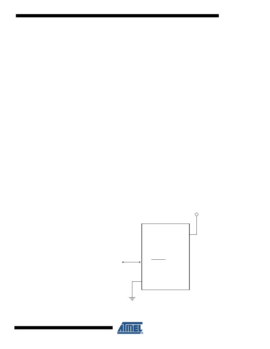
95
2535J–AVR–08/10
ATtiny13
15. debugWIRE On-chip Debug System
15.1 Features
•
Complete Program Flow Control
•
Emulates All On-chip Functions, Both Digital and Analog, except RESET Pin
•
Real-time Operation
•
Symbolic Debugging Support (Both at C and Assembler Source Level, or for Other HLLs)
•
Unlimited Number of Program Break Points (Using Software Break Points)
•
Non-intrusive Operation
•
Electrical Characteristics Identical to Real Device
•
Automatic Configuration System
•
High-Speed Operation
•
Programming of Non-volatile Memories
15.2 Overview
The debugWIRE On-chip debug system uses a One-wire, bi-directional interface to control the
program flow, execute AVR instructions in the CPU and to program the different non-volatile
memories.
15.3 Physical Interface
When the debugWIRE Enable (DWEN) fuse is programmed and lock bits are unprogrammed,
the debugWIRE system within the target device is activated. The RESET port pin is configured
as a wire-AND (open-drain) bi-directional I/O pin with pull-up enabled and becomes the commu-
nication gateway between target and emulator.
shows the schematic of a target MCU, with debugWIRE enabled, and the emulator
connector. The system clock is not affected by debugWIRE and will always be the clock source
selected by the CKSEL fuses.
Figure 15-1. The debugWIRE Setup
dW
GND
dW(RESET)
VCC
1.8 - 5.5V

96
2535J–AVR–08/10
ATtiny13
When designing a system where debugWIRE will be used, the following must be observed:
• Pull-Up resistor on the dW/(RESET) line must be in the range of 10k to 20 k
Ω. However, the
pull-up resistor is optional.
• Connecting the RESET pin directly to V
CC
will not work.
• Capacitors inserted on the RESET pin must be disconnected when using debugWire.
• All external reset sources must be disconnected.
15.4 Software Break Points
debugWIRE supports Program memory Break Points by the AVR Break instruction. Setting a
Break Point in AVR Studio
®
will insert a BREAK instruction in the Program memory. The instruc-
tion replaced by the BREAK instruction will be stored. When program execution is continued, the
stored instruction will be executed before continuing from the Program memory. A break can be
inserted manually by putting the BREAK instruction in the program.
The Flash must be re-programmed each time a Break Point is changed. This is automatically
handled by AVR Studio through the debugWIRE interface. The use of Break Points will therefore
reduce the Flash Data retention. Devices used for debugging purposes should not be shipped to
end customers.
15.5 Limitations of debugWIRE
The debugWIRE communication pin (dW) is physically located on the same pin as External
Reset (RESET). An External Reset source is therefore not supported when the debugWIRE is
enabled.
The debugWIRE system accurately emulates all I/O functions when running at full speed, i.e.,
when the program in the CPU is running. When the CPU is stopped, care must be taken while
accessing some of the I/O Registers via the debugger (AVR Studio). See the debugWIRE docu-
mentation for detailed description of the limitations.
The debugWIRE interface is asynchronous, which means that the debugger needs to synchro-
nize to the system clock. If the system clock is changed by software (e.g. by writing CLKPS bits)
communication via debugWIRE may fail. Also, clock frequencies below 100 kHz may cause
communication problems.
A programmed DWEN fuse enables some parts of the clock system to be running in all sleep
modes. This will increase the power consumption while in sleep. Thus, the DWEN fuse should
be disabled when debugWire is not used.
15.6 Register Description
The following section describes the registers used with the debugWire.
15.6.1
DWDR –debugWire Data Register
The DWDR Register provides a communication channel from the running program in the MCU
to the debugger. This register is only accessible by the debugWIRE and can therefore not be
used as a general purpose register in the normal operations.
Bit
7
6
5
4
3
2
1
0
DWDR[7:0]
DWDR
Read/Write
R/W
R/W
R/W
R/W
R/W
R/W
R/W
R/W
Initial Value
0
0
0
0
0
0
0
0

97
2535J–AVR–08/10
ATtiny13
16. Self-Programming the Flash
The device provides a Self-Programming mechanism for downloading and uploading program
code by the MCU itself. The Self-Programming can use any available data interface and associ-
ated protocol to read code and write (program) that code into the Program memory. The SPM
instruction is disabled by default but it can be enabled by programming the SELFPRGEN fuse
(to “0”).
The Program memory is updated in a page by page fashion. Before programming a page with
the data stored in the temporary page buffer, the page must be erased. The temporary page buf-
fer is filled one word at a time using SPM and the buffer can be filled either before the Page
Erase command or between a Page Erase and a Page Write operation:
Alternative 1, fill the buffer before a Page Erase
• Fill temporary page buffer
• Perform a Page Erase
• Perform a Page Write
Alternative 2, fill the buffer after Page Erase
• Perform a Page Erase
• Fill temporary page buffer
• Perform a Page Write
If only a part of the page needs to be changed, the rest of the page must be stored (for example
in the temporary page buffer) before the erase, and then be re-written. When using alternative 1,
the Boot Loader provides an effective Read-Modify-Write feature which allows the user software
to first read the page, do the necessary changes, and then write back the modified data. If alter-
native 2 is used, it is not possible to read the old data while loading since the page is already
erased. The temporary page buffer can be accessed in a random sequence. It is essential that
the page address used in both the Page Erase and Page Write operation is addressing the
same page.
16.1 Performing Page Erase by SPM
To execute Page Erase, set up the address in the Z-pointer, write “00000011” to SPMCSR and
execute SPM within four clock cycles after writing SPMCSR. The data in R1 and R0 is ignored.
The page address must be written to PCPAGE in the Z-register. Other bits in the Z-pointer will
be ignored during this operation.
Note:
The CPU is halted during the Page Erase operation.
16.2 Filling the Temporary Buffer (Page Loading)
To write an instruction word, set up the address in the Z-pointer and data in R1:R0, write
“00000001” to SPMCSR and execute SPM within four clock cycles after writing SPMCSR. The
content of PCWORD in the Z-register is used to address the data in the temporary buffer. The
temporary buffer will auto-erase after a Page Write operation or by writing the CTPB bit in
SPMCSR. It is also erased after a system reset. Note that it is not possible to write more than
one time to each address without erasing the temporary buffer.
98
2535J–AVR–08/10
ATtiny13
If the EEPROM is written in the middle of an SPM Page Load operation, all data loaded will be
lost.
16.3 Performing a Page Write
To execute Page Write, set up the address in the Z-pointer, write “00000101” to SPMCSR and
execute SPM within four clock cycles after writing SPMCSR. The data in R1 and R0 is ignored.
The page address must be written to PCPAGE. Other bits in the Z-pointer must be written to
zero during this operation.
Note:
The CPU is halted during the Page Write operation.
16.4 Addressing the Flash During Self-Programming
The Z-pointer is used to address the SPM commands.
Since the Flash is organized in pages (see
), the Program Counter can
be treated as having two different sections. One section, consisting of the least significant bits, is
addressing the words within a page, while the most significant bits are addressing the pages.
This is shown in
. Note that the Page Erase and Page Write operations are
addressed independently. Therefore it is of major importance that the software addresses the
same page in both the Page Erase and Page Write operation.
Figure 16-1. Addressing the Flash During SPM
Note:
1. The variables used in
.
Bit
15
14
13
12
11
10
9
8
ZH (R31)
Z15
Z14
Z13
Z12
Z11
Z10
Z9
Z8
ZL (R30)
Z7
Z6
Z5
Z4
Z3
Z2
Z1
Z0
7
6
5
4
3
2
1
0
PROGRAM MEMORY
0
1
15
Z - REGISTER
BIT
0
ZPAGEMSB
WORD ADDRESS
WITHIN A PAGE
PAGE ADDRESS
WITHIN THE FLASH
ZPCMSB
INSTRUCTION WORD
PAGE
PCWORD[PAGEMSB:0]:
00
01
02
PAGEEND
PAGE
PCWORD
PCPAGE
PCMSB
PAGEMSB
PROGRAM
COUNTER

99
2535J–AVR–08/10
ATtiny13
The LPM instruction uses the Z-pointer to store the address. Since this instruction addresses the
Flash byte-by-byte, also the LSB (bit Z0) of the Z-pointer is used.
16.5 EEPROM Write Prevents Writing to SPMCSR
Note that an EEPROM write operation will block all software programming to Flash. Reading the
fuses and lock bits from software will also be prevented during the EEPROM write operation. It is
recommended that the user checks the status bit (EEPE) in the EECR Register and verifies that
the bit is cleared before writing to the SPMCSR Register.
16.6 Reading Fuse and Lock Bits from Firmware
It is possible to read fuse and lock bits from software.
16.6.1
Reading Lock Bits from Firmware
Issuing an LPM instruction within three CPU cycles after RFLB and SELFPRGEN bits have
been set in SPMCSR will return lock bit values in the destination register. The RFLB and SELF-
PRGEN bits automatically clear upon completion of reading the lock bits, or if no LPM instruction
is executed within three CPU cycles, or if no SPM instruction is executed within four CPU cycles.
When RFLB and SELFPRGEN are cleared, LPM functions normally.
To read the lock bits, follow the below procedure.
1. Load the Z-pointer with 0x0001.
2. Set RFLB and SELFPRGEN bits in SPMCSR.
3. Issuing an LPM instruction within three clock cycles will return lock bits in the destina-
tion register.
If successful, the contents of the destination register are as follows.
“Program And Data Memory Lock Bits” on page 102
for more information on lock
bits.
16.6.2
Reading Fuse Bits from Firmware
The algorithm for reading fuse bytes is similar to the one described above for reading lock bits,
only the addresses are different.
To read the Fuse Low Byte (FLB), follow the below procedure:
1. Load the Z-pointer with 0x0000.
2. Set RFLB and SELFPRGEN bits in SPMCSR.
3. Issuing an LPM instruction within three clock cycles will FLB in the destination register.
If successful, the contents of the destination register are as follows.
Bit
7
6
5
4
3
2
1
0
Rd
–
–
–
–
–
–
LB2
LB1
Bit
7
6
5
4
3
2
1
0
Rd
FLB7
FLB6
FLB5
FLB4
FLB3
FLB2
FLB1
FLB0

100
2535J–AVR–08/10
ATtiny13
To read the Fuse High Byte (FHB), simply replace the address in the Z-pointer with 0x0003 and
repeat the procedure above.
If successful, the contents of the destination register are as follows.
See sections
“Program And Data Memory Lock Bits” on page 102
for more information on fuse and lock bits.
16.7 Preventing Flash Corruption
During periods of low V
CC
, the Flash program can be corrupted because the supply voltage is
too low for the CPU and the Flash to operate properly. These issues are the same as for board
level systems using the Flash, and the same design solutions should be applied.
A Flash program corruption can be caused by two situations when the voltage is too low. First, a
regular write sequence to the Flash requires a minimum voltage to operate correctly. Secondly,
the CPU itself can execute instructions incorrectly, if the supply voltage for executing instructions
is too low.
Flash corruption can easily be avoided by following these design recommendations (one is
sufficient):
1. Keep the AVR RESET active (low) during periods of insufficient power supply voltage.
This can be done by enabling the internal Brown-out Detector (BOD) if the operating
voltage matches the detection level. If not, an external low V
CC
reset protection circuit
can be used. If a reset occurs while a write operation is in progress, the write operation
will be completed provided that the power supply voltage is sufficient.
2. Keep the AVR core in Power-down sleep mode during periods of low V
CC
. This will pre-
vent the CPU from attempting to decode and execute instructions, effectively protecting
the SPMCSR Register and thus the Flash from unintentional writes.
16.8 Programming Time for Flash when Using SPM
The calibrated RC Oscillator is used to time Flash accesses.
shows the
typical programming time for Flash accesses from the CPU.
Note:
1. The min and max programming times is per individual operation.
Bit
7
6
5
4
3
2
1
0
Rd
FHB7
FHB6
FHB5
FHB4
FHB3
FHB2
FHB1
FHB0
Table 16-1.
SPM Programming Time
Symbol
Min Programming Time
Max Programming Time
Flash write (Page Erase, Page Write, and
write lock bits by SPM)
3.7 ms
4.5 ms

101
2535J–AVR–08/10
ATtiny13
16.9 Register Description
16.9.1
SPMCSR – Store Program Memory Control and Status Register
The Store Program Memory Control and Status Register contains the control bits needed to con-
trol the Program memory operations.
• Bits 7..5 – Res: Reserved Bits
These bits are reserved bits in the ATtiny13 and always read as zero.
• Bit 4 – CTPB: Clear Temporary Page Buffer
If the CTPB bit is written while filling the temporary page buffer, the temporary page buffer will be
cleared and the data will be lost.
• Bit 3 – RFLB: Read Fuse and Lock Bits
An LPM instruction within three cycles after RFLB and SELFPRGEN are set in the SPMCSR
Register, will read either the lock bits or the fuse bits (depending on Z0 in the Z-pointer) into the
destination register. See
“EEPROM Write Prevents Writing to SPMCSR” on page 99
for details.
• Bit 2 – PGWRT: Page Write
If this bit is written to one at the same time as SELFPRGEN, the next SPM instruction within four
clock cycles executes Page Write, with the data stored in the temporary buffer. The page
address is taken from the high part of the Z-pointer. The data in R1 and R0 are ignored. The
PGWRT bit will auto-clear upon completion of a Page Write, or if no SPM instruction is executed
within four clock cycles. The CPU is halted during the entire Page Write operation.
• Bit 1 – PGERS: Page Erase
If this bit is written to one at the same time as SELFPRGEN, the next SPM instruction within four
clock cycles executes Page Erase. The page address is taken from the high part of the Z-
pointer. The data in R1 and R0 are ignored. The PGERS bit will auto-clear upon completion of a
Page Erase, or if no SPM instruction is executed within four clock cycles. The CPU is halted dur-
ing the entire Page Write operation.
• Bit 0 – SELFPRGEN: Self Programming Enable
This bit enables the SPM instruction for the next four clock cycles. If written to one together with
either CTPB, RFLB, PGWRT, or PGERS, the following SPM instruction will have a special
meaning, see description above. If only SELFPRGEN is written, the following SPM instruction
will store the value in R1:R0 in the temporary page buffer addressed by the Z-pointer. The LSB
of the Z-pointer is ignored. The SELFPRGEN bit will auto-clear upon completion of an SPM
instruction, or if no SPM instruction is executed within four clock cycles. During Page Erase and
Page Write, the SELFPRGEN bit remains high until the operation is completed.
Writing any other combination than “10001”, “01001”, “00101”, “00011” or “00001” in the lower
five bits will have no effect.
Bit
7
6
5
4
3
2
1
0
–
–
–
CTPB
RFLB
PGWRT
PGERS
SELFPRGEN
SPMCSR
Read/Write
R
R
R
R/W
R/W
R/W
R/W
R/W
Initial Value
0
0
0
0
0
0
0
0

102
2535J–AVR–08/10
ATtiny13
17. Memory Programming
This section describes how ATtiny13 memories can be programmed.
17.1 Program And Data Memory Lock Bits
ATtiny13 provides two lock bits which can be left unprogrammed (“1”) or can be programmed
(“0”) to obtain the additional security listed in
. The lock bits can be
erased to “1” with the Chip Erase command, only.
Program memory can be read out via the debugWIRE interface when the DWEN fuse is pro-
grammed, even if the lock bits are set. Thus, when lock bit security is required, debugWIRE
should always be disabled by clearing the DWEN fuse.
Note:
1. “1” means unprogrammed, “0” means programmed
Notes: 1. Program fuse bits before lock bits. See section
2. “1” means unprogrammed, “0” means programmed
Table 17-1.
Lock Bit Byte
Lock Bit Byte
Bit No
Description
7
–
1 (unprogrammed)
6
–
1 (unprogrammed)
5
–
1 (unprogrammed)
4
–
1 (unprogrammed)
3
–
1 (unprogrammed)
2
–
1 (unprogrammed)
LB2
1
Lock bit
1 (unprogrammed)
LB1
0
Lock bit
1 (unprogrammed)
Table 17-2.
Lock Bit Protection Modes
Protection Type
LB Mode
LB2
LB1
1
1
1
No memory lock features enabled.
2
1
0
Further programming of the Flash and EEPROM is disabled in
High-voltage and Serial Programming mode. Fuse bits are
locked in both Serial and High-voltage Programming mode.
debugWire is disabled.
3
0
0
Further programming and verification of the Flash and
EEPROM is disabled in High-voltage and Serial Programming
mode. Fuse bits are locked in both Serial and High-voltage
Programming mode. debugWire is disabled.

103
2535J–AVR–08/10
ATtiny13
17.2 Fuse Bytes
The ATtiny13 has two fuse bytes.
and
describe
briefly the functionality of all the fuses and how they are mapped into the fuse bytes. Note that
the fuses are read as logical zero, “0”, if they are programmed.
Notes: 1. Enables SPM instruction. See
“Self-Programming the Flash” on page 97
.
2. DWEN must be unprogrammed when lock Bit security is required.
Memory Lock Bits” on page 102.
3. See
for BODLEVEL fuse decoding.
4. See
“Alternate Functions of Port B” on page 54
for description of RSTDISBL and DWEN fuses.
When programming the RSTDISBL fuse, High-voltage Serial programming has to be used to
change fuses to perform further programming.
Notes: 1. The SPIEN fuse is not accessible in SPI Programming mode.
2. Programming this fues will disable the Watchdog Timer Interrupt. See
for details.
3. See
“System Clock Prescaler” on page 26
for details.
4. The default value of SUT1..0 results in maximum start-up time for the default clock source.
See
for details.
5. The default setting of CKSEL1..0 results in internal RC Oscillator @ 9.6 MHz. See
for details.
Table 17-3.
Fuse High Byte
Fuse Bit
Bit No
Description
Default Value
–
7
–
1 (unprogrammed)
–
6
–
1 (unprogrammed)
–
5
–
1 (unprogrammed)
4
Self Programming Enable
1 (unprogrammed)
DWEN
3
debugWire Enable
1 (unprogrammed)
2
Brown-out Detector trigger level
1 (unprogrammed)
1
Brown-out Detector trigger level
1 (unprogrammed)
0
External Reset disable
1 (unprogrammed)
Table 17-4.
Fuse Low Byte
Fuse Bit
Bit No
Description
Default Value
SPIEN
7
Enable Serial Programming and Data
Downloading
0 (programmed)
(SPI prog. enabled)
EESAVE
6
Preserve EEPROM memory through
Chip Erase
1 (unprogrammed)
(memory not preserved)
WDTON
5
Watchdog Timer always on
1 (unprogrammed)
4
Divide clock by 8
0 (programmed)
3
Select start-up time
1 (unprogrammed)
2
Select start-up time
0 (programmed)
1
Select Clock source
1 (unprogrammed)
0
Select Clock source
0 (programmed)

104
2535J–AVR–08/10
ATtiny13
Note that fuse bits are locked if Lock Bit 1 (LB1) is programmed. Program the fuse bits before
programming the lock bits. The status of the fuse bits is not affected by Chip Erase.
Fuse bits can also be read by the device firmware. See section
.
17.2.1
Latching of Fuses
The fuse values are latched when the device enters programming mode and changes of the
fuse values will have no effect until the part leaves Programming mode. This does not apply to
the EESAVE fuse which will take effect once it is programmed. The fuses are also latched on
Power-up in Normal mode.
17.3 Calibration Bytes
The signature area of the ATtiny13 contains two bytes of calibration data for the internal oscilla-
tor. The calibration data in the high byte of address 0x00 is for use with the oscillator set to 9.6
MHz operation. During reset, this byte is automatically written into the OSCCAL register to
ensure correct frequency of the oscillator.
There is a separate calibration byte for the internal oscillator in 4.8 MHz mode of operation but
this data is not loaded automatically. The hardware always loads the 9.6 MHz calibraiton data
during reset. To use separate calibration data for the oscillator in 4.8 MHz mode the OSCCAL
register must be updated by firmware. The calibration data for 4.8 MHz operation is located in
the high byte at address 0x01 of the signature area.
17.4 Signature Bytes
All Atmel microcontrollers have a three-byte signature code which identifies the device. This
code can be read in both serial and high-voltage programming mode, even when the device is
locked. The three bytes reside in a separate address space.
For the ATtiny13 the signature bytes are:
• 0x000: 0x1E (indicates manufactured by Atmel).
• 0x001: 0x90 (indicates 1 KB Flash memory).
• 0x002: 0x07 (indicates ATtiny13 device when 0x001 is 0x90).
17.5 Page Size
Table 17-5.
No. of Words in a Page and No. of Pages in the Flash
Flash Size
Page Size
PCWORD
No. of Pages
PCPAGE
PCMSB
512 words (1K byte)
16 words
PC[3:0]
32
PC[8:4]
8
Table 17-6.
No. of Words in a Page and No. of Pages in the EEPROM
EEPROM Size
Page Size
PCWORD
No. of Pages
PCPAGE
EEAMSB
64 bytes
4 bytes
EEA[1:0]
16
EEA[5:2]
5
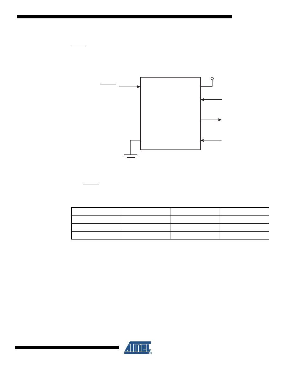
105
2535J–AVR–08/10
ATtiny13
17.6 Serial Programming
Both the Flash and EEPROM memory arrays can be programmed using the serial SPI bus while
RESET is pulled to GND. The serial interface consists of pins SCK, MOSI (input) and MISO (out-
put). See
.
Figure 17-1. Serial Programming and Verify
Note:
If clocked by internal oscillator there is no need to connect a clock source to the CLKI pin.
After RESET is set low, the Programming Enable instruction needs to be executed first before
program/erase operations can be executed.
Note:
In
above, the pin mapping for SPI programming is listed. Not all parts use the SPI pins
dedicated for the internal SPI interface.
When programming the EEPROM, an auto-erase cycle is built into the self-timed programming
operation (in the Serial mode ONLY) and there is no need to first execute the Chip Erase
instruction. The Chip Erase operation turns the content of every memory location in both the
Program and EEPROM arrays into 0xFF.
Depending on CKSEL fuses, a valid clock must be present. The minimum low and high periods
for the serial clock (SCK) input are defined as follows:
Low: > 2 CPU clock cycles for f
ck
< 12 MHz, 3 CPU clock cycles for f
ck
>= 12 MHz
High: > 2 CPU clock cycles for f
ck
< 12 MHz, 3 CPU clock cycles for f
ck
>= 12 MHz
Table 17-7.
Pin Mapping Serial Programming
Symbol
Pins
I/O
Description
MOSI
PB0
I
Serial Data in
MISO
PB1
O
Serial Data out
SCK
PB2
I
Serial Clock
VCC
GND
SCK
MISO
MOSI
RESET
+1.8 - 5.5V
PB0
PB1
PB2
PB5

106
2535J–AVR–08/10
ATtiny13
17.6.1
Serial Programming Algorithm
When writing serial data to the ATtiny13, data is clocked on the rising edge of SCK.
When reading data from the ATtiny13, data is clocked on the falling edge of SCK. See
and
for timing details.
To program and verify the ATtiny13 in the Serial Programming mode, the following sequence is
recommended (see four byte instruction formats in
):
1. Power-up sequence:
Apply power between V
CC
and GND while RESET and SCK are set to “0”. In some sys-
tems, the programmer can not guarantee that SCK is held low during power-up. In this
case, RESET must be given a positive pulse after SCK has been set to “0”. The pulse
duration must be at least t
RST
(miniumum pulse widht of RESET pin, see
) plus two CPU clock cycles.
2. Wait for at least 20 ms and enable serial programming by sending the Programming
Enable serial instruction to pin MOSI.
3. The serial programming instructions will not work if the communication is out of syn-
chronization. When in sync. the second byte (0x53), will echo back when issuing the
third byte of the Programming Enable instruction. Whether the echo is correct or not, all
four bytes of the instruction must be transmitted. If the 0x53 did not echo back, give
RESET a positive pulse and issue a new Programming Enable command.
4. The Flash is programmed one page at a time. The memory page is loaded one byte at
a time by supplying the 4 LSB of the address and data together with the Load Program
memory Page instruction. To ensure correct loading of the page, the data low byte must
be loaded before data high byte is applied for a given address. The Program memory
Page is stored by loading the Write Program memory Page instruction with the 5 MSB
of the address. If polling (
RDY/BSY
) is not used, the user must wait at least t
WD_FLASH
before issuing the next page. (See
.) Accessing the serial pro-
gramming interface before the Flash write operation completes can result in incorrect
programming.
5. A: The EEPROM array is programmed one byte at a time by supplying the address and
data together with the appropriate Write instruction. An EEPROM memory location is
first automatically erased before new data is written. If polling (
RDY/BSY
) is not used,
the user must wait at least t
WD_EEPROM
before issuing the next byte. (See
.) In a chip erased device, no 0xFFs in the data file(s) need to be pro-
grammed.
B: The EEPROM array is programmed one page at a time. The Memory page is loaded
one byte at a time by supplying the 2 LSB of the address and data together with the
Load EEPROM Memory Page instruction. The EEPROM Memory Page is stored by
loading the Write EEPROM Memory Page Instruction with the 4 MSB of the address.
When using EEPROM page access only byte locations loaded with the Load EEPROM
Memory Page instruction is altered. The remaining locations remain unchanged. If poll-
ing (
RDY/BSY
) is not used, the used must wait at least t
WD_EEPROM
before issuing the
next page (See
). In a chip erased device, no 0xFF in the data
file(s) need to be programmed.
6. Any memory location can be verified by using the Read instruction which returns the
content at the selected address at serial output MISO.
7. At the end of the programming session, RESET can be set high to commence normal
operation.
8. Power-off sequence (if needed):
Set RESET to “1”.
Turn V
CC
power off.

107
2535J–AVR–08/10
ATtiny13
.
17.6.2
Serial Programming Instruction set
The instruction set is described in
Table 17-8.
Minimum Wait Delay Before Writing the Next Flash or EEPROM Location
Symbol
Minimum Wait Delay
t
WD_FLASH
4.5 ms
t
WD_EEPROM
4.0 ms
t
WD_ERASE
9.0 ms
t
WD_FUSE
4.5 ms
Table 17-9.
Serial Programming Instruction Set
Instruction
Instruction Format
Operation
Byte 1
Byte 2
Byte 3
Byte4
Programming Enable
1010 1100
0101 0011
xxxx xxxx
xxxx xxxx
Enable Serial Programming after
RESET goes low.
Chip Erase
1010 1100
100x xxxx
xxxx xxxx
xxxx xxxx
Chip Erase EEPROM and Flash.
Read Program Memory
0010 H000
0000 000a
bbbb bbbb
oooo oooo
Read H (high or low) data o from
Program memory at word address a:b.
Load Program Memory Page
0100 H000
000x xxxx
xxxx bbbb
iiii iiii
Write H (high or low) data i to Program
memory page at word address b. Data
low byte must be loaded before Data
high byte is applied within the same
address.
Write Program Memory Page
0100 1100
0000 000a
bbbb xxxx
xxxx xxxx
Write Program memory Page at
address a:b.
Read EEPROM Memory
1010 0000
000x xxxx
xxbb bbbb
oooo oooo
Read data o from EEPROM memory at
address b.
Write EEPROM Memory
1100 0000
000x xxxx
xxbb bbbb
iiii iiii
Write data i to EEPROM memory at
address b.
Load EEPROM Memory
Page (page access)
1100 0001
0000 0000
0000 00bb
iiii iiii
Load data i to EEPROM memory page
buffer. After data is loaded, program
EEPROM page.
Write EEPROM Memory
Page (page access)
1100 0010
00xx xxxx
xxbb
bb00
xxxx xxxx
Write EEPROM page at address b.
Read Lock Bits
0101 1000
0000 0000
xxxx xxxx
xxoo oooo
Read lock bits. “0” = programmed, “1”
= unprogrammed. See
for details.
Write Lock Bits
1010 1100
111x xxxx
xxxx xxxx
11ii iiii
Write lock bits. Set bits = “0” to
program lock bits. See
for details.
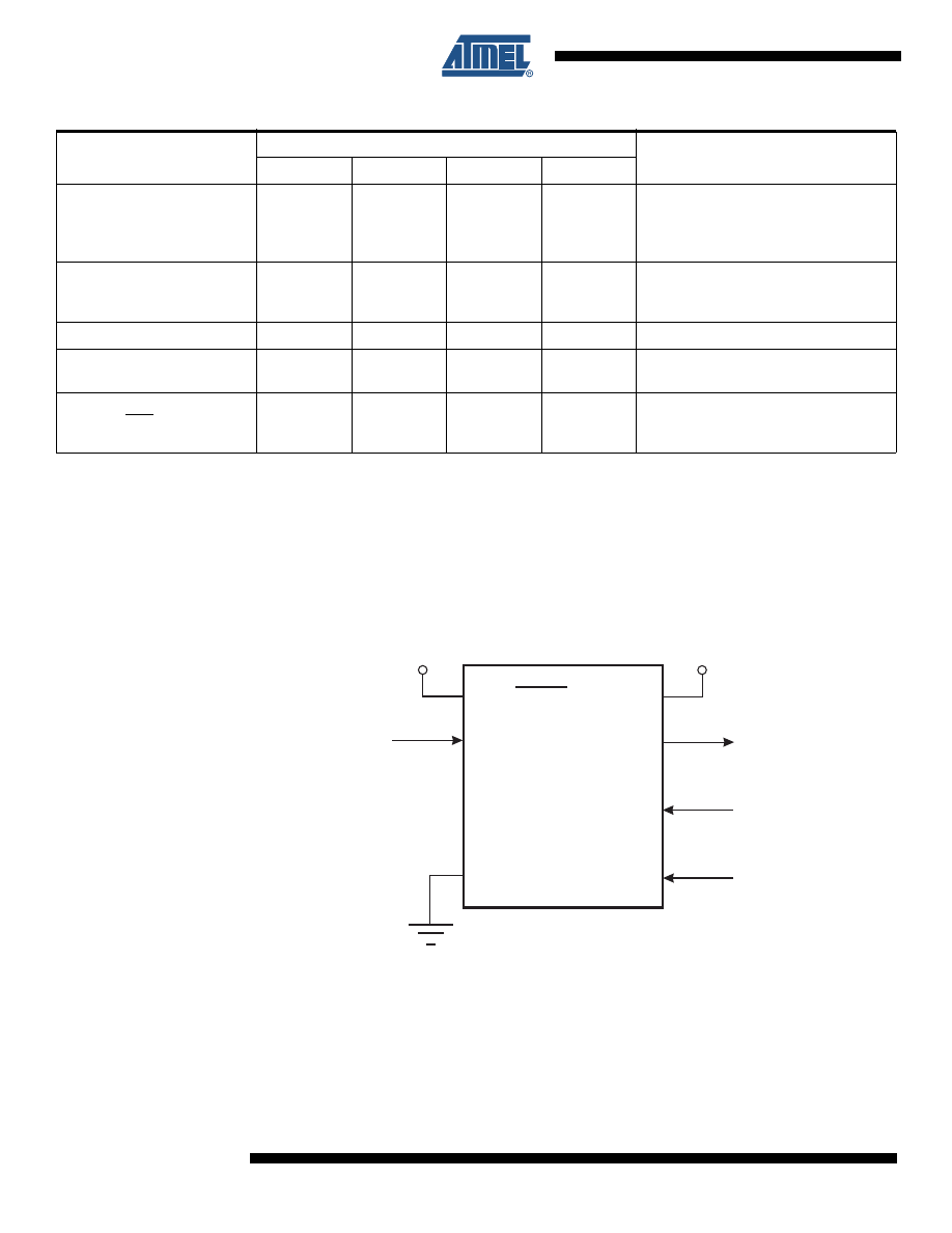
108
2535J–AVR–08/10
ATtiny13
Note:
a = address high bits, b = address low bits, H = 0 - Low byte, 1 - High Byte, o = data out, i = data in, x = don’t care
17.7 High-Voltage Serial Programming
This section describes how to program and verify Flash Program memory, EEPROM Data mem-
ory, lock bits and fuse bits in the ATtiny13.
Figure 17-2. High-voltage Serial Programming
Read Fuse Byte
0101 H000
0000 H000
xxxx xxxx
oooo oooo
Read fuse low/high byte. Bit “0” =
programmed, “1” = unprogrammed.
See
for
details.
Write Fuse Byte
1010 1100
1010 H000
xxxx xxxx
iiii iiii
Set fuse low/high byte. Set bit to “0” to
program, “1” to unprogram. See
for details.
Read Signature Byte
0011 0000
000x xxxx
xxxx xxbb
oooo oooo
Read Signature Byte o at address b.
Read Calibration Byte
0011 1000
000x xxxx
0000 000b
oooo oooo
Read Calibration Byte. See
“Calibration Bytes” on page 104
Poll RDY/BSY
1111 0000
0000 0000
xxxx xxxx
xxxx xxxo
If o = “1”, a programming operation is
still busy. Wait until this bit returns to
“0” before applying another command.
Table 17-9.
Serial Programming Instruction Set (Continued)
Instruction
Instruction Format
Operation
Byte 1
Byte 2
Byte 3
Byte4
VCC
GND
SDO
SII
SDI
(RESET)
+1.8 - 5.5V
PB0
PB1
PB2
PB5
+11.5 - 12.5V
PB3
SCI
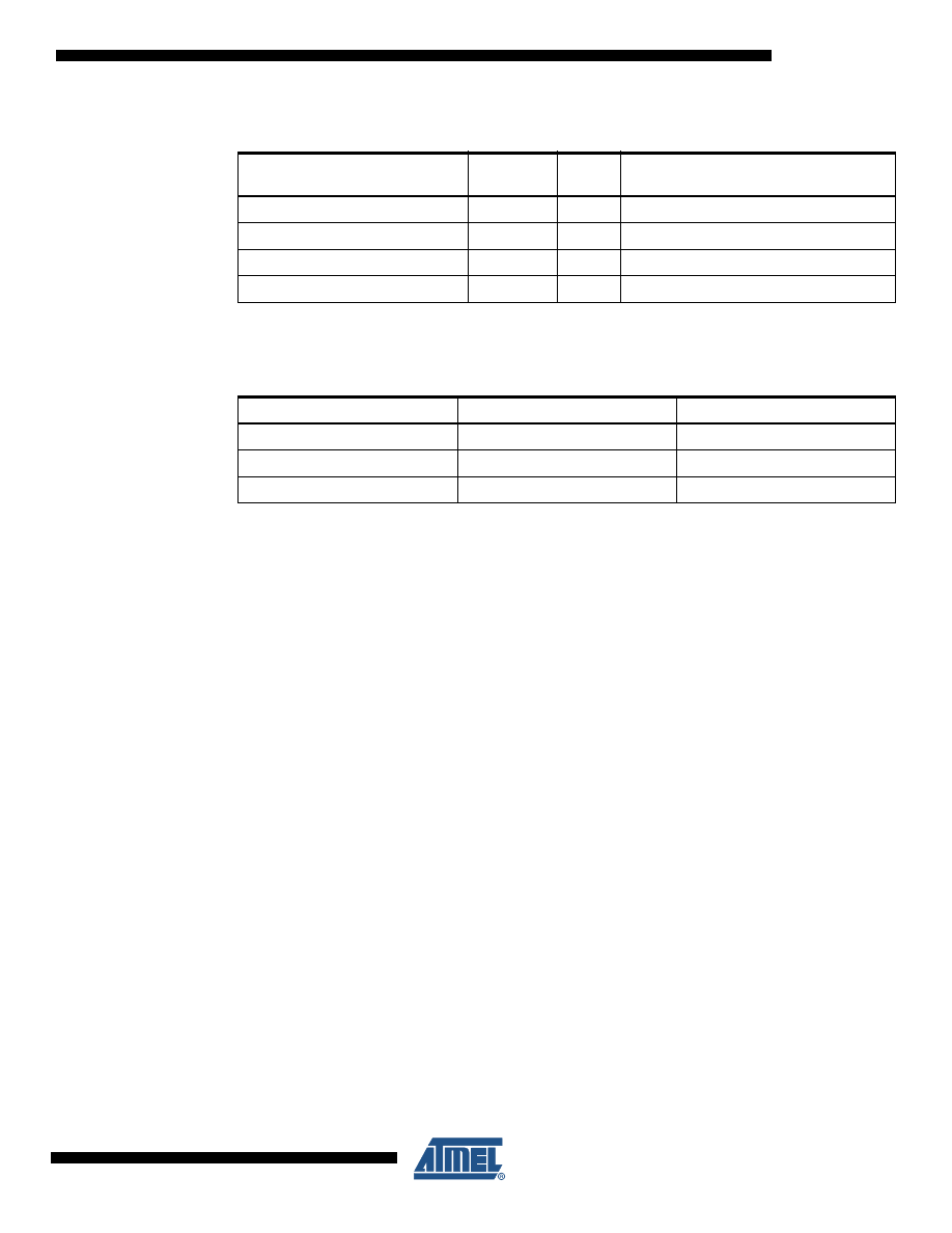
109
2535J–AVR–08/10
ATtiny13
The minimum period for the Serial Clock Input (SCI) during High-voltage Serial Programming is
220 ns.
17.7.1
High-Voltage Serial Programming Algorithm
To program and verify the ATtiny13 in the High-voltage Serial Programming mode, the following
sequence is recommended (See instruction formats in
The following algorithm puts the device in High-voltage Serial Programming mode:
1. Set Prog_enable pins listed in
to “000”, RESET pin to “0” and Vcc to 0V.
2. Apply 4.5 - 5.5V between VCC and GND. Ensure that Vcc reaches at least 1.8V within
the next 20µs.
3. Wait 20 - 60µs, and apply 11.5 - 12.5V to RESET.
4. Keep the Prog_enable pins unchanged for at least 10µs after the High-voltage has
been applied to ensure the Prog_enable Signature has been latched.
5. Release the Prog_enable[2] pin to avoid drive contention on the Prog_enable[2]/SDO
pin.
6. Wait at least 300µs before giving any serial instructions on SDI/SII.
7. Exit Programming mode by power the device down or by bringing RESET pin to 0V.
If the rise time of the Vcc is unable to fulfill the requirements listed above, the following alterna-
tive algorithm can be used.
1. Set Prog_enable pins listed in
to “000”, RESET pin to “0” and Vcc to 0V.
2. Apply 4.5 - 5.5V between VCC and GND.
3. Monitor Vcc, and as soon as Vcc reaches 0.9 - 1.1V, apply 11.5 - 12.5V to RESET.
4. Keep the Prog_enable pins unchanged for at least 10µs after theHigh-voltage has been
applied to ensure the Prog_enable Signature has been latched.
5. Release the Prog_enable[2] pin to avoid drive contention on the Prog_enable[2]/SDO
pin.
Table 17-10. Pin Name Mapping
Signal Name in High-voltage
Serial Programming Mode
Pin Name
I/O
Function
SDI
PB0
I
Serial Data Input
SII
PB1
I
Serial Instruction Input
SDO
PB2
O
Serial Data Output
SCI
PB3
I
Serial Clock Input (min. 220ns period)
Table 17-11. Pin Values Used to Enter Programming Mode
Pin
Symbol
Value
SDI
Prog_enable[0]
0
SII
Prog_enable[1]
0
SDO
Prog_enable[2]
0

110
2535J–AVR–08/10
ATtiny13
6. Wait until Vcc actually reaches 4.5 - 5.5V before giving any serialinstructions on
SDI/SII.
7. Exit Programming mode by power the device down or by bringing RESET pin to 0V.
17.7.2
High-Voltage Serial Programming Instruction set
The instruction set is described in
.
Table 17-12. High-voltage Reset Characteristics
Supply Voltage
RESET Pin High-voltage Threshold
Minimum High-voltage Period for
Latching Prog_enable
V
CC
V
HVRST
t
HVRST
4.5V
12V
100 ns
5.5V
12
100 ns
Table 17-13. High-Voltage Serial Programming Instruction Set for ATtiny13
Instruction
Instruction Format
Operation Remarks
Instr.1/5
Instr.2/6
Instr.3
Instr.4
Chip Erase
SDI
SII
SDO
0_1000_0000_00
0_0100_1100_00
x_xxxx_xxxx_xx
0_0000_0000_00
0_0110_0100_00
x_xxxx_xxxx_xx
0_0000_0000_00
0_0110_1100_00
x_xxxx_xxxx_xx
Wait after Instr.3 until SDO goes
high for the Chip Erase cycle to
finish.
Load “Write
Flash”
Command
SDI
SII
SDO
0_0001_0000_00
0_0100_1100_00
x_xxxx_xxxx_xx
Enter Flash Programming code.
Load Flash
Page Buffer
SDI
SII
SDO
0_ bbbb_bbbb _00
0_0000_1100_00
x_xxxx_xxxx_xx
0_eeee_eeee_00
0_0010_1100_00
x_xxxx_xxxx_xx
0_dddd_dddd_00
0_0011_1100_00
x_xxxx_xxxx_xx
0_0000_0000_00
0_0111_1101_00
x_xxxx_xxxx_xx
Repeat after Instr. 1 - 5 until the
entire page buffer is filled or until all
data within the page is filled. See
Note 1.
SDI
SII
SDO
0_0000_0000_00
0_0111_1100_00
x_xxxx_xxxx_xx
Instr 5.
Load Flash High
Address and
Program Page
SDI
SII
SDO
0_0000_000a_00
0_0001_1100_00
x_xxxx_xxxx_xx
0_0000_0000_00
0_0110_0100_00
x_xxxx_xxxx_xx
0_0000_0000_00
0_0110_1100_00
x_xxxx_xxxx_xx
Wait after Instr 3 until SDO goes
high. Repeat Instr. 2 - 3 for each
loaded Flash Page until the entire
Flash or all data is programmed.
Repeat Instr. 1 for a new 256 byte
page. See Note 1.
Load “Read
Flash”
Command
SDI
SII
SDO
0_0000_0010_00
0_0100_1100_00
x_xxxx_xxxx_xx
Enter Flash Read mode.
Read Flash Low
and High Bytes
SDI
SII
SDO
0_bbbb_bbbb_00
0_0000_1100_00
x_xxxx_xxxx_xx
0_0000_000a_00
0_0001_1100_00
x_xxxx_xxxx_xx
0_0000_0000_00
0_0110_1000_00
x_xxxx_xxxx_xx
0_0000_0000_00
0_0110_1100_00
q_qqqq_qqqx_xx
Repeat Instr. 1, 3 - 6 for each new
address. Repeat Instr. 2 for a new
256 byte page.
SDI
SII
SDO
0_0000_0000_00
0_0111_1000_00
x_xxxx_xxxx_xx
0_0000_0000_00
0_0111_1100_00
p_pppp_pppx_xx
Instr 5 - 6.
Load “Write
EEPROM”
Command
SDI
SII
SDO
0_0001_0001_00
0_0100_1100_00
x_xxxx_xxxx_xx
Enter EEPROM Programming
mode.

111
2535J–AVR–08/10
ATtiny13
Load EEPROM
Page Buffer
SDI
SII
SDO
0_00bb_bbbb_00
0_0000_1100_00
x_xxxx_xxxx_xx
0_eeee_eeee_00
0_0010_1100_00
x_xxxx_xxxx_xx
0_0000_0000_00
0_0110_1101_00
x_xxxx_xxxx_xx
0_0000_0000_00
0_0110_1100_00
x_xxxx_xxxx_xx
Repeat Instr. 1 - 4 until the entire
page buffer is filled or until all data
within the page is filled. See Note
2.
Program
EEPROM Page
SDI
SII
SDO
0_0000_0000_00
0_0110_0100_00
x_xxxx_xxxx_xx
0_0000_0000_00
0_0110_1100_00
x_xxxx_xxxx_xx
Wait after Instr. 2 until SDO goes
high. Repeat Instr. 1 - 2 for each
loaded EEPROM page until the
entire EEPROM or all data is
programmed.
Write EEPROM
Byte
SDI
SII
SDO
0_00bb_bbbb_00
0_0000_1100_00
x_xxxx_xxxx_xx
0_eeee_eeee_00
0_0010_1100_00
x_xxxx_xxxx_xx
0_0000_0000_00
0_0110_1101_00
x_xxxx_xxxx_xx
0_0000_0000_00
0_0110_0100_00
x_xxxx_xxxx_xx
Repeat Instr. 1 - 5 for each new
address. Wait after Instr. 5 until
SDO goes high. See Note 3.
SDI
SII
SDO
0_0000_0000_00
0_0110_1100_00
x_xxxx_xxxx_xx
Instr. 5
Load “Read
EEPROM”
Command
SDI
SII
SDO
0_0000_0011_00
0_0100_1100_00
x_xxxx_xxxx_xx
Enter EEPROM Read mode.
Read EEPROM
Byte
SDI
SII
SDO
0_bbbb_bbbb_00
0_0000_1100_00
x_xxxx_xxxx_xx
0_aaaa_aaaa_00
0_0001_1100_00
x_xxxx_xxxx_xx
0_0000_0000_00
0_0110_1000_00
x_xxxx_xxxx_xx
0_0000_0000_00
0_0110_1100_00
q_qqqq_qqq0_00
Repeat Instr. 1, 3 - 4 for each new
address. Repeat Instr. 2 for a new
256 byte page.
Write Fuse Low
Bits
SDI
SII
SDO
0_0100_0000_00
0_0100_1100_00
x_xxxx_xxxx_xx
0_A987_6543_00
0_0010_1100_00
x_xxxx_xxxx_xx
0_0000_0000_00
0_0110_0100_00
x_xxxx_xxxx_xx
0_0000_0000_00
0_0110_1100_00
x_xxxx_xxxx_xx
Wait after Instr. 4 until SDO goes
high. Write A - 3 = “0” to program
the Fuse bit.
Write Fuse High
Bits
SDI
SII
SDO
0_0100_0000_00
0_0100_1100_00
x_xxxx_xxxx_xx
0_000F_EDCB_00
0_0010_1100_00
x_xxxx_xxxx_xx
0_0000_0000_00
0_0111_0100_00
x_xxxx_xxxx_xx
0_0000_0000_00
0_0111_1100_00
x_xxxx_xxxx_xx
Wait after Instr. 4 until SDO goes
high. Write F - B = “0” to program
the Fuse bit.
Write Lock Bits
SDI
SII
SDO
0_0010_0000_00
0_0100_1100_00
x_xxxx_xxxx_xx
0_0000_0021_00
0_0010_1100_00
x_xxxx_xxxx_xx
0_0000_0000_00
0_0110_0100_00
x_xxxx_xxxx_xx
0_0000_0000_00
0_0110_1100_00
x_xxxx_xxxx_xx
Wait after Instr. 4 until SDO goes
high. Write 2 - 1 = “0” to program
the Lock Bit.
Read Fuse Low
Bits
SDI
SII
SDO
0_0000_0100_00
0_0100_1100_00
x_xxxx_xxxx_xx
0_0000_0000_00
0_0110_1000_00
x_xxxx_xxxx_xx
0_0000_0000_00
0_0110_1100_00
A_9876_543x_xx
Reading A - 3 = “0” means the
Fuse bit is programmed.
Read Fuse High
Bits
SDI
SII
SDO
0_0000_0100_00
0_0100_1100_00
x_xxxx_xxxx_xx
0_0000_0000_00
0_0111_1010_00
x_xxxx_xxxx_xx
0_0000_0000_00
0_0111_1110_00
x_xxFE_DCBx_xx
Reading F - B = “0” means the fuse
bit is programmed.
Read Lock Bits
SDI
SII
SDO
0_0000_0100_00
0_0100_1100_00
x_xxxx_xxxx_xx
0_0000_0000_00
0_0111_1000_00
x_xxxx_xxxx_xx
0_0000_0000_00
0_0111_1100_00
x_xxxx_x21x_xx
Reading 2, 1 = “0” means the lock
bit is programmed.
Table 17-13. High-Voltage Serial Programming Instruction Set for ATtiny13 (Continued)
Instruction
Instruction Format
Operation Remarks
Instr.1/5
Instr.2/6
Instr.3
Instr.4

112
2535J–AVR–08/10
ATtiny13
Note:
a = address high bits, b = address low bits, d = data in high bits, e = data in low bits, p = data out high bits, q = data out low bits,
x = don’t care, 1 = Lock Bit1, 2 = Lock Bit2, 3 = CKSEL0 fuse, 4 = CKSEL1 fuse, 5 = SUT0 fuse, 6 = SUT1 fuse, 7 = CKDIV8,
fuse, 8 = WDTON fuse, 9 = EESAVE fuse, A = SPIEN fuse, B = RSTDISBL fuse, C = BODLEVEL0 fuse, D= BODLEVEL1 fuse,
E = MONEN fuse, F = SELFPRGEN fuse
Note:
The EEPROM is written page-wise. But only the bytes that are loaded into the page are actually written to the EEPROM. Page-
wise EEPROM access is more efficient when multiple bytes are to be written to the same page. Note that auto-erase of
EEPROM is not available in High-voltage Serial Programming, only in SPI Programming.
17.8 Considerations for Efficient Programming
The loaded command and address are retained in the device during programming. For efficient
programming, the following should be considered.
• The command needs only be loaded once when writing or reading multiple memory
locations.
• Skip writing the data value 0xFF that is the contents of the entire EEPROM (unless the
EESAVE fuse is programmed) and Flash after a Chip Erase.
• Address High byte needs only be loaded before programming or reading a new 256 word
window in Flash or 256 byte EEPROM. This consideration also applies to Signature bytes
reading.
17.8.1
Chip Erase
The Chip Erase will erase the Flash and EEPROM
memories plus lock bits. The lock bits are
not reset until the Program memory has been completely erased. The fuse bits are not changed.
A Chip Erase must be performed before the Flash and/or EEPROM are re-programmed.
1. Load command “Chip Erase” (see
2. Wait after Instr. 3 until SDO goes high for the “Chip Erase” cycle to finish.
3. Load Command “No Operation”.
Note:
1. The EEPROM memory is preserved during Chip Erase if the EESAVE fuse is programmed.
Read Signature
Bytes
SDI
SII
SDO
0_0000_1000_00
0_0100_1100_00
x_xxxx_xxxx_xx
0_0000_00bb_00
0_0000_1100_00
x_xxxx_xxxx_xx
0_0000_0000_00
0_0110_1000_00
x_xxxx_xxxx_xx
0_0000_0000_00
0_0110_1100_00
q_qqqq_qqqx_xx
Repeats Instr 2 4 for each
signature byte address.
Read
Calibration Byte
SDI
SII
SDO
0_0000_1000_00
0_0100_1100_00
x_xxxx_xxxx_xx
0_0000_000b_00
0_0000_1100_00
x_xxxx_xxxx_xx
0_0000_0000_00
0_0111_1000_00
x_xxxx_xxxx_xx
0_0000_0000_00
0_0111_1100_00
p_pppp_pppx_xx
Load “No
Operation”
Command
SDI
SII
SDO
0_0000_0000_00
0_0100_1100_00
x_xxxx_xxxx_xx
Table 17-13. High-Voltage Serial Programming Instruction Set for ATtiny13 (Continued)
Instruction
Instruction Format
Operation Remarks
Instr.1/5
Instr.2/6
Instr.3
Instr.4
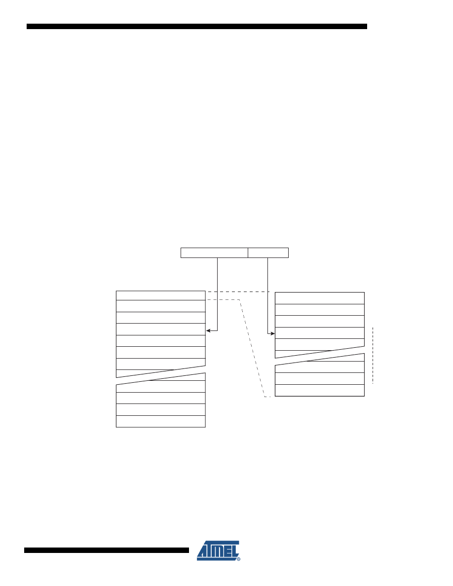
113
2535J–AVR–08/10
ATtiny13
17.8.2
Programming the Flash
The Flash is organized in pages, see
. When programming the Flash,
the program data is latched into a page buffer. This allows one page of program data to be pro-
grammed simultaneously. The following procedure describes how to program the entire Flash
memory:
1. Load Command “Write Flash” (see
2. Load Flash Page Buffer.
3. Load Flash High Address and Program Page. Wait after Instr. 3 until SDO goes high for
the “Page Programming” cycle to finish.
4. Repeat 2 through 3 until the entire Flash is programmed or until all data has been
programmed.
5. End Page Programming by Loading Command “No Operation”.
When writing or reading serial data to the ATtiny13, data is clocked on the rising edge of the
serial clock, see
and
for details.
Figure 17-3. Addressing the Flash which is Organized in Pages
PROGRAM MEMORY
WORD ADDRESS
WITHIN A PAGE
PAGE ADDRESS
WITHIN THE FLASH
INSTRUCTION WORD
PAGE
PCWORD[PAGEMSB:0]:
00
01
02
PAGEEND
PAGE
PCWORD
PCPAGE
PCMSB
PAGEMSB
PROGRAM
COUNTER
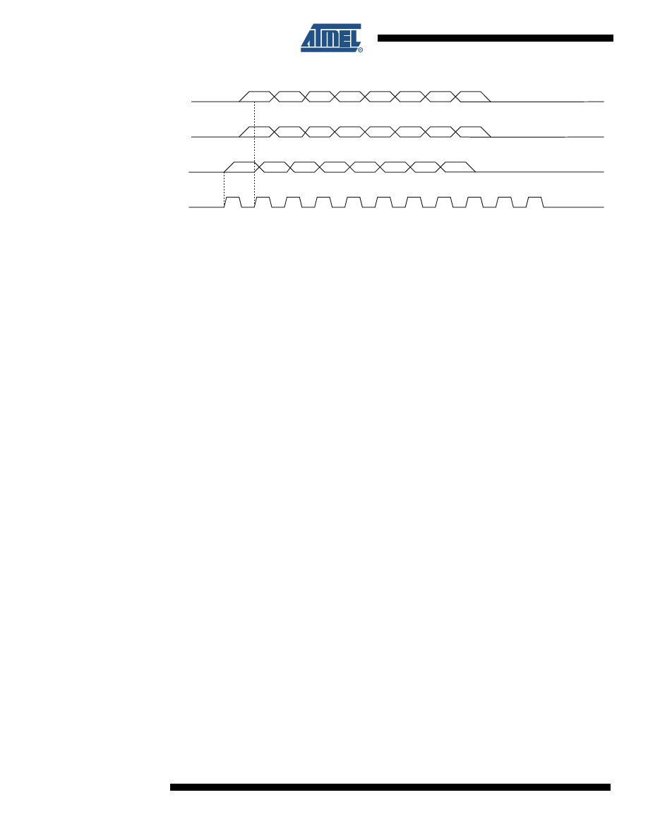
114
2535J–AVR–08/10
ATtiny13
Figure 17-4. High-voltage Serial Programming Waveforms
17.8.3
Programming the EEPROM
The EEPROM is organized in pages, see
. When programming the
EEPROM, the data is latched into a page buffer. This allows one page of data to be pro-
grammed simultaneously. The programming algorithm for the EEPROM Data memory is as
follows (refer to
1. Load Command “Write EEPROM”.
2. Load EEPROM Page Buffer.
3. Program EEPROM Page. Wait after Instr. 2 until SDO goes high for the “Page Pro-
gramming” cycle to finish.
4. Repeat 2 through 3 until the entire EEPROM is programmed or until all data has been
programmed.
5. End Page Programming by Loading Command “No Operation”.
17.8.4
Reading the Flash
The algorithm for reading the Flash memory is as follows (refer to
):
1. Load Command "Read Flash".
2. Read Flash Low and High Bytes. The contents at the selected address are available at
serial output SDO.
17.8.5
Reading the EEPROM
The algorithm for reading the EEPROM memory is as follows (refer to
1. Load Command “Read EEPROM”.
2. Read EEPROM Byte. The contents at the selected address are available at serial out-
put SDO.
17.8.6
Programming and Reading the Fuse and Lock Bits
The algorithms for programming and reading the fuse low/high bits and lock bits are shown in
MSB
MSB
MSB
LSB
LSB
LSB
0
1
2
3
4
5
6
7
8
9
10
SDI
PB0
SII
PB1
SDO
PB2
SCI
PB3

115
2535J–AVR–08/10
ATtiny13
17.8.7
Reading the Signature Bytes and Calibration Byte
The algorithms for reading the Signature bytes and Calibration byte are shown in
.
17.8.8
Power-off sequence
Set SCI to “0”. Set RESET to “1”. Turn V
CC
power off.
18. Electrical Characteristics
18.1 Absolute Maximum Ratings*
18.2 DC Characteristics
Operating Temperature.................................. -55
°C to +125°C
*NOTICE:
Stresses beyond those listed under “Absolute
Maximum Ratings” may cause permanent dam-
age to the device. This is a stress rating only and
functional operation of the device at these or
other conditions beyond those indicated in the
operational sections of this specification is not
implied. Exposure to absolute maximum rating
conditions for extended periods may affect
device reliability.
Storage Temperature ..................................... -65°C to +150°C
Voltage on any Pin except RESET
with respect to Ground ................................-0.5V to V
CC
+0.5V
Voltage on RESET with respect to Ground......-0.5V to +13.0V
Maximum Operating Voltage ............................................ 6.0V
DC Current per I/O Pin ............................................... 40.0 mA
DC Current V
CC
and GND Pins ................................ 200.0 mA
Table 18-1.
DC Characteristics, T
A
= -40
°C to +85°C
Symbol
Parameter
Condition
Min.
Typ.
Max.
Units
V
IL
Input Low Voltage,
Any Pin as I/O
V
CC
= 1.8V - 2.4V
-0.5
0.2V
CC
V
V
CC
= 2.4V - 5.5V
-0.5
0.3V
CC
V
Input Low Voltage,
RESET Pin as Reset
V
CC
= 1.8V - 5.5
-0.5
0.2V
CC
V
V
IH
Input High Voltage,
Any Pin as I/O
V
CC
= 1.8V - 2.4V
0.7V
CC
V
CC
+ 0.5
V
V
CC
= 2.4V - 5.5V
0.6V
V
CC
+ 0.5
V
Input High Voltage,
RESET Pin as Reset
V
CC
= 1.8V - 5.5V
0.9V
CC
V
CC
+ 0.5
V
V
OL
Output Low Voltage,
Pins PB0 and PB1
I
OL
= 20 mA, V
CC
= 5V
0.7
V
I
OL
= 10 mA, V
CC
= 3V
0.5
V
Output Low Voltage,
Pins PB2, PB3 and PB4
I
OL
= 10 mA, V
CC
= 5V
0.7
V
I
OL
= 5 mA, V
CC
= 3V
0.5
V
V
OH
Output High Voltage,
Pins PB0 and PB1
I
OH
= -20 mA, V
CC
= 5V
4.2
V
I
OH
= -10 mA, V
CC
= 3V
2.5
V
Output High Voltage,
Pins PB2, PB3 and PB4
I
OH
= -10 mA, V
CC
= 5V
4.2
V
I
OH
= -5 mA, V
CC
= 3V
2.5
V
I
LIL
Input Leakage
Current I/O Pin
V
CC
= 5.5V, pin low
-1
1
µA

116
2535J–AVR–08/10
ATtiny13
Notes: 1. Typical values at +25
°C.
2. “Max” means the highest value where the pin is guaranteed to be read as low.
3. Not tested in production.
4. “Min” means the lowest value where the pin is guaranteed to be read as high.
5. Although each I/O port can under non-transient, steady state conditions sink more than the test conditions, the sum of all I
OL
(for all ports) should not exceed 60 mA. If I
OL
exceeds the test condition, V
OL
may exceed the related specification. Pins are
not guaranteed to sink current greater than the listed test condition.
6. Although each I/O port can under non-transient, steady state conditions source more than the test conditions, the sum of all
I
OH
(for all ports) should not exceed 60 mA. If I
OH
exceeds the test condition, V
OH
may exceed the related specification. Pins
are not guaranteed to source current greater than the listed test condition.
I
LIH
Input Leakage
Current I/O Pin
V
CC
= 5.5V, pin high
-1
1
µA
R
PU
Pull-Up Resistor, I/O Pin
V
CC
= 5.5V, input low
20
50
k
Ω
Pull-Up Resistor, Reset Pin
V
CC
= 5.5V, input low
30
80
k
Ω
I
CC
Supply Current,
Active Mode
f = 1MHz, V
CC
= 2V
0.3
0.35
mA
f = 4MHz, V
CC
= 3V
1.6
1.8
mA
f = 8MHz, V
CC
= 5V
5
6
mA
Supply Current,
Idle Mode
f = 1MHz, V
CC
= 2V
0.08
0.2
mA
f = 4MHz, V
CC
= 3V
0.41
1
mA
f = 8MHz, V
CC
= 5V
1.6
3
mA
Supply Current,
Power-Down Mode
WDT enabled, V
CC
= 3V
5
10
µA
WDT disabled, V
CC
= 3V
0.5
2
µA
Table 18-1.
DC Characteristics, T
A
= -40
°C to +85°C (Continued)
Symbol
Parameter
Condition
Min.
Typ.
(1)
Max.
Units
117
2535J–AVR–08/10
ATtiny13
18.3 Speed Grades
The maximum operating frequency of the device depends on V
CC.
As shown in
and
, the maximum frequency vs. V
CC
relationship is linear between 1.8V < V
CC
< 2.7V
and between 2.7V < V
CC
< 4.5V.
Figure 18-1. Maximum Frequency vs. V
CC
for ATtiny13V
Figure 18-2. Maximum Frequency vs. V
CC
for ATtiny13
10 MHz
4 MHz
1.8V
2.7V
5.5V
Safe Operating Area
20 MHz
10 MHz
2.7V
4.5V
5.5V
Safe Operating Area
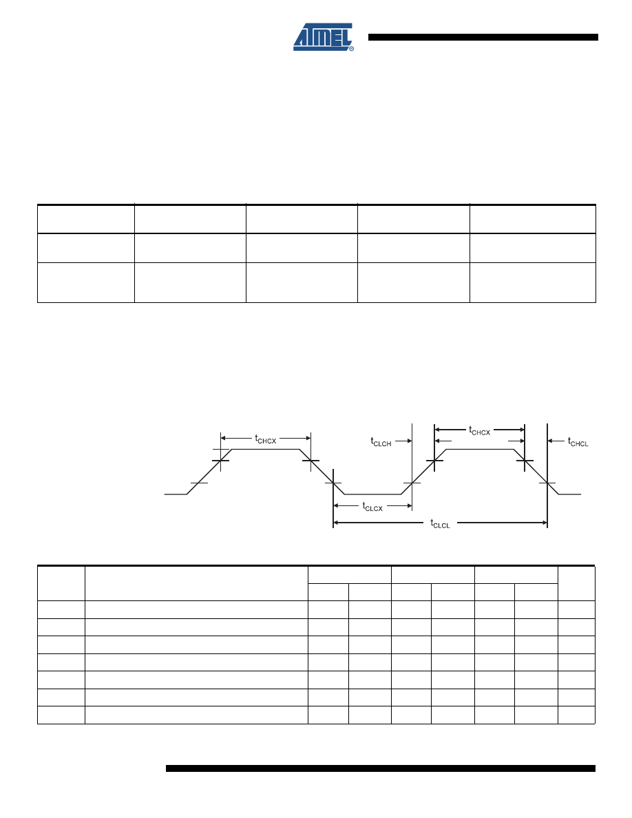
118
2535J–AVR–08/10
ATtiny13
18.4 Clock Characteristics
18.4.1
Calibrated Internal RC Oscillator Accuracy
It is possible to manually calibrate the internal oscillator to be more accurate than default factory
calibration. Note that the oscillator frequency depends on temperature and voltage. Voltage and
temperature characteristics can be found in
,
,
,
, and
.
Notes: 1. Accuracy of oscillator frequency at calibration point (fixed temperature and fixed voltage).
2. Voltage range for ATtiny13V.
3. Voltage range for ATtiny13.
18.4.2
External Clock Drive
Figure 18-3. External Clock Drive Waveform
Table 18-2.
Calibration Accuracy of Internal RC Oscillator
Calibration
Method
Target Frequency
V
CC
Temperature
Accuracy at given Voltage
& Temperature
Factory
Calibration
4.8 / 9.6 MHz
3V
25
°C
±10%
User
Calibration
Fixed frequency within:
4 – 5 MHz / 8 – 10 MHz
Fixed voltage within:
1.8V – 5.5V
2.7V – 5.5V
Fixed temperature
within:
-40
°C to +85°C
±2%
V
IL1
V
IH1
Table 18-3.
External Clock Drive
Symbol
Parameter
V
CC
= 1.8 - 5.5V
V
CC
= 2.7 - 5.5V
V
CC
= 4.5 - 5.5V
Units
Min.
Max.
Min.
Max.
Min.
Max.
1/t
CLCL
Clock Frequency
0
4
0
10
0
20
MHz
t
CLCL
Clock Period
250
100
50
ns
t
CHCX
High Time
100
40
20
ns
t
CLCX
Low Time
100
40
20
ns
t
CLCH
Rise Time
2.0
1.6
0.5
µs
t
CHCL
Fall Time
2.0
1.6
0.5
µs
Δ
t
CLCL
Change in period from one clock cycle to the next
2
2
2
%
119
2535J–AVR–08/10
ATtiny13
18.5 System and Reset Characteristics
Note:
1. The Power-on Reset will not work unless the supply voltage has been below V
POT
(falling)
18.5.1
Brown-Out Detection
Note:
1. V
BOT
may be below nominal minimum operating voltage for some devices. For devices where
this is the case, the device is tested down to V
CC
= V
BOT
during the production test. This guar-
antees that a Brown-out Reset will occur before V
CC
drops to a voltage where correct
operation of the microcontroller is no longer guaranteed.
18.6 Analog Comparator Characteristics
Note:
All parameters are based on simulation results and they are not tested in production
Table 18-4.
Reset, Brown-out and Internal Voltage Reference Characteristics
Symbol
Parameter
Condition
Min
Typ
Max
Units
V
POT
Power-on Reset Threshold Voltage (rising)
T
A
= -40 to +85
°C
1.2
V
Power-on Reset Threshold Voltage
(falling)
T
A
= -40 to +85
°C
1.1
V
V
RST
RESET Pin Threshold Voltage
V
CC
= 1.8V - 5.5V
0.2 V
CC
0.9 V
CC
V
t
RST
Minimum pulse width on RESET Pin
V
CC
= 1.8V - 5.5V
2.5
µs
V
HYST
Brown-out Detector Hysteresis
50
mV
t
BOD
Min Pulse Width on Brown-out Reset
2
µs
V
BG
Bandgap reference voltage
1.0
1.1
1.2
V
t
BG
Bandgap reference start-up time
40
70
µs
I
BG
Bandgap reference current consumption
15
µs
Table 18-5.
V
BOT
vs. BODLEVEL Fuse Coding
BODLEVEL [1:0] Fuses
Min
Typ
Max
Units
11
BOD Disabled
10
1.8
V
01
2.7
00
4.3
Table 18-6.
Analog Comparator Characteristics, T
A
= -40
°C to +85°C
Symbol
Parameter
Condition
Min
Typ
Max
Units
V
AIO
Input Offset Voltage
V
CC
= 5V, V
IN
= V
CC
/ 2
< 10
40
mV
I
LAC
Input Leakage Current
V
CC
= 5V, V
IN
= V
CC
/ 2
-50
50
nA
t
APD
Analog Propagation Delay
(from saturation to slight overdrive)
V
CC
= 2.7V
750
ns
V
CC
= 4.0V
500
Analog Propagation Delay
(large step change)
V
CC
= 2.7V
100
V
CC
= 4.0V
75
t
DPD
Digital Propagation Delay
V
CC
= 1.8V - 5.5
1
2
CLK

120
2535J–AVR–08/10
ATtiny13
18.7 ADC Characteristics
Table 18-7.
ADC Characteristics, Single Ended Channels. T
A
= -40
°C to +85°C
Symbol
Parameter
Condition
Min
Typ
Max
Units
Resolution
10
Bits
Absolute accuracy
(Including INL, DNL, and
Quantization, Gain and Offset
Errors)
V
REF
= 4V, V
CC
= 4V,
ADC clock = 200 kHz
2
LSB
V
REF
= 4V, V
CC
= 4V
ADC clock = 1 MHz
3
LSB
V
REF
= 4V, V
CC
= 4V
ADC clock = 200 kHz
Noise Reduction Mode
1.5
LSB
V
REF
= 4V, V
CC
= 4V,
ADC clock = 1 MHz
Noise Reduction Mode
2.5
LSB
Integral Non-Linearity (INL)
(Accuracy after Offset and
Gain Calibration)
V
REF
= 4V, V
CC
= 4V
ADC clock = 200 kHz
1
LSB
Differential Non-linearity
(DNL)
V
REF
= 4V, V
CC
= 4V
ADC clock = 200 kHz
0.5
LSB
Gain Error
V
REF
= 4V, V
CC
= 4V
ADC clock = 200 kHz
2.5
LSB
Offset Error
V
REF
= 4V, V
CC
= 4V
ADC clock = 200 kHz
1.5
LSB
Conversion Time
Free Running Conversion
13
260
µs
Clock Frequency
50
1000
kHz
V
IN
Input Voltage
GND
V
REF
V
Input Bandwidth
38.5
kHz
V
INT
Internal Voltage Reference
1.0
1.1
1.2
V
R
AIN
Analog Input Resistance
100
M
Ω
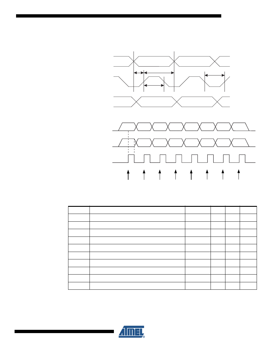
121
2535J–AVR–08/10
ATtiny13
18.8 Serial Programming Characteristics
Figure 18-4. Serial Programming Timing
Figure 18-5. Serial Programming Waveform
Note:
1. 2 t
CLCL
for f
ck
< 12 MHz, 3 t
CLCL
for f
ck
>= 12 MHz
Table 18-8.
Serial Programming Characteristics, T
A
= -40
°C to +85°C, V
CC
= 1.8 - 5.5V
(Unless Otherwise Noted)
Symbol
Parameter
Min
Typ
Max
Units
1/t
CLCL
Oscillator Frequency (ATtiny13V, V
CC
= 1.8 - 5.5V)
0
1
MHz
t
CLCL
Oscillator Period (ATtiny13V, V
CC
= 1.8 - 5.5V)
1000
ns
1/t
CLCL
Oscillator Frequency (ATtiny13, V
CC
= 2.7 - 5.5V)
0
9.6
MHz
t
CLCL
Oscillator Period (ATtiny13, V
CC
= 2.7 - 5.5V)
104
ns
1/t
CLCL
Oscillator Frequency (ATtiny13, V
CC
= 4.5V - 5.5V)
0
20
MHz
t
CLCL
Oscillator Period (ATtiny13, V
CC
= 4.5V - 5.5V)
50
ns
t
SHSL
SCK Pulse Width High
2 t
CLCL
ns
t
SLSH
SCK Pulse Width Low
2 t
CLCL
ns
t
OVSH
MOSI Setup to SCK High
t
CLCL
ns
t
SHOX
MOSI Hold after SCK High
2 t
CLCL
ns
MOSI
MISO
SCK
t
OVSH
t
SHSL
t
SLSH
t
SHOX
MSB
MSB
LSB
LSB
SERIAL CLOCK INPUT
(SCK)
SERIAL DATA INPUT
(MOSI)
(MISO)
SAMPLE
SERIAL DATA OUTPUT
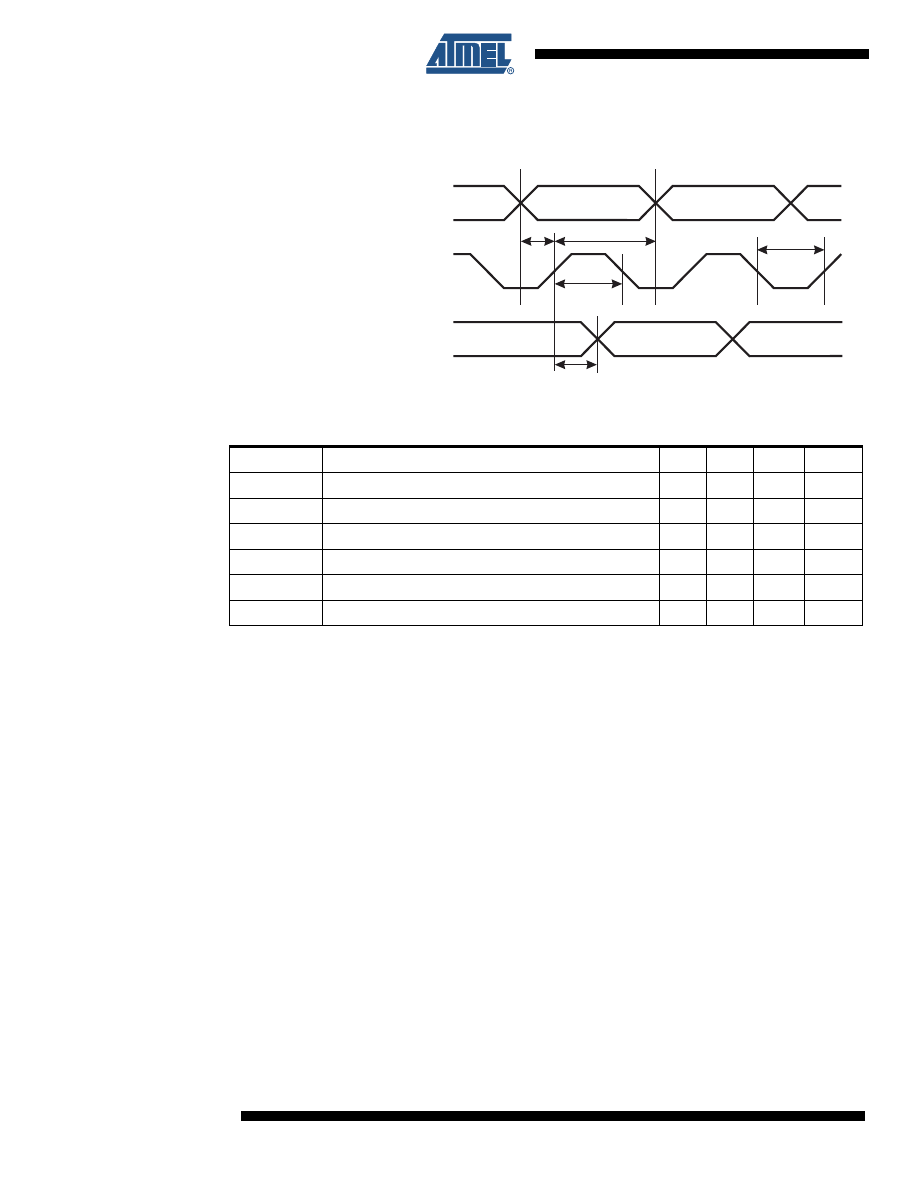
122
2535J–AVR–08/10
ATtiny13
18.9 High-voltage Serial Programming Characteristics
Figure 18-6. High-voltage Serial Programming Timing
Table 18-9.
High-voltage Serial Programming Characteristics
T
A
= 25
°C, V
CC
= 5.0V ± 10% (Unless otherwise noted)
Symbol
Parameter
Min
Typ
Max
Units
t
SHSL
SCI (PB3) Pulse Width High
110
ns
t
SLSH
SCI (PB3) Pulse Width Low
110
ns
t
IVSH
SDI (PB0), SII (PB1) Valid to SCI (PB3) High
50
ns
t
SHIX
SDI (PB0), SII (PB1) Hold after SCI (PB3) High
50
ns
t
SHOV
SCI (PB3) High to SDO (PB2) Valid
16
ns
t
WLWH_PFB
Wait after Instr. 3 for Write Fuse Bits
2.5
ms
SDI (PB0), SII (PB1)
SDO (PB2)
SCI (PB3)
t
IVSH
t
SHSL
t
SLSH
t
SHIX
t
SHOV

123
2535J–AVR–08/10
ATtiny13
19. Typical Characteristics
The data contained in this section is largely based on simulations and characterization of similar
devices in the same process and design methods. Thus, the data should be treated as indica-
tions of how the part will behave.
The following charts show typical behavior. These figures are not tested during manufacturing.
During characterisation devices are operated at frequencies higher than test limits but they are
not guaranteed to function properly at frequencies higher than the ordering code indicates.
All current consumption measurements are performed with all I/O pins configured as inputs and
with internal pull-ups enabled. Current consumption is a function of several factors such as oper-
ating voltage, operating frequency, loading of I/O pins, switching rate of I/O pins, code executed
and ambient temperature. The dominating factors are operating voltage and frequency.
A sine wave generator with rail-to-rail output is used as clock source but current consumption in
Power-Down mode is independent of clock selection. The difference between current consump-
tion in Power-Down mode with Watchdog Timer enabled and Power-Down mode with Watchdog
Timer disabled represents the differential current drawn by the Watchdog Timer.
The current drawn from pins with a capacitive load may be estimated (for one pin) as follows:
where V
CC
= operating voltage, C
L
= load capacitance and f
SW
= average switching frequency of
I/O pin.
19.1 Active Supply Current
Figure 19-1. Active Supply Current vs. Frequency (0.1 - 1.0 MHz)
I
CP
V
CC
C
L
f
×
×
SW
≈
ACTIVE SUPPLY CURRENT vs. LOW FREQUENCY
0.1 - 1.0 MH
z
5.5 V
5.0 V
4.5 V
4.0 V
3.3 V
2.7 V
1.8 V
0
0.2
0.4
0.6
0.8
1
1.2
0
0.1
0.2
0.3
0.4
0.5
0.6
0.7
0.8
0.9
1
Frequency (MHz)
I
CC
(m
A
)
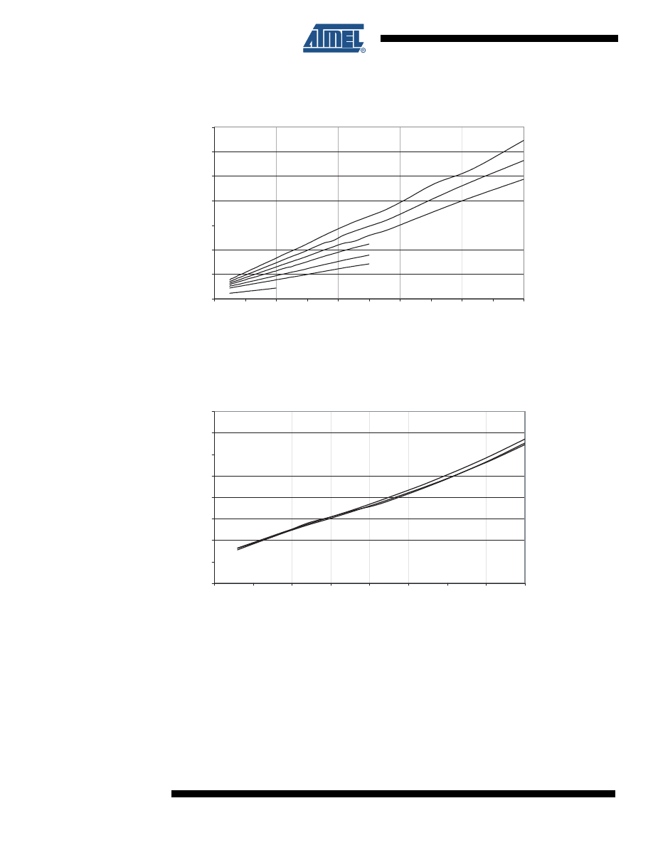
124
2535J–AVR–08/10
ATtiny13
Figure 19-2. Active Supply Current vs. Frequency (1 - 20 MHz)
Figure 19-3. Active Supply Current vs. V
CC
(Internal RC Oscillator, 9.6 MHz)
ACTIVE SUPPLY CURRENT vs. FREQUENCY
1 - 20MH
z
5.5 V
5.0 V
4.5 V
4.0 V
3.3 V
2.7 V
1.8 V
0
2
4
6
8
10
12
14
0
2
4
6
8
10
12
14
16
18
20
Frequency (MHz)
I
CC
(m
A
)
ACTIVE SUPPLY CURRENT vs. V
CC
INTERNAL RC OSCILLATOR, 9.6 MH
z
85 °C
25 °C
-40 °C
0
1
2
3
4
5
6
7
8
1.5
2
2.5
3
3.5
4
4.5
5
5.5
V
CC
(V)
I
CC
(mA)

125
2535J–AVR–08/10
ATtiny13
Figure 19-4. Active Supply Current vs. V
CC
(Internal RC Oscillator, 4.8 MHz)
Figure 19-5. Active Supply Current vs. V
CC
(Internal WDT Oscillator, 128 kHz)
ACTIVE SUPPLY CURRENT vs. V
CC
INTERNAL RC OSCILLATOR, 4.8 MH
z
85 °C
25 °C
-40 °C
0
0.5
1
1.5
2
2.5
3
3.5
4
4.5
1.5
2
2.5
3
3.5
4
4.5
5
5.5
V
CC
(V)
I
CC
(mA)
ACTIVE SUPPLY CURRENT vs. V
CC
INTERNAL WD OSCILLATOR, 128 KHz
85 °C
25 °C
-40 °C
0
0.02
0.04
0.06
0.08
0.1
0.12
0.14
1.5
2
2.5
3
3.5
4
4.5
5
5.5
V
CC
(V)
I
CC
(mA)
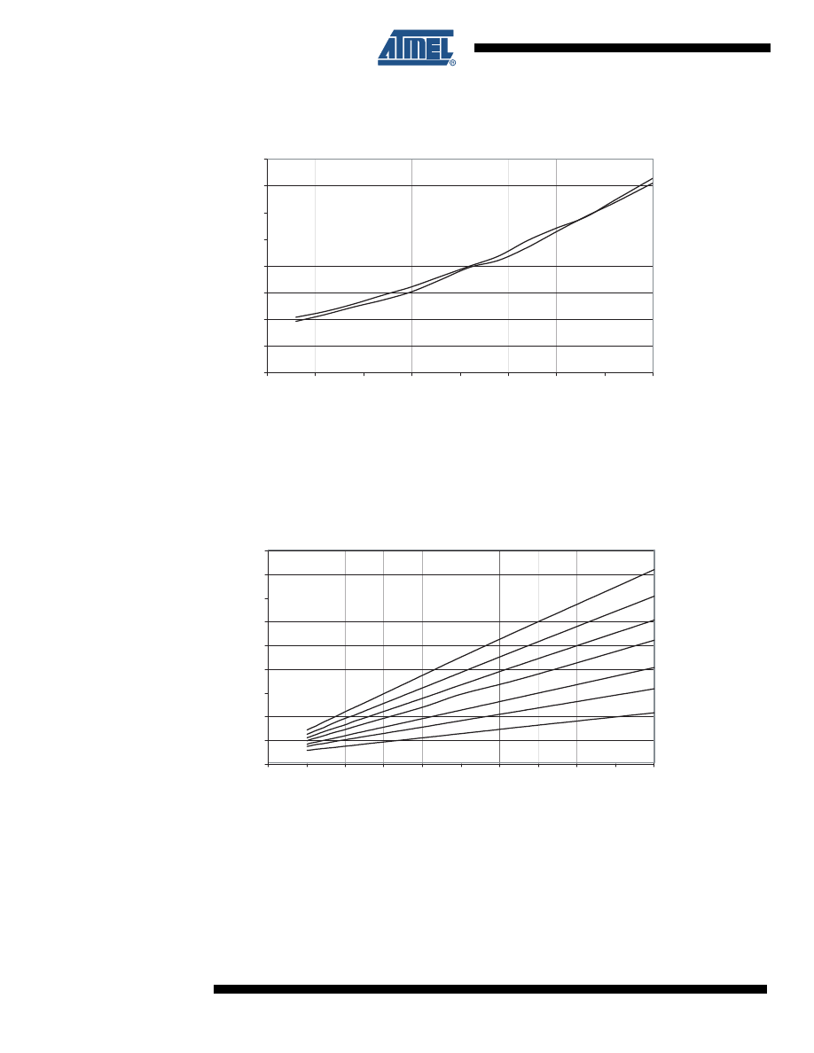
126
2535J–AVR–08/10
ATtiny13
Figure 19-6. Active Supply Current vs. V
CC
(32 kHz External Clock)
19.2 Idle Supply Current
Figure 19-7. Idle Supply Current vs. Frequency (0.1 - 1.0 MHz)
ACTIVE SUPPLY CURRENT vs. V
CC
32 kHz EXTERNAL CLOCK
85 °C
25 °C
0
0.005
0.01
0.015
0.02
0.025
0.03
0.035
0.04
1.5
2
2.5
3
3.5
4
4.5
5
5.5
V
CC
(V)
I
CC
(mA)
IDLE SUPPLY CURRENT vs. LOW FREQUENCY
(0.1 - 1.0 MHz)
5.5 V
5.0 V
4.5 V
4.0 V
3.3 V
2.7 V
1.8 V
0
0.1
0.2
0.3
0.4
0.5
0.6
0.7
0.8
0.9
0
0.1
0.2
0.3
0.4
0.5
0.6
0.7
0.8
0.9
1
Frequency (MHz)
I
CC
(mA)
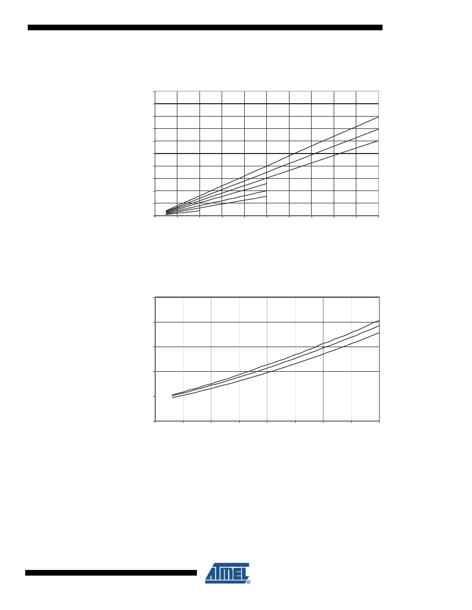
127
2535J–AVR–08/10
ATtiny13
Figure 19-8. Idle Supply Current vs. Frequency (1 - 20 MHz)
Figure 19-9. Idle Supply Current vs. V
CC
(Internal RC Oscillator, 9.6 MHz)
IDLE SUPPLY CURRENT vs. FREQUENCY
1 - 20MHz
5.5 V
5.0 V
4.5 V
4.0 V
3.3 V
2.7 V
1.8 V
0
0.5
1
1.5
2
2.5
3
3.5
4
4.5
5
0
2
4
6
8
10
12
14
16
18
20
Frequency (MHz)
I
CC
(mA)
IDLE SUPPLY CURRENT vs. V
CC
INTERNAL RC OSCILLATOR, 9.6 MH
z
85 °C
25 °C
-40 °C
0
0.5
1
1.5
2
2.5
1.5
2
2.5
3
3.5
4
4.5
5
5.5
V
CC
(V)
I
CC
(mA)

128
2535J–AVR–08/10
ATtiny13
Figure 19-10. Idle Supply Current vs. V
CC
(Internal RC Oscillator, 4.8 MHz)
Figure 19-11. Idle Supply Current vs. V
CC
(Internal RC Oscillator, 128 kHz)
IDLE SUPPLY CURRENT vs. V
CC
INTERNAL RC OSCILLATOR, 4.8 MH
z
85 °C
25 °C
-40 °C
0
0.2
0.4
0.6
0.8
1
1.2
1.5
2
2.5
3
3.5
4
4.5
5
5.5
V
CC
(V)
I
CC
(mA)
IDLE SUPPLY CURRENT vs. V
CC
INTERNAL WD OSCILLATOR, 128 KH
z
85 °C
25 °C
-40 °C
0
0.005
0.01
0.015
0.02
0.025
0.03
0.035
1.5
2
2.5
3
3.5
4
4.5
5
5.5
V
CC
(V)
I
CC
(mA)
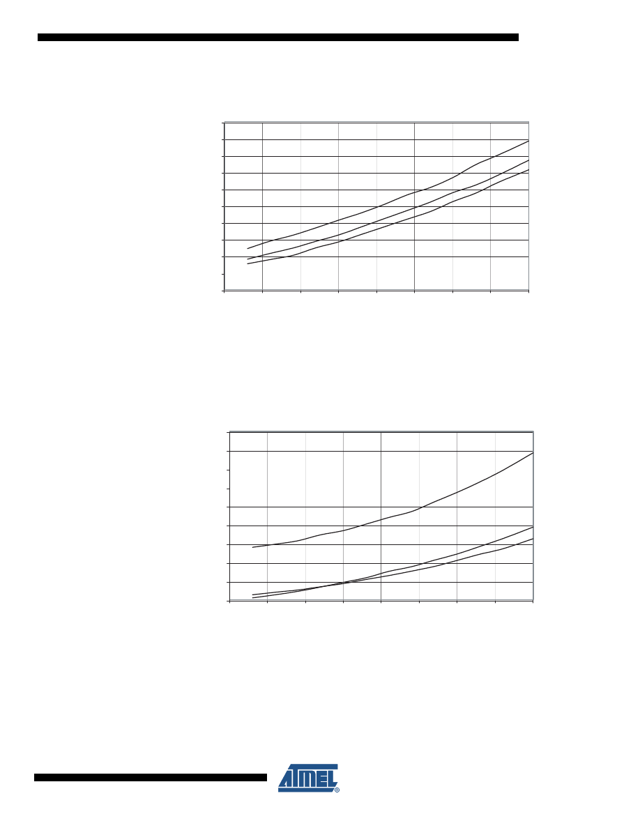
129
2535J–AVR–08/10
ATtiny13
Figure 19-12. Idle Supply Current vs. V
CC
(32 kHz External Clock)
19.3 Power-Down Supply Current
Figure 19-13. Power-Down Supply Current vs. V
CC
(Watchdog Timer Disabled)
IDLE SUPPLY CURRENT vs. V
CC
32kHz EXTERNAL CLOCK
85 °C
25 °C
-40 °C
0
1
2
3
4
5
6
7
8
9
10
1.5
2
2.5
3
3.5
4
4.5
5
5.5
V
CC
(V)
I
CC
(uA)
POWER-DOWN SUPPLY CURRENT vs. V
CC
WATCHDOG TIMER DISABLED
85 ˚C
25 ˚C
-40 ˚C
0
0.2
0.4
0.6
0.8
1
1.2
1.4
1.6
1.8
1.5
2
2.5
3
3.5
4
4.5
5
5.5
V
CC
(V)
I
CC
(uA)
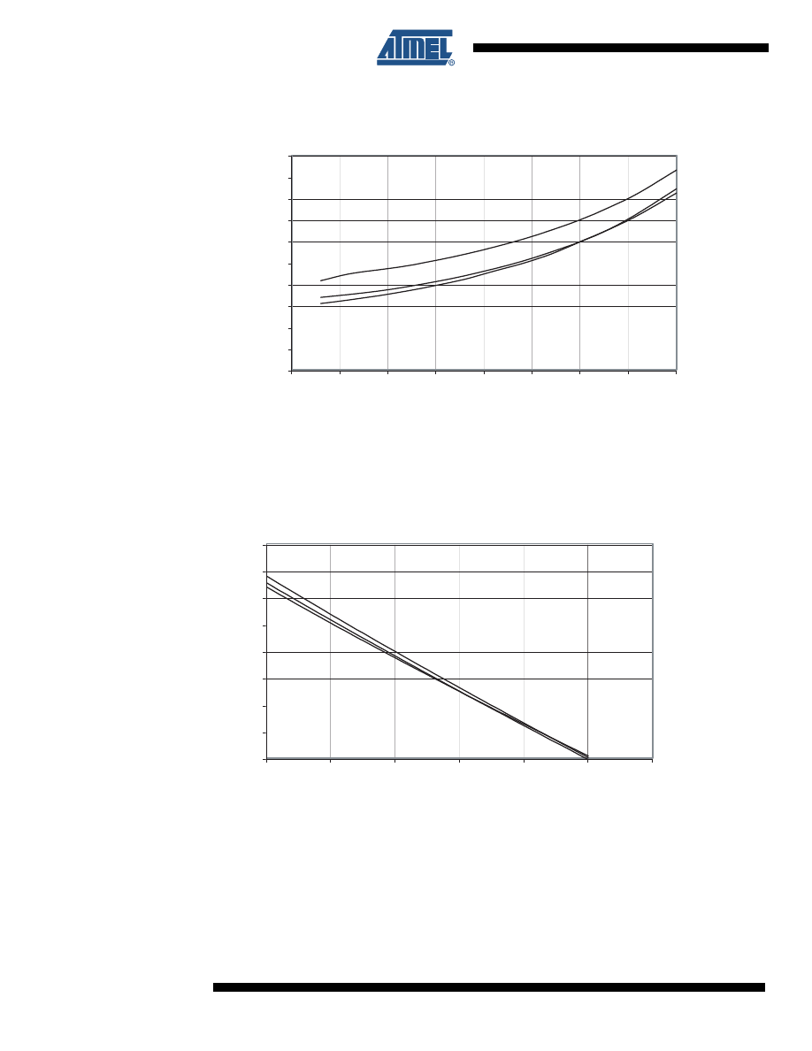
130
2535J–AVR–08/10
ATtiny13
Figure 19-14. Power-Down Supply Current vs. V
CC
(Watchdog Timer Enabled)
19.4 Pin Pull-up
Figure 19-15. I/O Pin Pull-up Resistor Current vs. Input Voltage (V
CC
= 5V)
POWER-DOWN SUPPLY CURRENT vs. V
CC
WATCHDOG TIMER ENABLED
85 ˚C
25 ˚C
-40 ˚C
0
1
2
3
4
5
6
7
8
9
10
1.5
2
2.5
3
3.5
4
4.5
5
5.5
V
CC
(V)
I
CC
(uA)
I/O PIN PULL-UP RESISTOR CURRENT vs. INPUT VOLTAGE
V
CC
= 5V
25 ˚C
-40 ˚C
0
20
40
60
80
100
120
140
160
0
1
2
3
4
5
6
V
OP
(V)
I
OP
(uA)
85 ˚C

131
2535J–AVR–08/10
ATtiny13
Figure 19-16. I/O Pin Pull-up Resistor Current vs. Input Voltage (V
CC
= 2.7V)
Figure 19-17. Reset Pull-up Resistor Current vs. Reset Pin Voltage (V
CC
= 5V)
I/O PIN PULL-UP RESISTOR CURRENT vs. INPUT VOLTAGE
V
CC
= 2.7
25 ˚C
-40 ˚C
0
10
20
30
40
50
60
70
80
0
0.5
1
1.5
2
2.5
3
V
OP
(V)
I
OP
(uA)
85 ºC
RESET PULL-UP RESISTOR CURRENT vs. RESET PIN VOLTAGE
V
CC
= 5V
85 ˚C
25 ˚C
-40 ˚C
0
20
40
60
80
100
120
0
1
2
3
4
5
V
RESET
(V)
I
RESET
(uA)
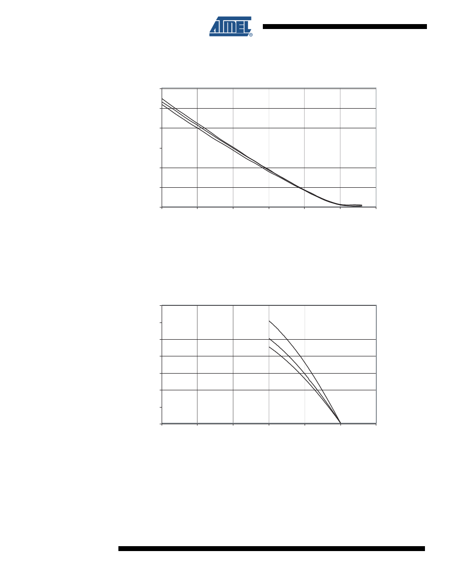
132
2535J–AVR–08/10
ATtiny13
Figure 19-18. Reset Pull-up Resistor Current vs. Reset Pin Voltage (V
CC
= 2.7V)
19.5 Pin Driver Strength
Figure 19-19. I/O Pin Source Current vs. Output Voltage (Low Power Ports, V
CC
= 5V)
RESET PULL-UP RESISTOR CURRENT vs. RESET PIN VOLTAGE
V
CC
= 2.7V
85 ˚C
25 ˚C
-40 ˚C
0
10
20
30
40
50
60
0
0.5
1
1.5
2
2.5
3
V
RESET
(V)
I
RESET
(uA)
I/O PIN SOURCE CURRENT vs. OUTPUT VOLTAGE
LOW POWER PORTS, V
CC
= 5V
85 ˚C
25 ˚C
-40 ˚C
0
10
20
30
40
50
60
70
0
1
2
3
4
5
6
V
OH
(V)
I
OH
(mA)
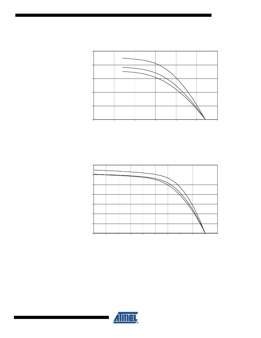
133
2535J–AVR–08/10
ATtiny13
Figure 19-20. I/O Pin Source Current vs. Output Voltage (Low Power Ports, V
CC
= 2.7V)
Figure 19-21. I/O Pin Source Current vs. Output Voltage (Low Power Ports, V
CC
= 1.8V)
I/O PIN SOURCE CURRENT vs. OUTPUT VOLTAGE
LOW POWER PORTS, V
CC
= 2.7V
85 °C
25 °C
-40 °C
0
5
10
15
20
25
0
0.5
1
1.5
2
2.5
3
V
OH
(V)
I
OH
(mA)
I/O PIN SOURCE CURRENT vs. OUTPUT VOLTAGE
LOW POWER PORTS, V
CC
= 1.8V
85 ˚C
25 ˚C
-40 ˚C
0
1
2
3
4
5
6
7
0
0.2
0.4
0.6
0.8
1
1.2
1.4
1.6
1.8
2
V
OH
(V)
I
OH
(mA)
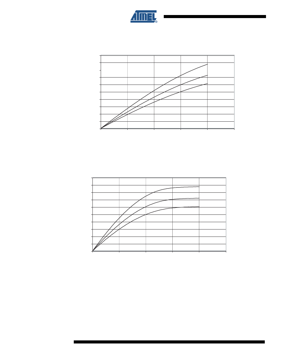
134
2535J–AVR–08/10
ATtiny13
Figure 19-22. I/O Pin Sink Current vs. Output Voltage (Low Power Ports, V
CC
= 5V)
Figure 19-23. I/O Pin Sink Current vs. Output Voltage (Low Power Ports, V
CC
= 2.7V)
I/O PIN SINK CURRENT vs. OUTPUT VOLTAGE
LOW POWER PORTS, V
CC
= 5V
85 ˚C
25 ˚C
-40 ˚C
0
5
10
15
20
25
30
35
40
45
50
0
0.5
1
1.5
2
2.5
V
OL
(V)
I
OL
(mA)
I/O PIN SINK CURRENT vs. OUTPUT VOLTAGE
Low Power Ports, V
CC
= 2.7V
85 ˚C
25 ˚C
-40 ˚C
0
2
4
6
8
10
12
14
16
18
20
0
0.5
1
1.5
2
2.5
V
OL
(V)
I
OL
(mA)
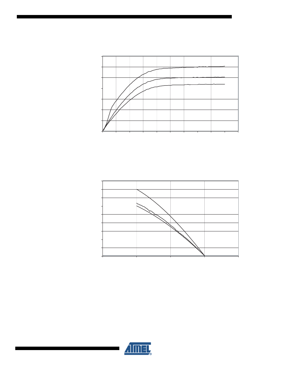
135
2535J–AVR–08/10
ATtiny13
Figure 19-24. I/O Pin Sink Current vs. Output Voltage (Low Power Ports, V
CC
= 1.8V)
Figure 19-25. I/O Pin Source Current vs. Output Voltage (V
CC
= 5V)
I/O PIN SINK CURRENT vs. OUTPUT VOLTAGE
LOW POWER PORTS, 1.8V
85 ˚C
25 ˚C
-40 ˚C
0
1
2
3
4
5
6
7
0
0.2
0.4
0.6
0.8
1
1.2
1.4
1.6
1.8
2
V
OL
(V)
I
OL
(mA)
I/O PIN SOURCE CURRENT vs. OUTPUT VOLTAGE
V
CC
= 5V
85 ˚C
25 ˚C
-40 ˚C
0
10
20
30
40
50
60
70
80
90
2
3
4
5
6
V
OH
(V)
I
OH
(mA)
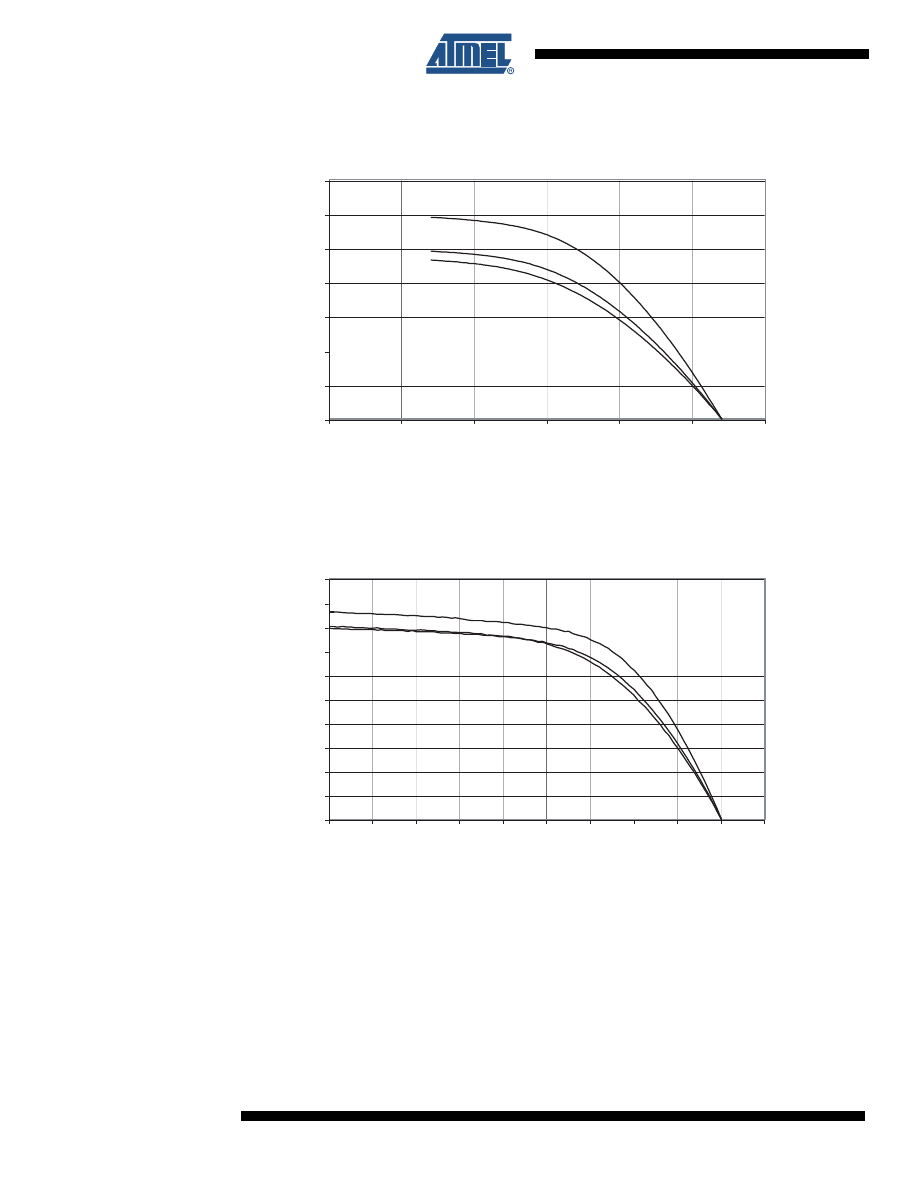
136
2535J–AVR–08/10
ATtiny13
Figure 19-26. I/O Pin Source Current vs. Output Voltage (V
CC
= 2.7V)
Figure 19-27. I/O Pin Source Current vs. Output Voltage (V
CC
= 1.8V)
I/O PIN SOURCE CURRENT vs. OUTPUT VOLTAGE
V
CC
= 2.7V
85 ˚C
25 ˚C
-40 ˚C
0
5
10
15
20
25
30
35
0
0.5
1
1.5
2
2.5
3
V
OH
(V)
I
OH
(mA)
I/O PIN SOURCE CURRENT vs. OUTPUT VOLTAGE
V
CC
= 1.8V
85 ˚C
25 ˚C
-40 ˚C
0
1
2
3
4
5
6
7
8
9
10
0
0.2
0.4
0.6
0.8
1
1.2
1.4
1.6
1.8
2
V
OH
(V)
I
OH
(mA)
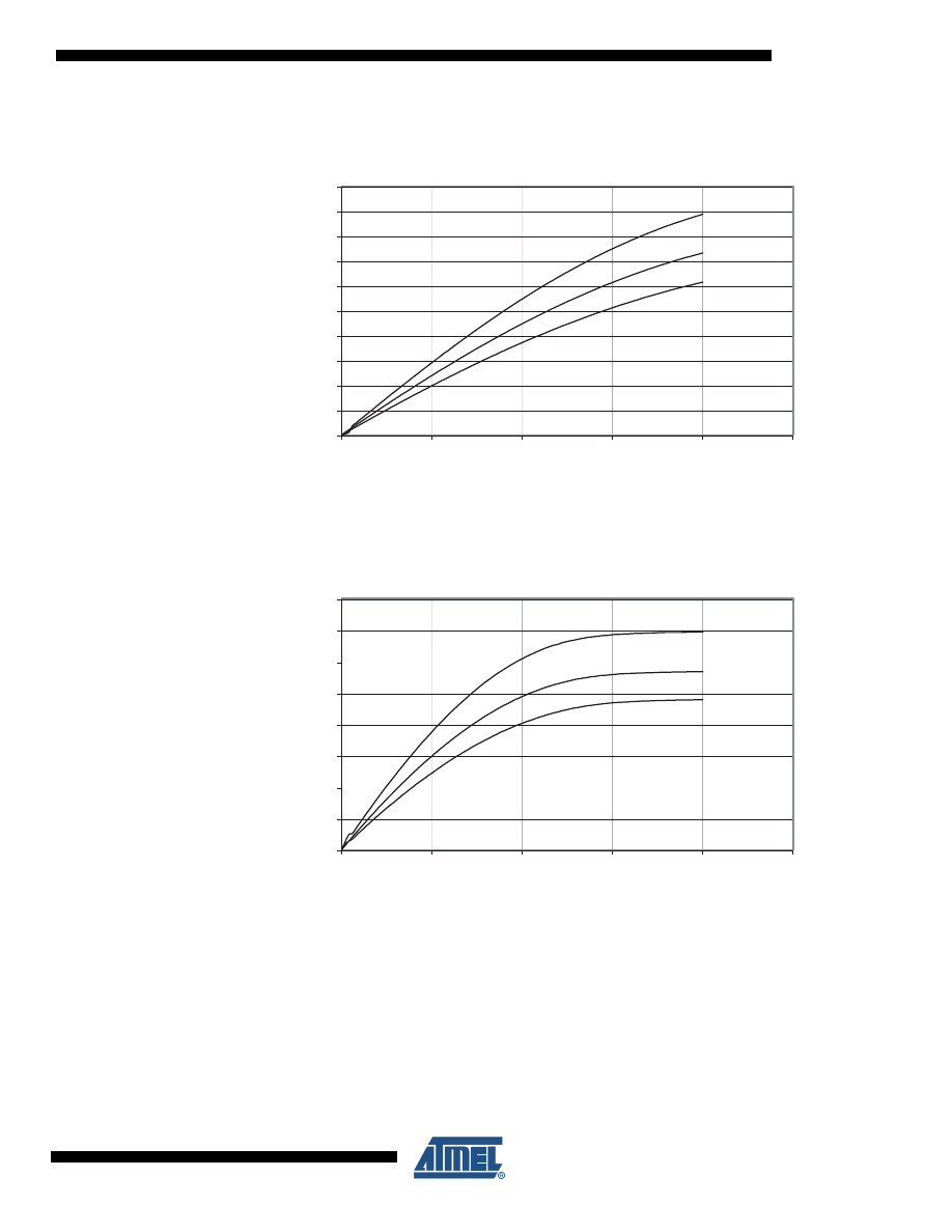
137
2535J–AVR–08/10
ATtiny13
Figure 19-28. I/O Pin Sink Current vs. Output Voltage (V
CC
= 5V)
Figure 19-29. I/O Pin Sink Current vs. Output Voltage (V
CC
= 2.7V)
I/O PIN SINK CURRENT vs. OUTPUT VOLTAGE
V
CC
= 5V
85 ˚C
25 ˚C
-40 ˚C
0
10
20
30
40
50
60
70
80
90
100
0
0.5
1
1.5
2
2.5
V
OL
(V)
I
OL
(mA)
I/O PIN SINK CURRENT vs. OUTPUT VOLTAGE
V
CC
= 2.7V
85 ˚C
25 ˚C
-40 ˚C
0
5
10
15
20
25
30
35
40
0
0.5
1
1.5
2
2.5
V
OL
(V)
I
OL
(mA)
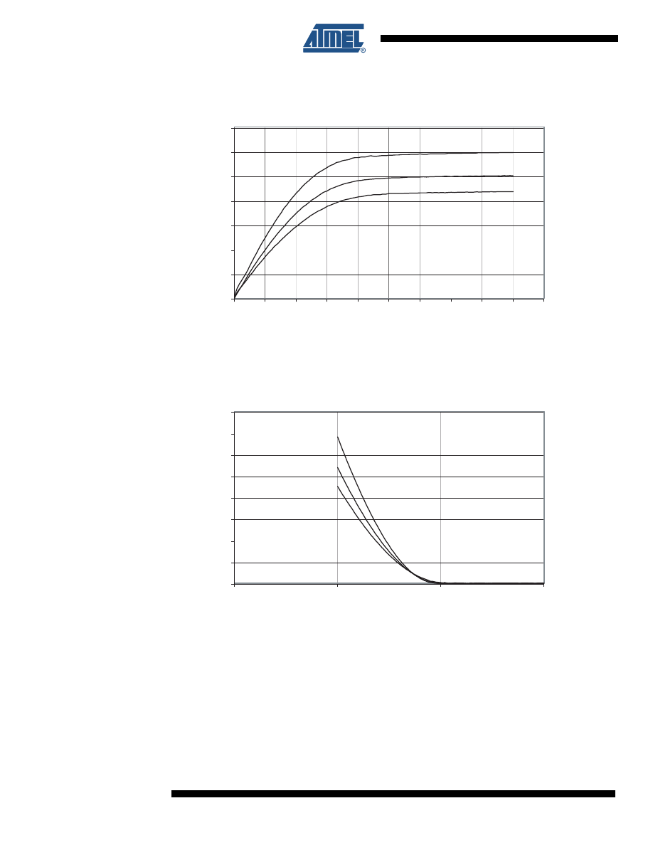
138
2535J–AVR–08/10
ATtiny13
Figure 19-30. I/O Pin Sink Current vs. Output Voltage (V
CC
= 1.8V)
Figure 19-31. Reset Pin as I/O - Source Current vs. Output Voltage (V
CC
= 5V)
I/O PIN SINK CURRENT vs. OUTPUT VOLTAGE
V
CC
= 1.8V
85 ˚C
25 ˚C
-40 ˚C
0
2
4
6
8
10
12
14
0
0.2
0.4
0.6
0.8
1
1.2
1.4
1.6
1.8
2
V
OL
(V)
I
OL
(mA)
RESET PIN AS I/O - SOURCE CURRENT vs. OUTPUT VOLTAGE
V
CC
= 5V
85 ˚C
25 ˚C
-40 ˚C
0
0.2
0.4
0.6
0.8
1
1.2
1.4
1.6
2
3
4
5
V
OH
(V)
I
OH
(mA)
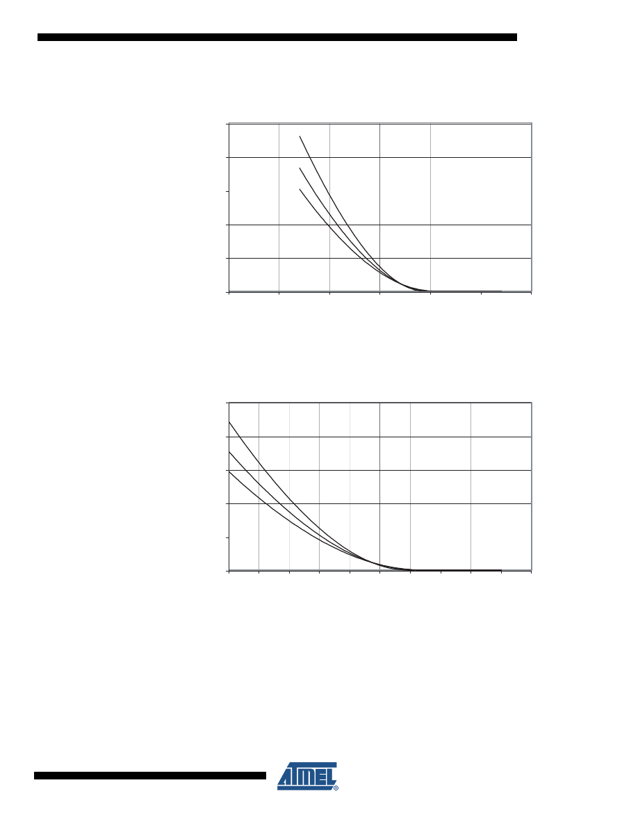
139
2535J–AVR–08/10
ATtiny13
Figure 19-32. Reset Pin as I/O - Source Current vs. Output Voltage (V
CC
= 2.7V)
Figure 19-33. Reset Pin as I/O - Source Current vs. Output Voltage (V
CC
= 1.8V)
RESET PIN AS I/O - SOURCE CURRENT vs. OUTPUT VOLTAGE
V
CC
= 2.7V
85 ˚C
25 ˚C
-40 ˚C
0
0.5
1
1.5
2
2.5
0
0.5
1
1.5
2
2.5
3
V
OH
(V)
I
OH
(mA)
RESET PIN AS I/O - SOURCE CURRENT vs. OUTPUT VOLTAGE
V
CC
= 1.8V
85 °C
25 °C
-40 °C
0
0.5
1
1.5
2
2.5
0
0.2
0.4
0.6
0.8
1
1.2
1.4
1.6
1.8
2
V
OH
(V)
I
OH
(mA)
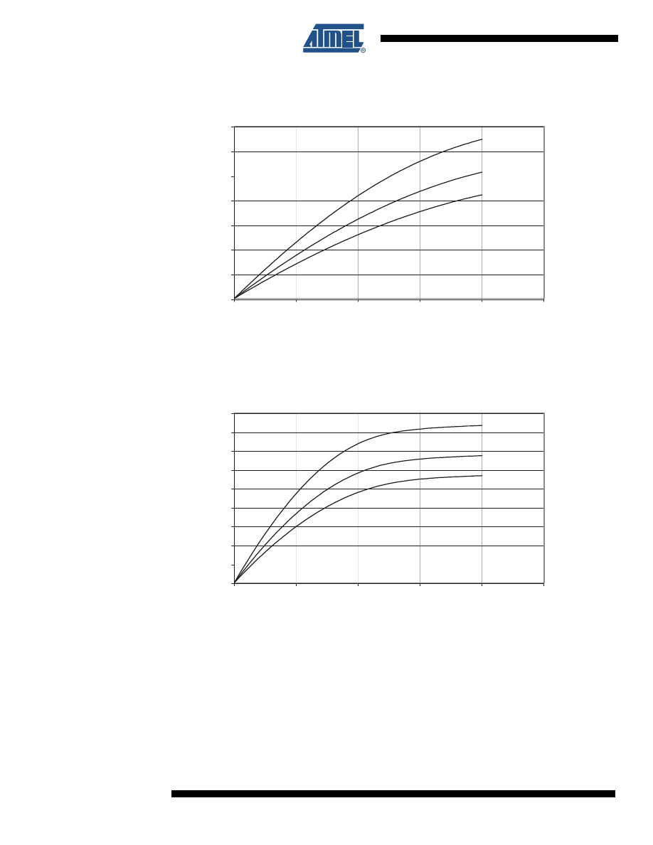
140
2535J–AVR–08/10
ATtiny13
Figure 19-34. Reset Pin as I/O - Sink Current vs. Output Voltage (V
CC
= 5V)
Figure 19-35. Reset Pin as I/O - Sink Current vs. Output Voltage (V
CC
= 2.7V)
RESET PIN AS I/O - SINK CURRENT vs. OUTPUT VOLTAGE
V
CC
= 5V
85 ˚C
25 ˚C
-40 ˚C
0
2
4
6
8
10
12
14
0
0.5
1
1.5
2
2.5
V
OL
(V)
I
OL
(mA)
RESET PIN AS I/O - SINK CURRENT vs. OUTPUT VOLTAGE
V
CC
= 2.7V
85 ˚C
25 ˚C
-40 ˚C
0
0.5
1
1.5
2
2.5
3
3.5
4
4.5
0
0.5
1
1.5
2
2.5
V
OL
(V)
I
OL
(mA)
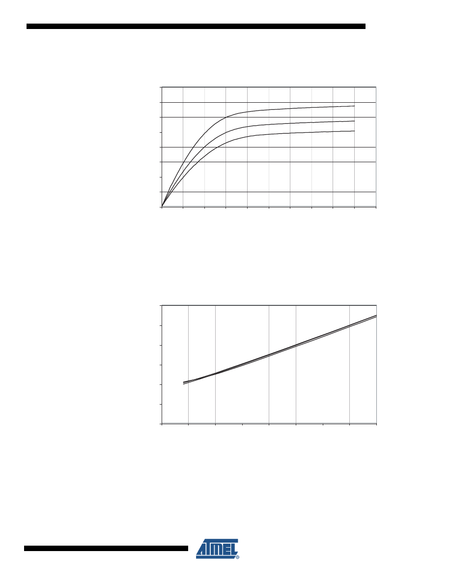
141
2535J–AVR–08/10
ATtiny13
Figure 19-36. Reset Pin as I/O - Sink Current vs. Output Voltage (V
CC
= 1.8V)
19.6 Pin Thresholds and Hysteresis
Figure 19-37. I/O Pin Input Threshold Voltage vs. V
CC
(VIH, I/O Pin Read as '1')
RESET PIN AS I/O - SINK CURRENT vs. OUTPUT VOLTAGE
V
CC
= 1.8V
85 ˚C
25 ˚C
-40 ˚C
0
0.2
0.4
0.6
0.8
1
1.2
1.4
1.6
0
0.2
0.4
0.6
0.8
1
1.2
1.4
1.6
1.8
2
V
OL
(V)
I
OL
(mA)
I/O PIN INPUT THRESHOLD VOLTAGE vs. V
CC
VIH, IO PIN READ AS '1'
85 ˚C
25 ˚C
-40 ˚C
0
0.5
1
1.5
2
2.5
3
1.5
2
2.5
3
3.5
4
4.5
5
5.5
V
CC
(V)
Threshold (V)
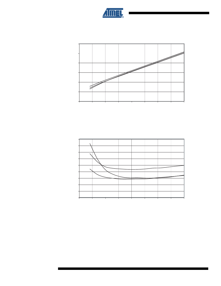
142
2535J–AVR–08/10
ATtiny13
Figure 19-38. I/O Pin Input Threshold Voltage vs. V
CC
(VIL, I/O Pin Read as '0')
Figure 19-39. I/O Pin Input Hysteresis vs. V
CC
I/O PIN INPUT THRESHOLD VOLTAGE vs. V
CC
VIL, IO PIN READ AS '0'
85 ˚C
25 ˚C
-40 ˚C
0
0.5
1
1.5
2
2.5
3
1.5
2
2.5
3
3.5
4
4.5
5
5.5
V
CC
(V)
Threshold (V)
I/O PIN INPUT HYSTERESIS vs. V
CC
0
0.05
0.1
0.15
0.2
0.25
0.3
0.35
0.4
0.45
1.5
2
2.5
3
3.5
4
4.5
5
5.5
V
CC
(V)
Input Hysteresis (V)
-40 ºC
25 ºC
85 ºC

143
2535J–AVR–08/10
ATtiny13
Figure 19-40. Reset Pin as I/O - Input Threshold Voltage vs. V
CC
(VIH, Reset Pin Read as '1')
Figure 19-41. Reset Pin as I/O - Input Threshold Voltage vs. V
CC
(VIL, Reset Pin Read as '0')
RESET PIN AS I/O - THRESHOLD VOLTAGE vs. V
CC
VIH, IO PIN READ AS '1'
85 ˚C
25 ˚C
-40 ˚C
0
0.5
1
1.5
2
2.5
3
1.5
2
2.5
3
3.5
4
4.5
5
5.5
V
CC
(V)
Threshold (V)
RESET PIN AS I/O - THRESHOLD VOLTAGE vs. V
CC
VIL, IO PIN READ AS '0'
85 ˚C
25 ˚C
-40 ˚C
0
0.5
1
1.5
2
2.5
1.5
2
2.5
3
3.5
4
4.5
5
5.5
V
CC
(V)
Threshold (V)
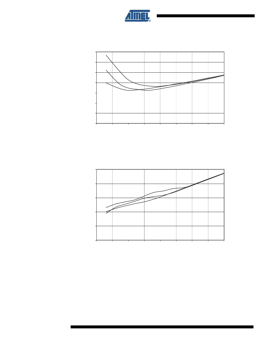
144
2535J–AVR–08/10
ATtiny13
Figure 19-42. Reset Pin as I/O - Pin Hysteresis vs. V
CC
Figure 19-43. Reset Input Threshold Voltage vs. V
CC
(VIH, Reset Pin Read as '1')
RESET PIN AS IO - PIN HYSTERESIS vs. V
CC
0
0.1
0.2
0.3
0.4
0.5
0.6
0.7
1.5
2
2.5
3
3.5
4
4.5
5
5.5
V
CC
(V)
Input Hysteresis (V)
-40 ºC
25 ºC
85 ºC
RESET INPUT THRESHOLD VOLTAGE vs. V
CC
VIH, IO PIN READ AS '1'
85 ˚C
25 ˚C
-40 ˚C
0
0.5
1
1.5
2
2.5
1.5
2
2.5
3
3.5
4
4.5
5
5.5
V
CC
(V)
Threshold (V)
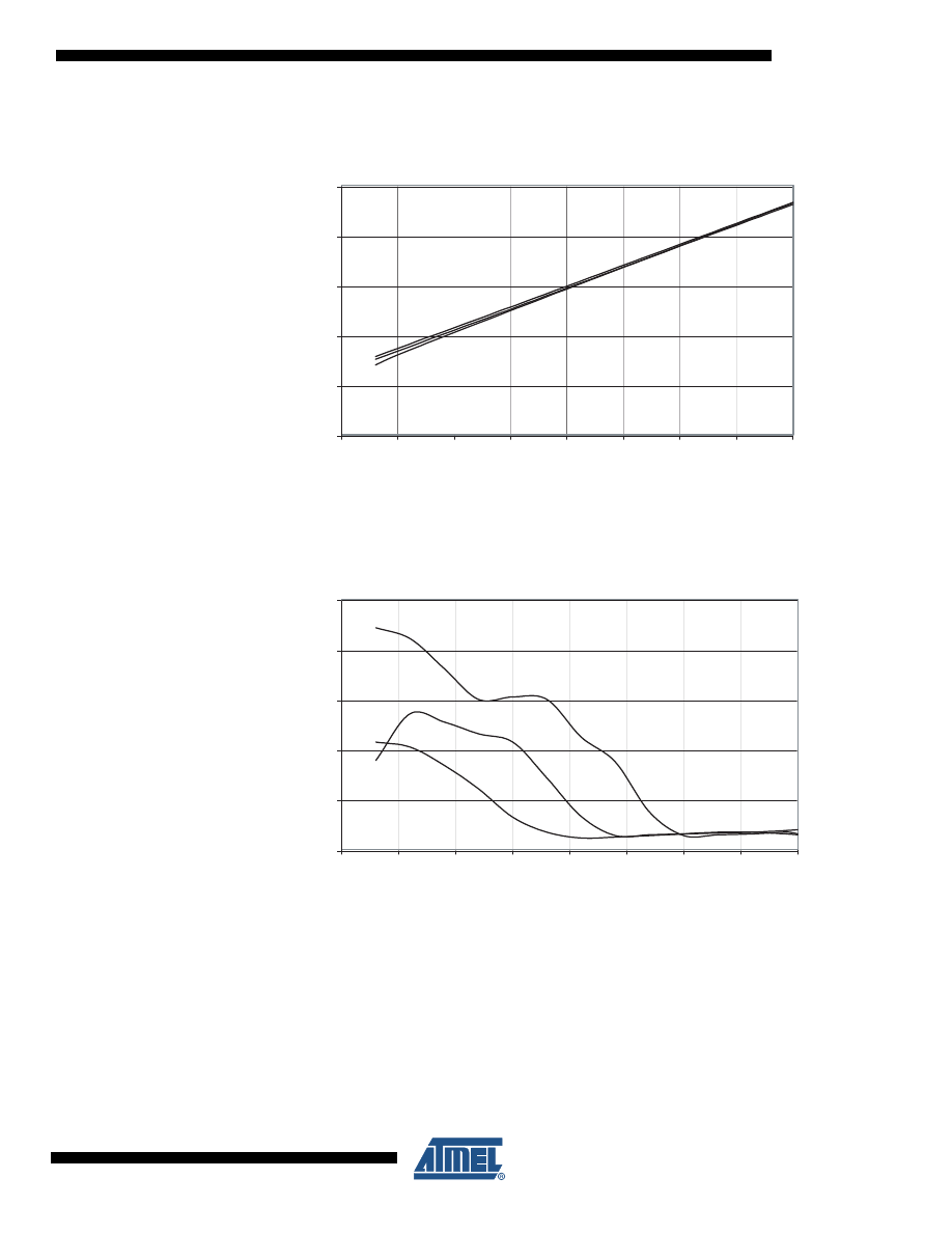
145
2535J–AVR–08/10
ATtiny13
Figure 19-44. Reset Input Threshold Voltage vs. V
CC
(VIL, Reset Pin Read as '0')
Figure 19-45. Reset Input Pin Hysteresis vs. V
CC
RESET INPUT THRESHOLD VOLTAGE vs. V
CC
VIL, IO PIN READ AS '0'
85 ˚C
25 ˚C
-40 ˚C
0
0.5
1
1.5
2
2.5
1.5
2
2.5
3
3.5
4
4.5
5
5.5
V
CC
(V)
Threshold (V)
RESET INPUT THRESHOLD VOLTAGE vs. V
CC
VIL, IO PIN READ AS '0'
0
0.1
0.2
0.3
0.4
0.5
1.5
2
2.5
3
3.5
4
4.5
5
5.5
V
CC
(V)
Threshold (V)
-40 ºC
25 ºC
85 ºC
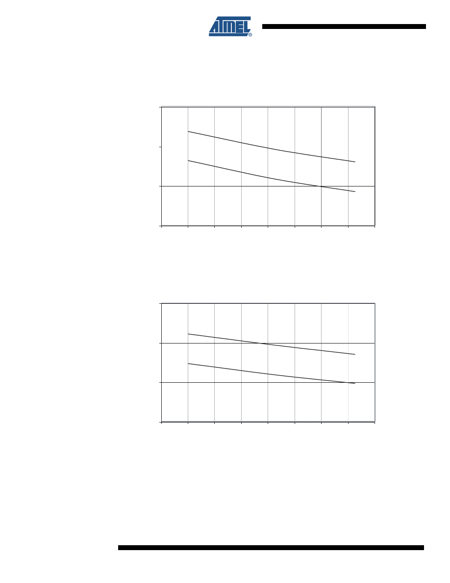
146
2535J–AVR–08/10
ATtiny13
19.7 BOD Thresholds and Analog Comparator Offset
Figure 19-46. BOD Thresholds vs. Temperature (BODLEVEL is 4.3V)
Figure 19-47. BOD Thresholds vs. Temperature (BODLEVEL is 2.7V)
BOD THRESHOLDS vs. TEMPERATURE
BODLEVEL IS 4.3
V
4.2
4.3
4.4
4.5
-60
-40
-20
0
20
40
60
80
100
Temperature (C)
Threshold (V)
Rising V
CC
Falling V
CC
BOD THRESHOLDS vs. TEMPERATURE
BODLEVEL IS 2.7
V
2.6
2.7
2.8
2.9
-60
-40
-20
0
20
40
60
80
100
Temperature (C)
Threshold (V)
Falling V
CC
Rising V
CC
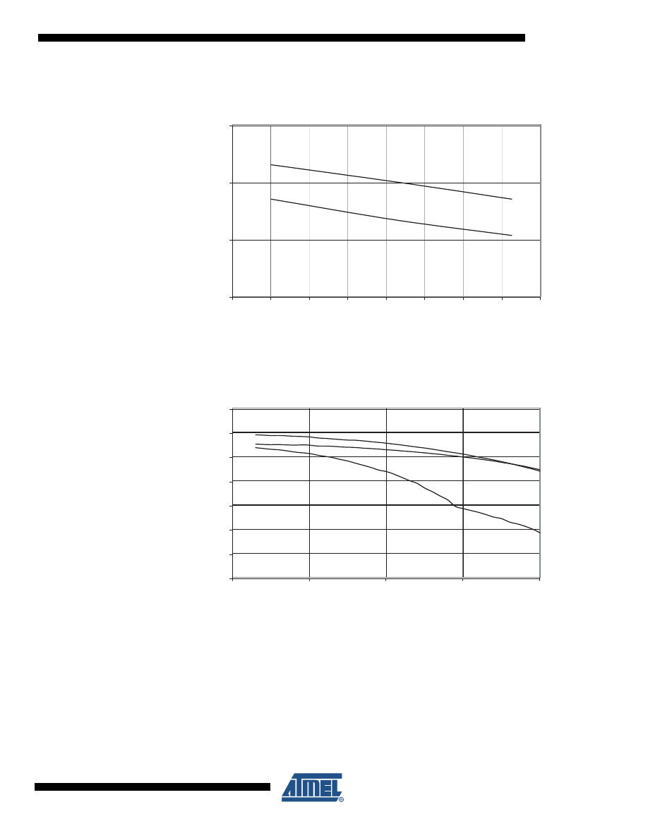
147
2535J–AVR–08/10
ATtiny13
Figure 19-48. BOD Thresholds vs. Temperature (BODLEVEL is 1.8V)
Figure 19-49. Bandgap Voltage vs. V
CC
BOD THRESHOLDS vs. TEMPERATURE
BODLEVEL IS 1.8
V
1.75
1.8
1.85
1.9
-60
-40
-20
0
20
40
60
80
100
Temperature (C)
Threshold (V)
Falling V
CC
Rising V
CC
BANDGAP VOLTAGE vs. V
CC
0.92
0.94
0.96
0.98
1
1.02
1.04
1.06
1.5
2.5
3.5
4.5
5.5
V
CC
(V)
Bandgap Voltage (V)
85ºC
25ºC
-40ºC

148
2535J–AVR–08/10
ATtiny13
19.8 Internal Oscillator Speed
Figure 19-50. Calibrated 9.6 MHz RC Oscillator Frequency vs. Temperature
Figure 19-51. Calibrated 9.6 MHz RC Oscillator Frequency vs. V
CC
CALIBRATED 9.6 MHz RC OSCILLATOR FREQUENCY vs. TEMPERATURE
5.5 V
4.5 V
2.7 V
1.8 V
8.5
8.7
8.9
9.1
9.3
9.5
9.7
9.9
10.1
10.3
-60
-40
-20
0
20
40
60
80
100
Temperature (C)
F
RC
(MHz)
CALIBRATED 9.6 MHz RC OSCILLATOR FREQUENCY vs. V
CC
85 ˚C
25 ˚C
-40 ˚C
8
8.5
9
9.5
10
10.5
11
1.5
2
2.5
3
3.5
4
4.5
5
5.5
V
CC
(V)
F
RC
(MHz)

149
2535J–AVR–08/10
ATtiny13
Figure 19-52. Calibrated 9.6 MHz RC Oscillator Frequency vs. Osccal Value
Figure 19-53. Calibrated 4.8 MHz RC Oscillator Frequency vs. Temperature
CALIBRATED 9.6MHz RC OSCILLATOR FREQUENCY vs. OSCCAL VALUE
25 ˚C
2
4
6
8
10
12
14
16
18
0
8
16
24
32
40
48
56
64
72
80
88
96
104
112
120
OSCCAL VALUE
F
RC
(MHz)
CALIBRATED 4.8 MHz RC OSCILLATOR FREQUENCY vs. TEMPERATURE
5.5 V
4.0 V
2.7 V
1.8 V
4.5
4.6
4.7
4.8
4.9
5
5.1
-60
-40
-20
0
20
40
60
80
100
Temperature (C)
F
RC
(MHz)
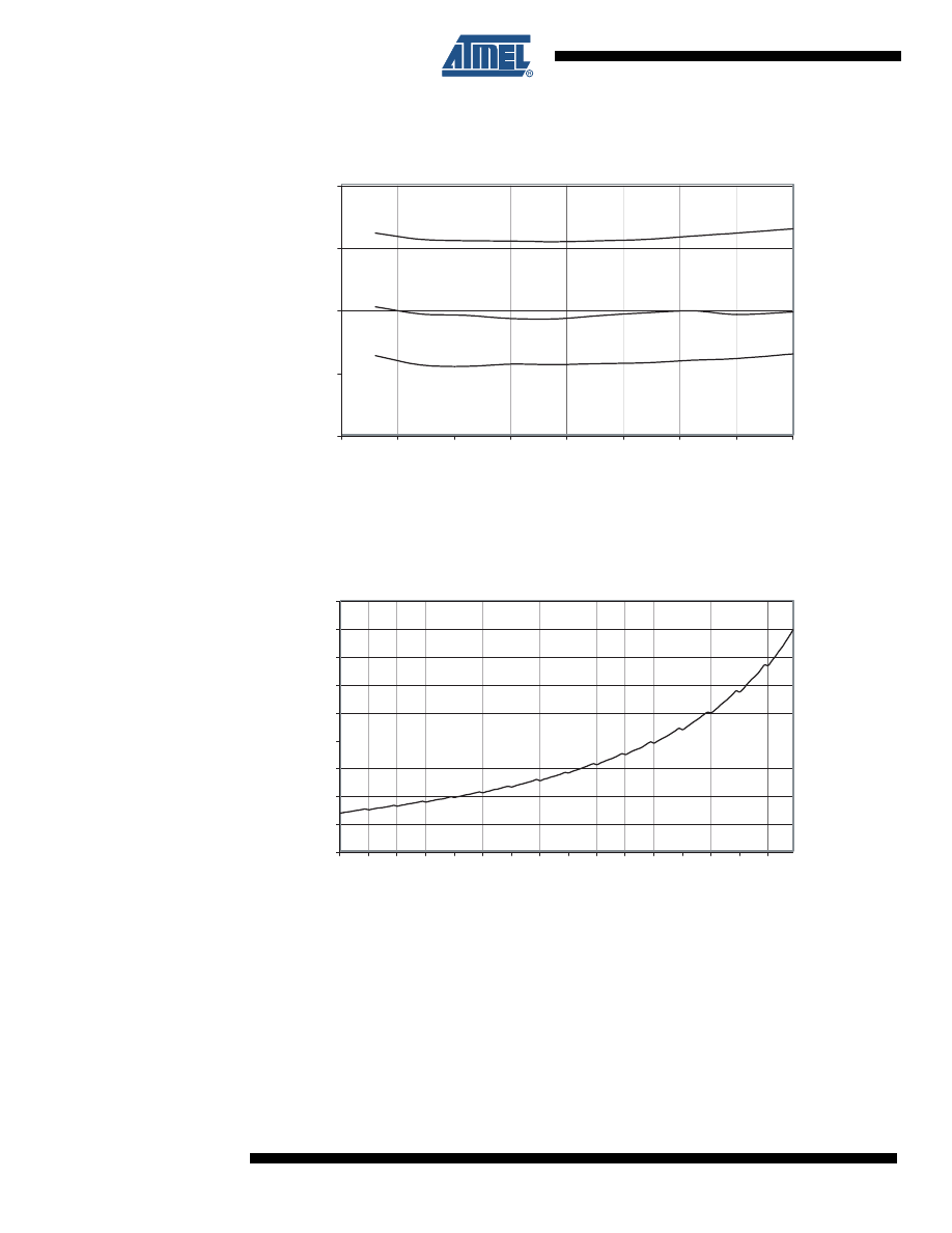
150
2535J–AVR–08/10
ATtiny13
Figure 19-54. Calibrated 4.8 MHz RC Oscillator Frequency vs. V
CC
Figure 19-55. Calibrated 4.8 MHz RC Oscillator Frequency vs. Osccal Value
CALIBRATED 4.8 MHz RC OSCILLATOR FREQUENCY vs. V
CC
85 ˚C
25 ˚C
-40 ˚C
4.4
4.6
4.8
5
5.2
1.5
2
2.5
3
3.5
4
4.5
5
5.5
V
CC
(V)
F
RC
(MHz)
CALIBRATED 4.8 MHz RC OSCILLATOR FREQUENCY vs. OSCCAL VALUE
25 ˚C
1
2
3
4
5
6
7
8
9
10
0
8
16
24
32
40
48
56
64
72
80
88
96
104
112
120 127
OSCCAL VALUE
F
RC
(MHz)
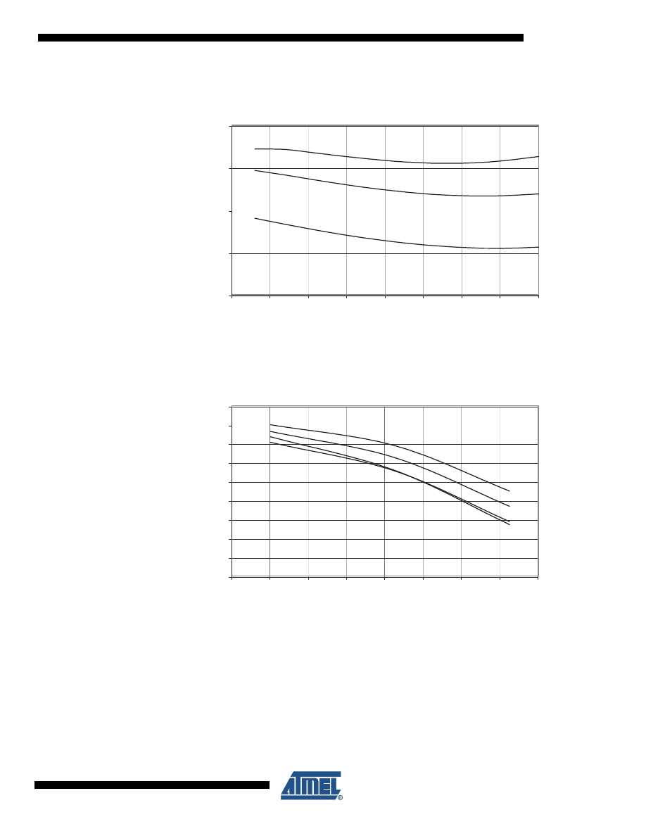
151
2535J–AVR–08/10
ATtiny13
Figure 19-56. 128 kHz Watchdog Oscillator Frequency vs. V
CC
Figure 19-57. 128 kHz Watchdog Oscillator Frequency vs. Temperature
128 kHz WATCHDOG OSCILLATOR FREQUENCY vs. V
CC
85 ˚C
25 ˚C
-40 ˚C
100
105
110
115
120
1.5
2
2.5
3
3.5
4
4.5
5
5.5
V
CC
(V)
F
RC
(kHz)
128 kHz WATCHDOG OSCILLATOR FREQUENCY vs. TEMPERATURE
5.5 V
4.0 V
2.7 V
1.8 V
100
102
104
106
108
110
112
114
116
118
-60
-40
-20
0
20
40
60
80
100
Temperature (C)
F
RC
(kHz)
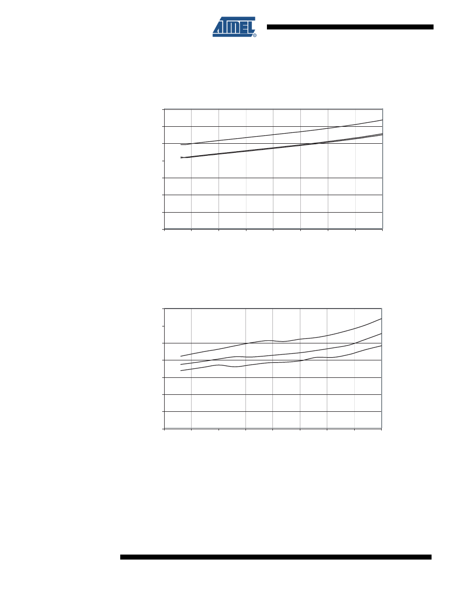
152
2535J–AVR–08/10
ATtiny13
19.9 Current Consumption of Peripheral Units
Figure 19-58. Brownout Detector Current vs. V
CC
Figure 19-59. ADC Current vs. V
CC
BROWNOUT DETECTOR CURRENT vs. V
CC
85 ˚C
25 ˚C
-40 ˚C
0
5
10
15
20
25
30
35
1.5
2
2.5
3
3.5
4
4.5
5
5.5
V
CC
(V)
I
CC
(uA)
ADC CURRENT vs. V
CC
85 ˚C
25 ˚C
-40 ˚C
0
50
100
150
200
250
300
350
1.5
2
2.5
3
3.5
4
4.5
5
5.5
V
CC
(V)
I
CC
(uA)
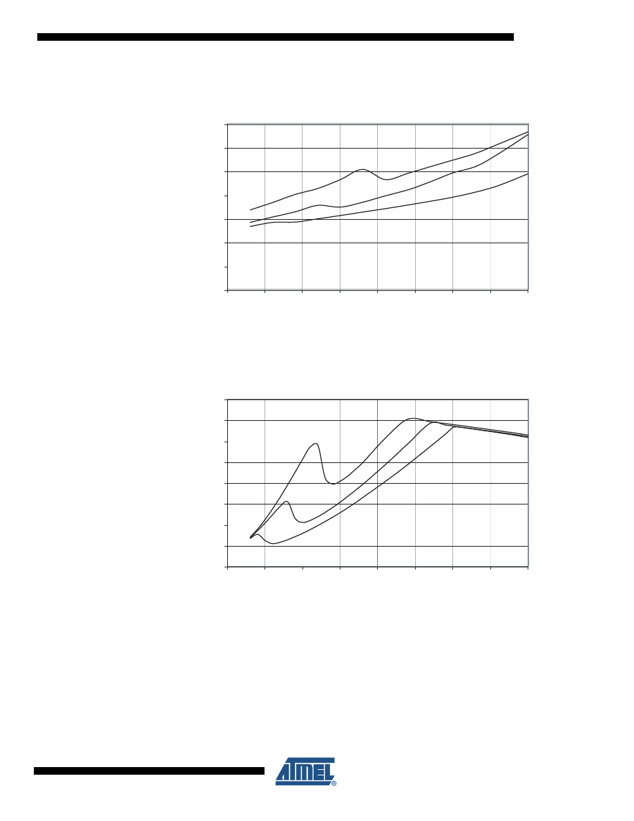
153
2535J–AVR–08/10
ATtiny13
Figure 19-60. Analog Comparator Current vs. V
CC
Figure 19-61. Programming Current vs. V
CC
ANALOG COMPARATOR CURRENT vs. V
CC
85 ˚C
25 ˚C
-40 ˚C
0
20
40
60
80
100
120
140
1.5
2
2.5
3
3.5
4
4.5
5
5.5
V
CC
(V)
I
CC
(uA)
PROGRAMMING CURRENT vs. Vcc
85 °C
25 °C
-40 °C
0
0.5
1
1.5
2
2.5
3
3.5
4
1.5
2
2.5
3
3.5
4
4.5
5
5.5
V
CC
(V)
I
CC
(mA)
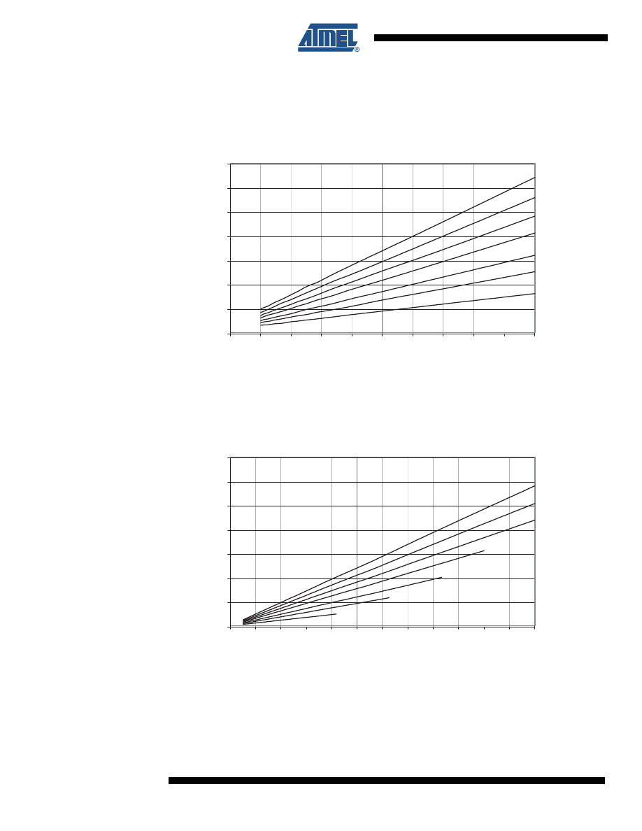
154
2535J–AVR–08/10
ATtiny13
19.10 Current Consumption in Reset and Reset Pulse width
Figure 19-62. Reset Supply Current vs. V
CC
(0.1 - 1.0 MHz, Excluding Current through the
Reset Pull-up)
Figure 19-63. Reset Supply Current vs. V
CC
(1 - 24 MHz, Excluding Current through the Reset
Pull-up)
RESET SUPPLY CURRENT vs. V
CC
0.1 - 1.0 MHz, EXCLUDING CURRENT THROUGH THE RESET PULL-UP
5.5 V
5.0 V
4.5 V
4.0 V
3.3 V
2.7 V
1.8 V
0
0.02
0.04
0.06
0.08
0.1
0.12
0.14
0
0.1
0.2
0.3
0.4
0.5
0.6
0.7
0.8
0.9
1
Frequency (MHz)
I
CC
(mA)
RESET SUPPLY CURRENT vs. V
CC
1 - 24 MHz, EXCLUDING CURRENT THROUGH THE RESET PULL-UP
0
0.5
1
1.5
2
2.5
3
3.5
0
2
4
6
8
10
12
14
16
18
20
22
24
Frequency (MHz)
I
CC
(mA)
2.7V
1.8V
4.0V
5.0V
4.5V
5.5V
3.3V
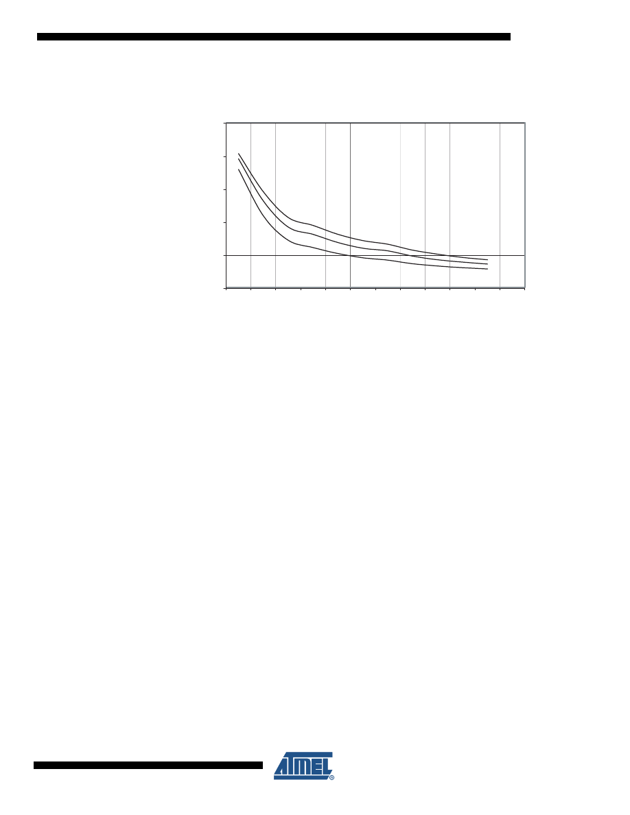
155
2535J–AVR–08/10
ATtiny13
Figure 19-64. Reset Pulse Width vs. V
CC
RESET PULSE WIDTH vs. V
CC
0
500
1000
1500
2000
2500
1.8
2.1
2.5
2.7
3
3.3
3.5
4
4.5
5
5.5
6
V
CC
(V)
Pulsewidth (ns)
85 ºC
25 ºC
-40 ºC
156
2535J–AVR–08/10
ATtiny13
20. Register Summary
Address
Name
Bit 7
Bit 6
Bit 5
Bit 4
Bit 3
Bit 2
Bit 1
Bit 0
Page
0x3F
SREG
I
T
H
S
V
N
Z
C
0x3E
Reserved
–
–
–
–
–
–
–
–
0x3D
SPL
SP[7:0]
0x3C
Reserved
–
0x3B
GIMSK
–
INT0
PCIE
–
–
–
–
–
0x3A GIFR
–
INTF0
PCIF
–
–
–
–
–
0x39 TIMSK0
–
–
–
–
OCIE0B
OCIE0A
TOIE0
–
0x38 TIFR0
–
–
–
–
OCF0B
OCF0A
TOV0
–
0x37 SPMCSR
–
–
–
CTPB
RFLB
PGWRT
PGERS
SELFPR-
0x36
OCR0A
Timer/Counter – Output Compare Register A
0x35
MCUCR
–
PUD
SE
SM1
SM0
–
ISC01
ISC00
0x34 MCUSR
–
–
–
–
WDRF
BORF
EXTRF
PORF
0x33 TCCR0B
FOC0A
FOC0B
–
–
WGM02
CS02
CS01
CS00
0x32 TCNT0
Timer/Counter
(8-bit)
0x31
OSCCAL
Oscillator Calibration Register
0x30 Reserved
–
0x2F
TCCR0A
COM0A1
COM0A0
COM0B1
COM0B0
–
–
WGM01
WGM00
0x2E
DWDR
DWDR[7:0]
0x2D
Reserved
–
0x2C
Reserved
–
0x2B
Reserved
–
0x2A Reserved
–
0x29
OCR0B
Timer/Counter – Output Compare Register B
0x28 GTCCR
TSM
–
–
–
–
–
–
PSR10
0x27 Reserved
–
0x26 CLKPR
CLKPCE
–
–
–
CLKPS3
CLKPS2
CLKPS1
CLKPS0
0x25
Reserved
–
0x24 Reserved
–
0x23 Reserved
–
0x22
Reserved
–
0x21 WDTCR
WDTIF
WDTIE
WDP3
WDCE
WDE
WDP2
WDP1
WDP0
0x20 Reserved
–
0x1F Reserved
–
0x1E
EEARL
–
–
EEPROM Address Register
0x1D
EEDR
EEPROM Data Register
0x1C
EECR
–
–
EEPM1
EEPM0
EERIE
EEMPE
EEPE
EERE
0x1B Reserved
–
0x1A
Reserved
–
0x19 Reserved
–
0x18 PORTB
–
–
PORTB5
PORTB4
PORTB3
PORTB2
PORTB1
PORTB0
0x17
DDRB
–
–
DDB5
DDB4
DDB3
DDB2
DDB1
DDB0
0x16 PINB
–
–
PINB5
PINB4
PINB3
PINB2
PINB1
PINB0
0x15
PCMSK
–
–
PCINT5
PCINT4
PCINT3
PCINT2
PCINT1
PCINT0
0x14 DIDR0
–
–
ADC0D
ADC2D
ADC3D
ADC1D
AIN1D
AIN0D
0x13 Reserved
–
0x12
Reserved
–
0x11 Reserved
–
0x10
Reserved
–
0x0F Reserved
–
0x0E Reserved
–
0x0D
Reserved
–
0x0C
Reserved
–
0x0B
Reserved
–
0x0A
Reserved
–
0x09
Reserved
–
0x08
ACSR
ACD
ACBG
ACO
ACI
ACIE
–
ACIS1
ACIS0
0x07
ADMUX
–
REFS0
ADLAR
–
–
–
MUX1
MUX0
0x06
ADCSRA
ADEN
ADSC
ADATE
ADIF
ADIE
ADPS2
ADPS1
ADPS0
0x05
ADCH
ADC Data Register High Byte
0x04
ADCL
ADC Data Register Low Byte
0x03
ADCSRB
–
ACME
–
–
–
ADTS2
ADTS1
ADTS0
0x02
Reserved
–
0x01
Reserved
–
0x00
Reserved
–

157
2535J–AVR–08/10
ATtiny13
Notes: 1. For compatibility with future devices, reserved bits should be written to zero if accessed. Reserved I/O memory addresses
should never be written.
2. I/O Registers within the address range 0x00 - 0x1F are directly bit-accessible using the SBI and CBI instructions. In these
registers, the value of single bits can be checked by using the SBIS and SBIC instructions.ome of the Status Flags are
cleared by writing a logical one to them. Note that, unlike most other AVRs, the CBI and SBI instructions will only operation
the specified bit, and can therefore be used on registers containing such Status Flags. The CBI and SBI instructions work
with registers 0x00 to 0x1F only.

158
2535J–AVR–08/10
ATtiny13
21. Instruction Set Summary
Mnemonics
Operands
Description
Operation
Flags
#Clocks
ARITHMETIC AND LOGIC INSTRUCTIONS
ADD
Rd, Rr
Add two Registers
Rd
← Rd + Rr
Z,C,N,V,H
1
ADC
Rd, Rr
Add with Carry two Registers
Rd
← Rd + Rr + C
Z,C,N,V,H
1
ADIW
Rdl,K
Add Immediate to Word
Rdh:Rdl
← Rdh:Rdl + K
Z,C,N,V,S
2
SUB
Rd, Rr
Subtract two Registers
Rd
← Rd - Rr
Z,C,N,V,H
1
SUBI
Rd, K
Subtract Constant from Register
Rd
← Rd - K
Z,C,N,V,H
1
SBC
Rd, Rr
Subtract with Carry two Registers
Rd
← Rd - Rr - C
Z,C,N,V,H
1
SBCI
Rd, K
Subtract with Carry Constant from Reg.
Rd
← Rd - K - C
Z,C,N,V,H
1
SBIW
Rdl,K
Subtract Immediate from Word
Rdh:Rdl
← Rdh:Rdl - K
Z,C,N,V,S
2
AND
Rd, Rr
Logical AND Registers
Rd
← Rd • Rr
Z,N,V
1
ANDI
Rd, K
Logical AND Register and Constant
Rd
← Rd • K
Z,N,V
1
OR
Rd, Rr
Logical OR Registers
Rd
← Rd v Rr
Z,N,V
1
ORI
Rd, K
Logical OR Register and Constant
Rd
← Rd v K
Z,N,V
1
EOR
Rd, Rr
Exclusive OR Registers
Rd
← Rd ⊕ Rr
Z,N,V
1
COM
Rd
One’s Complement
Rd
← 0xFF − Rd
Z,C,N,V
1
NEG
Rd
Two’s Complement
Rd
← 0x00 − Rd
Z,C,N,V,H
1
SBR
Rd,K
Set Bit(s) in Register
Rd
← Rd v K
Z,N,V
1
CBR
Rd,K
Clear Bit(s) in Register
Rd
← Rd • (0xFF - K)
Z,N,V
1
INC
Rd
Increment
Rd
← Rd + 1
Z,N,V
1
DEC
Rd
Decrement
Rd
← Rd − 1
Z,N,V
1
TST
Rd
Test for Zero or Minus
Rd
← Rd • Rd
Z,N,V
1
CLR
Rd
Clear Register
Rd
← Rd ⊕ Rd
Z,N,V
1
SER
Rd
Set Register
Rd
← 0xFF
None
1
BRANCH INSTRUCTIONS
RJMP
k
Relative Jump
PC
← PC + k + 1
None
2
IJMP
Indirect Jump to (Z)
PC
← Z
None
2
RCALL
k
Relative Subroutine Call
PC
← PC + k + 1
None
3
ICALL
Indirect Call to (Z)
PC
← Z
None
3
RET
Subroutine Return
PC
← STACK
None
4
RETI
Interrupt Return
PC
← STACK
I
4
CPSE
Rd,Rr
Compare, Skip if Equal
if (Rd = Rr) PC
← PC + 2 or 3
None
1/2/3
CP
Rd,Rr
Compare
Rd
− Rr
Z, N,V,C,H
1
CPC
Rd,Rr
Compare with Carry
Rd
− Rr − C
Z, N,V,C,H
1
CPI
Rd,K
Compare Register with Immediate
Rd
− K
Z, N,V,C,H
1
SBRC
Rr, b
Skip if Bit in Register Cleared
if (Rr(b)=0) PC
← PC + 2 or 3
None
1/2/3
SBRS
Rr, b
Skip if Bit in Register is Set
if (Rr(b)=1) PC
← PC + 2 or 3
None
1/2/3
SBIC
P, b
Skip if Bit in I/O Register Cleared
if (P(b)=0) PC
← PC + 2 or 3
None
1/2/3
SBIS
P, b
Skip if Bit in I/O Register is Set
if (P(b)=1) PC
← PC + 2 or 3
None
1/2/3
BRBS
s, k
Branch if Status Flag Set
if (SREG(s) = 1) then PC
←PC+k + 1
None
1/2
BRBC
s, k
Branch if Status Flag Cleared
if (SREG(s) = 0) then PC
←PC+k + 1
None
1/2
BREQ
k
Branch if Equal
if (Z = 1) then PC
← PC + k + 1
None
1/2
BRNE
k
Branch if Not Equal
if (Z = 0) then PC
← PC + k + 1
None
1/2
BRCS
k
Branch if Carry Set
if (C = 1) then PC
← PC + k + 1
None
1/2
BRCC
k
Branch if Carry Cleared
if (C = 0) then PC
← PC + k + 1
None
1/2
BRSH
k
Branch if Same or Higher
if (C = 0) then PC
← PC + k + 1
None
1/2
BRLO
k
Branch if Lower
if (C = 1) then PC
← PC + k + 1
None
1/2
BRMI
k
Branch if Minus
if (N = 1) then PC
← PC + k + 1
None
1/2
BRPL
k
Branch if Plus
if (N = 0) then PC
← PC + k + 1
None
1/2
BRGE
k
Branch if Greater or Equal, Signed
if (N
⊕ V= 0) then PC ← PC + k + 1
None
1/2
BRLT
k
Branch if Less Than Zero, Signed
if (N
⊕ V= 1) then PC ← PC + k + 1
None
1/2
BRHS
k
Branch if Half Carry Flag Set
if (H = 1) then PC
← PC + k + 1
None
1/2
BRHC
k
Branch if Half Carry Flag Cleared
if (H = 0) then PC
← PC + k + 1
None
1/2
BRTS
k
Branch if T Flag Set
if (T = 1) then PC
← PC + k + 1
None
1/2
BRTC
k
Branch if T Flag Cleared
if (T = 0) then PC
← PC + k + 1
None
1/2
BRVS
k
Branch if Overflow Flag is Set
if (V = 1) then PC
← PC + k + 1
None
1/2
BRVC
k
Branch if Overflow Flag is Cleared
if (V = 0) then PC
← PC + k + 1
None
1/2
BRIE
k
Branch if Interrupt Enabled
if ( I = 1) then PC
← PC + k + 1
None
1/2
BRID
k
Branch if Interrupt Disabled
if ( I = 0) then PC
← PC + k + 1
None
1/2
BIT AND BIT-TEST INSTRUCTIONS
SBI
P,b
Set Bit in I/O Register
I/O(P,b)
← 1
None
2
CBI
P,b
Clear Bit in I/O Register
I/O(P,b)
← 0
None
2
LSL
Rd
Logical Shift Left
Rd(n+1)
← Rd(n), Rd(0) ← 0
Z,C,N,V
1
LSR
Rd
Logical Shift Right
Rd(n)
← Rd(n+1), Rd(7) ← 0
Z,C,N,V
1
ROL
Rd
Rotate Left Through Carry
Rd(0)
←C,Rd(n+1)← Rd(n),C←Rd(7)
Z,C,N,V
1
159
2535J–AVR–08/10
ATtiny13
ROR
Rd
Rotate Right Through Carry
Rd(7)
←C,Rd(n)← Rd(n+1),C←Rd(0)
Z,C,N,V
1
ASR
Rd
Arithmetic Shift Right
Rd(n)
← Rd(n+1), n=0..6
Z,C,N,V
1
SWAP
Rd
Swap Nibbles
Rd(3..0)
←Rd(7..4),Rd(7..4)←Rd(3..0)
None
1
BSET
s
Flag Set
SREG(s)
← 1
SREG(s)
1
BCLR
s
Flag Clear
SREG(s)
← 0
SREG(s)
1
BST
Rr, b
Bit Store from Register to T
T
← Rr(b)
T
1
BLD
Rd, b
Bit load from T to Register
Rd(b)
← T
None
1
SEC
Set Carry
C
← 1
C
1
CLC
Clear Carry
C
← 0
C
1
SEN
Set Negative Flag
N
← 1
N
1
CLN
Clear Negative Flag
N
← 0
N
1
SEZ
Set Zero Flag
Z
← 1
Z
1
CLZ
Clear Zero Flag
Z
← 0
Z
1
SEI
Global Interrupt Enable
I
← 1
I
1
CLI
Global Interrupt Disable
I
← 0
I
1
SES
Set Signed Test Flag
S
← 1
S
1
CLS
Clear Signed Test Flag
S
← 0
S
1
SEV
Set Twos Complement Overflow.
V
← 1
V
1
CLV
Clear Twos Complement Overflow
V
← 0
V
1
SET
Set T in SREG
T
← 1
T
1
CLT
Clear T in SREG
T
← 0
T
1
SEH
Set Half Carry Flag in SREG
H
← 1
H
1
CLH
Clear Half Carry Flag in SREG
H
← 0
H
1
DATA TRANSFER INSTRUCTIONS
MOV
Rd, Rr
Move Between Registers
Rd
← Rr
None
1
MOVW
Rd, Rr
Copy Register Word
Rd+1:Rd
← Rr+1:Rr
None
1
LDI
Rd, K
Load Immediate
Rd
← K
None
1
LD
Rd, X
Load Indirect
Rd
← (X)
None
2
LD
Rd, X+
Load Indirect and Post-Inc.
Rd
← (X), X ← X + 1
None
2
LD
Rd, - X
Load Indirect and Pre-Dec.
X
← X - 1, Rd ← (X)
None
2
LD
Rd, Y
Load Indirect
Rd
← (Y)
None
2
LD
Rd, Y+
Load Indirect and Post-Inc.
Rd
← (Y), Y ← Y + 1
None
2
LD
Rd, - Y
Load Indirect and Pre-Dec.
Y
← Y - 1, Rd ← (Y)
None
2
LDD
Rd,Y+q
Load Indirect with Displacement
Rd
← (Y + q)
None
2
LD
Rd, Z
Load Indirect
Rd
← (Z)
None
2
LD
Rd, Z+
Load Indirect and Post-Inc.
Rd
← (Z), Z ← Z+1
None
2
LD
Rd, -Z
Load Indirect and Pre-Dec.
Z
← Z - 1, Rd ← (Z)
None
2
LDD
Rd, Z+q
Load Indirect with Displacement
Rd
← (Z + q)
None
2
LDS
Rd, k
Load Direct from SRAM
Rd
← (k)
None
2
ST
X, Rr
Store Indirect
(X)
← Rr
None
2
ST
X+, Rr
Store Indirect and Post-Inc.
(X)
← Rr, X ← X + 1
None
2
ST
- X, Rr
Store Indirect and Pre-Dec.
X
← X - 1, (X) ← Rr
None
2
ST
Y, Rr
Store Indirect
(Y)
← Rr
None
2
ST
Y+, Rr
Store Indirect and Post-Inc.
(Y)
← Rr, Y ← Y + 1
None
2
ST
- Y, Rr
Store Indirect and Pre-Dec.
Y
← Y - 1, (Y) ← Rr
None
2
STD
Y+q,Rr
Store Indirect with Displacement
(Y + q)
← Rr
None
2
ST
Z, Rr
Store Indirect
(Z)
← Rr
None
2
ST
Z+, Rr
Store Indirect and Post-Inc.
(Z)
← Rr, Z ← Z + 1
None
2
ST
-Z, Rr
Store Indirect and Pre-Dec.
Z
← Z - 1, (Z) ← Rr
None
2
STD
Z+q,Rr
Store Indirect with Displacement
(Z + q)
← Rr
None
2
STS
k, Rr
Store Direct to SRAM
(k)
← Rr
None
2
LPM
Load Program Memory
R0
← (Z)
None
3
LPM
Rd, Z
Load Program Memory
Rd
← (Z)
None
3
LPM
Rd, Z+
Load Program Memory and Post-Inc
Rd
← (Z), Z ← Z+1
None
3
SPM
Store Program Memory
(z)
← R1:R0
None
IN
Rd, P
In Port
Rd
← P
None
1
OUT
P, Rr
Out Port
P
← Rr
None
1
PUSH
Rr
Push Register on Stack
STACK
← Rr
None
2
POP
Rd
Pop Register from Stack
Rd
← STACK
None
2
MCU CONTROL INSTRUCTIONS
NOP
No Operation
None
1
SLEEP
Sleep
(see specific descr. for Sleep function)
None
1
WDR
Watchdog Reset
(see specific descr. for WDR/Timer)
None
1
BREAK
Break
For On-chip Debug Only
None
N/A
Mnemonics
Operands
Description
Operation
Flags
#Clocks

160
2535J–AVR–08/10
ATtiny13
22. Ordering Information
Notes: 1. These devices can also be supplied in wafer form. Please contact your local Atmel sales office for detailed ordering informa-
tion and minimum quantities.
2. All packages are Pb-free, halide-free and fully green and they comply with the European directive for Restriction of Hazard-
ous Substances (RoHS).
3. For Speed vs. V
CC
4. Code indicators:
– U: matte tin
– R: tape & reel
Speed (MHz)
Power Supply (V)
Operation Range
10
1.8 - 5.5
ATtiny13V-10PU
ATtiny13V-10SU
ATtiny13V-10SUR
ATtiny13V-10SSU
ATtiny13V-10SSUR
ATtiny13V-10MU
ATtiny13V-10MUR
ATtiny13V-10MMU
ATtiny13V-10MMUR
8P3
8S2
8S2
S8S1
S8S1
20M1
20M1
10M1
10M1
Industrial
(-40
°C to +85°C)
20
2.7 - 5.5
ATtiny13-20PU
ATtiny13-20SU
ATtiny13-20SUR
ATtiny13-20SSU
ATtiny13-20SSUR
ATtiny13-20MU
ATtiny13-20MUR
ATtiny13-20MMU
ATtiny13-20MMUR
8P3
8S2
8S2
S8S1
S8S1
20M1
20M1
10M1
10M1
Industrial
(-40
°C to +85°C)
Package Type
8P3
8-lead, 0.300" Wide, Plastic Dual Inline Package (PDIP)
8S2
8-lead, 0.209" Wide, Plastic Small Outline Package (EIAJ SOIC)
S8S1
8-lead, 0.150" Wide, Plastic Gull-Wing Small Outline (JEDEC SOIC)
20M1
20-pad, 4 x 4 x 0.8 mm Body, Lead Pitch 0.50 mm, Micro Lead Frame Package (MLF)
10M1
10-pad, 3 x 3 x 1 mm Body, Lead Pitch 0.50 mm, Micro Lead Frame Package (MLF)
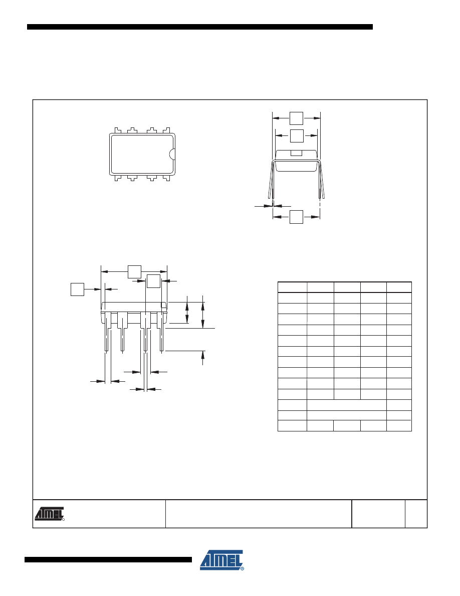
161
2535J–AVR–08/10
ATtiny13
23. Packaging Information
23.1 8P3
2325 Orchard Parkway
San Jose, CA 95131
TITLE
DRAWING NO.
R
REV.
8P3, 8-lead, 0.300" Wide Body, Plastic Dual
In-line Package (PDIP)
01/09/02
8P3
B
D
D1
E
E1
e
L
b2
b
A2 A
1
N
eA
c
b3
4 PLCS
Top View
Side View
End View
COMMON DIMENSIONS
(Unit of Measure = inches)
SYMBOL
MIN
NOM
MAX
NOTE
Notes:
1. This drawing is for general information only; refer to JEDEC Drawing MS-001, Variation BA for additional information.
2. Dimensions A and L are measured with the package seated in JEDEC seating plane Gauge GS-3.
3. D, D1 and E1 dimensions do not include mold Flash or protrusions. Mold Flash or protrusions shall not exceed 0.010 inch.
4. E and eA measured with the leads constrained to be perpendicular to datum.
5. Pointed or rounded lead tips are preferred to ease insertion.
6. b2 and b3 maximum dimensions do not include Dambar protrusions. Dambar protrusions shall not exceed 0.010 (0.25 mm).
A
0.210
2
A2
0.115
0.130
0.195
b
0.014
0.018
0.022
5
b2
0.045
0.060
0.070
6
b3
0.030
0.039
0.045
6
c
0.008
0.010
0.014
D
0.355
0.365
0.400
3
D1
0.005
3
E
0.300
0.310
0.325
4
E1
0.240
0.250
0.280
3
e
0.100 BSC
eA
0.300 BSC
4
L
0.115
0.130
0.150
2
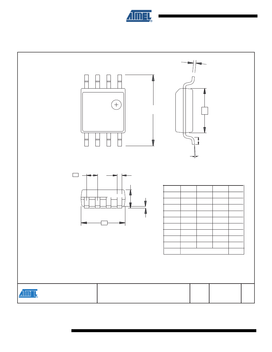
162
2535J–AVR–08/10
ATtiny13
23.2 8S2
TITLE
DRAWING NO.
GPC
REV.
Package Drawing Contact:
packagedrawings@atmel.com
8S2
STN
F
8S2, 8-lead, 0.208” Body, Plastic Small
Outline Package (EIAJ)
4/15/08
COMMON DIMENSIONS
(Unit of Measure = mm)
SYMBOL
MIN
NOM
MAX
NOTE
Notes: 1. This drawing is for general information only; refer to EIAJ Drawing EDR-7320 for additional information.
2. Mismatch of the upper and lower dies and resin burrs aren't included.
3. Determines the true geometric position.
4. Values b,C apply to plated terminal. The standard thickness of the plating layer shall measure between 0.007 to .021 mm.
A 1.70
2.16
A1 0.05
0.25
b
0.35
0.48
4
C
0.15
0.35
4
D 5.13
5.35
E1 5.18
5.40
2
E 7.70
8.26
L 0.51
0.85
θ
0°
8°
e
1.27 BSC
3
θθ
1
1
N
N
E
E
TOP VIEW
TOP VIEW
C
C
E1
E1
END VIEW
END VIEW
A
A
b
b
L
L
A1
A1
e
e
D
D
SIDE VIEW
SIDE VIEW
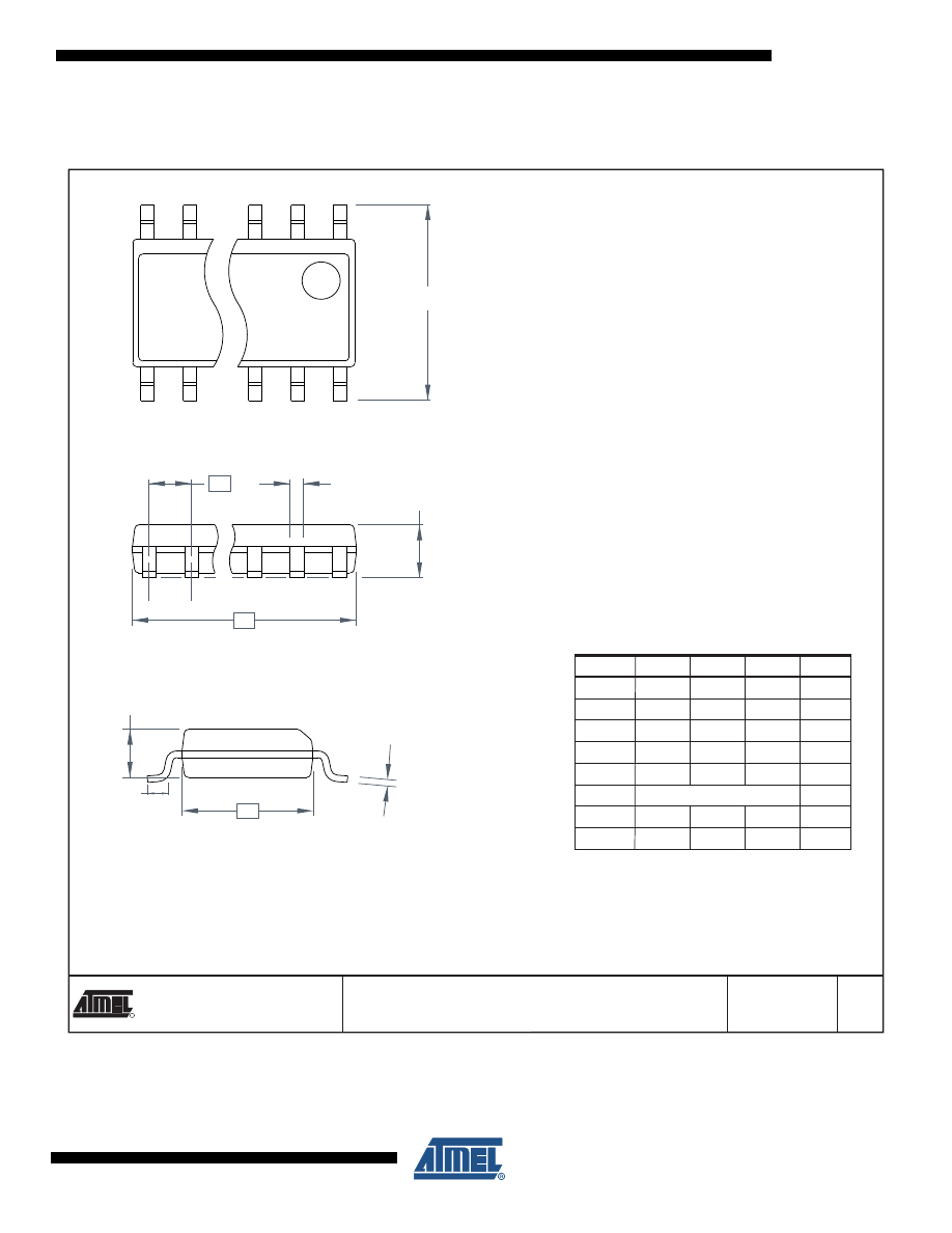
163
2535J–AVR–08/10
ATtiny13
23.3 S8S1
2325 Orchard Parkway
San Jose, CA 95131
TITLE
DRAWING NO.
R
REV.
Note:
10/10/01
8S1, 8-lead (0.150" Wide Body), Plastic Gull Wing
Small Outline (JEDEC SOIC)
8S1
A
H
1
2
N
3
Top View
C
E
End View
A
B
L
A2
e
D
Side View
COMMON DIMENSIONS
(Unit of Measure = mm)
SYMBOL
MIN
NOM
MAX
NOTE
This drawing is for general information only. Refer to JEDEC Drawing MS-012 for proper dimensions, tolerances, datums, etc.
A
–
–
1.75
B
–
–
0.51
C
–
–
0.25
D
–
–
5.00
E
–
–
4.00
e
1.27 BSC
H
–
–
6.20
L
–
–
1.27
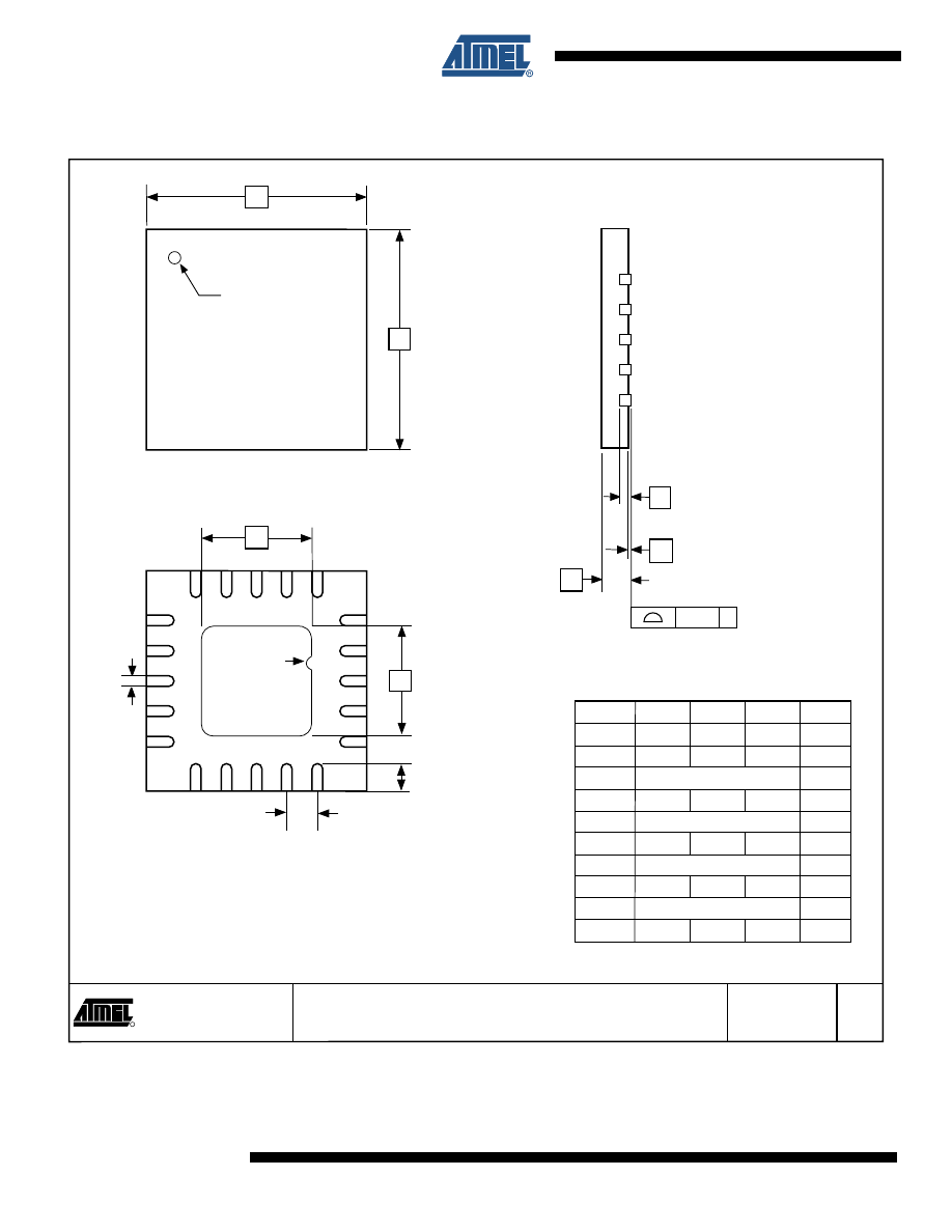
164
2535J–AVR–08/10
ATtiny13
23.4 20M1
2325 Orchard Parkway
San Jose, CA 95131
TITLE
DRAWING NO.
R
REV.
20M1, 20-pad, 4 x 4 x 0.8 mm Body, Lead Pitch 0.50 mm,
A
20M1
10/27/04
2.6 mm Exposed Pad, Micro Lead Frame Package (MLF)
A 0.70
0.75
0.80
A1 – 0.01
0.05
A2
0.20
REF
b 0.18
0.23
0.30
D
4.00
BSC
D2 2.45 2.60 2.75
E
4.00
BSC
E2 2.45 2.60 2.75
e
0.50 BSC
L 0.35
0.40
0.55
SIDE VIEW
Pin 1 ID
Pin #1
Notch
(0.20 R)
BOTTOM VIEW
TOP VIEW
Note: Reference JEDEC Standard MO-220, Fig. 1 (SAW Singulation) WGGD-5.
COMMON DIMENSIONS
(Unit of Measure = mm)
SYMBOL
MIN
NOM
MAX
NOTE
D
E
e
A2
A1
A
D2
E2
0.08
C
L
1
2
3
b
1
2
3
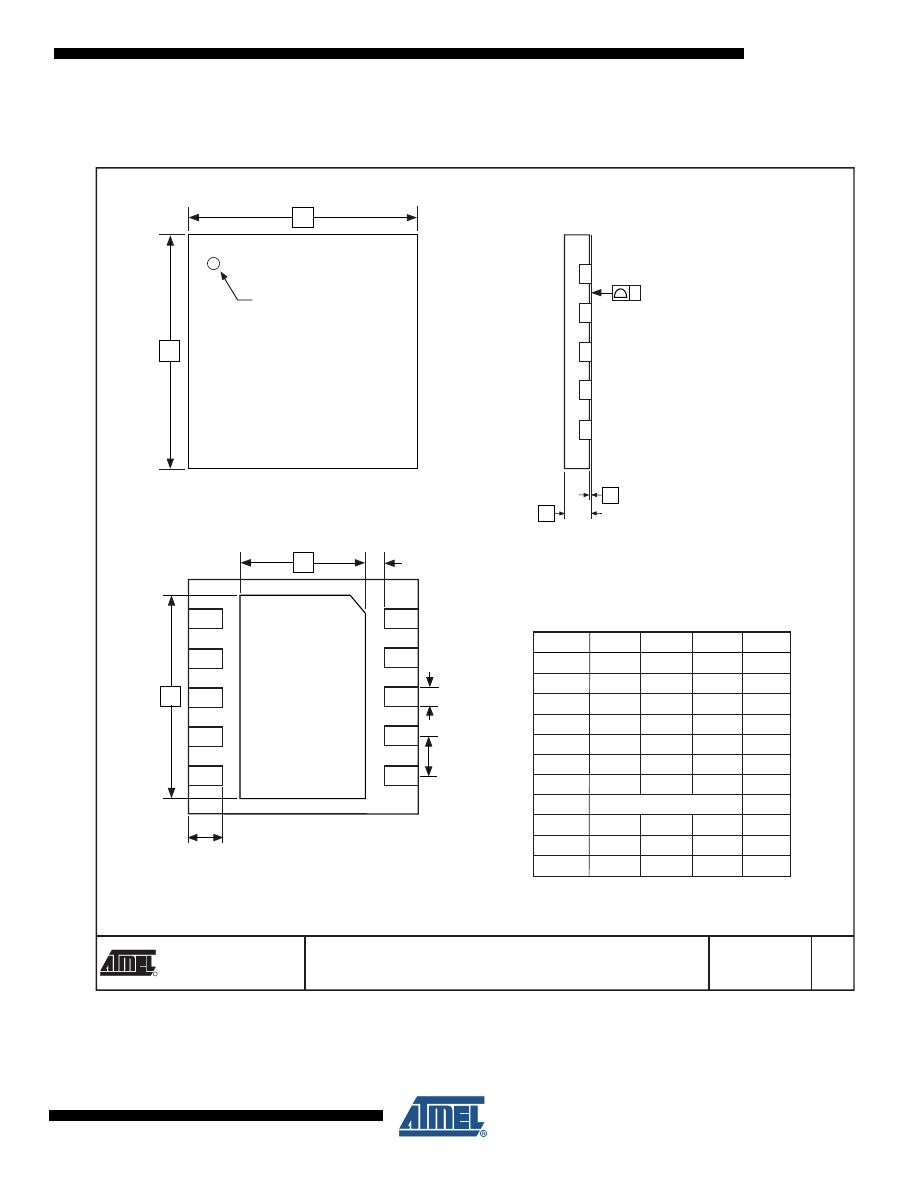
165
2535J–AVR–08/10
ATtiny13
23.5 10M1
2325 Orchard Parkway
San Jose, CA 95131
TITLE
DRAWING NO.
R
REV.
10M1, 10-pad, 3 x 3 x 1.0 mm Body, Lead Pitch 0.50 mm,
1.64 x 2.60 mm Exposed Pad, Micro Lead Frame Package
A
10M1
7/7/06
COMMON DIMENSIONS
(Unit of Measure = mm)
SYMBOL
MIN
NOM
MAX
NOTE
A
0.80 0.90 1.00
A1
0.00 0.02 0.05
b
0.18
0.25
0.30
D
2.90
3.00
3.10
D1
1.40
–
1.75
E
2.90
3.00
3.10
E1
2.20
–
2.70
e
0.50
L
0.30
–
0.50
y
– –
0.08
K
0.20
–
–
Pin 1 ID
TOP VIEW
D
E
A1
A
SIDE VIEW
BOTTOM VIEW
D1
E1
L
b
e
K
1
2
Notes: 1. This package conforms to JEDEC reference MO-229C, Variation VEED-5.
2. The terminal #1 ID is a Lasser-marked Feature.
y

166
2535J–AVR–08/10
ATtiny13
24. Errata
The revision letter in this section refers to the revision of the ATtiny13 device.
24.1 ATtiny13 Rev. D
•
EEPROM can not be written below 1.9 Volt
1. EEPROM can not be written below 1.9 Volt
Writing the EEPROM at V
CC
below 1.9 volts might fail.
Problem Fix/Workaround
Do not write the EEPROM when V
CC
is below 1.9 volts.
24.2 ATtiny13 Rev. C
Revision C has not been sampled.
24.3 ATtiny13 Rev. B
•
Wrong values read after Erase Only operation
•
High Voltage Serial Programming Flash, EEPROM, Fuse and Lock Bits may fail
•
Device may lock for further programming
•
debugWIRE communication not blocked by lock-bits
•
Watchdog Timer Interrupt disabled
•
EEPROM can not be written below 1.9 Volt
24.3.1
Wrong values read after Erase Only operation
At supply voltages below 2.7 V, an EEPROM location that is erased by the Erase Only oper-
ation may read as programmed (0x00).
Problem Fix/Workaround
If it is necessary to read an EEPROM location after Erase Only, use an Atomic Write opera-
tion with 0xFF as data in order to erase a location. In any case, the Write Only operation can
be used as intended. Thus no special considerations are needed as long as the erased loca-
tion is not read before it is programmed.
24.3.2
High Voltage Serial Programming Flash, EEPROM, Fuse and Lock Bits may fail
Writing to any of these locations and bits may in some occasions fail.
Problem Fix/Workaround
After a writing has been initiated, always observe the RDY/BSY signal. If the writing should
fail, rewrite until the RDY/BSY verifies a correct writing. This will be fixed in revision D.
24.3.3
Device may lock for further programming
Special combinations of fuse bits will lock the device for further programming effectively
turning it into an OTP device. The following combinations of settings/fuse bits will cause this
effect:
– 128 kHz internal oscillator (CKSEL[1..0] = 11), shortest start-up time
(SUT[1..0] = 00), Debugwire enabled (DWEN = 0) or Reset disabled RSTDISBL = 0.
– 9.6 MHz internal oscillator (CKSEL[1..0] = 10), shortest start-up time
(SUT[1..0] = 00), Debugwire enabled (DWEN = 0) or Reset disabled RSTDISBL = 0.

167
2535J–AVR–08/10
ATtiny13
– 4.8 MHz internal oscillator (CKSEL[1..0] = 01), shortest start-up time
(SUT[1..0] = 00), Debugwire enabled (DWEN = 0) or Reset disabled RSTDISBL = 0.
Problem fix/ Workaround
Avoid the above fuse combinations. Selecting longer start-up time will eliminate the problem.
24.3.4
debugWIRE communication not blocked by lock-bits
When debugWIRE on-chip debug is enabled (DWEN = 0), the contents of program memory
and EEPROM data memory can be read even if the lock-bits are set to block further reading
of the device.
Problem fix/ Workaround
Do not ship products with on-chip debug of the tiny13 enabled.
24.3.5
Watchdog Timer Interrupt disabled
If the watchdog timer interrupt flag is not cleared before a new timeout occurs, the watchdog
will be disabled, and the interrupt flag will automatically be cleared. This is only applicable in
interrupt only mode. If the Watchdog is configured to reset the device in the watchdog time-
out following an interrupt, the device works correctly.
Problem fix / Workaround
Make sure there is enough time to always service the first timeout event before a new
watchdog timeout occurs. This is done by selecting a long enough time-out period.
24.3.6
EEPROM can not be written below 1.9 Volt
Writing the EEPROM at V
CC
below 1.9 volts might fail.
Problem Fix/Workaround
Do not write the EEPROM when V
CC
is below 1.9 volts.
24.4 ATtiny13 Rev. A
Revision A has not been sampled.

168
2535J–AVR–08/10
ATtiny13
25. Datasheet Revision History
Please note that the referring page numbers in this section refer to the complete document.
25.1 Rev. 2535J-08/10
Added tape and reel part numbers in
“Ordering Information” on page 160
. Removed text “Not
recommended for new design” from cover page. Updated last page.
25.2 Rev. 2535I-05/08
1. Updated document template, layout and paragraph formats.
2. Updated
.
3. Created Sections:
–
“Calibrated Internal RC Oscillator Accuracy” on page 118
–
“Analog Comparator Characteristics” on page 119
4. Updated Sections:
–
“System Clock and Clock Options” on page 23
–
“Calibrated Internal 4.8/9.6 MHz Oscillator” on page 25
–
“External Interrupts” on page 45
–
“Analog Noise Canceling Techniques” on page 88
–
“Limitations of debugWIRE” on page 96
–
“Reading Fuse and Lock Bits from Firmware” on page 99
–
–
“Calibration Bytes” on page 104
–
“High-Voltage Serial Programming” on page 108
–
“Ordering Information” on page 160
5. Updated Figure:
–
“Analog Input Circuitry” on page 87
–
“High-voltage Serial Programming Timing” on page 122
6. Moved Figures:
–
“Serial Programming Timing” on page 121
–
“Serial Programming Waveform” on page 121
–
“High-voltage Serial Programming Timing” on page 122
7. Updated Tables:
–
“DC Characteristics, TA = -40°C to +85°C” on page 115
–
8. Moved Tables:
–
“Serial Programming Instruction Set” on page 107
–
–
9. Updated Register Description for Sections:

169
2535J–AVR–08/10
ATtiny13
–
“TCCR0A – Timer/Counter Control Register A” on page 69
–
“DIDR0 – Digital Input Disable Register 0” on page 94
10. Updated description in
11. Changed device status to “Not Recommended for New Designs”.
25.3 Rev. 2535H-10/07
25.4 Rev. 2535G-01/07
25.5 Rev. 2535F-04/06
25.6 Rev. 2535E-10/04
1.
Updated
2.
Updated
“Pin Configurations” on page 2
.
3.
Added
.
4.
Updated
“Assembly Code Example(1)” on page 39
5.
“Alternate Functions of Port B” on page 54
.
6.
Updated Bit 5 description in
“GIMSK – General Interrupt Mask Register” on page 46
.
7.
Updated
“ADC Voltage Reference” on page 87
.
8.
Updated
“Calibration Bytes” on page 104
9.
Updated
“Read Calibration Byte” on page 108
.
10.
Updated Table 51 in
“Serial Programming Characteristics” on page 121
11.
Updated Algorithm in
“High-Voltage Serial Programming Algorithm” on page 109
12.
Updated
“Read Calibration Byte” on page 112
.
13.
Updated values in
“External Clock Drive” on page 118
14.
Updated
“Ordering Information” on page 160
15.
Updated
“Packaging Information” on page 161
1.
Removed Preliminary.
2.
Updated
,
,
3.
4.
Updated
“Bit 6 – ACBG: Analog Comparator Bandgap Select” on page 79
5.
Updated
“Prescaling and Conversion Timing” on page 83
.
6.
Updated
.
7.
Updated
“DC Characteristics” on page 115
.
8.
Updated
“Ordering Information” on page 160
9.
Updated
“Packaging Information” on page 161
1.
Revision not published.
1.
Bits EEMWE/EEWE changed to EEMPE/EEPE in document.
2.
Updated
“Pinout ATtiny13/ATtiny13V” on page 2
.
3.
Updated “Write Fuse Low Bits” in
.
2.
Added
“Pin Change Interrupt Timing” on page 45
.
4.
Updated
“GIMSK – General Interrupt Mask Register” on page 46
.
5.
Updated
“PCMSK – Pin Change Mask Register” on page 47
.
6.
Updated item 4 in
“Serial Programming Algorithm” on page 106
.
7.
Updated
“High-Voltage Serial Programming Algorithm” on page 109
.

170
2535J–AVR–08/10
ATtiny13
25.7 Rev. 2535D-04/04
25.8 Rev. 2535C-02/04
25.9 Rev. 2535B-01/04
25.10 Rev. 2535A-06/03
8.
Updated
“DC Characteristics” on page 115
.
9.
Updated
“Typical Characteristics” on page 122
.
10.
Updated
“Ordering Information” on page 160
11.
Updated
“Packaging Information” on page 161
12.
Updated
.
1.
Maximum Speed Grades changed: 12MHz to 10MHz, 24MHz to 20MHz
2.
Updated
“Serial Programming Instruction Set” on page 107
3.
Updated
4.
Updated
“Ordering Information” on page 160
1.
C-code examples updated to use legal IAR syntax.
2.
Replaced occurrences of WDIF with WDTIF and WDIE with WDTIE.
3.
Updated
.
4.
Updated
“Calibrated Internal 4.8/9.6 MHz Oscillator” on page 25
.
5.
Updated
“OSCCAL – Oscillator Calibration Register” on page 27
6.
Updated typo in introduction on
7.
Updated
“ADC Conversion Time” on page 86
.
8.
Updated
“Serial Programming” on page 105
9.
Updated
“Electrical Characteristics” on page 115
10.
Updated
“Ordering Information” on page 160
11.
Removed rev. C from
.
1.
Updated
.
2.
Updated
,
and
3.
Updated
“Calibrated Internal 4.8/9.6 MHz Oscillator” on page 25
.
4.
.
5.
Updated
and
6.
Updated registers “MCUCR – MCU Control Register”, “TCCR0B – Timer/Counter Con-
trol Register B” and “DIDR0 – Digital Input Disable Register 0”.
7.
Updated Absolute Maximum Ratings and DC Characteristics in
.
8.
Added
9.
Updated
.
10.
Updated
“Typical Characteristics” on page 123
.
11.
Updated
“Ordering Information” on page 160
12.
Updated
“Packaging Information” on page 161
13.
Updated
.
14.
Changed instances of EEAR to EEARL.
1.
Initial Revision.

i
2535J–AVR–08/10
ATtiny13
Table of Contents
4
CPU Core .................................................................................................. 7
In-System Reprogrammable Flash Program Memory .....................................15
System Clock and Clock Options ......................................................... 23
Power Management and Sleep Modes ................................................. 30
7.2

ii
2535J–AVR–08/10
ATtiny13
System Control and Reset .................................................................... 34
11 8-bit Timer/Counter0 with PWM ............................................................ 58
Analog Comparator Multiplexed Input .............................................................78
14 Analog to Digital Converter .................................................................. 81

iii
2535J–AVR–08/10
ATtiny13
Changing Channel or Reference Selection .....................................................86
Analog Noise Canceling Techniques ...............................................................88
15 debugWIRE On-chip Debug System .................................................... 95
16 Self-Programming the Flash ................................................................. 97
Filling the Temporary Buffer (Page Loading) ...................................................97
Addressing the Flash During Self-Programming .............................................98
EEPROM Write Prevents Writing to SPMCSR ................................................99
Reading Fuse and Lock Bits from Firmware ...................................................99
Programming Time for Flash when Using SPM ............................................100
17 Memory Programming ......................................................................... 102
Program And Data Memory Lock Bits ...........................................................102
17.5

iv
2535J–AVR–08/10
ATtiny13
High-Voltage Serial Programming .................................................................108
Considerations for Efficient Programming .....................................................112
System and Reset Characteristics ................................................................119
Analog Comparator Characteristics ...............................................................119
Serial Programming Characteristics ..............................................................121
High-voltage Serial Programming Characteristics .........................................122
BOD Thresholds and Analog Comparator Offset ..........................................146
Current Consumption of Peripheral Units ......................................................152
19.10 Current Consumption in Reset and Reset Pulse width .................................154
21 Instruction Set Summary .................................................................... 158

v
2535J–AVR–08/10
ATtiny13
25 Datasheet Revision History ................................................................ 168

2535J–AVR–08/10
Headquarters
International
Atmel Corporation
2325 Orchard Parkway
San Jose, CA 95131
USA
Tel: 1(408) 441-0311
Fax: 1(408) 487-2600
Atmel Asia
Unit 1-5 & 16, 19/F
BEA Tower, Millennium City 5
418 Kwun Tong Road
Kwun Tong, Kowloon
Hong Kong
Tel: (852) 2245-6100
Fax: (852) 2722-1369
Atmel Europe
Le Krebs
8, Rue Jean-Pierre Timbaud
BP 309
78054 Saint-Quentin-en-
Yvelines Cedex
France
Tel: (33) 1-30-60-70-00
Fax: (33) 1-30-60-71-11
Atmel Japan
9F, Tonetsu Shinkawa Bldg.
1-24-8 Shinkawa
Chuo-ku, Tokyo 104-0033
Japan
Tel: (81) 3-3523-3551
Fax: (81) 3-3523-7581
Product Contact
Web Site
www.atmel.com
Technical Support
Enter Product Line E-mail
Sales Contact
www.atmel.com/contacts
Literature Requests
www.atmel.com/literature
Disclaimer: The information in this document is provided in connection with Atmel products. No license, express or implied, by estoppel or otherwise, to any
intellectual property right is granted by this document or in connection with the sale of Atmel products. EXCEPT AS SET FORTH IN ATMEL’S TERMS AND CONDI-
TIONS OF SALE LOCATED ON ATMEL’S WEB SITE, ATMEL ASSUMES NO LIABILITY WHATSOEVER AND DISCLAIMS ANY EXPRESS, IMPLIED OR STATUTORY
WARRANTY RELATING TO ITS PRODUCTS INCLUDING, BUT NOT LIMITED TO, THE IMPLIED WARRANTY OF MERCHANTABILITY, FITNESS FOR A PARTICULAR
PURPOSE, OR NON-INFRINGEMENT. IN NO EVENT SHALL ATMEL BE LIABLE FOR ANY DIRECT, INDIRECT, CONSEQUENTIAL, PUNITIVE, SPECIAL OR INCIDEN-
TAL DAMAGES (INCLUDING, WITHOUT LIMITATION, DAMAGES FOR LOSS OF PROFITS, BUSINESS INTERRUPTION, OR LOSS OF INFORMATION) ARISING OUT
OF THE USE OR INABILITY TO USE THIS DOCUMENT, EVEN IF ATMEL HAS BEEN ADVISED OF THE POSSIBILITY OF SUCH DAMAGES. Atmel makes no
representations or warranties with respect to the accuracy or completeness of the contents of this document and reserves the right to make changes to specifications
and product descriptions at any time without notice. Atmel does not make any commitment to update the information contained herein. Unless specifically provided
otherwise, Atmel products are not suitable for, and shall not be used in, automotive applications. Atmel’s products are not intended, authorized, or warranted for use
as components in applications intended to support or sustain life.
© 2010 Atmel Corporation. All rights reserved. Atmel
®
, logo and combinations thereof, AVR
®
and others are registered trademarks or trade-
marks of Atmel Corporation or its subsidiaries. Other terms and product names may be trademarks of others.
Document Outline
- Features
- 1. Pin Configurations
- 2. Overview
- 3. General Information
- 4. CPU Core
- 5. Memories
- 6. System Clock and Clock Options
- 7. Power Management and Sleep Modes
- 8. System Control and Reset
- 9. Interrupts
- 10. I/O Ports
- 11. 8-bit Timer/Counter0 with PWM
- 11.1 Features
- 11.2 Overview
- 11.3 Timer/Counter Clock Sources
- 11.4 Counter Unit
- 11.5 Output Compare Unit
- 11.6 Compare Match Output Unit
- 11.7 Modes of Operation
- 11.8 Timer/Counter Timing Diagrams
- 11.9 Register Description
- 11.9.1 TCCR0A – Timer/Counter Control Register A
- 11.9.2 TCCR0B – Timer/Counter Control Register B
- 11.9.3 TCNT0 – Timer/Counter Register
- 11.9.4 OCR0A – Output Compare Register A
- 11.9.5 OCR0B – Output Compare Register B
- 11.9.6 TIMSK0 – Timer/Counter Interrupt Mask Register
- 11.9.7 TIFR0 – Timer/Counter 0 Interrupt Flag Register
- 12. Timer/Counter Prescaler
- 13. Analog Comparator
- 14. Analog to Digital Converter
- 14.1 Features
- 14.2 Overview
- 14.3 Operation
- 14.4 Starting a Conversion
- 14.5 Prescaling and Conversion Timing
- 14.6 Changing Channel or Reference Selection
- 14.7 ADC Noise Canceler
- 14.8 Analog Input Circuitry
- 14.9 Analog Noise Canceling Techniques
- 14.10 ADC Accuracy Definitions
- 14.11 ADC Conversion Result
- 14.12 Register Description
- 15. debugWIRE On-chip Debug System
- 16. Self-Programming the Flash
- 16.1 Performing Page Erase by SPM
- 16.2 Filling the Temporary Buffer (Page Loading)
- 16.3 Performing a Page Write
- 16.4 Addressing the Flash During Self-Programming
- 16.5 EEPROM Write Prevents Writing to SPMCSR
- 16.6 Reading Fuse and Lock Bits from Firmware
- 16.7 Preventing Flash Corruption
- 16.8 Programming Time for Flash when Using SPM
- 16.9 Register Description
- 17. Memory Programming
- 18. Electrical Characteristics
- 19. Typical Characteristics
- 19.1 Active Supply Current
- 19.2 Idle Supply Current
- 19.3 Power-Down Supply Current
- 19.4 Pin Pull-up
- 19.5 Pin Driver Strength
- 19.6 Pin Thresholds and Hysteresis
- 19.7 BOD Thresholds and Analog Comparator Offset
- 19.8 Internal Oscillator Speed
- 19.9 Current Consumption of Peripheral Units
- 19.10 Current Consumption in Reset and Reset Pulse width
- 20. Register Summary
- 21. Instruction Set Summary
- 22. Ordering Information
- 23. Packaging Information
- 24. Errata
- 24.1 ATtiny13 Rev. D
- 24.2 ATtiny13 Rev. C
- 24.3 ATtiny13 Rev. B
- 24.3.1 Wrong values read after Erase Only operation
- 24.3.2 High Voltage Serial Programming Flash, EEPROM, Fuse and Lock Bits may fail
- 24.3.3 Device may lock for further programming
- 24.3.4 debugWIRE communication not blocked by lock-bits
- 24.3.5 Watchdog Timer Interrupt disabled
- 24.3.6 EEPROM can not be written below 1.9 Volt
- 24.4 ATtiny13 Rev. A
- 25. Datasheet Revision History
- Table of Contents
Wyszukiwarka
Podobne podstrony:
HD44780 ATTINY13 BOARD TOP MIRROR
Attiny 28L opis
ATTINY15
fetch datenblatt attiny26
Attiny 2313 opis
A09 0797 QT600 ATTINY88 QT8 sch
Installing Attiny13 core files
Instrukcja instalacji Arduino na AtTiny13
AVR091 Replacing AT90S2313 with ATtiny2313
ATtiny25 45 85
ATTINY2313
HD44780 ATTINY13 SCHEMATIC
Attiny 13 opis
ATTINY22 id 71984 Nieznany (2)
ATtiny28L ATtiny28V
HD44780 ATTINY13 BOARD TOP
HD44780 ATTINY13 BOARD TOP MIRROR
Attiny 28L opis
ATTINY15
więcej podobnych podstron