
Classification Confidential
Date
Apr 23, 2007
Version
V 1.0 ENG
Halley RF Troubleshooting
and Maintenance Guide
ASUSTeK Computer Inc.
R&D Division
IA R&D Department

1
Table of Contents
Table of Contents .................................................................................................1
1. Equipment Requirements ...............................................................................2
(1) Software requirements..................................................................................2
(2) Hardware requirements ................................................................................2
(3) Instrument requirements...............................................................................2
2. Test Environment Setup ..................................................................................3
(1) Instrument linking ........................................................................................3
(2) Fixture ..........................................................................................................4
3. RF Block Diagram ...........................................................................................6
(1) GSM block diagram .....................................................................................6
(2) WCDMA block diagram ..............................................................................7
4. RF Tx/Rx Path and Test Points.......................................................................8
(1) GSM Tx/Rx path and test points ..................................................................8
(2) WCDMA Tx/Rx path and test points ......................................................... 11
5. Procedures of Repair .....................................................................................14
(1) Repair Process A: check calibration files...................................................16
(2) Repair Process B: GSM/WCDMA wireless test ........................................18
(3) Repair Process C: GSM/WCDMA conductive test....................................20
(4) Repair Process D1: GSM Tx debug ...........................................................22
(5) Repair Process E1: GSM Rx debug ...........................................................30
(6) Repair Process D2: WCDMA Tx debug ....................................................37
(7) Repair Process E2: WCDMA Rx debug ....................................................44

2
1. Equipment Requirements
(1) Software requirements
XML
Hermon database
RFSender
IFL V1.2.1
GSM/WCDMA performance test tool
GSM/WCDMA debug tool
(2) Hardware requirements
PCB fixture
RF adapter
RF cable
USB cable
(3) Instrument requirements
PC
Wireless communication test set (Agilent 8960, R&S CMU200, Anritsu 8820)
Spectrum analyzer (Span > 3.0 GHz)
RF signal generator (up to 3.0 GHz)
High impedance RF probe with DC block
Digital multimeter
Power supply
3
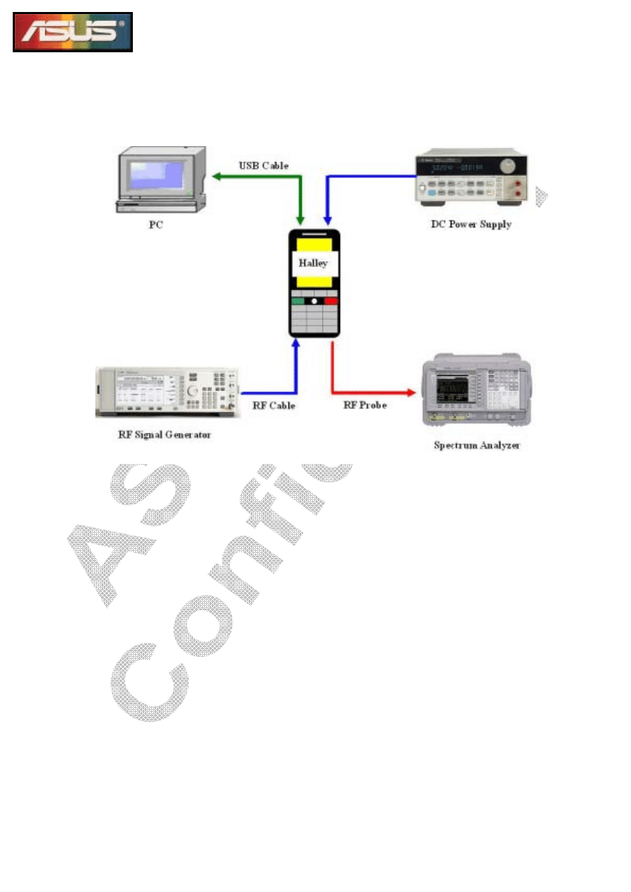
2. Test Environment Setup
(1) Instrument linking
4
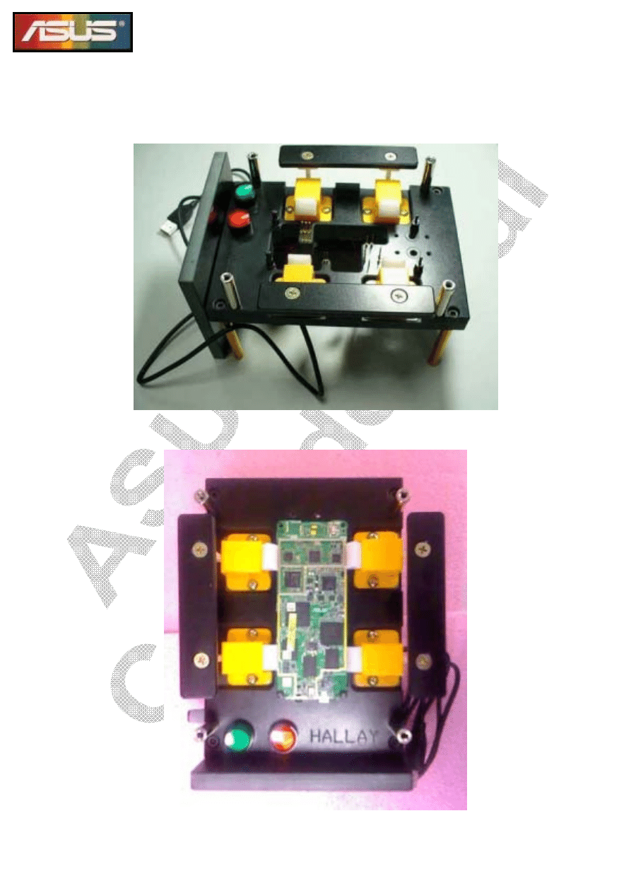
(2) Fixture
Fixture appearance
PCB on fixture (front view)
5
PCB on fixture (rear view)
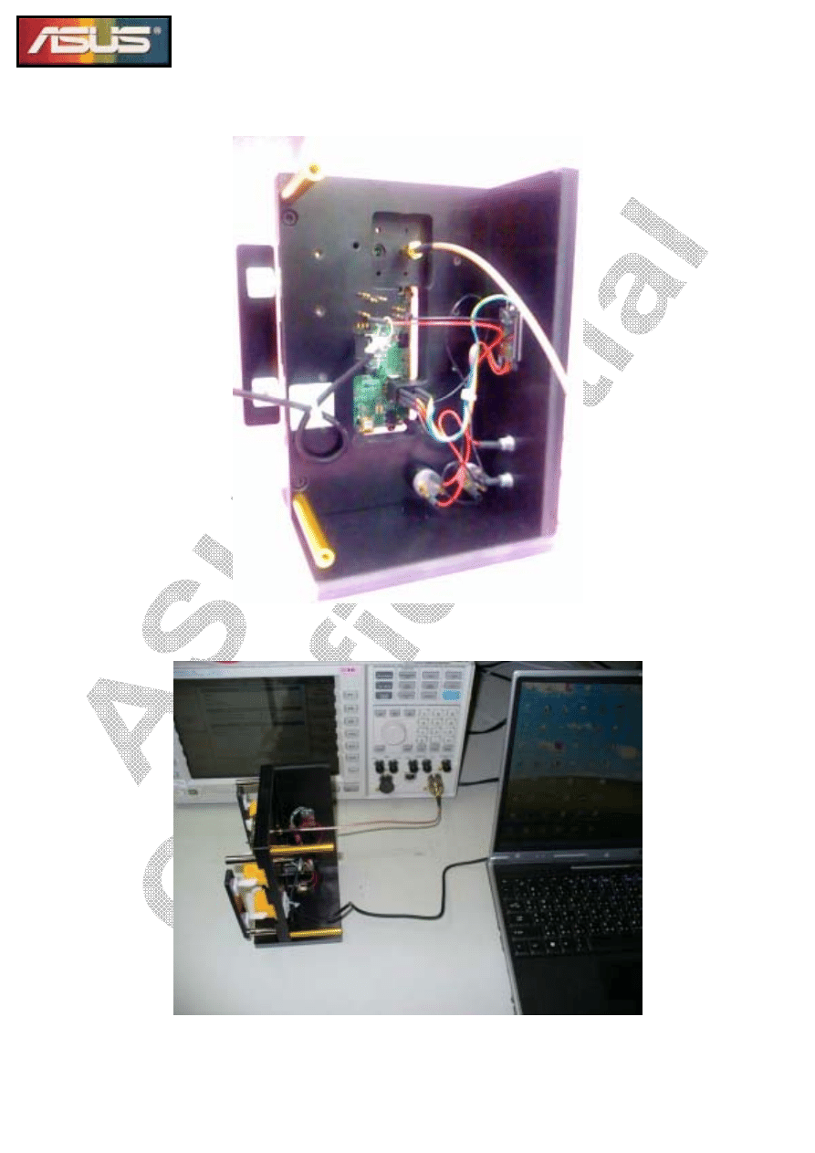
Calibration and RF test setup
6
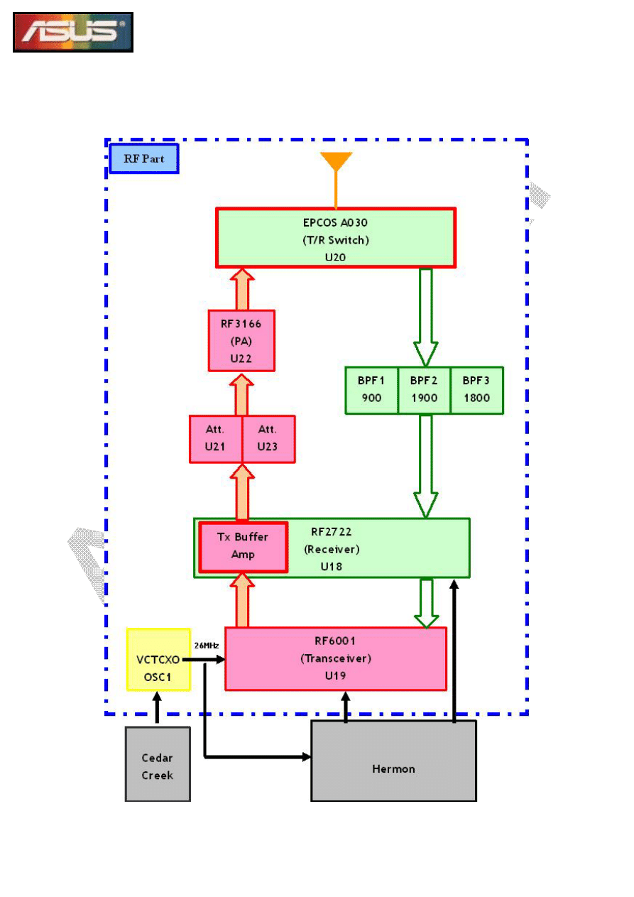
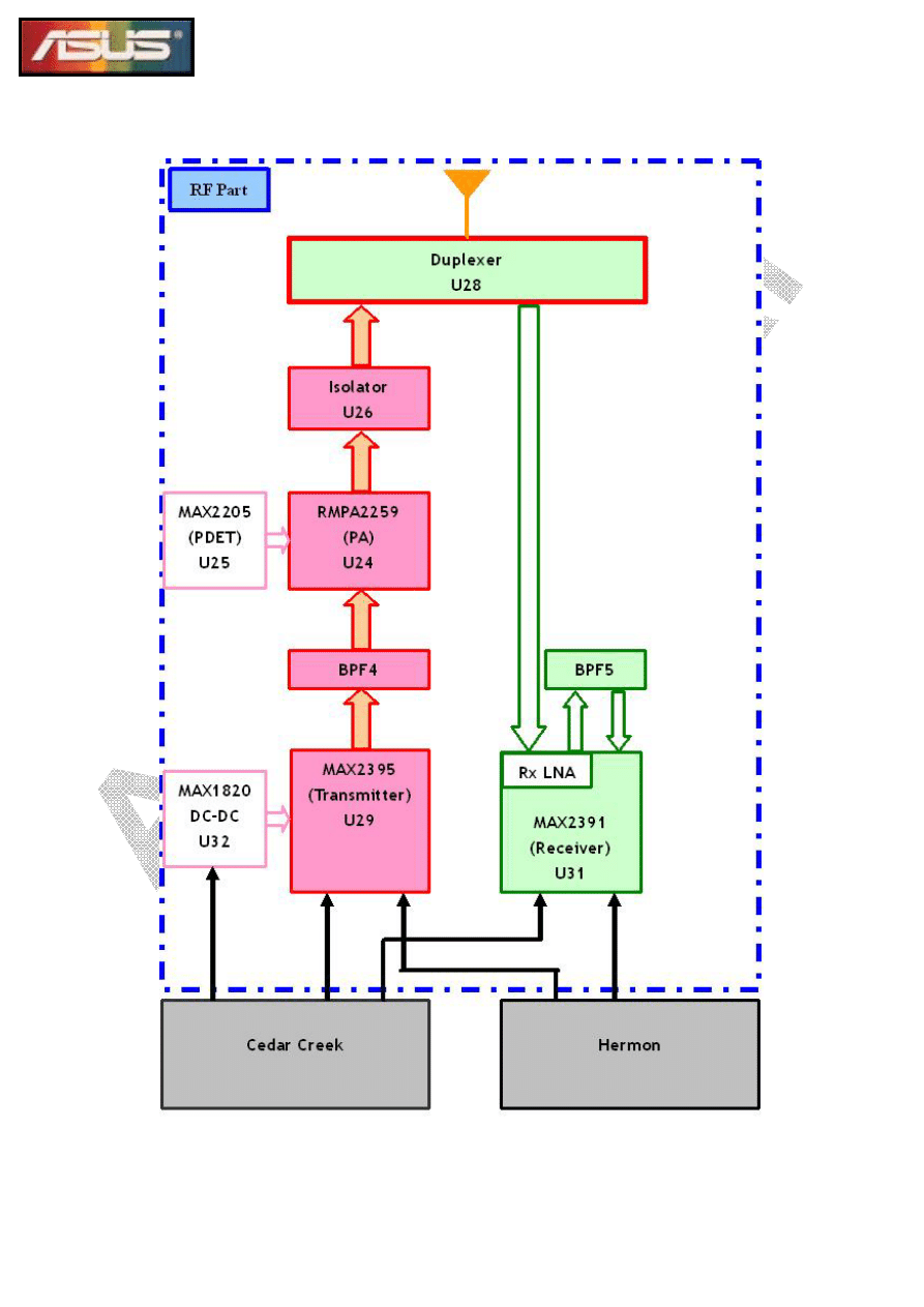
3. RF Block Diagram
(1) GSM block diagram
7
(2) WCDMA block diagram

8
4. RF Tx/Rx Path and Test Points
How RF signal is transmitted and received between components on Halley PCB
is explained in this section. It is important to realize RF transmission path (Tx) and
receiving path (Rx) before starting out to repair NG PCB, because engineers need to
choose proper test points which assist us to distinguish where the problem is. The
following paragraphs describe both Tx and Rx path in GSM and WCDMA bands. The
related test points are listed in the following figures.
(1) GSM Tx/Rx path and test points
GSM Tx path
Transceiver, RF6001 (U19), receives IQ signals coming from baseband, and
output signals of RF6001 Pin22 and Pin23 are transmitted into the buffer of receiver,
RF2722. Then RF2722 Pin12 and Pin13 emit the low band signal (GSM900) and high
band signals (DCS1800 or PCS1900) separately.
In the low band, output signal from RF2722 Pin12 passes through C235,
attenuator (U21) and RF3166 (U22) Pin7, power amplifier, sequentially. Transmission
and receiving switch (U20), also named T/R switch, gets the amplified signal from
RF3166 Pin23 via matching circuits. RF signal coming from T/R switch Pin15 is
transmitted to connector (Con6) and radiated via the GSM antenna of Halley.
In the high band, output signal from RF2722 Pin13 passes through C243,
attenuator (U23) and RF3166 (U22) Pin1, power amplifier, sequentially. Transmission
and receiving switch (U20), also named T/R switch, gets the amplified signal from
RF3166 Pin30 via matching circuits. RF signal coming from T/R switch Pin15 is
transmitted to connector (Con6) and radiated via the GSM antenna of Halley.
GSM Rx path
RF signals, receiving from base stations via the GSM antenna, pass through
connector (Con6) and T/R switch Pin15 (U20) sequentially. There are three output
pins of T/R switch, including Pin2, Pin4, and Pin5. The output path which RF signal
is transmitted depends on band selection of T/R switch.
In GSM900 band, the output signal which is transmitted from T/R switch Pin2
passes through SAW filter (BPF1) and matching circuits sequentially. Upon RF2722
(U18) receiving the signal, it is amplified in the Low Noise Amplifier (LNA) of the
receiver, down converted the signal’s frequency and transformed into IQ signals. The
IQ signals from RF2722 Pin20, Pin21, Pin22, and Pin23 travel to the transceiver
RF6001 (U19). The transceiver RF6001 transfers the signals to the baseband signals.

9
In DCS1800 band, the output signal which is transmitted from T/R switch Pin5
passes through SAW filter (BPF3) and matching circuits sequentially. Upon RF2722
(U18) receiving the signal, it is amplified in the Low Noise Amplifier (LNA) of the
receiver, down converted the signal’s frequency and transformed into IQ signals. The
IQ signals from RF2722 Pin20, Pin21, Pin22, and Pin23 travel to the transceiver
RF6001 (U19). The transceiver RF6001 transfers the signals to the baseband signals.
In PCS1900 band, the output signal which is transmitted from T/R switch Pin4
passes through SAW filter (BPF1) and matching circuits sequentially. Upon RF2722
(U18) receiving the signal, it is amplified in the Low Noise Amplifier (LNA) of the
receiver, down converted the signal’s frequency and transformed into IQ signals. The
IQ signals from RF2722 Pin20, Pin21, Pin22, and Pin23 travel to the transceiver
RF6001 (U19). The transceiver RF6001 transfers the signals to the baseband signals.
10
GSM Tx/Rx test points
Bottom side
Top side

11
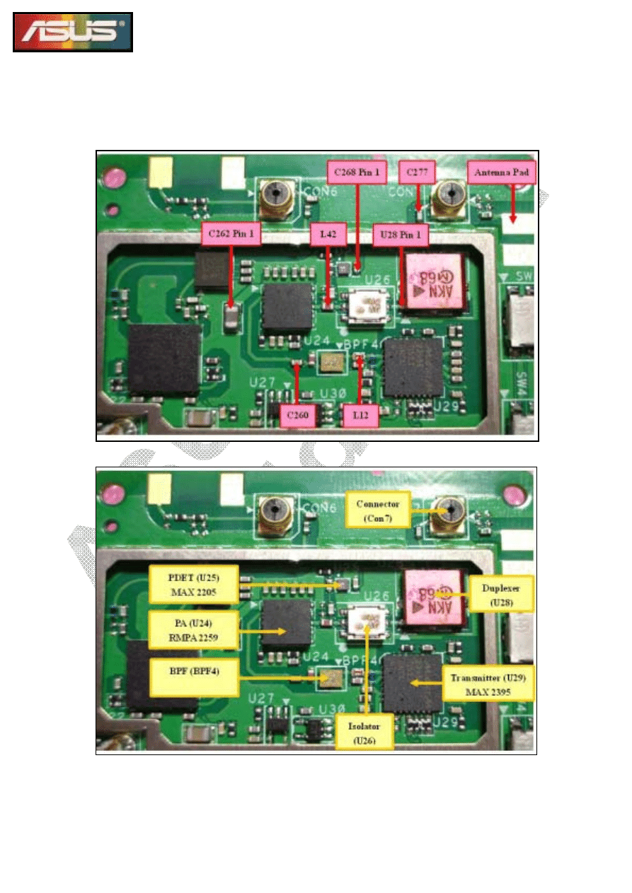
(2) WCDMA Tx/Rx path and test points
WCDMA Tx path
The output signal from transmitter MAX2390 Pin2 travels to SAW filter (BPF4),
and RMPA2259 Pin2 sequentially. The boosted power coming from RMPA2259 Pin8
passes through isolator (U26), duplexer Pin1 (U28), and connector (Con7). At last, the
RF signal is radiated via WCDMA antenna of Halley.
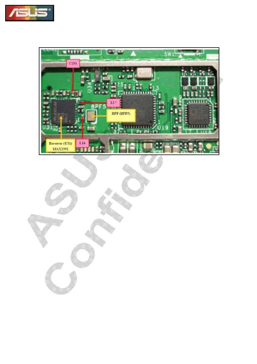
WCDMA Rx path
RF signal in WCDMA, receiving from base stations via the WCDMA antenna,
passes through connector (Con7) and duplexer Pin3 sequentially. MAX2391 Pin1
(U31), built-in LNA, receives the signal from duplexer. Then the signal is transmitted
to SAW filter (BPF5) and returns to receiver MAX2391 again. After down converting
the signal’s frequency and transforming into IQ signals, the IQ signals from
MAX2391 Pin20, Pin21, Pin22, and Pin23 travel to baseband.
12
WCDMA Tx/Rx test points
Bottom side
13
Top side

14
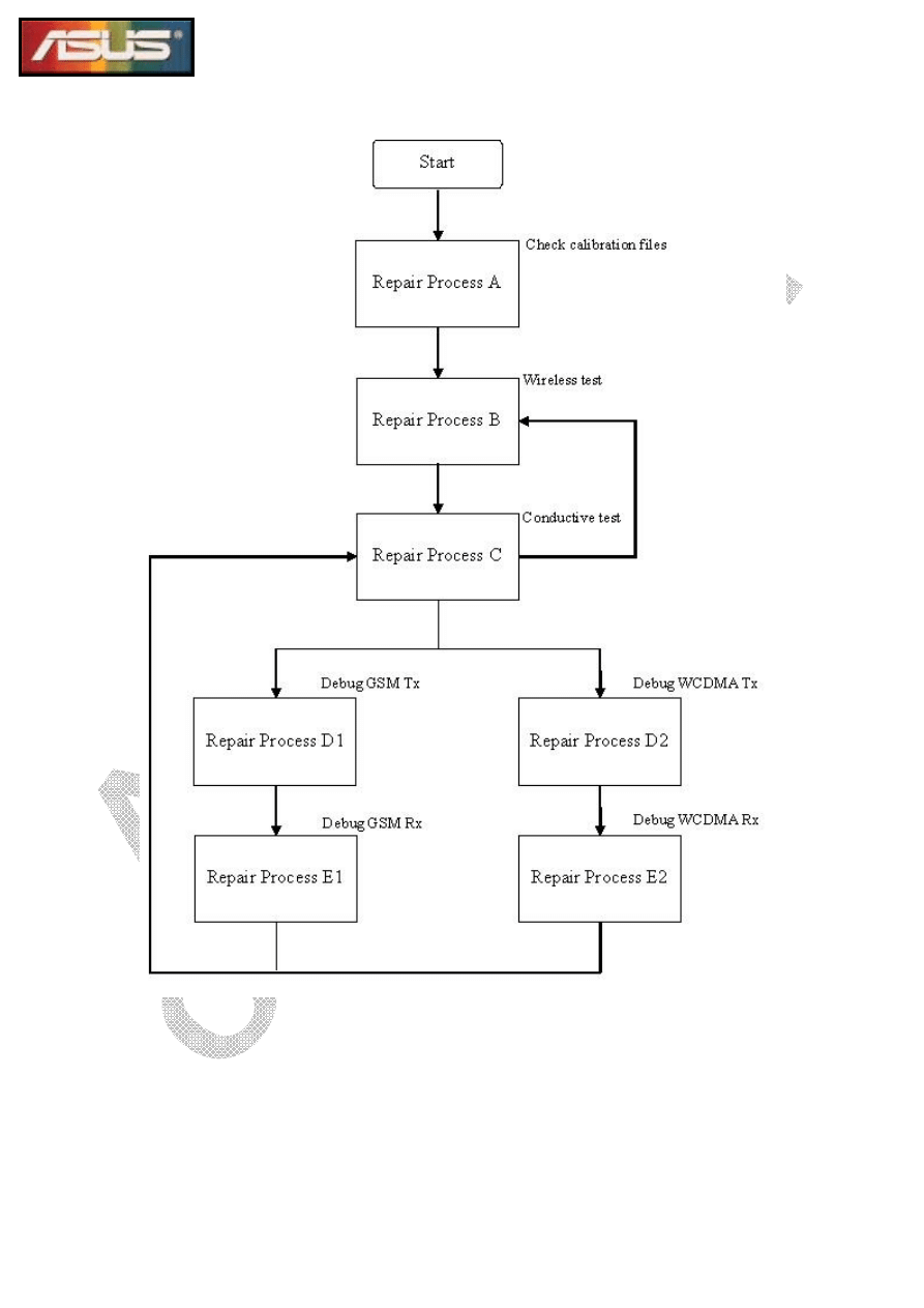
5. Procedures of Repair
The following flow chart shows repair’s procedures that comprise a series of
repair processes. The purpose of each repair processes is to check the cause of
different RF performance defects.
Calibration files should be confirmed first to guarantee existence of RF
parameters in FDI. After wireless and conductive test, engineers can find out where
the problem is. Therefore, engineers properly recognize that the defect comes from
either antenna contact or RF circuits. If the defect results from RF circuit, the next
procedure is to disassemble and debug Tx/Rx path.
It is very important that conductive and wireless test should be done again to
make sure that Halley operates properly after any debug process. Each repair process
is described specifically in following sections.
15
16
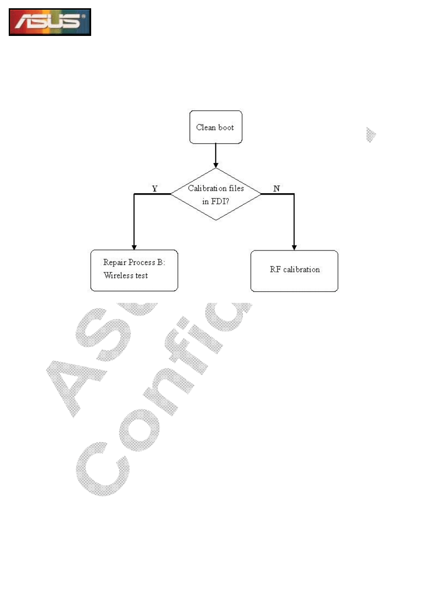
(1) Repair Process A: check calibration files
The flow chart of Repair Process A is shown below.
The purpose of this repair process is to check calibration files in FDI. Without
calibration files, Halley can’t keep good RF performance. Moreover, making a phone
call might operate improperly.
17
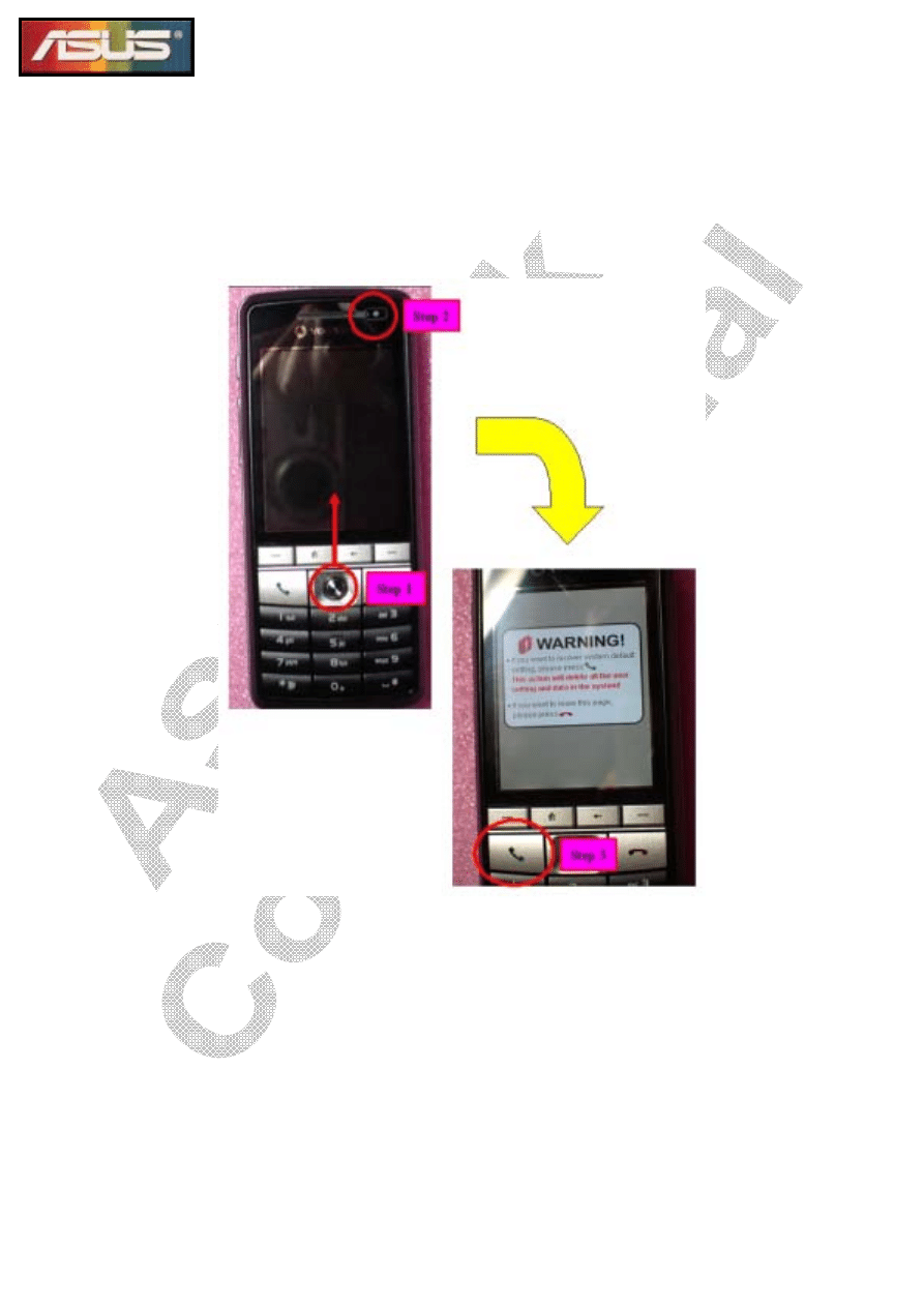
The detail steps of Repair Process A are listed as follows.
a. Clean boot: push “Direction key” upward first, and then press “Power key”.
When “WARNING” is shown on panel, press “Send key”. The figure below shows
clean boot method.
b. Check calibration files in FDI by using IFL tool. There shall be three
calibration files in FDI. The names of the calibration files are as follows,
PcCalData.nvm
aplp_rf_analysis.nvm
aplp_rf_calibration.nvm.
c. If all calibration files exist in FDI, go to next Repair Process B: Wireless test.
Otherwise, the PCB which calibration files are lost needs to be calibrated.

18
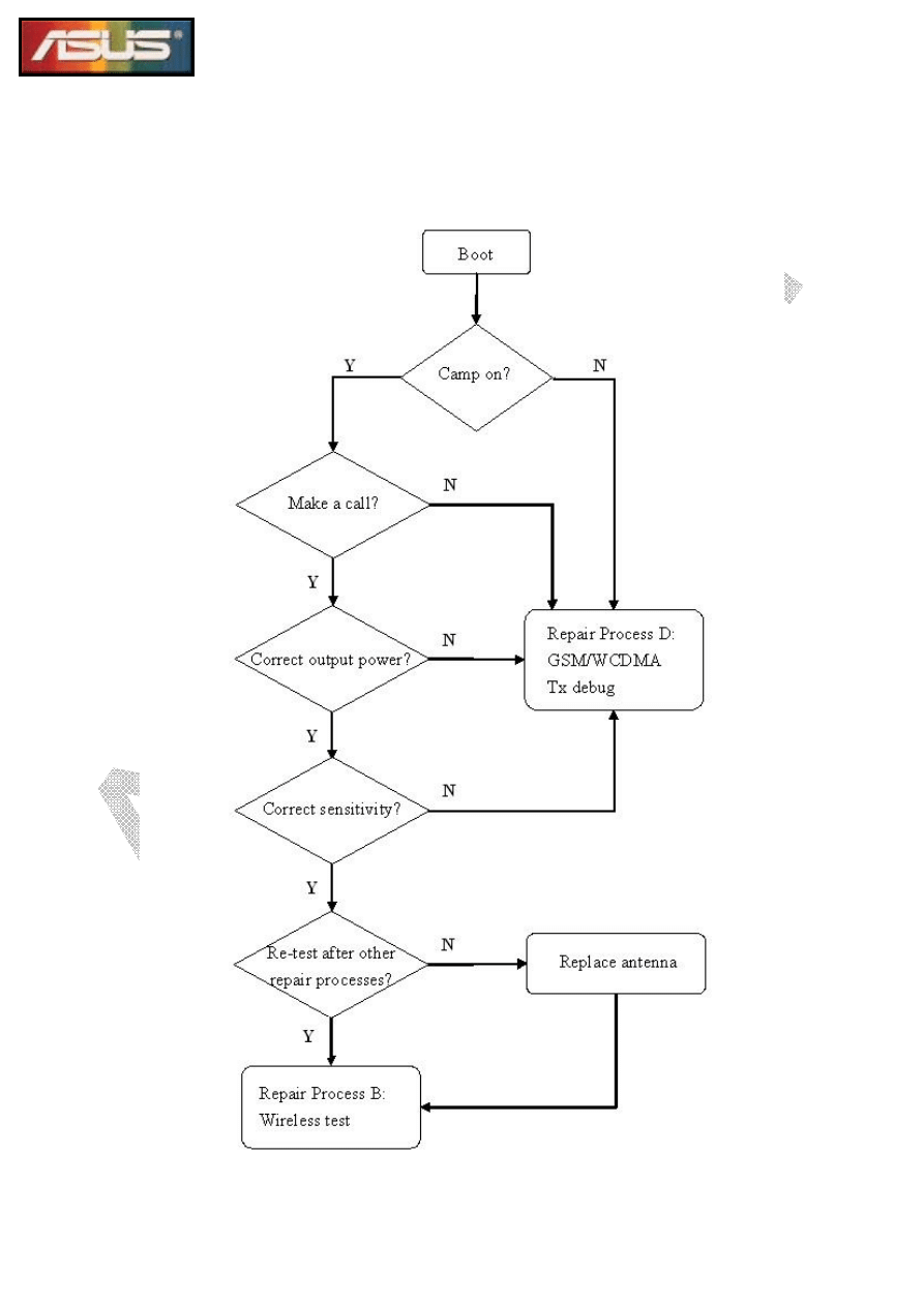
(2) Repair Process B: GSM/WCDMA wireless test
The flow chart of Repair Process B is shown below.

19
The purpose of this repair process is to distinguish problems between antenna
and RF circuit that cause weak RF performance. Besides, wireless test is a previous
analysis of all RF tests. Moreover, engineers utilize wireless test to confirm that
antenna performance is not affected after re-assembling.
The detail steps of Repair Process B are listed as follows.
a. Put a golden sample of Halley into a shielding box and link to a tester (Agilent
8960 or R&S CMU200). Then, record its location and path loss.
b. At the same position that the golden sample was located, put problematic
Halley into the shielding box. After that, wait for Halley registering at the tester.
c. After attaching to the network, make a phone call.
d. Measure maximum output power and sensitivity. The test requirements of
maximum output power and sensitivity shall not exceed the range listed in the
following table.
e. If any of previous steps (b. ~ d.) is failed, consequently enter next process,
Repair Process C: GSM/WCDMA conductive test.
f. If all previous steps (b. ~ d.) are passed, it means that nothing happens.
Therefore, need to clarify customer’s complaints and try to understand user’s
behaviors.
Channel
Power
Level
Power
Requirements
Sensitivity
Requirements
GSM 900
62 5
29.3~35.3
dBm
Refer to
golden sample
DCS 1800
700 0
26.0~32.0
dBm
Refer to
golden sample
PCS 1900
661 0
26.0~32.0
dBm
Refer to
golden sample
WCDMA
10700
All up
(24 dBm)
20.8~25.5 dBm
Refer to
golden sample
20
(3) Repair Process C: GSM/WCDMA conductive test
The flow chart of Repair Process C is shown below.

21
The purpose of this repair process is to reduce the scope of RF problems. Due to
smaller measuring tolerance of conductive test, it is helpful to focus on either GSM
band or WCDMA band. Moreover, engineers can obtain further information about Tx
and Rx path of RF circuits.
The detail steps of Repair Process C are listed as follows.
a. Connect Halley which needs to repair with a tester by a RF cable. After that,
wait for registering at the tester. (Agilent 8960 or R&S CMU200)
b. After attaching to the network, make a phone call.
c. Measure maximum output power and sensitivity. The test requirements of
maximum output power and sensitivity shall not exceed the range listed in the
following table.
d. If any of previous steps (a. ~ c.) is failed, consequently execute “MMI test
program” (also named “2577”) and disassemble Halley later for RF hardware circuit
debug (Repair Process D1: GSM Tx debug or Repair Process D2: WCDMA Tx
debug).
e. If all steps (a. ~ c.) are passed but the previous process, wireless test, is failed,
it means antenna shall be replaced. In another case, Halley needs verification of
conductive test and shall pass previous steps (a. ~ c.) after other successful debug
processes. At this time, the next step is to do wireless test.
Channel
Power
Level
Power
Requirements
Sensitivity
Requirements
GSM 900
62 5
31.3~33.3
dBm
-106.0 dBm
DCS 1800
700 0
28.0~30.0
dBm
-105.0 dBm
PCS 1900
661 0
28.0~30.0
dBm
-105.0 dBm
WCDMA
10700
All up
(24 dBm)
21.5~25.0 dBm
-108.2 dBm
22
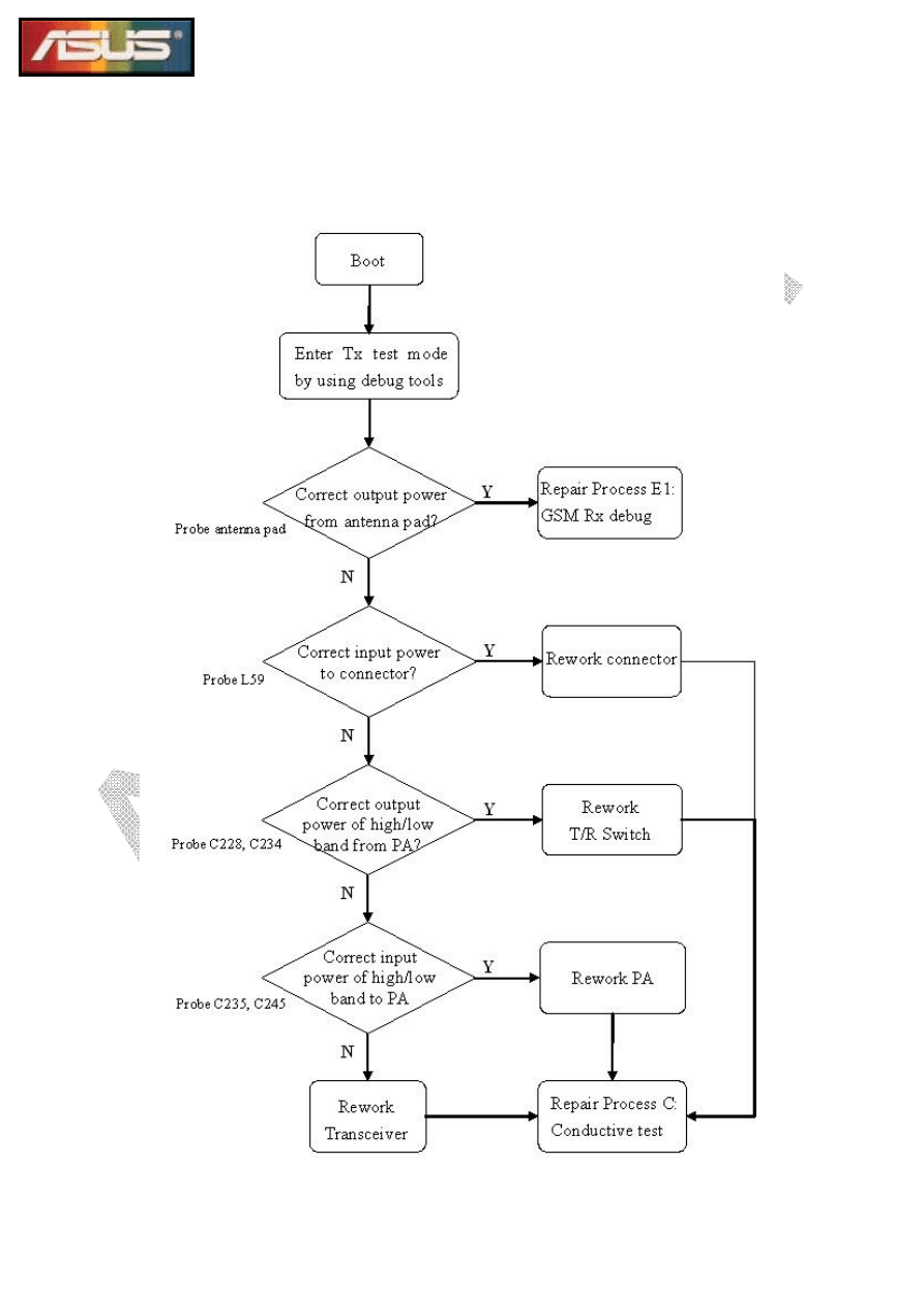
(4) Repair Process D1: GSM Tx debug
The flow chart of Repair Process D1 is shown below.

23
The purpose of this repair process is to find out where the problem is on GSM Tx
path. In other words, engineers can judge the defect component on RF path by using
“Debug tool”. Debug tool makes Halley into test mode so that PA can transmit power
continuously.
The usage of debug tool can be referred to “Debug tool user guide” provided by
Halley ATS engineers. Related parameters of debug tool are prescribed in the
following table.
Channel
PCL
Tx
Frequency
PAG_Value
DAC1V
GSM 900
62 5 902.4
MHz 555 5200
DCS 1800
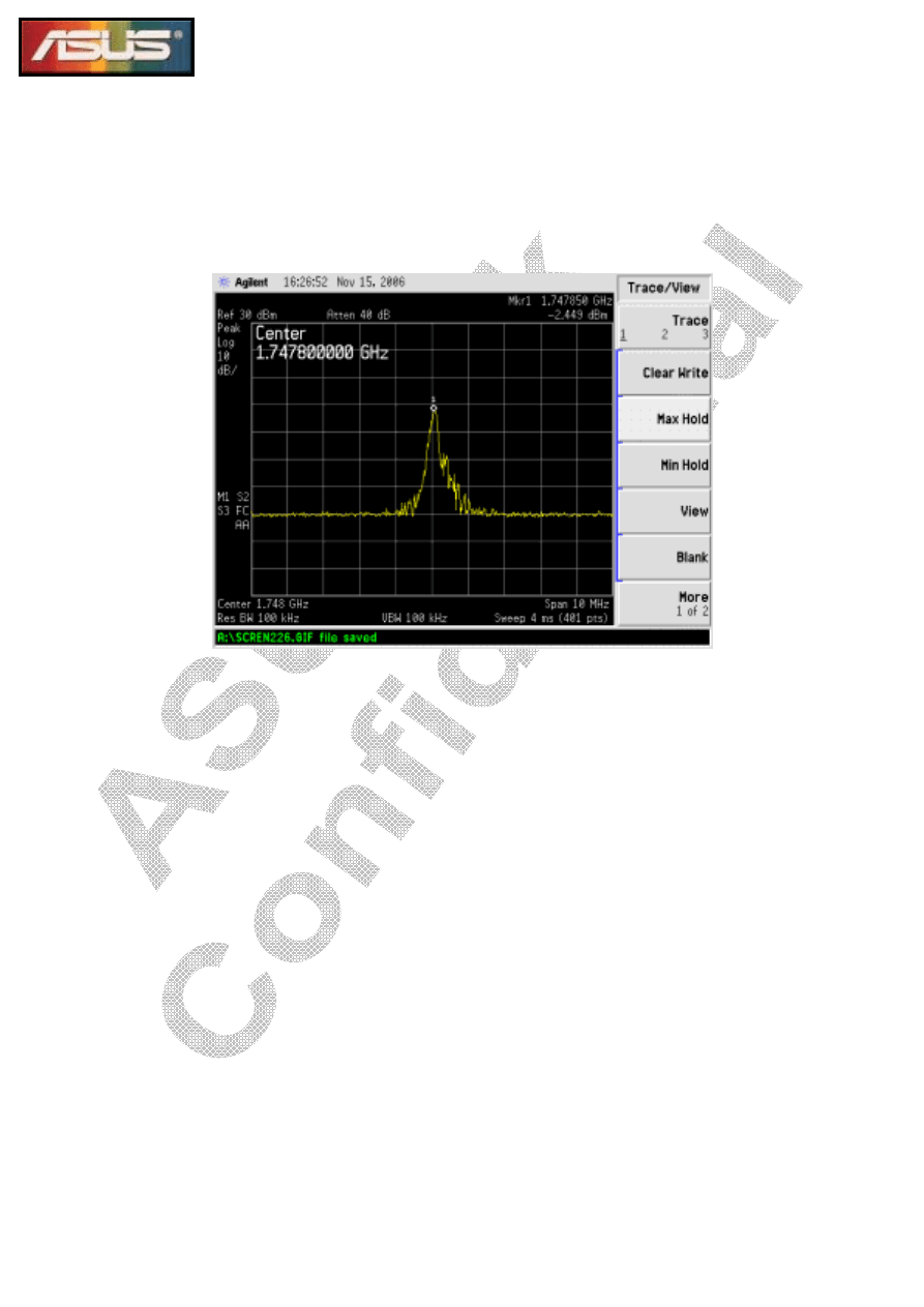
700 0 1747.8
MHz 560 5200
PCS 1900
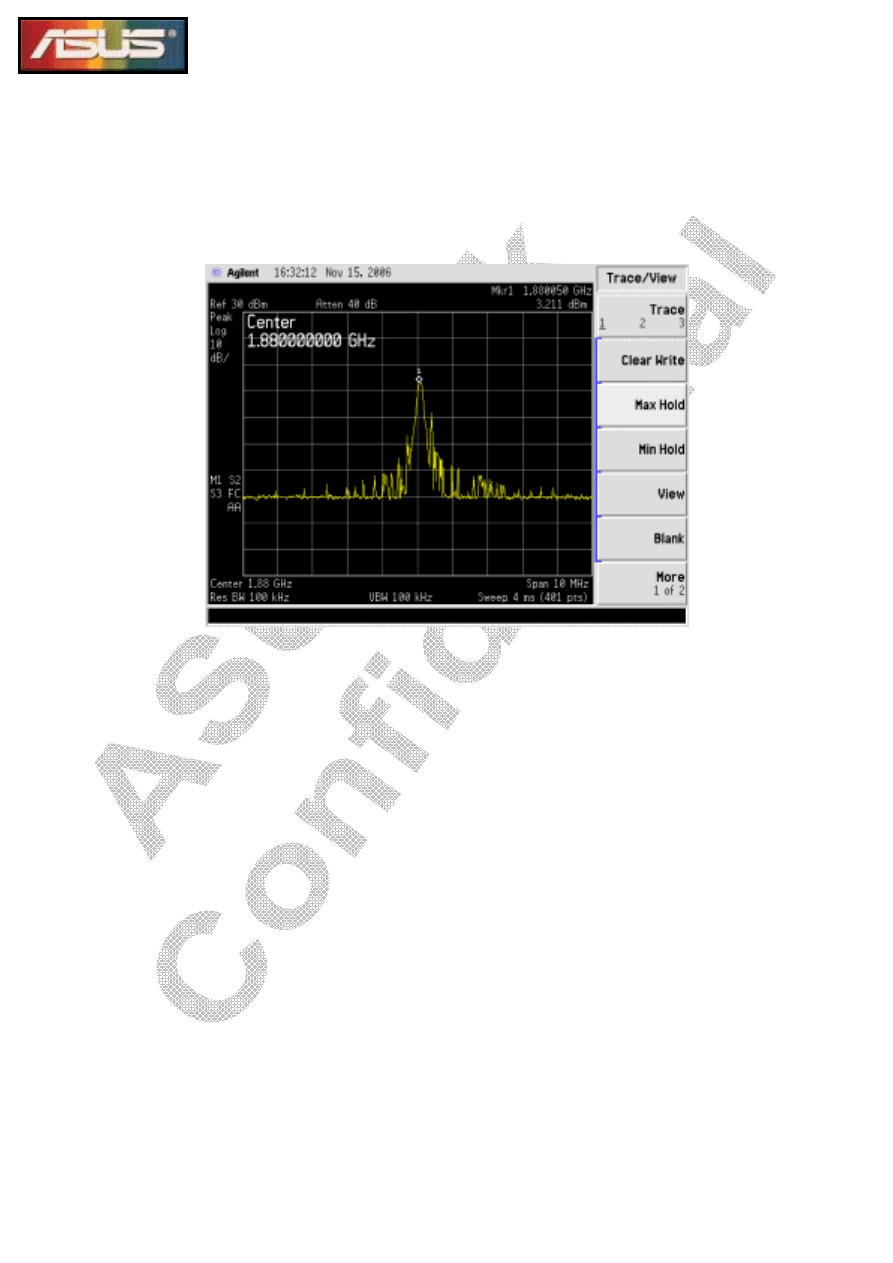
661 0 1880.0
MHz 525 5200
The detail steps of Repair Process D1 are listed as follows.
GSM 900 Tx debug
a. Spectrum analyzer connects with a high impedance probe. Execute GSM
debug tool and set parameters in the above table.
b. Use the high impedance probe to sequentially measure RF power of test points
on GSM Tx path, including antenna pad, L59, C228, and C235. Corresponding
locations are shown in “4. RF Tx/Rx Path and Test Points.” Furthermore,
measurement error of RF power on each test point is unavoidable due to measurement
skills and methods of using high impedance probe.
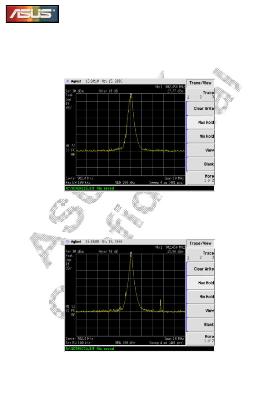
c. Antenna pad: all components on Tx path are good if power is measured from
antenna pad within 25dBm~32dBm. In this case, engineers shall go to next repair
process, Repair Process E1: GSM Rx debug.
24
d. L59: Check whether GSM RF connector (CON6) is good or not. CON6 needs
to be reworked if power is measured within 25dBm~ 32dBm on L59, and no signal is
measured from antenna pad. The following figure is an example of L59 signal
measurement on the spectrum analyzer.
e. C228: Check whether T/R switch (U20) is good or not. T/R switch needs to be
reworked if power is measured within 25dBm~ 32dBm on C228, and no signal is
measured on L59. The following figure is an example of C228 signal measurement on
the spectrum analyzer.
25
f. C235: Check whether PA (U22) is good or not. PA needs to be reworked if
power is measured within -6dBm~ 0dBm on C236, and no signal is measured on
C228. Besides, if no output power is measured on C235, transceiver (U19) needs to
be reworked. The following figure is an example of C235 signal measurement on the
spectrum analyzer.
DCS 1800 Tx debug
a. Spectrum analyzer connects with a high impedance probe. Execute GSM
debug tool and set parameters in the above table.
b. Use the high impedance probe to sequentially measure RF power of test points
on GSM Tx path, including antenna pad, L59, C234, and C245. Corresponding
locations are shown in “4. RF Tx/Rx Path and Test Points.” Furthermore,
measurement error of RF power on each test point is unavoidable due to measurement
skills and methods of using high impedance probe.
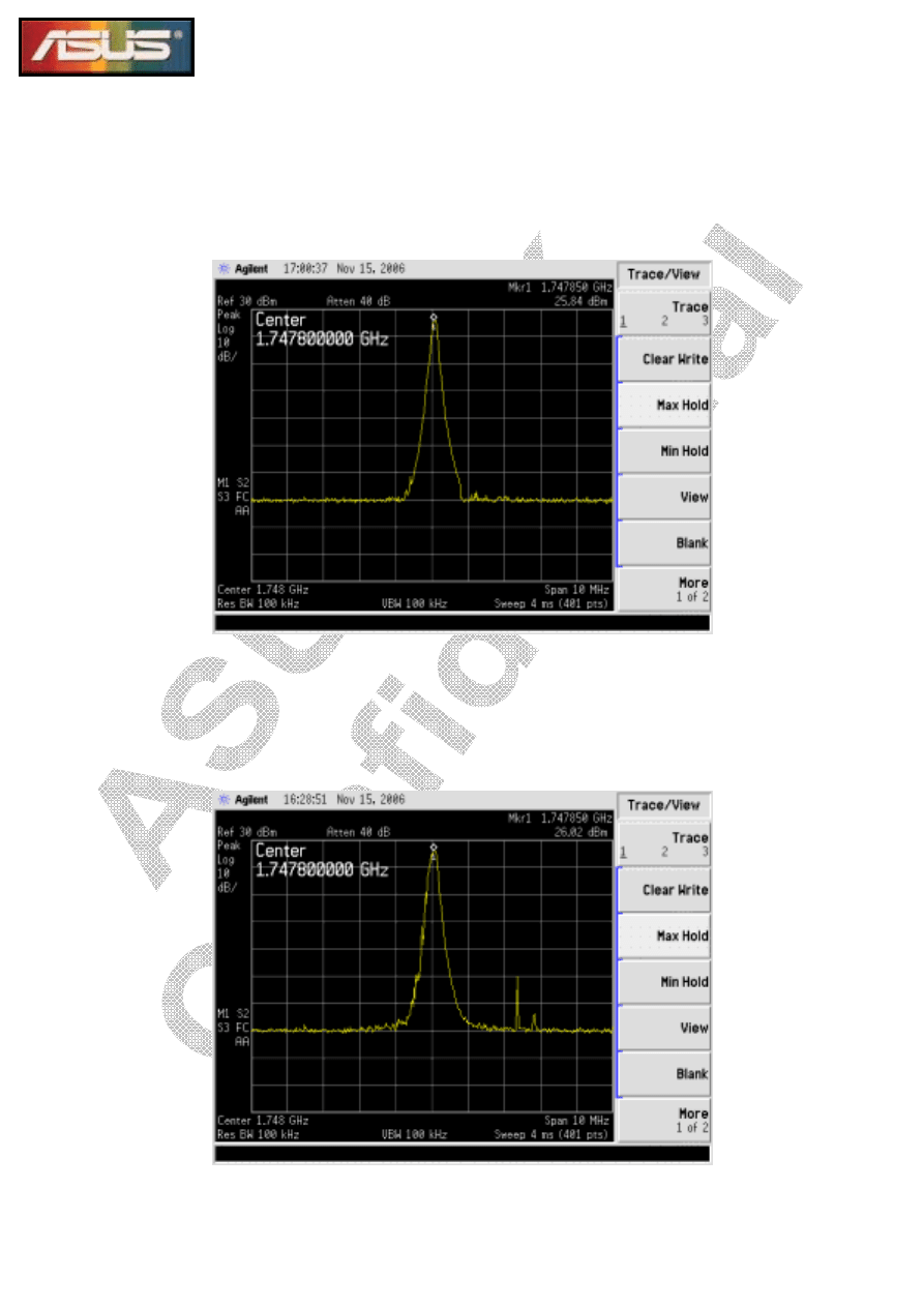
c. Antenna pad: all components on Tx path are good if power is measured from
antenna pad within 25dBm~32dBm. In this case, engineers shall go to next repair
process, Repair Process E1: GSM Rx debug.
26
d. L59: Check whether GSM RF connector (CON6) is good or not. CON6 needs
to be reworked if power is measured within 25dBm~ 32dBm on L59, and no signal is
measured from antenna pad. The following figure is an example of L59 signal
measurement on the spectrum analyzer.
e. C234: Check whether T/R switch (U20) is good or not. T/R switch needs to be
reworked if power is measured within 25dBm~ 32dBm on C228, and no signal is
measured on L59. The following figure is an example of C234 signal measurement on
the spectrum analyzer.
27
f. C245: Check whether PA (U22) is good or not. PA needs to be reworked if
power is measured within -6dBm~ 0dBm on C245, and no signal is measured on
C234. Besides, if no output power is measured on C245, transceiver (U19) needs to
be reworked. The following figure is an example of C245 signal measurement on the
spectrum analyzer.
PCS 1900 Tx debug
a. Spectrum analyzer connects with a high impedance probe. Execute GSM
debug tool and set parameters in the above table.
b. Use the high impedance probe to sequentially measure RF power of test points
on GSM Tx path, including antenna pad, L59, C228, and C235. Corresponding
locations are shown in “4. RF Tx/Rx Path and Test Points.” Furthermore,
measurement error of RF power on each test point is unavoidable due to measurement
skills and methods of using high impedance probe.
c. Antenna pad: all components on Tx path are good if power is measured from
antenna pad within 25dBm~32dBm. In this case, engineers shall go to next repair
process, Repair Process E1: GSM Rx debug.

28
d. L59: Check whether GSM RF connector (CON6) is good or not. CON6 needs
to be reworked if power is measured within 25dBm~ 32dBm on L59, and no signal is
measured from antenna pad. The following figure is an example of L59 signal
measurement on the spectrum analyzer.
e. C234: Check whether T/R switch (U20) is good or not. T/R switch needs to be
reworked if power is measured within 25dBm~ 32dBm on C228, and no signal is
measured on L59. The following figure is an example of C234 signal measurement on
the spectrum analyzer.
29
f. C245: Check whether PA (U22) is good or not. PA needs to be reworked if
power is measured within -6dBm~ 0dBm on C245, and no signal is measured on
C234. Besides, if no output power is measured on C245, transceiver (U19) needs to
be reworked. The following figure is an example of C245 signal measurement on the
spectrum analyzer.
30
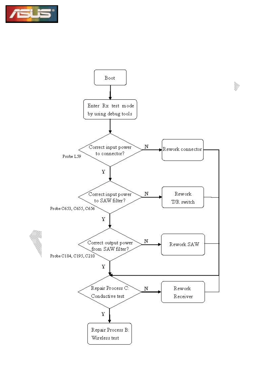
(5) Repair Process E1: GSM Rx debug
The flow chart of Repair Process E1 is shown below.

31
The purpose of this repair process is to find out where the problem is on GSM
Rx path. In other words, engineers can judge the defect component on RF path by
using “Debug tool” and RF signal generator. Debug tool makes Halley into test mode
and keeps Rx path receiving CW (continuous wave) from the generator.
The usage of debug tool can be referred to “Debug tool user guide” provided by
Halley ATS engineers. Related parameters of debug tool and recommended output
power from the generator are prescribed in the following table.
Channel
Rx
Frequency
Generator
power
GSM 900
62
947.4 MHz
-20 dBm
DCS 1800
700
1842.8 MHz
-20 dBm
PCS 1900
661
1960.0 MHz
-20 dBm
The detail steps of Repair Process E1 are listed as follows.
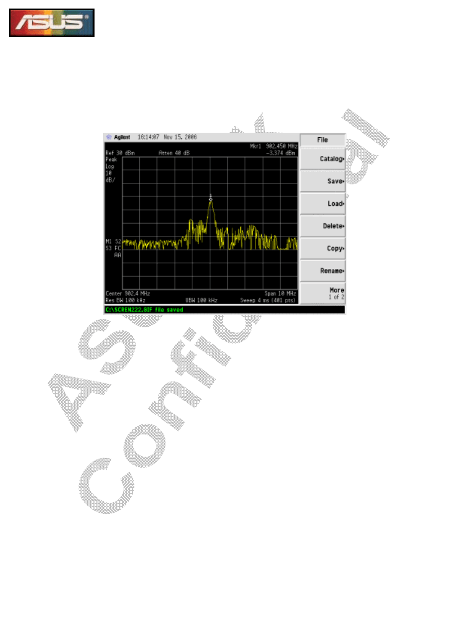
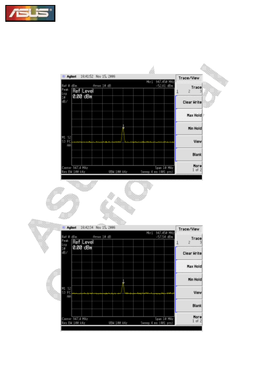
GSM 900 Rx debug
a. Set RF signal generator to emit CW with corresponding frequency and
transmit power into Halley GSM connector via RF cable and a RF adapter (MS-162).
Spectrum analyzer connects with a high impedance probe. Execute GSM debug tool
and set parameters in the above table.
b. Use the high impedance probe to sequentially measure RF power of test points
on GSM Rx path, including L59, C653, and C184. Corresponding locations are
shown in “4. RF Tx/Rx Path and Test Points.” Furthermore, measurement error of RF
power on each test point is unavoidable due to measurement skills and methods of
using high impedance probe.
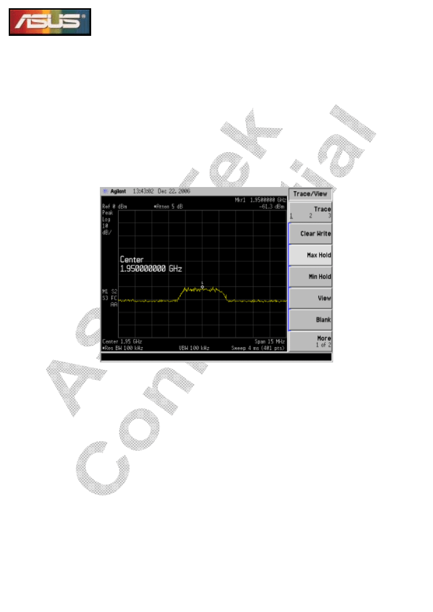
c. L59: Check whether GSM RF connector (CON6) is good or not. CON6 needs
to be reworked if no RF signal is measured on L59.
32
d. C653: Check whether T/R switch (U20) is good or not. T/R switch needs to be
reworked if RF signal emitted by the signal generator is measured on L59, and no
power is detected on C653. The following figure is an example of C653 signal
measurement on the spectrum analyzer.
e. C184: Check whether SAW filter (BPF1) is good or not. BPF1 needs to be
reworked if RF signal emitted by the signal generator is measured on C653, and no
power is detected on C184. The following figure is an example of C184 signal
measurement on the spectrum analyzer.
33
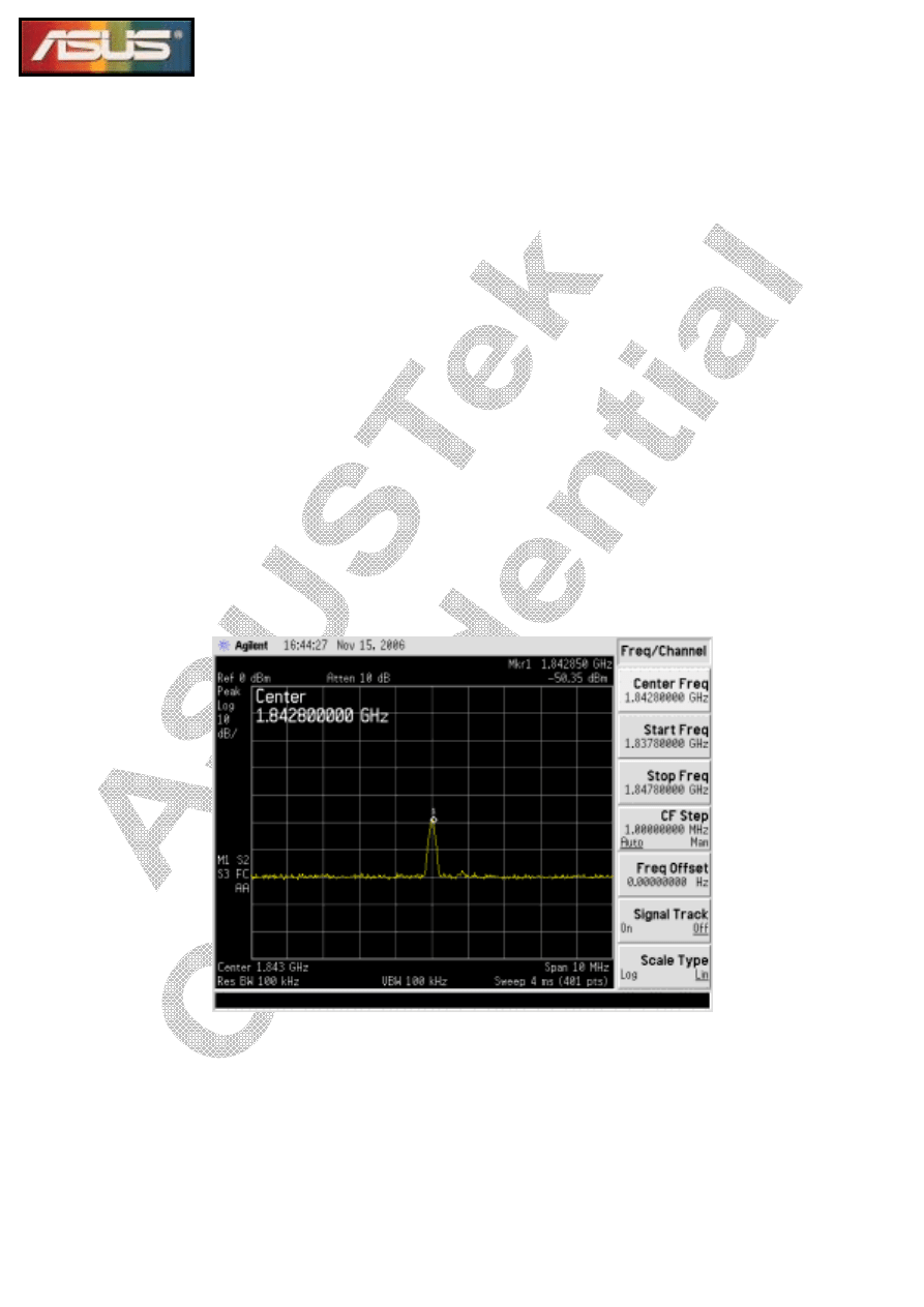
DCS 1800 Rx debug
a. Set RF signal generator to emit CW with corresponding frequency and
transmit power into Halley GSM connector via a RF cable and a RF adapter (MS-162).
Spectrum analyzer connects with a high impedance probe. Execute GSM debug tool
and set parameters in the above table.
b. Use the high impedance probe to sequentially measure RF power of test points
on GSM Rx path, including L59, C656, and C210. Corresponding locations are
shown in “4. RF Tx/Rx Path and Test Points.” Furthermore, measurement error of RF
power on each test point is unavoidable due to measurement skills and methods of
using high impedance probe.
c. L59: Check whether GSM RF connector (CON6) is good or not. CON6 needs
to be reworked if no RF signal is measured on L59.
d. C656: Check whether T/R switch (U20) is good or not. T/R switch needs to be
reworked if RF signal emitted by the signal generator is measured on L59, and no
power is detected on C656. The following figure is an example of C656 signal
measurement on the spectrum analyzer.
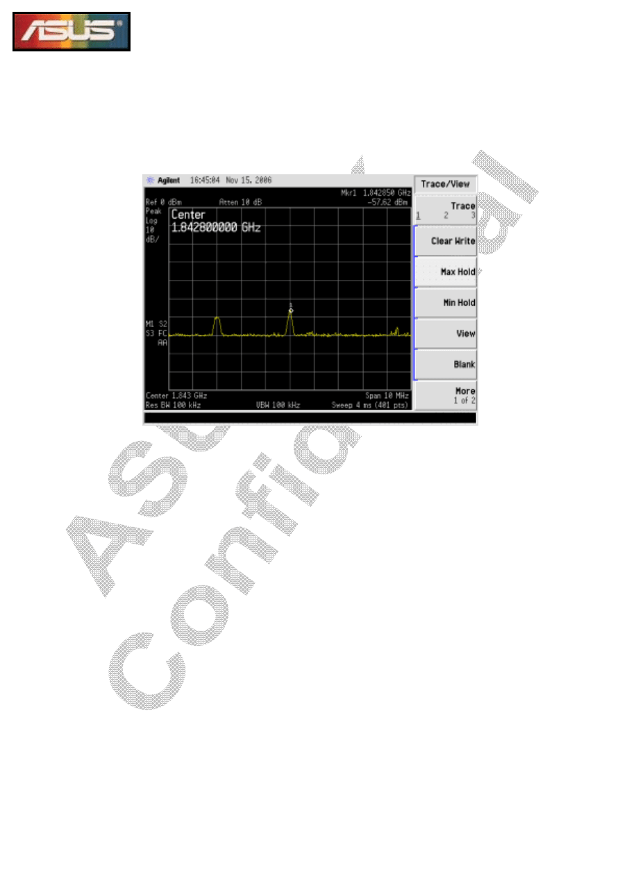
34
e. C210: Check whether SAW filter (BPF3) is good or not. BPF3 needs to be
reworked if RF signal emitted by the signal generator is measured on C656, and no
power is detected on C210. The following figure is an example of C210 signal
measurement on the spectrum analyzer.
35
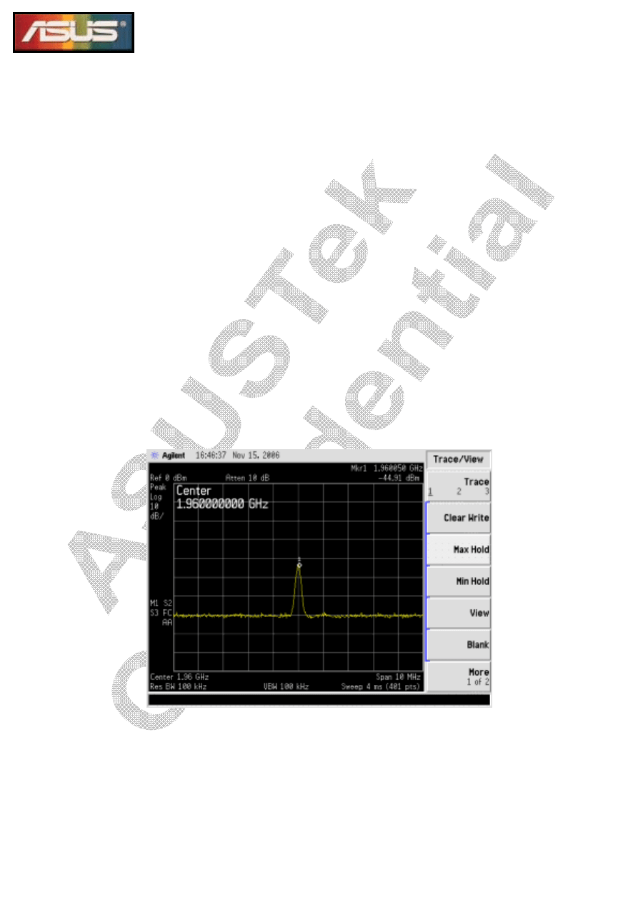
PCS 1900 Rx debug
a. Set RF signal generator to emit CW with corresponding frequency and
transmit power into Halley GSM connector via a RF cable and a RF adapter (MS-162).
Spectrum analyzer connects with a high impedance probe. Execute GSM debug tool
and set parameters in the above table.
b. Use the high impedance probe to sequentially measure RF power of test points
on GSM Rx path, including L59, C655, and C195. Corresponding locations are
shown in “4. RF Tx/Rx Path and Test Points.” Furthermore, measurement error of RF
power on each test point is unavoidable due to measurement skills and methods of
using high impedance probe.
c. L59: Check whether GSM RF connector (CON6) is good or not. CON6 needs
to be reworked if no RF signal is measured on L59.
d. C655: Check whether T/R switch (U20) is good or not. T/R switch needs to be
reworked if RF signal emitted by the signal generator is measured on L59, and no
power is detected on C655. The following figure is an example of C655 signal
measurement on the spectrum analyzer.

36
e. C195: Check whether SAW filter (BPF2) is good or not. BPF2 needs to be
reworked if RF signal emitted by the signal generator is measured on C655, and no
power is detected on C195. The following figure is an example of C195 signal
measurement on the spectrum analyzer.
f. The next process returns to “Repair Process C: GSM/WCDMA conductive
test” after all Rx paths are well in GSM900 band, DCS1800 band, and PCS1900 band.
In a special case, receiver (U18) needs to be reworked if no problem is found on all
Rx paths and conductive test is still failed. Furthermore, the process returns to
wireless test under the condition of passing conductive test.
37
(6) Repair Process D2: WCDMA Tx debug
The flow chart of Repair Process D2 is shown below.
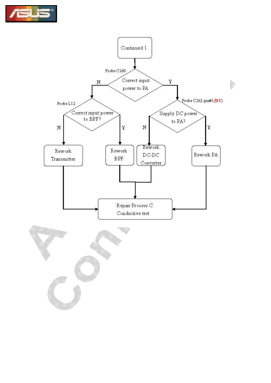
38
39

40
The purpose of this repair process is to find out where the problem is on
WCDMA Tx path. In other words, engineers can judge the defect component on RF
path by using “Debug tool”. Debug tool makes Halley into test mode so that PA can
transmit power continuously.
The usage of debug tool can be referred to “Debug tool user guide” provided by
Halley ATS engineers. Related parameters of debug tool are prescribed in the
following table.
UL Channel
Tx Frequency
Vgc DAC
WCDMA
9750 1950.0
MHz 1024
The detail steps of Repair Process D2 are listed as follows.
a. Spectrum analyzer connects with a high impedance probe. Execute GSM
debug tool and set parameters in the above table.
b. Use the high impedance probe to sequentially measure RF power of test points
on GSM Tx path, including antenna pad, C277, duplexer (U28) Pin1, L42, C268 Pin1,
C260, C262 Pin1, and L12. Furthermore, the signals of C268 Pin1 and C262 Pin1 are
both DC signals instead. Corresponding locations are shown in “4. RF Tx/Rx Path
and Test Points.” Moreover, measurement error of RF power on each test point is
unavoidable due to measurement skills and methods of using high impedance probe.
41
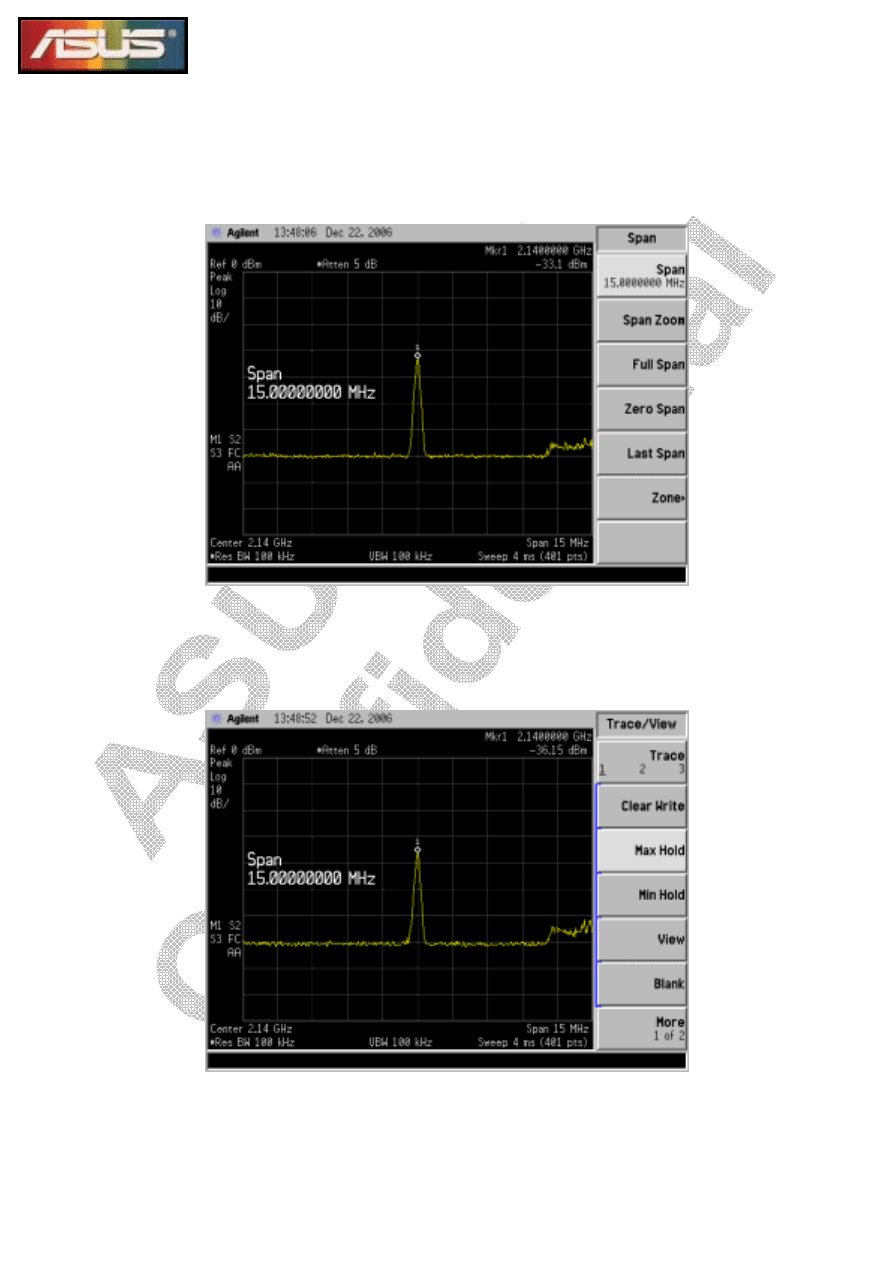
c. Antenna pad: all components on WCDMA Tx path are good if power is
measured from antenna pad within -46dBm~-37dBm. In this case, engineers shall go
to next repair process, Repair Process E2: WCDMA Rx debug.
d. C277: Check whether WCDMA RF connector (CON7) is good or not. CON7
needs to be reworked if power is measured within -46dBm~-37dBm on C277, and no
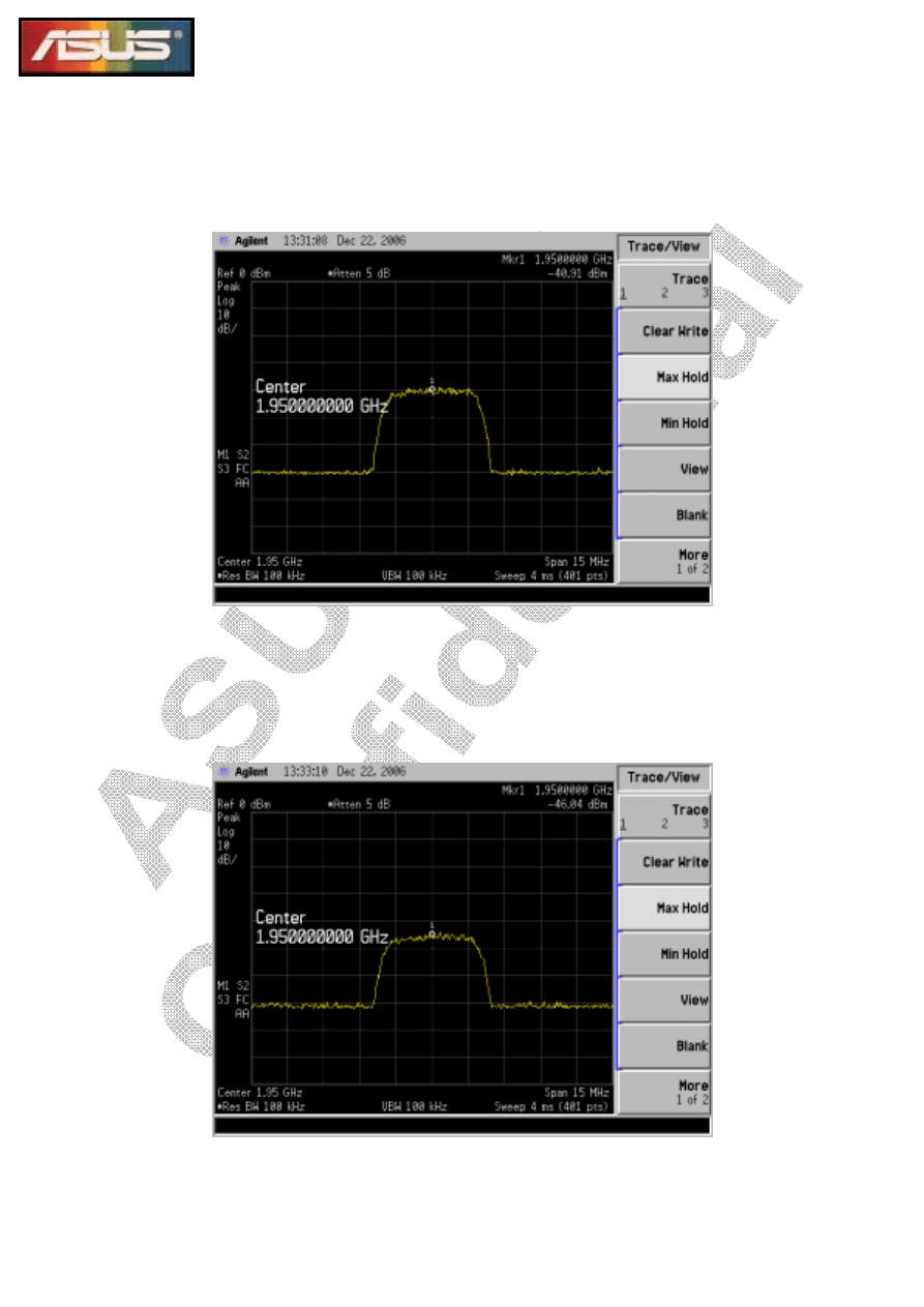
signal is measured from antenna pad. The following figure is an example of C277
signal measurement on the spectrum analyzer.
42
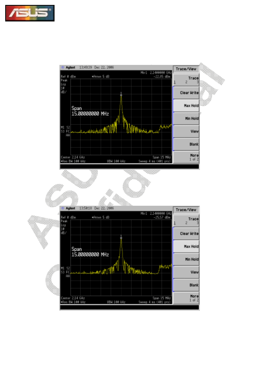
e. U28 Pin1: Check whether duplexer (U28) is good or not. Duplexer needs to be
reworked if power is measured within -46dBm~ -37dBm on U28 Pin1, and no signal
is measured on C277. The following figure is an example of U28 Pin1 signal
measurement on the spectrum analyzer.
f. L42: Check whether isolator (U26) is good or not. CON7 needs to be reworked
if power is measured within -46dBm~-37dBm on C277, and no signal is measured on
U28 Pin1. The following figure is an example of L42 signal measurement on the
spectrum analyzer.
43
g. C268 Pin1(
DC
): Check whether power detector (U28) is good or not. The
main function of power detector is to sense RF signal by means of converting RF to
DC voltage. The voltage level on C268 Pin1 shall be 1.3V ~ 1.5V as maximum output
power, approximate 23.5 dBm, is emitted. Power detector needs to be reworked if no
voltage level is measured in the situation of maximum output power.
h. C260: Check whether PA (U24) operates normally or not. PA needs to be
reworked if DC-DC converter supplies DC voltage to PA and power is measured
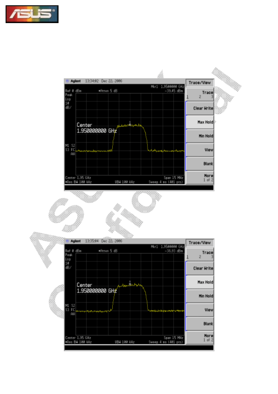
within -63dBm~-55dBm on C260. The following figure is an example of C260 signal
measurement on the spectrum analyzer.
i. C262 Pin1(
DC
): Check whether DC-DC converter (U32) is good or not. The
voltage level on C262 Pin1 shall be 2.7V ~ 2.9V as RF power is emitted. DC-DC
converter needs to be reworked if no DC voltage is measured on C262 Pin1.
44
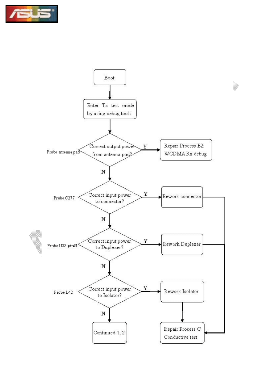
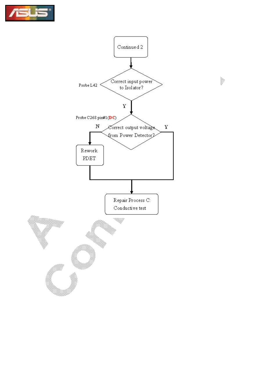
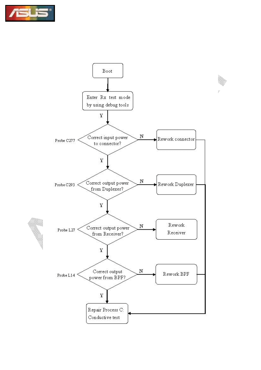
(7) Repair Process E2: WCDMA Rx debug
The flow chart of Repair Process E2 is shown below.

45
The purpose of this repair process is to find out where the problem is on
WCDMA Rx path. In other words, engineers can judge the defect component on RF
path by using “Debug tool” and RF signal generator. Debug tool makes Halley into
test mode and keeps Rx path receiving CW (continuous wave) from the generator.
The usage of debug tool can be referred to “Debug tool user guide” provided by
Halley ATS engineers. Related parameters of debug tool and recommended output
power from the generator are prescribed in the following table.
DL Channel
Rx Frequency
Generator Power
WCDMA
10700
2140.0 MHz
-30 dBm
The detail steps of Repair Process E2 are listed as follows.
a. Set RF signal generator to emit CW with corresponding frequency and
transmit power into Halley WCDMA connector via a RF cable and a RF adapter
(MS-162). Spectrum analyzer connects with a high impedance probe. Execute
WCDMA debug tool and set parameters in the above table.
b. Use the high impedance probe to sequentially measure RF power of test points
on WCDMA Rx path, including C277, C293, L27 and L14. Corresponding locations
are shown in “4. RF Tx/Rx Path and Test Points.” Furthermore, measurement error of
RF power on each test point is unavoidable due to measurement skills and methods of
using high impedance probe.
46
c. C277: Check whether WCDMA RF connector (CON7) is good or not. CON7
needs to be reworked if no RF signal is measured on C277. The following figure is an
example of C277 signal measurement on the spectrum analyzer.
d. C293: Check whether duplexer (U28) is good or not. Duplexer needs to be
reworked if no power is measured on C293. The following figure is an example of
C293 signal measurement on the spectrum analyzer.
47
e. L27: Check whether receiver (U31) is good or not. Receiver needs to be
reworked if no power is measured on L27. The following figure is an example of L27
signal measurement on the spectrum analyzer.
f. L14: Check whether BPF5 is good or not. BPF5 needs to be reworked if no
power is measured on L14. The following figure is an example of L14 signal
measurement on the spectrum analyzer.

48
g. The next process returns to “Repair Process C: GSM/WCDMA conductive
test” after there is no problem in WCDMA Rx path. Moreover, the process returns to
wireless test under the condition of passing conductive test.
Wyszukiwarka
Podobne podstrony:
Electrician's Troubleshooting and Testing Pocket Guide
Herbs for Sports Performance, Energy and Recovery Guide to Optimal Sports Nutrition
4 Steyr Operation and Maintenance Manual 8th edition Feb 08
Optibelt Instalation and maintenance
cinestyle profile user guide v1 Nieznany
03 lubrication and maintenance
Boot Camp Beta Setup Guide v1 4
Money and Happiness A Guide to Living the Good Life
09 Sample Excerpt from Checklist and Audit Guide Rev 1 1 03
Popular Mechanics Suspension Repair And Maintenance
Inspection and maintenance (2)
5 Operation and maintenance manual Alamarin jet Ver 1
Production and Maintenance
JW Player Embedding and JavaScript Guide (1)
Herbs for Sports Performance, Energy and Recovery Guide to Optimal Sports Nutrition
4 Steyr Operation and Maintenance Manual 8th edition Feb 08
AL MAB Separator The practical maintenance guide
Volkswagen Bora 1999, Bora Variant 1999, CC 2010, Eos 2006, Scirocco 200, Golf 1998 and more Guide
Smart Box NVR Series Quick Start Guide V1 0 0
więcej podobnych podstron