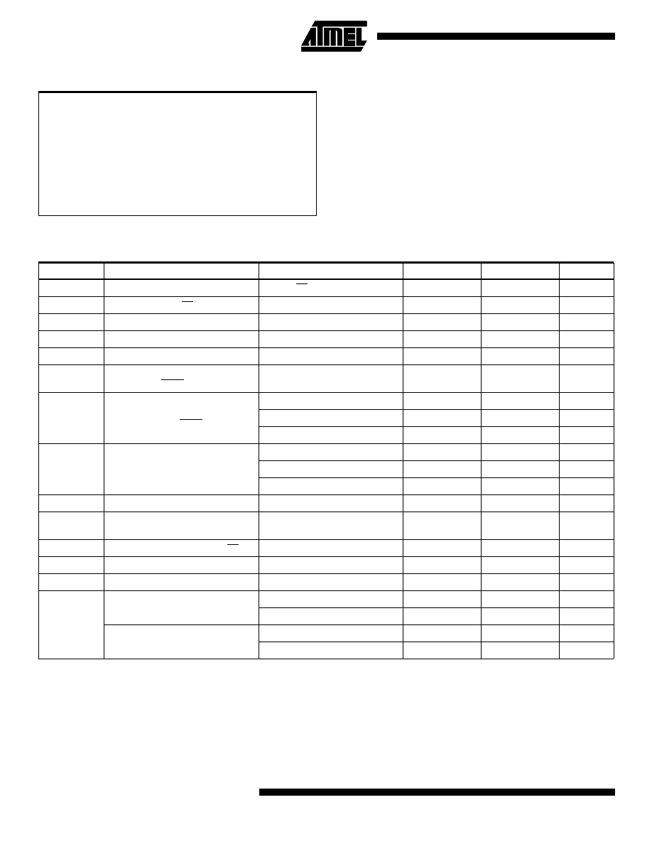
1
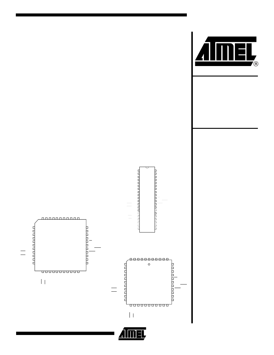
PQFP/TQFP
1
2
3
4
5
6
7
8
9
10
11
33
32
31
30
29
28
27
26
25
24
23
P1.5
P1.6
P1.7
RST
(RXD) P3.0
NC
(TXD) P3.1
(INT0) P3.2
(INT1) P3.3
(T0) P3.4
(T1) P3.5
PO.4 (AD4)
P0.5 (AD5)
P0.6 (AD6)
P0.7 (AD7)
EA/VPP
NC
ALE/PROG
PSEN
P2.7 (A15)
P2.6 (A14)
P2.5 (A13)
44
43
42
41
40
39
38
37
36
35
34
12
13
14
15
16
17
18
19
20
21
22
(WR)P3.6
(RD) P3.7
XTAL2
XTAL1
GND
GND
(A8) P2.0
(A9) P2.1
(A10) P2.2
(A11) P2.3
(A12) P2.4
P1.4
P1.3
P1.2
P1.1 (T2 EX)
P1.0 (T2)
NC
VCC
P0.0 (AD0)
P0.1 (AD1)
P0.2 (AD2)
P0.3 (AD3)
Features
•
Compatible with MCS-51
™
Products
•
4K Bytes of In-System Reprogrammable Flash Memory
– Endurance: 1,000 Write/Erase Cycles
•
Fully Static Operation: 0 Hz to 24 MHz
•
Three-level Program Memory Lock
•
128 x 8-bit Internal RAM
•
32 Programmable I/O Lines
•
Two 16-bit Timer/Counters
•
Six Interrupt Sources
•
Programmable Serial Channel
•
Low-power Idle and Power-down Modes
Description
The AT89C51 is a low-power, high-performance CMOS 8-bit microcomputer with 4K
bytes of Flash programmable and erasable read only memory (PEROM). The device
is manufactured using Atmel’s high-density nonvolatile memory technology and is
compatible with the industry-standard MCS-51 instruction set and pinout. The on-chip
Flash allows the program memory to be reprogrammed in-system or by a conven-
tional nonvolatile memory programmer. By combining a versatile 8-bit CPU with Flash
on a monolithic chip, the Atmel AT89C51 is a powerful microcomputer which provides
a highly-flexible and cost-effective solution to many embedded control applications.
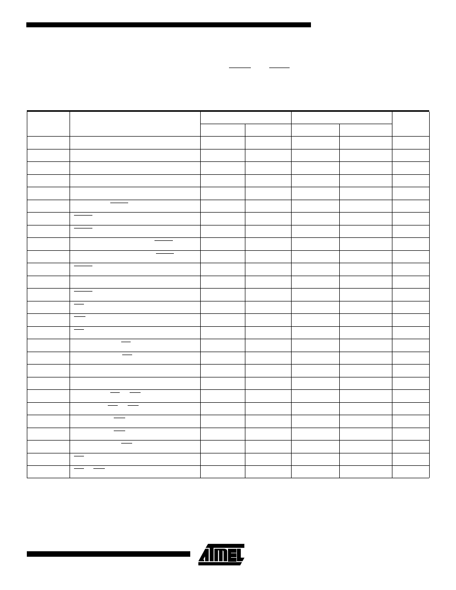
PDIP
1
2
3
4
5
6
7
8
9
10
11
12
13
14
15
16
17
18
19
20
40
39
38
37
36
35
34
33
32
31
30
29
28
27
26
25
24
23
22
21
P1.0
P1.1
P1.2
P1.3
P1.4
P1.5
P1.6
P1.7
RST
(RXD) P3.0
(TXD) P3.1
(INT0) P3.2
(INT1) P3.3
(T0) P3.4
(T1) P3.5
(WR) P3.6
(RD) P3.7
XTAL2
XTAL1
GND
VCC
P0.0 (AD0)
P0.1 (AD1)
P0.2 (AD2)
P0.3 (AD3)
P0.4 (AD4)
P0.5 (AD5)
P0.6 (AD6)
P0.7 (AD7)
EA/VPP
ALE/PROG
PSEN
P2.7 (A15)
P2.6 (A14)
P2.5 (A13)
P2.4 (A12)
P2.3 (A11)
P2.2 (A10)
P2.1 (A9)
P2.0 (A8)
Rev. 0265G–02/00
8-bit
Microcontroller
with 4K Bytes
Flash
AT89C51
Not Recommended
for New Designs.
Use AT89S51.
Pin Configurations
PLCC
7
8
9
10
11
12
13
14
15
16
17
39
38
37
36
35
34
33
32
31
30
29
P1.5
P1.6
P1.7
RST
(RXD) P3.0
NC
(TXD) P3.1
(INT0) P3.2
(INT1) P3.3
(T0) P3.4
(T1) P3.5
PO.4 (AD4)
P0.5 (AD5)
P0.6 (AD6)
P0.7 (AD7)
EA/VPP
NC
ALE/PROG
PSEN
P2.7 (A15)
P2.6 (A14)
P2.5 (A13)
6
5
4
3
2
1
44
43
42
41
40
18
19
20
21
22
23
24
25
26
27
28
(WR)P3.6
(RD) P3.7
XTAL2
XTAL1
GND
NC
(A8) P2.0
(A9) P2.1
(A10) P2.2
(A11) P2.3
(A12) P2.4
P1.4
P1.3
P1.2
P1.1
P1.0
NC
VCC
P0.0 (AD0)
P0.1 (AD1)
P0.2 (AD2)
P0.3 (AD3)
AT89C51
2
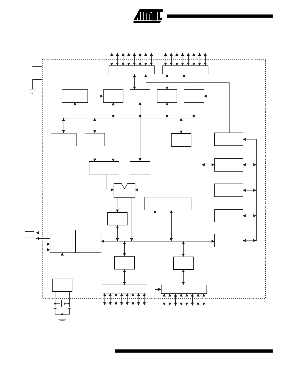
Block Diagram
PORT 2 DRIVERS
PORT 2
LATCH
P2.0 - P2.7
FLASH
PORT 0
LATCH
RAM
PROGRAM
ADDRESS
REGISTER
BUFFER
PC
INCREMENTER
PROGRAM
COUNTER
DPTR
RAM ADDR.
REGISTER
INSTRUCTION
REGISTER
B
REGISTER
INTERRUPT, SERIAL PORT,
AND TIMER BLOCKS
STACK
POINTER
ACC
TMP2
TMP1
ALU
PSW
TIMING
AND
CONTROL
PORT 3
LATCH
PORT 3 DRIVERS
P3.0 - P3.7
PORT 1
LATCH
PORT 1 DRIVERS
P1.0 - P1.7
OSC
GND
V
CC
PSEN
ALE/PROG
EA / V
PP
RST
PORT 0 DRIVERS
P0.0 - P0.7
AT89C51
3
The AT89C51 provides the following standard features: 4K
bytes of Flash, 128 bytes of RAM, 32 I/O lines, two 16-bit
timer/counters, a five vector two-level interrupt architecture,
a full duplex serial port, on-chip oscillator and clock cir-
cuitry. In addition, the AT89C51 is designed with static logic
for operation down to zero frequency and supports two
software selectable power saving modes. The Idle Mode
stops the CPU while allowing the RAM, timer/counters,
serial port and interrupt system to continue functioning. The
Power-down Mode saves the RAM contents but freezes
the oscillator disabling all other chip functions until the next
hardware reset.
Pin Description
VCC
Supply voltage.
GND
Ground.
Port 0
Port 0 is an 8-bit open-drain bi-directional I/O port. As an
output port, each pin can sink eight TTL inputs. When 1s
are written to port 0 pins, the pins can be used as high-
impedance inputs.
Port 0 may also be configured to be the multiplexed low-
order address/data bus during accesses to external pro-
gram and data memory. In this mode P0 has internal
pullups.
Port 0 also receives the code bytes during Flash program-
m i ng , a nd o u tp u t s th e c o d e b y t e s du rin g p ro g ra m
verification. External pullups are required during program
verification.
Port 1
Port 1 is an 8-bit bi-directional I/O port with internal pullups.
The Port 1 output buffers can sink/source four TTL inputs.
When 1s are written to Port 1 pins they are pulled high by
the internal pullups and can be used as inputs. As inputs,
Port 1 pins that are externally being pulled low will source
current (I
IL
) because of the internal pullups.
Port 1 also receives the low-order address bytes during
Flash programming and verification.
Port 2
Port 2 is an 8-bit bi-directional I/O port with internal pullups.
The Port 2 output buffers can sink/source four TTL inputs.
When 1s are written to Port 2 pins they are pulled high by
the internal pullups and can be used as inputs. As inputs,
Port 2 pins that are externally being pulled low will source
current (I
IL
) because of the internal pullups.
Port 2 emits the high-order address byte during fetches
from external program memory and during accesses to
external data memory that use 16-bit addresses (MOVX @
DPTR). In this application, it uses strong internal pullups
when emitting 1s. During accesses to external data mem-
ory that use 8-bit addresses (MOVX @ RI), Port 2 emits the
contents of the P2 Special Function Register.
Port 2 also receives the high-order address bits and some
control signals during Flash programming and verification.
Port 3
Port 3 is an 8-bit bi-directional I/O port with internal pullups.
The Port 3 output buffers can sink/source four TTL inputs.
When 1s are written to Port 3 pins they are pulled high by
the internal pullups and can be used as inputs. As inputs,
Port 3 pins that are externally being pulled low will source
current (I
IL
) because of the pullups.
Port 3 also serves the functions of various special features
of the AT89C51 as listed below:
Port 3 also receives some control signals for Flash pro-
gramming and verification.
RST
Reset input. A high on this pin for two machine cycles while
the oscillator is running resets the device.
ALE/PROG
Address Latch Enable output pulse for latching the low byte
of the address during accesses to external memory. This
pin is also the program pulse input (PROG) during Flash
programming.
In normal operation ALE is emitted at a constant rate of 1/6
the oscillator frequency, and may be used for external tim-
ing or clocking purposes. Note, however, that one ALE
Port Pin
Alternate Functions
P3.0
RXD (serial input port)
P3.1
TXD (serial output port)
P3.2
INT0 (external interrupt 0)
P3.3
INT1 (external interrupt 1)
P3.4
T0 (timer 0 external input)
P3.5
T1 (timer 1 external input)
P3.6
WR (external data memory write strobe)
P3.7
RD (external data memory read strobe)
AT89C51
4
pulse is skipped during each access to external Data
Memory.
If desired, ALE operation can be disabled by setting bit 0 of
SFR location 8EH. With the bit set, ALE is active only dur-
ing a MOVX or MOVC instruction. Otherwise, the pin is
weakly pulled high. Setting the ALE-disable bit has no
effect if the microcontroller is in external execution mode.
PSEN
Program Store Enable is the read strobe to external pro-
gram memory.
When the AT89C51 is executing code from external pro-
gram memory, PSEN is activated twice each machine
cycle, except that two PSEN activations are skipped during
each access to external data memory.
EA/VPP
External Access Enable. EA must be strapped to GND in
order to enable the device to fetch code from external pro-
gram memory locations starting at 0000H up to FFFFH.
Note, however, that if lock bit 1 is programmed, EA will be
internally latched on reset.
EA should be strapped to V
C C
for internal program
executions.
This pin also receives the 12-volt programming enable volt-
age (V
PP
) during Flash programming, for parts that require
12-volt V
PP
.
XTAL1
Input to the inverting oscillator amplifier and input to the
internal clock operating circuit.
XTAL2
Output from the inverting oscillator amplifier.
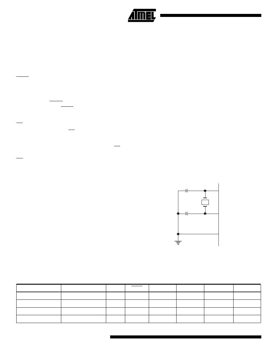
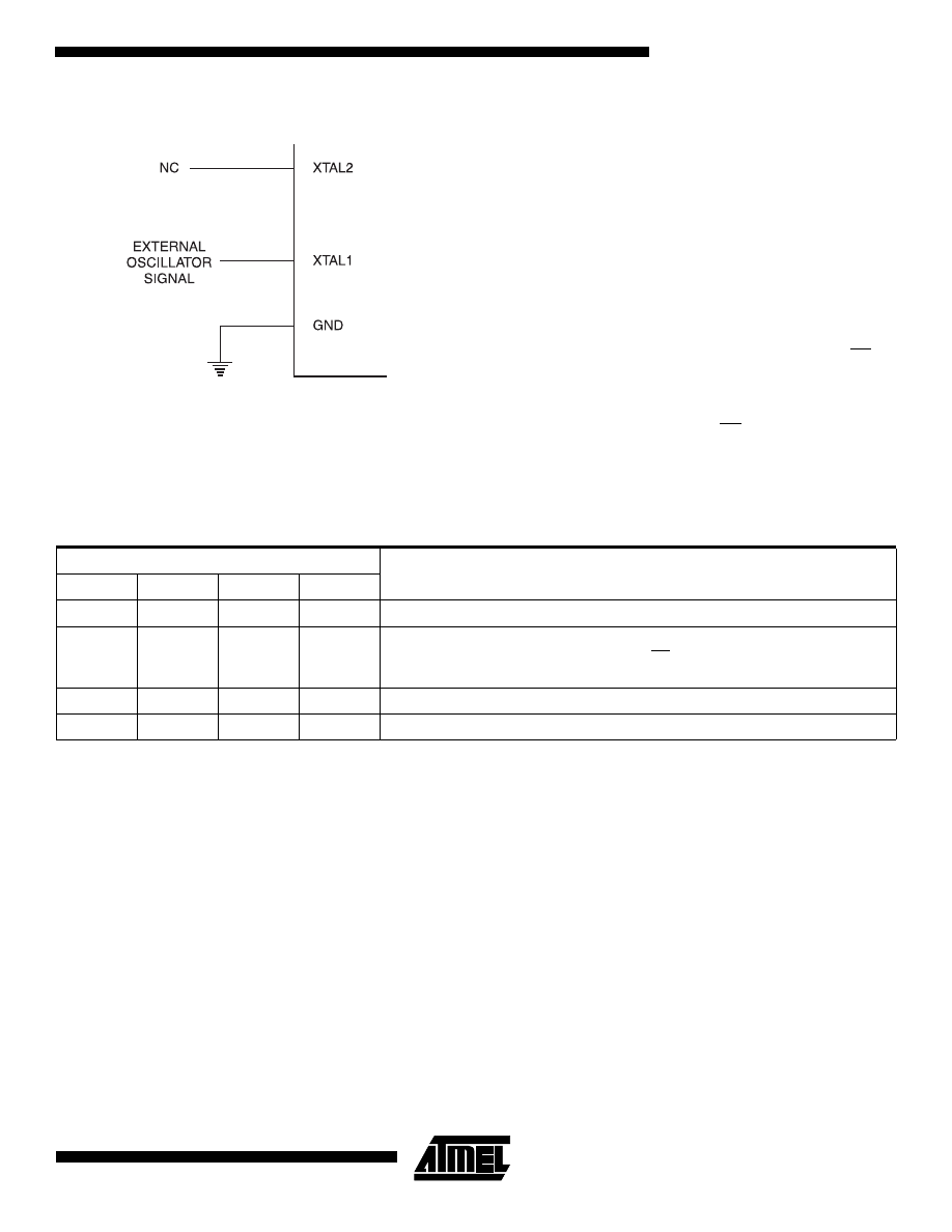
Oscillator Characteristics
XTAL1 and XTAL2 are the input and output, respectively,
of an inverting amplifier which can be configured for use as
an on-chip oscillator, as shown in Figure 1. Either a quartz
crystal or ceramic resonator may be used. To drive the
device from an external clock source, XTAL2 should be left
unconnected while XTAL1 is driven as shown in Figure 2.
There are no requirements on the duty cycle of the external
clock signal, since the input to the internal clocking circuitry
is through a divide-by-two flip-flop, but minimum and maxi-
mum voltage high and low time specifications must be
observed.
Idle Mode
In idle mode, the CPU puts itself to sleep while all the on-
chip peripherals remain active. The mode is invoked by
software. The content of the on-chip RAM and all the spe-
cial functions registers remain unchanged during this
mode. The idle mode can be terminated by any enabled
interrupt or by a hardware reset.
It should be noted that when idle is terminated by a hard
ware reset, the device normally resumes program execu-
tion, from where it left off, up to two machine cycles before
the internal reset algorithm takes control. On-chip hardware
inhibits access to internal RAM in this event, but access to
the port pins is not inhibited. To eliminate the possibility of
an unexpected write to a port pin when Idle is terminated by
reset, the instruction following the one that invokes Idle
should not be one that writes to a port pin or to external
memory.
Figure 1. Oscillator Connections
Note:
C1, C2 = 30 pF
±
10 pF for Crystals
= 40 pF
±
10 pF for Ceramic Resonators
C2
XTAL2
GND
XTAL1
C1
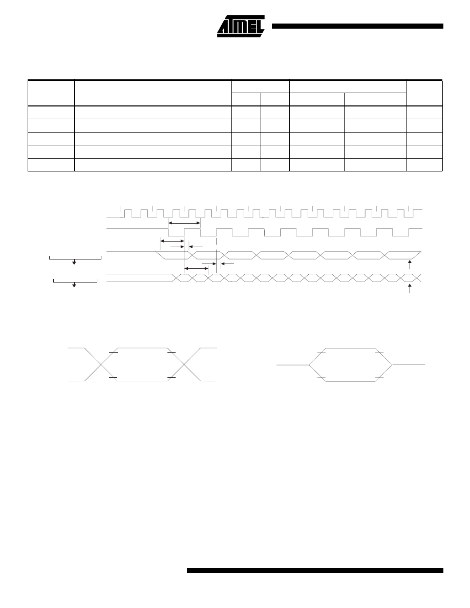
Status of External Pins During Idle and Power-down Modes
Mode
Program Memory
ALE
PSEN
PORT0
PORT1
PORT2
PORT3
Idle
Internal
1
1
Data
Data
Data
Data
Idle
External
1
1
Float
Data
Address
Data
Power-down
Internal
0
0
Data
Data
Data
Data
Power-down
External
0
0
Float
Data
Data
Data
AT89C51
5
Figure 2. External Clock Drive Configuration
Power-down Mode
In the power-down mode, the oscillator is stopped, and the
instruction that invokes power-down is the last instruction
executed. The on-chip RAM and Special Function Regis-
ters retain their values until the power-down mode is
terminated. The only exit from power-down is a hardware
reset. Reset redefines the SFRs but does not change the
on-chip RAM. The reset should not be activated before V
CC
is restored to its normal operating level and must be held
active long enough to allow the oscillator to restart and
stabilize.
Program Memory Lock Bits
On the chip are three lock bits which can be left unpro-
grammed (U) or can be programmed (P) to obtain the
additional features listed in the table below.
When lock bit 1 is programmed, the logic level at the EA pin
is sampled and latched during reset. If the device is pow-
ered up without a reset, the latch initializes to a random
value, and holds that value until reset is activated. It is nec-
essary that the latched value of EA be in agreement with
the current logic level at that pin in order for the device to
function properly.
Lock Bit Protection Modes
Program Lock Bits
Protection Type
LB1
LB2
LB3
1
U
U
U
No program lock features
2
P
U
U
MOVC instructions executed from external program memory are disabled from
fetching code bytes from internal memory, EA is sampled and latched on reset,
and further programming of the Flash is disabled
3
P
P
U
Same as mode 2, also verify is disabled
4
P
P
P
Same as mode 3, also external execution is disabled

AT89C51
6
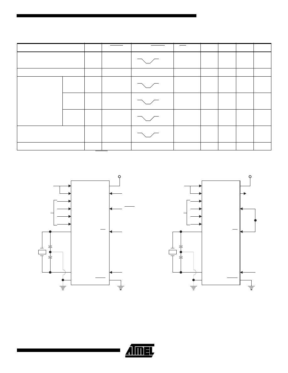
Programming the Flash
The AT89C51 is normally shipped with the on-chip Flash
memory array in the erased state (that is, contents = FFH)
and ready to be programmed. The programming interface
accepts either a high-voltage (12-volt) or a low-voltage
(V
CC
) program enable signal. The low-voltage program-
ming mode provides a convenient way to program the
AT89C51 inside the user’s system, while the high-voltage
programming mode is compatible with conventional third-
party Flash or EPROM programmers.
The AT89C51 is shipped with either the high-voltage or
low-voltage programming mode enabled. The respective
top-side marking and device signature codes are listed in
the following table.
The AT89C51 code memory array is programmed byte-by-
byte in either programming mode. To program any non-
blank byte in the on-chip Flash Memory, the entire memory
must be erased using the Chip Erase Mode.
Programming Algorithm: Before programming the
AT89C51, the address, data and control signals should be
set up according to the Flash programming mode table and
Figure 3 and Figure 4. To program the AT89C51, take the
following steps.
1.
Input the desired memory location on the address
lines.
2.
Input the appropriate data byte on the data lines.
3.
Activate the correct combination of control signals.
4.
Raise EA/V
PP
to 12V for the high-voltage program-
ming mode.
5.
Pulse ALE/PROG once to program a byte in the
Flash array or the lock bits. The byte-write cycle is
self-timed and typically takes no more than 1.5 ms.
Repeat steps 1 through 5, changing the address
and data for the entire array or until the end of the
object file is reached.
Data Polling: The AT89C51 features Data Polling to indi-
cate the end of a write cycle. During a write cycle, an
attempted read of the last byte written will result in the com-
plement of the written datum on PO.7. Once the write cycle
has been completed, true data are valid on all outputs, and
the next cycle may begin. Data Polling may begin any time
after a write cycle has been initiated.
Ready/Busy: The progress of byte programming can also
be monitored by the RDY/BSY output signal. P3.4 is pulled
low after ALE goes high during programming to indicate
BUSY. P3.4 is pulled high again when programming is
done to indicate READY.
Program Verify: If lock bits LB1 and LB2 have not been
programmed, the programmed code data can be read back
via the address and data lines for verification. The lock bits
cannot be verified directly. Verification of the lock bits is
achieved by observing that their features are enabled.
Chip Erase: The entire Flash array is erased electrically
by using the proper combination of control signals and by
holding ALE/PROG low for 10 ms. The code array is written
with all “1”s. The chip erase operation must be executed
before the code memory can be re-programmed.
Reading the Signature Bytes: The signature bytes are
read by the same procedure as a normal verification of
locations 030H, 031H, and 032H, except that P3.6 and
P3.7 must be pulled to a logic low. The values returned are
as follows.
(030H) = 1EH indicates manufactured by Atmel
(031H) = 51H indicates 89C51
(032H) = FFH indicates 12V programming
(032H) = 05H indicates 5V programming
Programming Interface
Every code byte in the Flash array can be written and the
entire array can be erased by using the appropriate combi-
nation of control signals. The write operation cycle is self-
timed and once initiated, will automatically time itself to
completion.
All major programming vendors offer worldwide support for
the Atmel microcontroller series. Please contact your local
programming vendor for the appropriate software revision.
V
PP
= 12V
V
PP
= 5V
Top-side Mark
AT89C51
xxxx
yyww
AT89C51
xxxx-5
yyww
Signature
(030H) = 1EH
(031H) = 51H
(032H) =F FH
(030H) = 1EH
(031H) = 51H
(032H) = 05H
AT89C51
7
Note:
1. Chip Erase requires a 10 ms PROG pulse.
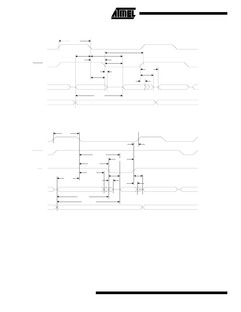
Figure 3. Programming the Flash
Figure 4. Verifying the Flash
Flash Programming Modes
Mode
RST
PSEN
ALE/PROG
EA/V
PP
P2.6
P2.7
P3.6
P3.7
Write Code Data
H
L
H/12V
L
H
H
H
Read Code Data
H
L
H
H
L
L
H
H
Write Lock
Bit - 1
H
L
H/12V
H
H
H
H
Bit - 2
H
L
H/12V
H
H
L
L
Bit - 3
H
L
H/12V
H
L
H
L
Chip Erase
H
L
H/12V
H
L
L
L
Read Signature Byte
H
L
H
H
L
L
L
L
(1)
P1
P2.6
P3.6
P2.0 - P2.3
A0 - A7
ADDR.
OOOOH/OFFFH
T
SEE FLASH
PROGRAMMING
MODES
ABLE
3-24 MHz
A8 - A11
P0
+5V
P2.7
PGM
DATA
PROG
V /V
IH
PP
V
IH
ALE
P3.7
XTAL2
EA
RST
PSEN
XTAL1
GND
V
CC
AT89C51
P1
P2.6
P3.6
P2.0 - P2.3
A0 - A7
ADDR.
OOOOH/0FFFH
3-24 MHz
A8 - A11
P0
+5V
P2.7
PGM DATA
(USE 10K
PULLUPS)
V
IH
V
IH
ALE
P3.7
XTAL2
EA
RST
PSEN
XTAL1
GND
V
CC
AT89C51
T
SEE FLASH
PROGRAMMING
MODES
ABLE
AT89C51
8
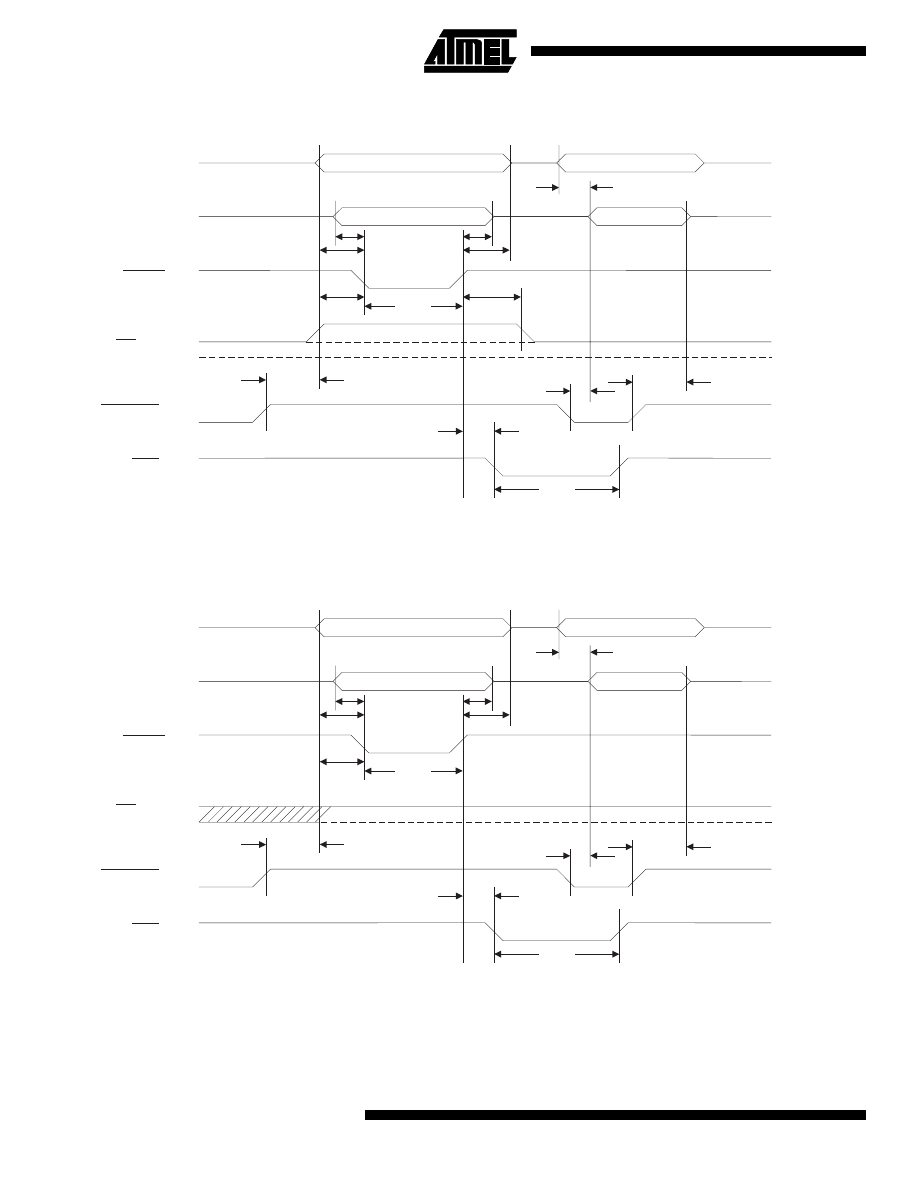
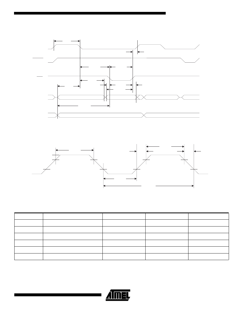
Flash Programming and Verification Waveforms - High-voltage Mode (V
PP
= 12V)
Flash Programming and Verification Waveforms - Low-voltage Mode (V
PP
= 5V)
t
GLGH
t
GHSL
t
AVGL
t
SHGL
t
DVGL
t
GHAX
t
AVQV
t
GHDX
t
EHSH
t
ELQV
t
WC
BUSY
READY
t
GHBL
t
EHQZ
P1.0 - P1.7
P2.0 - P2.3
ALE/PROG
PORT 0
LOGIC 1
LOGIC 0
EA/V
PP
V
PP
P2.7
(ENABLE)
P3.4
(RDY/BSY)
PROGRAMMING
ADDRESS
VERIFICATION
ADDRESS
DATA IN
DATA OUT
t
GLGH
t
AVGL
t
SHGL
t
DVGL
t
GHAX
t
AVQV
t
GHDX
t
EHSH
t
ELQV
t
WC
BUSY
READY
t
GHBL
t
EHQZ
P1.0 - P1.7
P2.0 - P2.3
ALE/PROG
PORT 0
LOGIC 1
LOGIC 0
EA/V
PP
P2.7
(ENABLE)
P3.4
(RDY/BSY)
PROGRAMMING
ADDRESS
VERIFICATION
ADDRESS
DATA IN
DATA OUT
AT89C51
9
Note:
1. Only used in 12-volt programming mode.
Flash Programming and Verification Characteristics
T
A
= 0°C to 70°C, V
CC
= 5.0
±
10%
Symbol
Parameter
Min
Max
Units
V
PP
(1)
Programming Enable Voltage
11.5
12.5
V
I
PP
(1)
Programming Enable Current
1.0
mA
1/t
CLCL
Oscillator Frequency
3
24
MHz
t
AVGL
Address Setup to PROG Low
48t
CLCL
t
GHAX
Address Hold after PROG
48t
CLCL
t
DVGL
Data Setup to PROG Low
48t
CLCL
t
GHDX
Data Hold after PROG
48t
CLCL
t
EHSH
P2.7 (ENABLE) High to V
PP
48t
CLCL
t
SHGL
V
PP
Setup to PROG Low
10
µs
t
GHSL
(1)
V
PP
Hold after PROG
10
µs
t
GLGH
PROG Width
1
110
µs
t
AVQV
Address to Data Valid
48t
CLCL
t
ELQV
ENABLE Low to Data Valid
48t
CLCL
t
EHQZ
Data Float after ENABLE
0
48t
CLCL
t
GHBL
PROG High to BUSY Low
1.0
µs
t
WC
Byte Write Cycle Time
2.0
ms
AT89C51
10
Absolute Maximum Ratings*
Notes:
1. Under steady state (non-transient) conditions, I
OL
must be externally limited as follows:
Maximum I
OL
per port pin: 10 mA
Maximum I
OL
per 8-bit port: Port 0: 26 mA
Ports 1, 2, 3: 15 mA
Maximum total I
OL
for all output pins: 71 mA
If I
OL
exceeds the test condition, V
OL
may exceed the related specification. Pins are not guaranteed to sink current greater
than the listed test conditions.
2. Minimum V
CC
for Power-down is 2V.
Operating Temperature.................................. -55°C to +125°C
*NOTICE:
Stresses beyond those listed under “Absolute
Maximum Ratings” may cause permanent dam-
age to the device. This is a stress rating only and
functional operation of the device at these or any
other conditions beyond those indicated in the
operational sections of this specification is not
implied. Exposure to absolute maximum rating
conditions for extended periods may affect device
reliability.
Storage Temperature ..................................... -65°C to +150°C
Voltage on Any Pin
with Respect to Ground .....................................-1.0V to +7.0V
Maximum Operating Voltage ............................................ 6.6V
DC Output Current...................................................... 15.0 mA
DC Characteristics
T
A
= -40°C to 85°C, V
CC
= 5.0V
±
20% (unless otherwise noted)
Symbol
Parameter
Condition
Min
Max
Units
V
IL
Input Low-voltage
(Except EA)
-0.5
0.2 V
CC
- 0.1
V
V
IL1
Input Low-voltage (EA)
-0.5
0.2 V
CC
- 0.3
V
V
IH
Input High-voltage
(Except XTAL1, RST)
0.2 V
CC
+ 0.9
V
CC
+ 0.5
V
V
IH1
Input High-voltage
(XTAL1, RST)
0.7 V
CC
V
CC
+ 0.5
V
V
OL
Output Low-voltage
(1)
(Ports 1,2,3)
I
OL
= 1.6 mA
0.45
V
V
OL1
Output Low-voltage
(1)
(Port 0, ALE, PSEN)
I
OL
= 3.2 mA
0.45
V
V
OH
Output High-voltage
(Ports 1,2,3, ALE, PSEN)
I
OH
= -60 µA, V
CC
= 5V
±
10%
2.4
V
I
OH
= -25 µA
0.75 V
CC
V
I
OH
= -10 µA
0.9 V
CC
V
V
OH1
Output High-voltage
(Port 0 in External Bus Mode)
I
OH
= -800 µA, V
CC
= 5V
±
10%
2.4
V
I
OH
= -300
µ
A
0.75 V
CC
V
I
OH
= -80
µ
A
0.9 V
CC
V
I
IL
Logical 0 Input Current (Ports 1,2,3)
V
IN
= 0.45V
-50
µ
A
I
TL
Logical 1 to 0 Transition Current
(Ports 1,2,3)
V
IN
= 2V, VCC = 5V
±
10%
-650
µ
A
I
LI
Input Leakage Current (Port 0, EA)
0.45 < V
IN
< V
CC
±
10
µ
A
RRST
Reset Pull-down Resistor
50
300
K
Ω
C
IO
Pin Capacitance
Test Freq. = 1 MHz, T
A
= 25°C
10
pF
I
CC
Power Supply Current
Active Mode, 12 MHz
20
mA
Idle Mode, 12 MHz
5
mA
Power-down Mode
(2)
V
CC
= 6V
100
µ
A
V
CC
= 3V
40
µ
A
AT89C51
11
AC Characteristics
Under operating conditions, load capacitance for Port 0, ALE/PROG, and PSEN = 100 pF; load capacitance for all other
outputs = 80 pF.
External Program and Data Memory Characteristics
Symbol
Parameter
12 MHz Oscillator
16 to 24 MHz Oscillator
Units
Min
Max
Min
Max
1/t
CLCL
Oscillator Frequency
0
24
MHz
t
LHLL
ALE Pulse Width
127
2t
CLCL
-40
ns
t
AVLL
Address Valid to ALE Low
43
t
CLCL
-13
ns
t
LLAX
Address Hold after ALE Low
48
t
CLCL
-20
ns
t
LLIV
ALE Low to Valid Instruction In
233
4t
CLCL
-65
ns
t
LLPL
ALE Low to PSEN Low
43
t
CLCL
-13
ns
t
PLPH
PSEN Pulse Width
205
3t
CLCL
-20
ns
t
PLIV
PSEN Low to Valid Instruction In
145
3t
CLCL
-45
ns
t
PXIX
Input Instruction Hold after PSEN
0
0
ns
t
PXIZ
Input Instruction Float after PSEN
59
t
CLCL
-10
ns
t
PXAV
PSEN to Address Valid
75
t
CLCL
-8
ns
t
AVIV
Address to Valid Instruction In
312
5t
CLCL
-55
ns
t
PLAZ
PSEN Low to Address Float
10
10
ns
t
RLRH
RD Pulse Width
400
6t
CLCL
-100
ns
t
WLWH
WR Pulse Width
400
6t
CLCL
-100
ns
t
RLDV
RD Low to Valid Data In
252
5t
CLCL
-90
ns
t
RHDX
Data Hold after RD
0
0
ns
t
RHDZ
Data Float after RD
97
2t
CLCL
-28
ns
t
LLDV
ALE Low to Valid Data In
517
8t
CLCL
-150
ns
t
AVDV
Address to Valid Data In
585
9t
CLCL
-165
ns
t
LLWL
ALE Low to RD or WR Low
200
300
3t
CLCL
-50
3t
CLCL
+50
ns
t
AVWL
Address to RD or WR Low
203
4t
CLCL
-75
ns
t
QVWX
Data Valid to WR Transition
23
t
CLCL
-20
ns
t
QVWH
Data Valid to WR High
433
7t
CLCL
-120
ns
t
WHQX
Data Hold after WR
33
t
CLCL
-20
ns
t
RLAZ
RD Low to Address Float
0
0
ns
t
WHLH
RD or WR High to ALE High
43
123
t
CLCL
-20
t
CLCL
+25
ns
AT89C51
12
External Program Memory Read Cycle
External Data Memory Read Cycle
t
LHLL
t
LLIV
t
PLIV
t
LLAX
t
PXIZ
t
PLPH
t
PLAZ
t
PXAV
t
AVLL
t
LLPL
t
AVIV
t
PXIX
ALE
PSEN
PORT 0
PORT 2
A8 - A15
A0 - A7
A0 - A7
A8 - A15
INSTR IN
t
LHLL
t
LLDV
t
LLWL
t
LLAX
t
WHLH
t
AVLL
t
RLRH
t
AVDV
t
AVWL
t
RLAZ
t
RHDX
t
RLDV
t
RHDZ
A0 - A7 FROM RI OR DPL
ALE
PSEN
RD
PORT 0
PORT 2
P2.0 - P2.7 OR A8 - A15 FROM DPH
A0 - A7 FROM PCL
A8 - A15 FROM PCH
DATA IN
INSTR IN
AT89C51
13
External Data Memory Write Cycle
External Clock Drive Waveforms
External Clock Drive
Symbol
Parameter
Min
Max
Units
1/t
CLCL
Oscillator Frequency
0
24
MHz
t
CLCL
Clock Period
41.6
ns
t
CHCX
High Time
15
ns
t
CLCX
Low Time
15
ns
t
CLCH
Rise Time
20
ns
t
CHCL
Fall Time
20
ns
t
LHLL
t
LLWL
t
LLAX
t
WHLH
t
AVLL
t
WLWH
t
AVWL
t
QVWX
t
QVWH
t
WHQX
A0 - A7 FROM RI OR DPL
ALE
PSEN
WR
PORT 0
PORT 2
P2.0 - P2.7 OR A8 - A15 FROM DPH
A0 - A7 FROM PCL
A8 - A15 FROM PCH
DATA OUT
INSTR IN
t
CHCX
t
CHCX
t
CLCX
t
CLCL
t
CHCL
t
CLCH
V - 0.5V
CC
0.45V
0.2 V
- 0.1V
CC
0.7 V
CC
AT89C51
14
Shift Register Mode Timing Waveforms
AC Testing Input/Output Waveforms
(1)
Note:
1. AC Inputs during testing are driven at V
CC
- 0.5V for a
logic 1 and 0.45V for a logic 0. Timing measurements
are made at V
IH
min. for a logic 1 and V
IL
max. for a
logic 0.
Float Waveforms
(1)
Note:
1. For timing purposes, a port pin is no longer floating
when a 100 mV change from load voltage occurs. A
port pin begins to float when 100 mV change from
the loaded V
OH
/V
OL
level occurs.
Serial Port Timing: Shift Register Mode Test Conditions
(V
CC
= 5.0 V
±
20%; Load Capacitance = 80 pF)
Symbol
Parameter
12 MHz Osc
Variable Oscillator
Units
Min
Max
Min
Max
t
XLXL
Serial Port Clock Cycle Time
1.0
12t
CLCL
µs
t
QVXH
Output Data Setup to Clock Rising Edge
700
10t
CLCL
-133
ns
t
XHQX
Output Data Hold after Clock Rising Edge
50
2t
CLCL
-117
ns
t
XHDX
Input Data Hold after Clock Rising Edge
0
0
ns
t
XHDV
Clock Rising Edge to Input Data Valid
700
10t
CLCL
-133
ns
t
XHDV
t
QVXH
t
XLXL
t
XHDX
t
XHQX
ALE
INPUT DATA
CLEAR RI
OUTPUT DATA
WRITE TO SBUF
INSTRUCTION
CLOCK
0
0
1
1
2
2
3
3
4
4
5
5
6
6
7
7
SET TI
SET RI
8
VALID
VALID
VALID
VALID
VALID
VALID
VALID
VALID
0.45V
TEST POINTS
V - 0.5V
CC
0.2 V + 0.9V
CC
0.2 V - 0.1V
CC
V
LOAD
+ 0.1V
Timing Reference
Points
V
LOAD
- 0.1V
LOAD
V
V
OL
+ 0.1V
V
OL
- 0.1V

AT89C51
15
Ordering Information
Speed
(MHz)
Power
Supply
Ordering Code
Package
Operation Range
12
5V
±
20%
AT89C51-12AC
44A
Commercial
AT89C51-12JC
44J
(0
°
C to 70
°
C)
AT89C51-12PC
40P6
AT89C51-12QC
44Q
AT89C51-12AI
44A
Industrial
AT89C51-12JI
44J
(-40
°
C to 85
°
C)
AT89C51-12PI
40P6
AT89C51-12QI
44Q
16
5V
±
20%
AT89C51-16AC
44A
Commercial
AT89C51-16JC
44J
(0
°
C to 70
°
C)
AT89C51-16PC
40P6
AT89C51-16QC
44Q
AT89C51-16AI
44A
Industrial
AT89C51-16JI
44J
(-40
°
C to 85
°
C)
AT89C51-16PI
40P6
AT89C51-16QI
44Q
20
5V
±
20%
AT89C51-20AC
44A
Commercial
AT89C51-20JC
44J
(0
°
C to 70
°
C)
AT89C51-20PC
40P6
AT89C51-20QC
44Q
AT89C51-20AI
44A
Industrial
AT89C51-20JI
44J
(-40
°
C to 85
°
C)
AT89C51-20PI
40P6
AT89C51-20QI
44Q
24
5V
±
20%
AT89C51-24AC
44A
Commercial
AT89C51-24JC
44J
(0
°
C to 70
°
C)
AT89C51-24PC
40P6
AT89C51-24QC
44Q
AT89C51-24AI
44A
Industrial
AT89C51-24JI
44J
(-40
°
C to 85
°
C)
AT89C51-24PI
40P6
AT89C51-24QI
44Q
Package Type
44A
44-lead, Thin Plastic Gull Wing Quad Flatpack (TQFP)
44J
44-lead, Plastic J-leaded Chip Carrier (PLCC)
40P6
40-lead, 0.600” Wide, Plastic Dual Inline Package (PDIP)
44Q
44-lead, Plastic Gull Wing Quad Flatpack (PQFP)
AT89C51
16
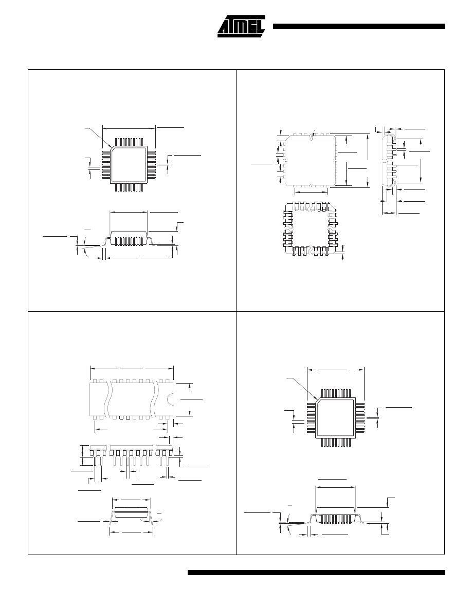
Packaging Information
Controlling dimension: millimeters
1.20(0.047) MAX
10.10(0.394)
9.90(0.386)
SQ
12.21(0.478)
11.75(0.458)
SQ
0.75(0.030)
0.45(0.018)
0.15(0.006)
0.05(0.002)
0.20(.008)
0.09(.003)
0
7
0.80(0.031) BSC
PIN 1 ID
0.45(0.018)
0.30(0.012)
.045(1.14) X 45°
PIN NO. 1
IDENTIFY
.045(1.14) X 30° - 45°
.012(.305)
.008(.203)
.021(.533)
.013(.330)
.630(16.0)
.590(15.0)
.043(1.09)
.020(.508)
.120(3.05)
.090(2.29)
.180(4.57)
.165(4.19)
.500(12.7) REF SQ
.032(.813)
.026(.660)
.050(1.27) TYP
.022(.559) X 45° MAX (3X)
.656(16.7)
.650(16.5)
.695(17.7)
.685(17.4)
SQ
SQ
2.07(52.6)
2.04(51.8)
PIN
1
.566(14.4)
.530(13.5)
.090(2.29)
MAX
.005(.127)
MIN
.065(1.65)
.015(.381)
.022(.559)
.014(.356)
.065(1.65)
.041(1.04)
0
15
REF
.690(17.5)
.610(15.5)
.630(16.0)
.590(15.0)
.012(.305)
.008(.203)
.110(2.79)
.090(2.29)
.161(4.09)
.125(3.18)
SEATING
PLANE
.220(5.59)
MAX
1.900(48.26) REF
Controlling dimension: millimeters
13.45 (0.525)
12.95 (0.506)
0.50 (0.020)
0.35 (0.014)
SQ
PIN 1 ID
0.80 (0.031) BSC
10.10 (0.394)
9.90 (0.386)
SQ
0
7
0.17 (0.007)
0.13 (0.005)
1.03 (0.041)
0.78 (0.030)
2.45 (0.096) MAX
0.25 (0.010) MAX
44A, 44-lead, Thin (1.0 mm) Plastic Gull Wing Quad
Flatpack (TQFP)
Dimensions in Millimeters and (Inches)*
JEDEC STANDARD MS-026 ACB
44J, 44-lead, Plastic J-leaded Chip Carrier (PLCC)
Dimensions in Inches and (Millimeters)
JEDEC STANDARD MS-018 AC
40P6, 40-lead, 0.600" Wide, Plastic Dual Inline
Package (PDIP)
Dimensions in Inches and (Millimeters)
44Q, 44-lead, Plastic Quad Flat Package (PQFP)
Dimensions in Millimeters and (Inches)*
JEDEC STANDARD MS-022 AB

© Atmel Corporation 2000.
Atmel Corporation makes no warranty for the use of its products, other than those expressly contained in the Company’s standard war-
ranty which is detailed in Atmel’s Terms and Conditions located on the Company’s web site. The Company assumes no responsibility for
any errors which may appear in this document, reserves the right to change devices or specifications detailed herein at any time without
notice, and does not make any commitment to update the information contained herein. No licenses to patents or other intellectual prop-
erty of Atmel are granted by the Company in connection with the sale of Atmel products, expressly or by implication. Atmel’s products are
not authorized for use as critical components in life suppor t devices or systems.
Atmel Headquarters
Atmel Operations
Corporate Headquarters
2325 Orchard Parkway
San Jose, CA 95131
TEL (408) 441-0311
FAX (408) 487-2600
Europe
Atmel U.K., Ltd.
Coliseum Business Centre
Riverside Way
Camberley, Surrey GU15 3YL
England
TEL (44) 1276-686-677
FAX (44) 1276-686-697
Asia
Atmel Asia, Ltd.
Room 1219
Chinachem Golden Plaza
77 Mody Road Tsimhatsui
East Kowloon
Hong Kong
TEL (852) 2721-9778
FAX (852) 2722-1369
Japan
Atmel Japan K.K.
9F, Tonetsu Shinkawa Bldg.
1-24-8 Shinkawa
Chuo-ku, Tokyo 104-0033
Japan
TEL (81) 3-3523-3551
FAX (81) 3-3523-7581
Atmel Colorado Springs
1150 E. Cheyenne Mtn. Blvd.
Colorado Springs, CO 80906
TEL (719) 576-3300
FAX (719) 540-1759
Atmel Rousset
Zone Industrielle
13106 Rousset Cedex
France
TEL (33) 4-4253-6000
FAX (33) 4-4253-6001
Fax-on-Demand
North America:
1-(800) 292-8635
International:
1-(408) 441-0732
literature@atmel.com
Web Site
http://www.atmel.com
BBS
1-(408) 436-4309
Printed on recycled paper.
0265G–02/00/xM
Marks bearing
®
and/or
™
are registered trademarks and trademarks of Atmel Corporation.
Terms and product names in this document may be trademarks of others.
Document Outline
- Block Diagram
- Features
- Description
- Pin Description
- Oscillator Characteristics
- Status of External Pins During Idle and Power-down Modes
- Lock Bit Protection Modes
- Programming the Flash
- Programming Interface
- Flash Programming Modes
- Flash Programming and Verification Waveforms - High-voltage Mode (VPP = 12V)
- Flash Programming and Verification Waveforms - Low-voltage Mode (VPP = 5V)
- Flash Programming and Verification Characteristics
- Absolute Maximum Ratings*
- DC Characteristics
- AC Characteristics
- External Program and Data Memory Characteristics
- External Program Memory Read Cycle
- External Data Memory Read Cycle
- External Data Memory Write Cycle
- External Clock Drive Waveforms
- External Clock Drive
- Serial Port Timing: Shift Register Mode Test Conditions
- Shift Register Mode Timing Waveforms
- AC Testing Input/Output Waveforms(1)
- Float Waveforms(1)
- Ordering Information
Wyszukiwarka
Podobne podstrony:
8 Bit Microcontroller Drives Ba Nieznany (2)
How to build a USB device with PIC 18F4550 or 18F2550 (and the microchip CDC firmware)
Atmel 8271 8 bit AVR Microcontroller ATmega48A 48PA 88A 88PA 168A 168PA 328 328P datasheet Summary
7483 4 BIT BINARY FULL ADDER WITH FAST CARRY
flash or repair Apollo 726 with Tracer OVO firmware and Apollo fix firmware
Controlling DC Brushless Motors with PIC17C756A (Microchip AN718, 1999)
HOW TO FLASH WITH ODIS ENGINEERING
Getting Started with PIC Microcontrollers F Stevens (1997) WW(1)
Image Processing with Matlab 33
L 5590 Short Sleeved Dress With Zipper Closure
M 5190 Long dress with a contrast finishing work
O'Reilly How To Build A FreeBSD STABLE Firewall With IPFILTER From The O'Reilly Anthology
więcej podobnych podstron