
Noise propagation path identification of variable speed drive in time
domain via common mode test mode
D. Zhao*, J.A. Ferreira*, H. Polinder*, A. Roc’h**, and F.B.J. Leferink**
,
***
*Delft University of Technology, Mekelweg 4, 2628CD, Delft, The Netherlands
**University of Twente, Enschede, P.O. Box 217, 7500 AE Enschede,,The Netherlands
*** Thales Netherlands, Henglo, P.O. Box 42, 7550 GD Hengelo, The Netherlands
E-Mail: d.zhao@ewi.tudelft.nl
Acknowledgements
This work is an IOP (Innovative Research Project) project financed by the Dutch Ministry of
Economic Affairs.
Keywords
EMC/EMI, variable speed drive, voltage source inverter
Abstract
Electromagnetic Compatibility (EMC) debugging of power electronics systems depends heavily on the
experience of specialists due to the complex mechanisms of electromagnetic noise. In this paper, the
time domain approach is used instead of the conventional frequency domain method to identify noise
propagation path. The proposed test mode switches the upper or lower transistors of the converter legs
simultaneously on and off at a 50% fixed duty ratio. It is called common mode test mode. Because
there is no significant functional current flowing, the differential mode noise is minimized and the
remaining common mode noise and mixed mode noise are maximized. Therefore, the common mode
noise in this test method gives its upper boundary of Electromagnetic Interference (EMI) level when
the system is normal operated. A motor drive system is measured to show how this test mode works.
Introduction
Electromagnetic compatibility is an unavoidable requirement for most power electronic applications. It
is well known that the EMI is the common result of the high dv/dt and di/dt caused by power
semiconductor devices. Through different mechanisms, it presents as common mode (CM) noise and
differential mode (DM) noise. In [1], the DM noise is also named as intrinsic-differential-mode (IDM)
noise to distinguish from the recently defined mix mode (MM) noise which is a kind of DM noise but
it is caused by the unevenly distributed CM current [2]. These complex mechanisms take effect
simultaneously in the power electronics system. Understanding and solving the EMI issue rely heavily
on experience of specialists.
Certain EMI regulations, such as EN61800-3, define the limitation line that drive converters have to
meet. The limitation requirements are usually given in frequency spectrum and therefore, most
analyses are also done on the frequency-domain. The analysis in the frequency-domain is very useful
to derive and simplify models. At the same time, it also presents some drawbacks because it doesn’t
give enough insight on the mechanism and propagation of the EMI. The measurement results in the
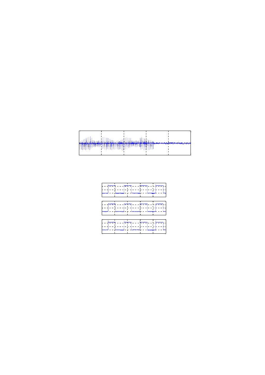
frequency domain give us the false impression, that the EMI signal is periodic. Actually, from the
time-domain measurement, the noise shows periodicity only in a short time interval. In different time
intervals, the amplitude is not fixed. One example is given in Fig. 1, the noise level measured by Line
Impedance Stabilization Network (LISN) presents different levels besides the 50Hz ripple during a
positive half period of the mains frequency. The time-domain approach can provide complementary
information missed by the frequency domain approach.
Authorized licensed use limited to: UNIVERSITEIT TWENTE. Downloaded on October 14, 2008 at 05:31 from IEEE Xplore. Restrictions apply.
In time domain approach, for easier observation and analysis, the drive is set to work under a certain
test mode. We expect these characteristics for the selected test mode:
z
It can be realized by software or signal generator easily.
z
Effects generated by some mechanisms are minimized. That simplifies the analysis. The
remaining effects are maximized for easier observation.
In [1], three coupling path models are identified in time domain for a single-phase diode rectifier half-
bridge converter. For a three-phase diode front-end converter, the EMI propagation is more complex.
In [2], the diode conduction patterns are analyzed. The time-variant frequency spectrum is verified by
zero-span function of a spectrum analyzer. In this paper, the voltage method used to identify the
coupling modes in [1] is replaced by the current probe method [3], and the EMI propagation paths for
the 3-phase converter are identified in the time-domain. The drive system runs in a special test mode,
so that the complexity to analyze the three-phase system is reduced. In this test mode, the gate signals
for different phase poles turn on and turn off synchronously in carrier frequency. The duty ratio is
fixed at 50%. The gate signals for three phase inverter are shown in Fig. 2.
0
2
4
6
8
10
-1
0
1
V
LI
SN
[V
]
Time [ms]
Fig. 1 The EMI voltage of a motor drive measured via LISN, of phase L1
0
100
200
300
400
500
-1
0
1
2
3
duty cycle 50%, u=v=w
V
gu
[V
]
0
100
200
300
400
500
-1
0
1
2
3
V
gv
[V
]
0
100
200
300
400
500
-1
0
1
2
3
V
gw
[V
]
Time [
µs]
Fig. 2 Gate signal used for CM test mode
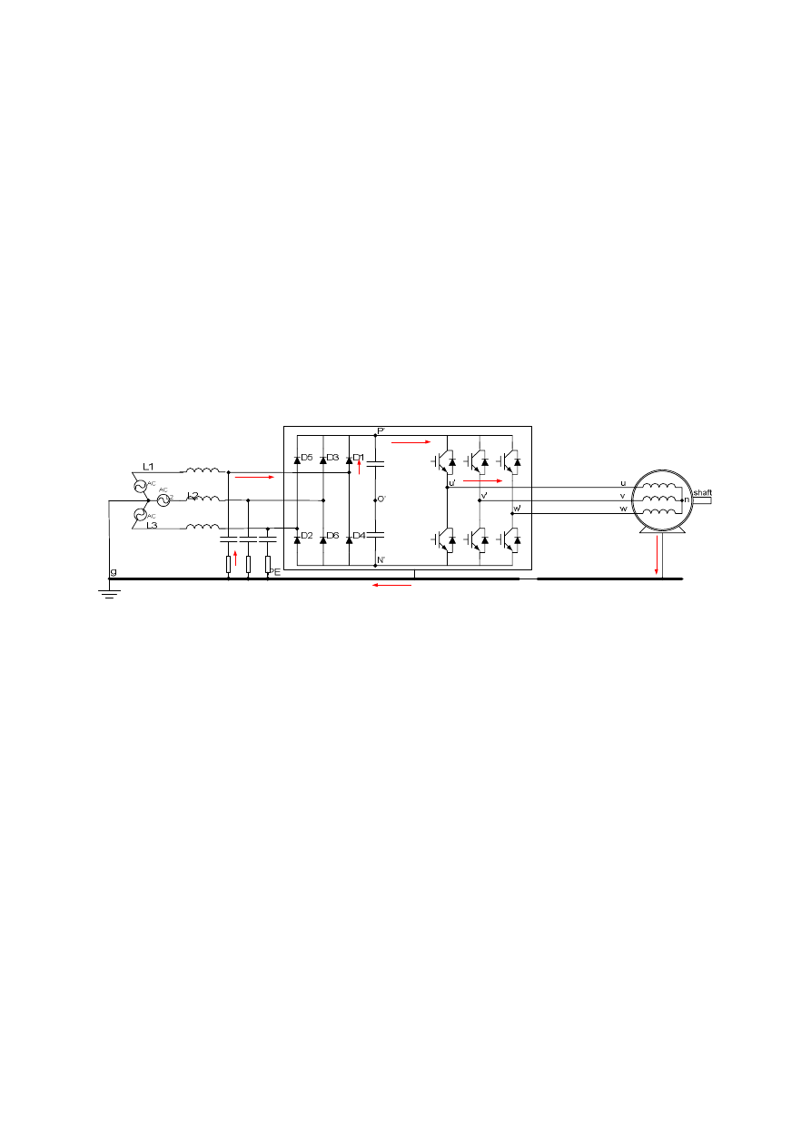
Experimental plant description
In Fig. 3, the experimental plant configuration is illustrated. It is a typical PWM drive system. The
power circuit is an industrial IGBT converter which is produced by Danfoss (VLT5016) with diode
rectifier. It feeds a 7.5kW induction motor operating at 30Hz. The carrier frequency is 8 kHz. An
interface board from Aalborg University replaces the slot for the original control board and translates
the PWM signal into the gate signal for drive circuit with dead-time and protection functions. The
external PWM signal is provided by an EzDSP board produced by Digital Spectrum (eZdspF2808). It
gives flexibility of arbitrary PWM signal generation. Vissim is used for programming and the running
code can be generated and downloaded to eZDSP board. To get galvanic isolation, plastic optic fibers
are used to connect interface card with the PWM DSP board.
Authorized licensed use limited to: UNIVERSITEIT TWENTE. Downloaded on October 14, 2008 at 05:31 from IEEE Xplore. Restrictions apply.
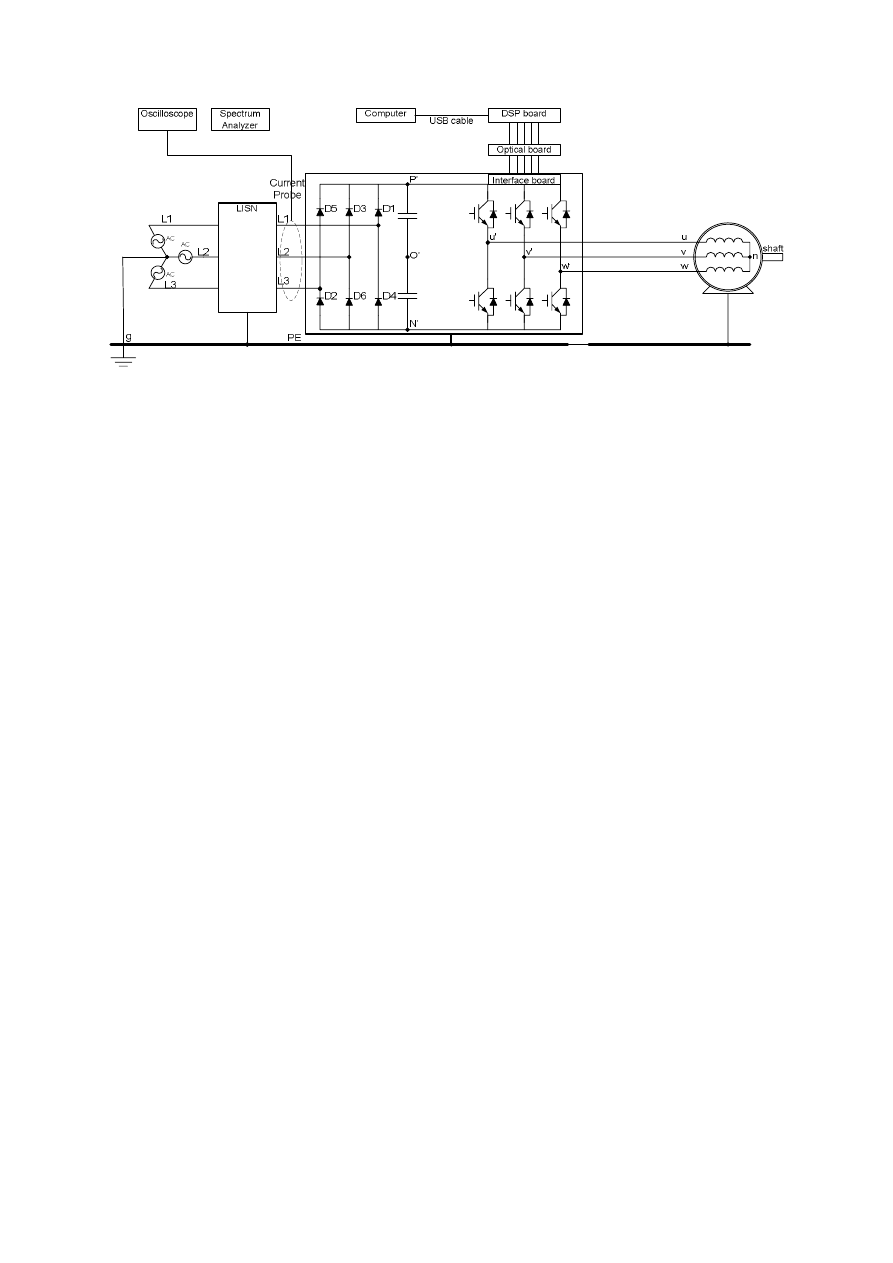
Fig. 3 Functional diagram of test setup
All the CM filtering components and some of the DM filtering components are removed before the
measurement. The remaining DM filtering components including DC capacitor cannot be removed
because of their functionality. The whole drive including motor and LISN are placed on two pieces of
brass plates connected by a brass strip.
Noise source
The switching transient is the main source of CM current. With the output voltage abruptly changing
from low to high, the CM current is flowing from the inverter terminal to the motor cable to charge the
parasitic capacitor between the cable and the reference plate, and the capacitor between the motor
winding and the ground. A positive pulse is expected in this transient. In the fall edge of output
voltage, the negative pulse current is generated by discharging these parasitic capacitors.
In CM test mode, the three poles of the inverter are set to be switched at the same time. Overlaps are
expected which make the amplitude of CM current three times higher. Although slight phase shifting
exists between different switching poles, the DM current generated is much lower than when the
motor runs in normal operation. The DM current is also filtered by the DC capacitors when it is
propagating to the line side. Therefore, the DM current is negligible compared to the CM current in
the line side of the converter in this test mode.
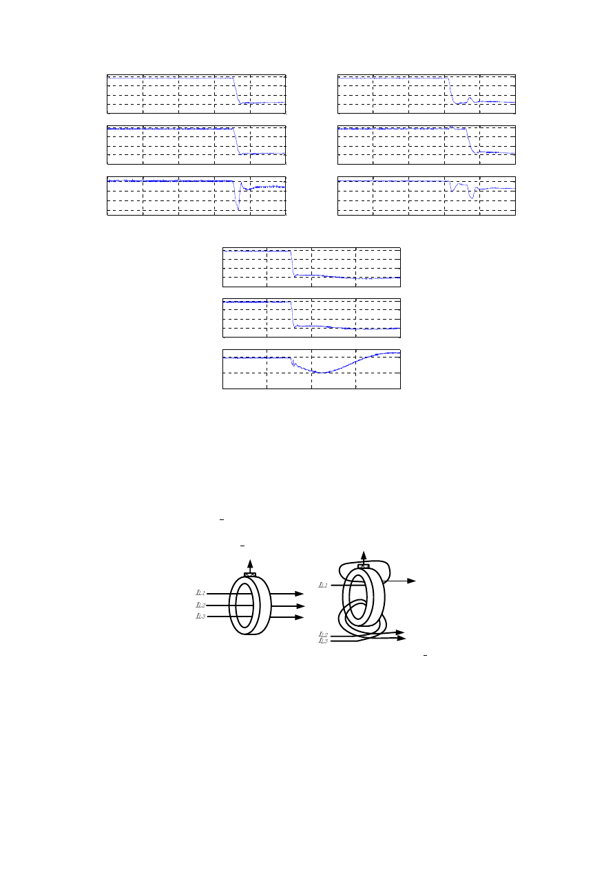
In Fig.4, the measurement shows clearly this causality. The CM current is brought about by the
switching action. When two poles of inverter switch simultaneously, the amplitude of CM current is
doubled as Fig.4 (a) shows. While more frequently, the overlap does not occur, like Fig.4 (b)
illustrates. A higher resonant frequency of 2.2MHz can be recognized in this figure. Another lower
resonant frequency also appears around 60 kHz which is shown in Fig. 4(c).
Actually, due to the limitation of DSP’s calculating speed and the gate drive delay-induced error [4],
the transition of the phase voltages have a variable delay time between each other. A typical delay
between phases is varying in a range of 260ns. Therefore, the overlap occurs all the time for the
resonance of 60 kHz because the period of the resonance is much longer than the deviation of delay.
For the resonant signal of 2.2MHz, the overlap occurs occasionally but not all the time.
Authorized licensed use limited to: UNIVERSITEIT TWENTE. Downloaded on October 14, 2008 at 05:31 from IEEE Xplore. Restrictions apply.
0
2
4
6
8
10
-200
0
200
400
600
V
u'
N'
[V]
0
2
4
6
8
10
-200
0
200
400
600
V
v'
N
'
[V
]
0
2
4
6
8
10
-6
-4
-2
0
I
CM
2
[A]
Time [
µ
s]
0
2
4
6
8
10
-200
0
200
400
600
V
u'
N'
[V]
0
2
4
6
8
10
-200
0
200
400
600
V
v'
N
'
[V
]
0
2
4
6
8
10
-6
-4
-2
0
I
CM
2
[A]
Time [
µ
s]
(a) (b)
0
5
10
15
20
-200
0
200
400
600
V
u'
N'
[V]
0
5
10
15
20
-200
0
200
400
600
V
v'
N
'
[V
]
0
5
10
15
20
-4
-2
0
I
CM
2
[A]
Time [
µ
s]
(c)
Fig. 4 Measurement of CM current in the inverter motor side
Propagation path identification
The CM current is generated in the inverter output side and propagated to the line side. We use two
current probes to measure the current in the line side of the converter. Using the different wiring
configurations depicted in Fig. 5, we get two measurement results. I
CM1
is the common mode current in
the line side of the inverter. I
DM1_L1
is the differential mode current in the line side of the inverter. As
said previously, the DM current is ignorable when the converter operates in common mode test mode.
Therefore, the measured current I
DM1_L1
is actually the MM current.
(a) I
L1
+ I
L2
+ I
L3
= 3I
CM1
(b) 2I
L1
- I
L2
- I
L3
= 3I
DM1_L1
Fig. 5 Using current probe to separate CM and DM
The test result is presented in Fig. 6 (a). To get more details, we zoom in for the different scenarios, as
shown in Fig. 6 (b)-(d).
By observing these figures, the features are summarized below for different scenarios.
Authorized licensed use limited to: UNIVERSITEIT TWENTE. Downloaded on October 14, 2008 at 05:31 from IEEE Xplore. Restrictions apply.
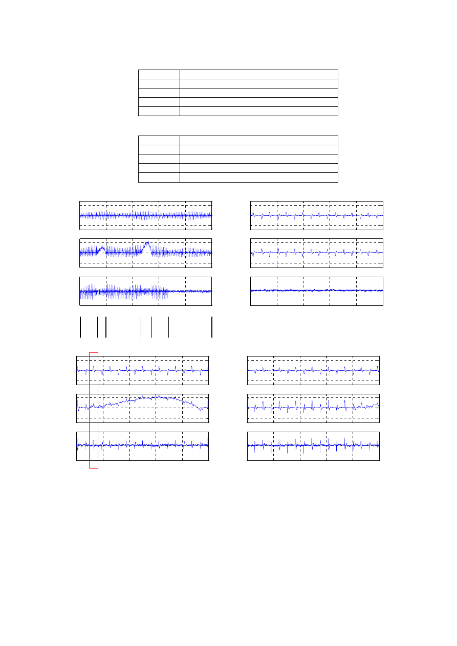
Table I: The relation between I
CM1
and I
DM_L1
in different scenarios
Scenario Relation
between
I
CM1
and I
DM_L1
#1
I
DM_L1
= - I
CM1
#2
I
DM_L1
= ½ I
CM1
#3
I
DM_L1
= 2 I
CM1
and I
DM_L1
= - I
CM1
by turns
#4
I
DM_L1
= 0.8 I
CM1
Table II: The relation between I
CM1
and V
LISN
in different scenarios
Scenario Relation
between
I
CM1
and V
LISN
#1
V
LISN
= 0
#2
V
LISN
= 25 I
CM1
#3
V
LISN
= 50 I
CM1
and V
LISN
= 0 by turns
#4
V
LISN
= 30 I
CM1
0
2
4
6
8
10
-5
0
5
I
CM
1
[A]
0
2
4
6
8
10
-5
0
5
I
DM
1
L
1
[A
]
0
2
4
6
8
10
-1
0
1
V
LI
SN
[V]
Time [ms]
0
0.2
0.4
0.6
0.8
1
-5
0
5
I
CM
1
[A]
0
0.2
0.4
0.6
0.8
1
-5
0
5
I
DM
1
L
1
[A
]
0
0.2
0.4
0.6
0.8
1
-1
0
1
V
LI
SN
[V]
Time [ms]
0
0.2
0.4
0.6
0.8
1
-5
0
5
I
CM
1
[A]
0
0.2
0.4
0.6
0.8
1
-5
0
5
I
DM
1
L
1
[A
]
0
0.2
0.4
0.6
0.8
1
-1
0
1
V
LI
SN
[V]
Time [ms]
0
0.2
0.4
0.6
0.8
1
-5
0
5
I
CM
1
[A]
0
0.2
0.4
0.6
0.8
1
-5
0
5
I
DM
1
L
1
[A
]
0
0.2
0.4
0.6
0.8
1
-1
0
1
V
LI
SN
[V]
Time [ms]
Fig. 6 Conducted emission measurement result in the line side of converter
Via the observation of the relationships between the waveforms, as tabulated in Table I and Table II,
we know directly how the diode conduction patterns correspondent to the scenarios we measured.
Scenario 1 happens when diode pair D2/D3 or diode pair D5/D6 pair are conducted. The CM current
would not flow through D1 or D4, the LISN in phase L1 would not detect the noise.
scenario 4
3 2
2 3
1
3
scenario
(b) Zoom in of scenario 1
(a) measured waveform and scenarios
(c) Zoom in of scenario 2
(d) Zoom in of scenario 3
Authorized licensed use limited to: UNIVERSITEIT TWENTE. Downloaded on October 14, 2008 at 05:31 from IEEE Xplore. Restrictions apply.
Scenario 2 is also a very familiar situation, when the diode pair D1/D2, or D3/D4, or D4/D5, or D6/D1
are conducted. The CM current ripple is superimposed on the rectifier input DM current.
Scenario 3 is recently introduced by [1], [2], and [5]. At the moment when the gate signal turns on the
upper switch or turns off the lower switch, the inverter terminal U’ is still in low voltage potential
because of the parasitic capacitor. The D1 is conducted by this positive bias voltage. D2 or D6 are
reverse biased because the voltage in DC bus capacitor clamps the potential of their anodes lower than
the potential of their cathodes. Therefore, the current flows only through L1. The loop of the CM
current is illustrated in Fig. 7 below. A similar situation happens when the gate signal turns off the
upper switch or turns on the lower switch, the inverter terminal U’ is equal to the potential of positive
DC bus. That makes all the current flowing through L2 or L3, while keeps the D1 reverse biased. One
notes that the MM mode will disappear when X capacitors are installed. That causes the current to be
located evenly between the phase lines. Because the value of X capacitor is limited, there is always
more or less unbalance. Therefore, MM needs to be considered especially in low frequency.
The scenario 4 is observed in the transit time between the scenario 2 and the scenario 3. It is marked in
Fig.6 (c). This scenario happens when the only conducted diode is handing over part of the CM
current to another diode which is becoming conducted.
Fig. 7 The loop of CM current of scenario 3
In the measured waveforms, we also found that the CM noise presents a replicated ripple shown in
Fig.6 (a). The period of the ripple is right the interval of 1/6 mains voltage period. That confirms that
the CM current is generated by voltage transient and is proportional to this transient voltage change
ratio.
Upper boundary for EMI
The common mode test mode is used in the last section to identify the noise propagation path
successfully. Because the DM noise is minimized, the complexity of the analysis is reduced. Here,
another interesting usage of common mode test mode is finding the upper boundary of common mode
noise when converter operates normally. That is because that the CM noise is maximized in CM test
mode. As we indicated in Fig. 4, in the CM test mode, the three inverter leg switching is synchronized.
The overlap is expected for the frequency range below 150 kHz. In this frequency range, the delay
error of switches is far short than the noise period.
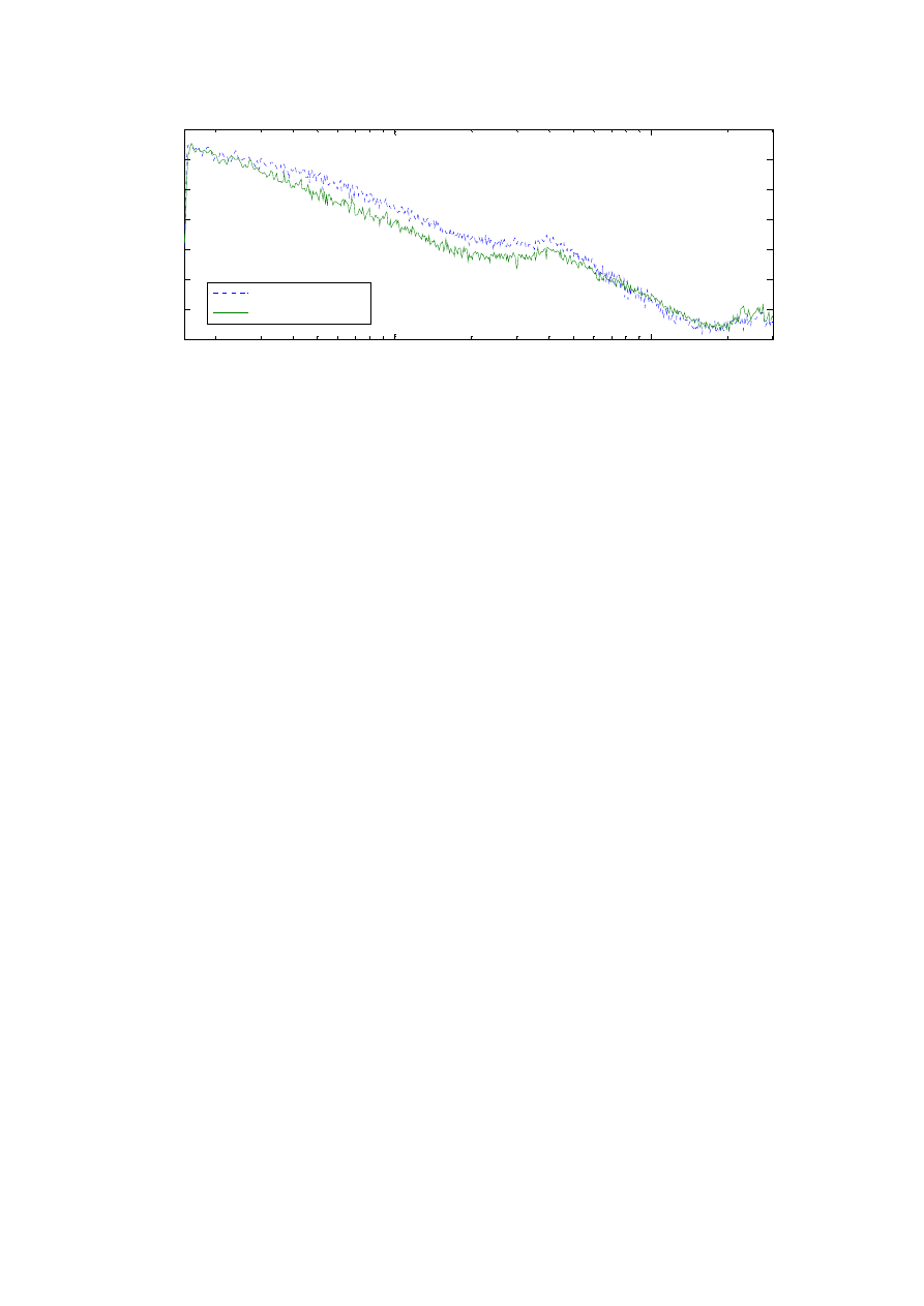
Notice from the measurement result shown in Fig. 8 (a), in the frequency range between 30 kHz till
150 kHz, the level difference between CM test mode and normal operation is around 9dB. That is as
expected: 20*log
10
3=9.5dB, because the total level is tripled compare to normal operation.
For the frequency range between 1MHz-10MHz, the noise is determined by the on/off transitions of
switches. In CM test mode, because no functional current is established, the load current is quite low.
Therefore, the dv/dt of the transistor turn off is very small. The duration of turn off transit is even
longer than the deadtime. That makes that the terminal voltage is driven to the bus voltage rapidly by
the complementary IGBT turning on each time the dead time has expired. The waveform of this turn
Authorized licensed use limited to: UNIVERSITEIT TWENTE. Downloaded on October 14, 2008 at 05:31 from IEEE Xplore. Restrictions apply.
off is given in Fig.9. Therefore, in CM test mode, the dv/dt of noise source has fast slopes in both
transients of turn-on and turn-off. Compare with normal operation mode, the dv/dt is high in turn on
and low in turn off, the EMI level of the CM test mode is 20*log
10
2= 6dB higher, that is consistent
with the measurement result given in Fig.10.
10k
100k
150k
60
80
100
120
Frequecncy (Hz)
N
o
is
e
L
e
v
e
l (
d
B
µ
V)
CM Test Mode
Operation Mode
Fig. 8 The EMI measured by LISN when motor in normal operation and CM test mode (9kHz-
150kHz)
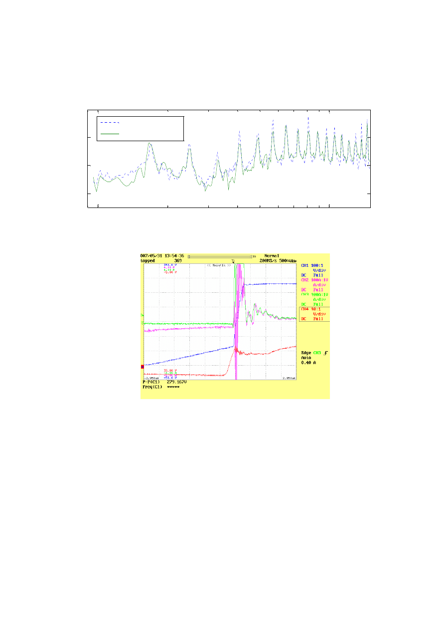
Fig. 9 The IGBT turning off follows by turn on of complementary IGBT in CM test mode (500ns/div)
CH1: voltage between output terminal and negative DC bus (100V/div) CH2: phase currentv
(0.5A/div) CH3: current of upper switch (IGBT+diode) (0.5A/div) CH4: gate signal of upper IGBT
(5V/div)
100
10
0.5
0.5
CH3
CH2
CH1
CH4
Authorized licensed use limited to: UNIVERSITEIT TWENTE. Downloaded on October 14, 2008 at 05:31 from IEEE Xplore. Restrictions apply.
1M
10M
30M
50
60
70
80
90
100
110
120
Frequecncy (Hz)
N
o
is
e Le
v
e
l (
d
B
µ
V)
CM Test Mode
Operation Mode
Fig. 10 The EMI measured by LISN when motor in normal operation and CM test mode (150kHz-
30MHz)
Conclusion
In this paper, the CM test mode is defined and used to identify the noise propagation path. There are
three reasons for our interest in the CM test mode.
1. It is easy to implement, and can be applied in site after the installation.
2. The DM noise is minimized, that makes the analysis and measurement simpler.
3. The CM and MM noise is maximized. That gives the “worst situation” and upper boundary of
the EMI noise when the test unit is in normal operation.
A suggestion is adding the CM test mode in the software and using it to choose correct suppression
components.
References
[1] J. Meng, W. Ma, L. Zhang, and Z. Zhao, “Identification of essential coupling path models for conducted EMI
prediction in switching power converters,” in Proc. IEEE Industry Applications Soc. Conf. (IAS), vol. 3, 2004,
pp. 1832-1839.
[2] W. Shen, F. Wang, and D. Boroyevich, “Conducted EMI characteristic and its implications to filter design in
3-phase diode front-end converters,” in Proc. IEEE Industry Applications Soc. Conf. (IAS), vol. 3, 2004, pp.
1840-1846.
[3] G. Grandi, D. Casadei, and U. Reggiani, “Common- and differential-mode HF current components in AC
motors supplied by voltage source iInverters,” IEEE Trans. Power Electronics, vol. 19, no. 1, pp. 16–24, Jan.
2004
[4] R. J. Kerkman, D. Leggate, D. W. Schlegel, and C. Winterhalter, “Effects of parasitics on the control of
voltage source inverters,” IEEE Trans. Power Electronics, vol. 18, no. 1, pp. 140-150, Jan. 2003.
[5] S. Qu and D. Chen, “Mixed-mode noise and its implications for filter design in offline switching power
supplies,” IEEE Trans. Power Electronics, vol. 17, no. 4, pp. 502-507, July 2002.
Authorized licensed use limited to: UNIVERSITEIT TWENTE. Downloaded on October 14, 2008 at 05:31 from IEEE Xplore. Restrictions apply.
Wyszukiwarka
Podobne podstrony:
[2001] State of the Art of Variable Speed Wind turbines
[2001] State of the Art of Variable Speed Wind turbines
[2001] State of the Art of Variable Speed Wind turbines
0401 safety chain solution safe stop1 variable speed drive
Lqg Multiple Model Control Of A Variable Speed Pitch Regulated Wind Turbine
Control Issues Of A Permanent Magnet Generator Variable Speed Wind Turbine
Grid Impact Of A 20 Kw Variable Speed Wind Turbine
Variable Speed Control Of Wind Turbines Using Nonlinear And Adaptive Algorithms
historical identity of translation
Identification of Dandelion Taraxacum officinale Leaves Components
Innovative Solutions In Power Electronics For Variable Speed Wind Turbines
Dental DNA fingerprinting in identification of human remains
20050253396 Variable Speed Wind Turbine Generator
Analysis of spatial shear wall structures of variable cross section
historical identity of translation
The identity of the Word according to John [revised 2007]
Computer Virus Propagation Model Based on Variable Propagation Rate
więcej podobnych podstron