
1 2
A C++ Programming Tutorial
by Mike Podanoffsky
2 2
Characterizing Processor Performance
by Rick Naro
2 6
Designing with
by Rick Lehrbaum
3 6
An LCD and Keypad Module for the SPI
by Brian
OUR BONUS
HOME AUTOMATION BUILDING
SECTION BEGINS ON PAGE 47 OF THIS ISSUE!
8 2
q
9 2
q
9 8
q
1 0 6
q
Firmware Furnace
Journey to the Protected Land: With Interrupts, Timing is Everything
Ed Nisley
From the Bench
Vaporwear: Revealing Your Humidity
Bachiochi
Silicon Update
A Saab Story
A Tale of Speed and Acceleration
Tom
Embedded Techniques
Using Keyboard I/O as an Embedded Interface
Dybowski
Editor’s INK
Ken Davidson
A Reaffirmation
New Product News
edited by Harv Weiner
Excerpts from
the Circuit Cellar BBS
conducted by
Ken Davidson
Steve’s Own INK
Steve Ciarcia
One of Those Days
Advertiser’s Index
Circuit Cellar INK
Issue
April 1995
3
Edited by Harv Weiner
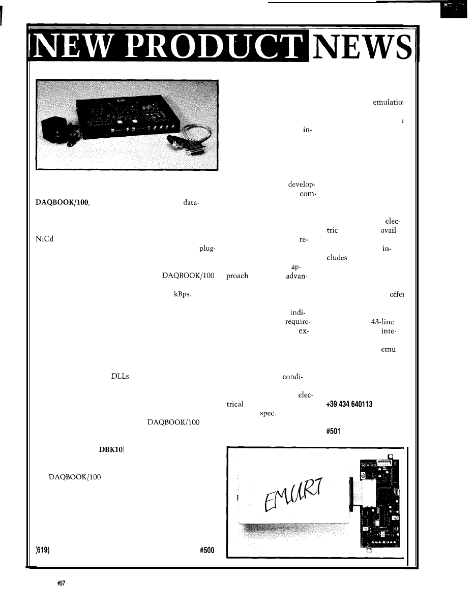
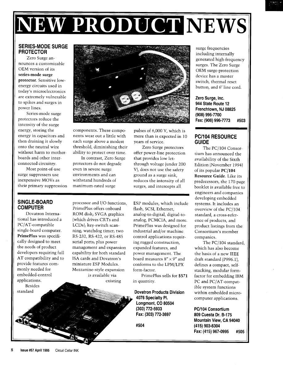
SERIAL EPROM EMULATOR
Softec Microsystems
[the basic version in-
introduces a serial EPROM
cludes a l-Mb
emulator that doesn’t re-
RAM). In addition to
quire removal of the system
loading the object code
microprocessor. Unlike
the rate of 115,200 bps,
circuit emulators that re-
receives the traditional
place the microprocessor
binary, Motorola-S, and
with a pod, the EMUR7
Intel hex formats. The
replaces and emulates the
EMUR7 connects to a
PORTABLE DATA ACQUISITION SYSTEM
system EPROM. Designers
PC-compatible compute
then use their own
through the serial port
Industrial Computer Source has announced
ment tools [assembler,
and does not need a
a high-speed, multifunction,
piler, and linker) to execute
power supply. The unit
acquisition subsystem for notebook PCs. Power to the
object code on the test board
can be connected to a
unit may be supplied by a number of sources: a 12-V car
as if a new EPROM had
portable PC when
battery, 120-VAC line power, or an optional rechargeable
been programmed. This
power is not
battery.
eliminates the need to
able.
The unit combines the functionality of several
move, erase, reprogram, and
The EMUR7
in analog and digital data-acquisition boards in an
reinsert the EPROM.
a friendly user
external module the size of a notebook PC. Attaching
This emulation
interface with working
directly to a portable PC’s parallel port,
has several
selections and options
provides 16 single-ended or 8 differential inputs with a
tages. The emulator is truly
clearly and efficiently
bidirectional data-transfer rate of up to 170
universal and the designer
displayed. The unit
Acquired data can be stored real time in the PC’s
may choose the family or
full mouse support, a
memory and hard drive.
processor satisfying
context-sensitive help
Software includes full-featured DOS and Windows
vidual application
feature, and a
drivers for C, BASIC, and Visual Basic. As well,
ments without buying
video mode. The
DaqView, a Windows graphics application, enables the
pensive in-circuit emulators
grated ROM editor lets
user to set up an application to acquire and save data
for different processors.
users modify the
directly to disk or to seamlessly transmit it to other
Another advantage is that
lated code.
Window applications. VISUALAB is another software
the test circuit works under
option, offering a set of
to extend the capabilities
normal operating
Softec Microsystems
of Visual Basic and Snap-Master for Windows. This
tions-the real microproces-
33082 Azzano Decimo (PN
advanced software package integrates data acquisition,
sor guarantees that all
Italy
high-speed data streaming to disk, data retrieval, and
and time parameters
analysis.
comply to
Fax: t39 434 631598
In addition to portable testing,
is
EMUR7 supports
ideal for remote data-collection applications such as
EPROM devices up to 8 Mb
automotive and aviation in-vehicle testing. An expan-
sion chassis (Model
provides connection for
multiplexers, thermocouple cards, a strain-gauge
interface, and more digital channels.
sells for $1295 and includes an AC
adapter, parallel-port cable, DOS and Windows drivers,
and DaqView software. The expansion chassis sells for
$150.
Industrial Computer Source
3950 Barnes Canyon Rd.
San Diego, CA 92121
677-0877
l
Fax: (619) 677-0898
6
Issue
April 1995
Circuit Cellar INK
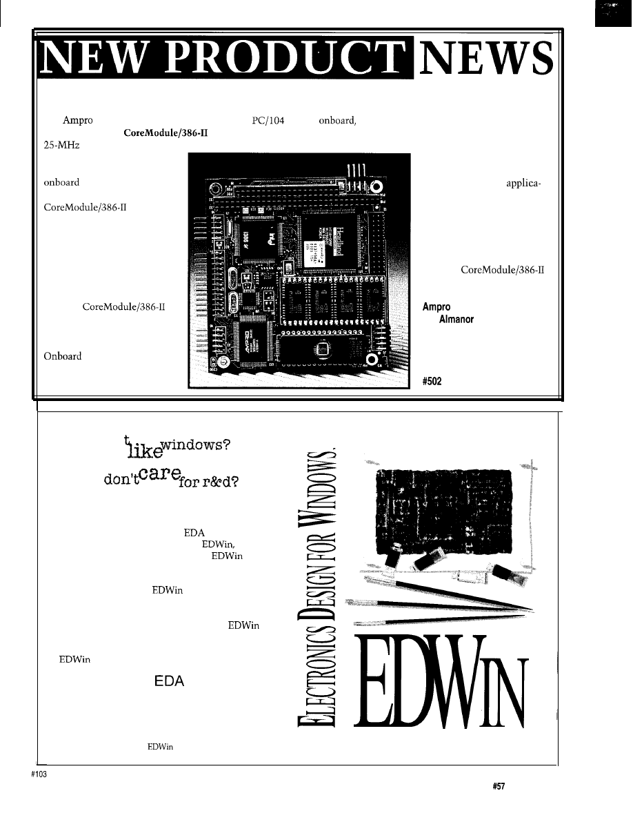
‘386SX MODULE
port, as well as standard keyboard and speaker interfaces.
Computers is offering a new ‘386SX
An
bootable solid-state disk assures reliable
CPU module. The
is based on Intel’s
operation in harsh operating environments. Watchdog
‘386SX CPU and
timer and power monitor
includes two serial ports, up
functions are also included
to 16 MB of DRAM as well as
to ensure maximum system
NVRAM or a flash
integrity in critical
memory, solid-state disk.
tions. The module operates
complies
with approximately 3 W
with the newly adopted PC/
(active mode) of power and is
104 (V. 2) standard. Typical
designed for use in extended
applications include medical
temperature environments of
instruments, vehicular data
o-70°C.
acquisition and control
The
systems, and portable test
sells for $359 in quantity.
equipment.
The
Computers, Inc.
contains the equivalent of a
990
Ave.
complete PC/AT motherboard
Sunnyvale, CA 94086
and several expansion cards.
(408) 522-2100
I/O functions
Fax: (408) 720-l 305
include two RS-232 serial
ports, a bidirectional parallel
don’
sorry.
Then we just can’t help you. But if you’re looking for
a high-capacity, user-friendly
system, we’ve got
just what you need. Say “hi” to
your new
companion in Electronics Design.
features
seamless integration between modules, so you can
finally kiss the tedious concept of front- and back
annotation goodbye.
gives you all the tools
you’ll need, and is so user-friendly you can even
compile your own custom toolboxes. So easy to learn,
you’ll be up and running in minutes,
also
features nice pricing, starting at just $495.
Make your appointment with us today for the
evaluation package. Welcome.
Vision
Corp.
995 E
Baseline
Rd. Ste 2166,
Tempe, Arizona 85283-l 336
Phone: I-800-EDA-4-YOU, or (602) 730 8900
Fax: (602) 730 8927
is a trademark of Norlinvest Ltd. Windows is a trademark of Microsoft
Corp.
Circuit Cellar INK
Issue
April 1995
7
ANSI-FORTH
up to 512 KB of
for data logging, robotics, or
DATALOGGER AND
in solving control
backed RAM, EEPROM, or
machine control. Up to 33 I/
problems. A PC library of
CONTROLLER
flash memory. In addition, a
0 lines, two RS-232 serial
ANSI-Forth software
Saelig Company
miniature hard drive
lines, an
bus, real-time
makes stepper-motor
introduces a tailor-made
is available and 32 digital
clock, and watchdog timer
control, interrupt
data-collection system
inputs may be monitored.
make an economical,
handling, real-time
that can be read by a PC
An
S-channel,
versatile controller for a
multitasking, data
and features removable
A/D converter and
wide range of applications.
logging, serial I/O,
card memory. The
channel,
D/A
Although small, it is packed
keyboard, and LCD
TDS2020 Data Logger
verter make the 4” x 3”
with important features
driving easy. When
Module adheres to the
board extremely versatile
which make it easy to use
logging data in standby
official Forth language
mode, it will run on 500
definition. Forth is an
so a 9-V battery lasts
easily-learned, high-level
language ideal for fast
The TDS2020 sells
control and well-suited
for $499 for the starter
to real-time embedded
pack, which includes a
systems.
comprehensive manual
The TDS2020 is a
and PC software.
control computer
The Saelig Company
532 CMOS microproces-
sor running at 20 MHz. It
is available with 16 KB of
ANSI-Forth kernel, a full
Fax: (716) 425-3835
symbolic assembler, 45
KB of program space, and
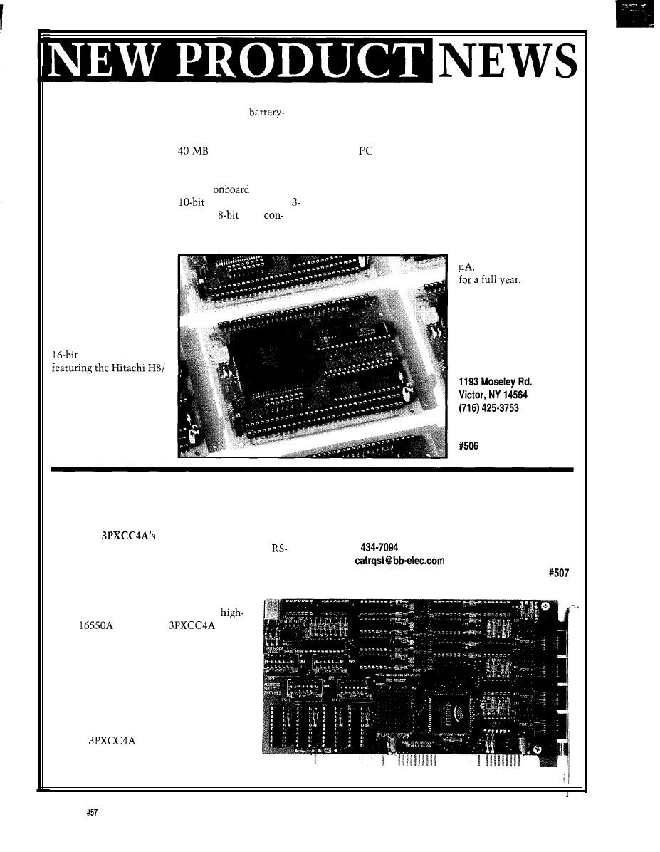
FOUR-PORT SERIAL BOARD
B&B Electronics Manufacturing Co.
A PC-compatible serial card, featuring four serial
P.O. Box 1040
ports in a single slot, is available from B&B Electronics.
Ottawa, IL 61350
Each of the
ports can be independently
(815) 434-0846
configured for any I/O address and IRQ as well as
Fax: (815)
232, RS-422, or RS-485 data protocols, allowing it to fit
Internet:
any serial application.
TD, RD, RTS, CTS, DSR, DCD, and
DTR port lines are supported by the RS-232
mode with each port using a buffered,
speed
UART. The
has
interrupt-sharing capabilities and an
interrupt status register to increase through-
put in shared IRQ applications and the
number of available interrupts in a system.
The card features eight-conductor RJ-45
connectors. Prewired adapter kits (Models
MDB9 and MDB25) are available to convert
the RJ-45 to DE9 or DB25 connectors.
The
sells for $209.95 and the
cable adapters are $10.95 each.
10
Issue
April 1995
Circuit Cellar INK
FEATURES
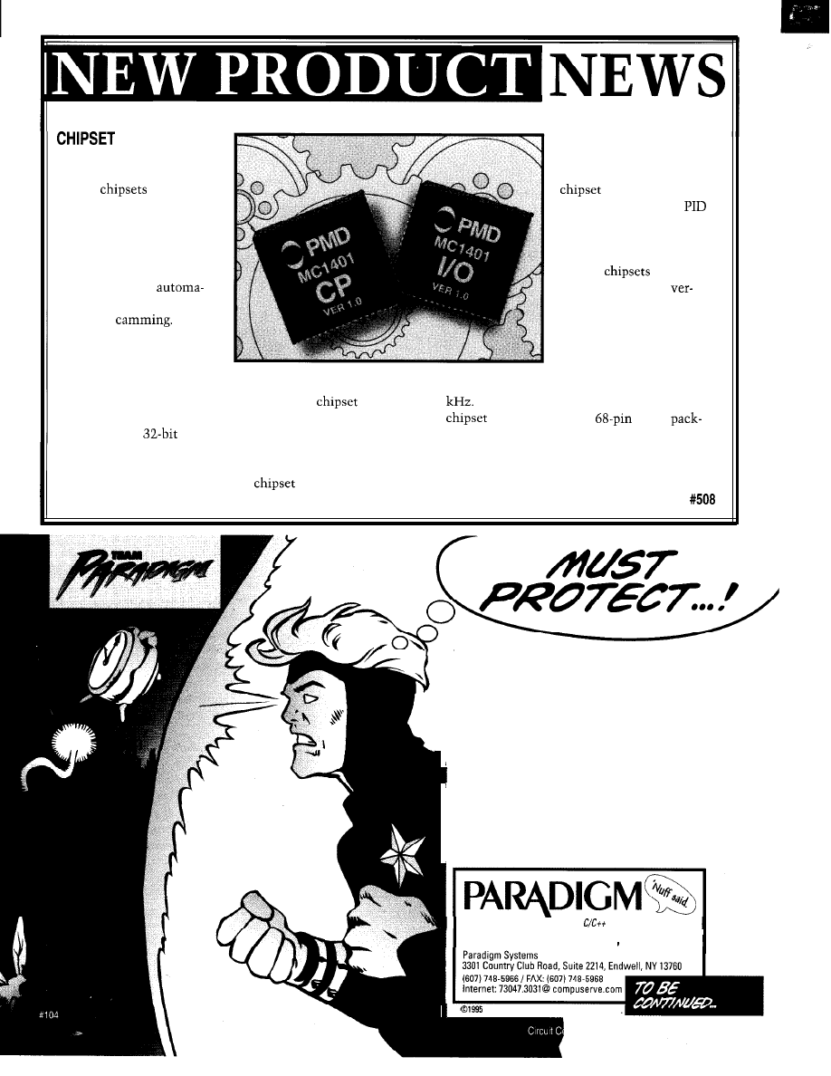
ELECTRONIC GEARING
velocity contouring) along
with high-resolution, 16-bit
The MC1401 family of
DAC output signals. The
motion
from PMD
provides closed-loop
now supports up to two axes
control using either a
of servo-based electronic
loop or a PI with velocity
gearing. Electronic gearing
feed-forward feedback loop.
can be used in numerous
The MC 140 1 -series of
applications including
motion
are
robotics, medical
available in several
tion, coil winding, and
sions, including one that
electronic
supports incremental
The required elements
encoder input. Another
for electronic gearing are a
supports absolute digital
master input-axis encoder
and resolver-based input
and a servo-controlled slave axis. The position of the
and a third version supports sinusoidal commutation at
master axis is continuously monitored by the
up to 15
and is used to drive the slave axis after going through a
The
is made up of two
PLCC
programmable
gear ratio. A special feature is that
ages and sells for $99 in quantity.
the master axis can itself be servo controlled, allowing
the user to create tightly coupled multiaxis systems.
Performance Motion Devices, Inc.
Other standard features of the
include three
11 Carriage Dr.
l
Chelmsford, MA 01824
user-selectable profiling modes (S-curve, trapezoidal, and
(508) 256-l 913
l
Fax: (508) 256-0206
Proven Solutions for Embedded
Developers
Development tools alone aren’t sufficient to
make your ‘186 or V-Series design a success. Here
at Paradigm, we have the tools, experience and
commitment to see your design through to
completion.
Start with Paradigm LOCATE and Paradigm DEBUG.
1
If, along the way, you stumble or hit a brick wall,
call Team Paradigm for help:
I
l
Toll-free technical support
l
24-hour BBS support
l
Paradigms customer newsletter
After all, life is tough enough without worrying
about your development tools. Choose Paradigm
and enjoy sleeping again at night.
I-800-537-5043
I
Paradigm Systems, Inc. All rights reserved

FEATURES
Programming Tutorial
Mike Podanoffsky
Characterizing
Processor Performance
Designing with
04
An LCD and Keypad
Module for the SPI
A Ctt
Tutorial
0
his article
should probably
be entitled “C++ For
Those Who Already
Know C,” but I’ll try to be general
enough for everyone. C++ was born at
AT&T in the 1980s. It was a set of
object-oriented extensions to C, an
already popular language. The change
from C’s largely procedural view to
object view marks a fundamen-
tal paradigm shift-one that changes
how all programs and all programming
problems are viewed.
Listing 1 demonstrates this
sweeping claim. As you can see, this is
a simple and perfectly correct portion
of a C program. But, what is wrong
with it?
The code is typical of C which
publishes
DATA L I
as a public struc-
ture. The logic that manipulates its
members is sprinkled throughout
many different application programs.
DATA L I
structure was changed,
every program using it would need to
be altered or at least recompiled. With
this procedural framework, knowledge
is said to be
distributed.
With C++, programs do not know
or have direct access to members of a
data structure. Instead, they call a
function, specifically known as a
member function
or
method,
to
retrieve members of the data structure.
12
Issue
April 1995
Circuit Cellar INK
Listing 1-A typical C program relies on distributed know/edge about data structures.
DATALIB
while
Received at: %d:%d %d
DataLib.Hour,
? "RISING" "FALLING");
Although this represents cost in the
number of instructions generated to
achieve data-structure independence,
it limits the dependencies to a few
well-defined interfaces. The interfaces
provide access functions to some of
the data in the private section.
It isn’t generally true that perfor-
mance degrades overall by the object
model. In some cases, the model
allows for code generation that
increases a program’s performance. I’ll
sprinkle advice about the type of code
C++ generates throughout this article.
Note: Data independence is not
limited to
The same effect can be
created using C or assembly language.
A text file, en
c
a p s c
(available on
the Circuit Cellar BBS), describes how
to achieve the same effect in C.
Although I’ll talk about how the
switch to C++ represents a shift in
thinking, I cannot provide a thorough,
profound, and well-developed tutorial
of a language as complex as C++
within the confines of a single article.
At best, I can provide sufficient
examples of the salient points of
I’ll begin with a practical example
emulating an answering machine’s
behavior. Because it is a system with
controls, inputs, and outputs, it offers
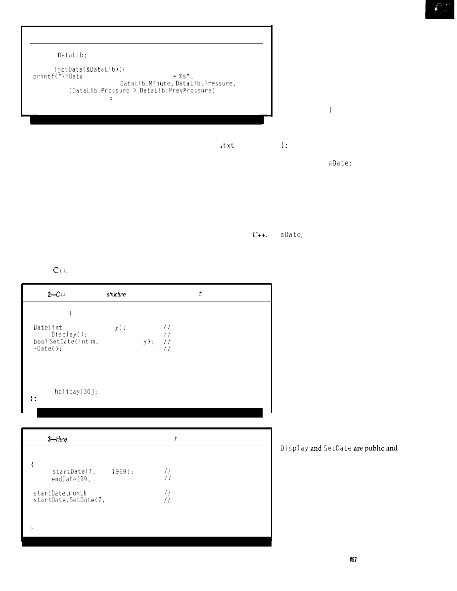
Listing
encapsulates data
and behavior as shown in fhis Da e class.
class Date
public:
m, int d, int
constructor
void
display function
int d, int
set date
destructor
private:
int
month;
int
day:
int
year:
char
Listing
are examples of how (and how not) to use the Da e class.
void main0
Date
20,
declare a Date
Date
999, 9999):
an invalid Date
= 6:
this is illegal
20, 1994);
set a date
startDate.DisplayO;
endDate.DisplayO;
similar types of problems to those
found in most embedded applications.
However, let’s start with the
basics.
AN INTRODUCTION TO CLASSES
In C, a data structure would be
defined and used as:
struct Date
int
month;
int
day;
int
year;
struct Date
aDate.month = 7;
aDate.day = 20;
aDate.year = 1969;
Just to review some basic C, memory
is allocated for a structure called
which is of type Date.
In C++, a programmer declares a
class, which has a similar appearance
(and to some extent, a similar func-
tion) to a data structure. A class
declares both data and the functions
that can access this class. These
function members are known techni-
cally as
methods.
Listing 2 shows how
a class is defined. Note that comments
in C++ begin with two slashes and end
with a carriage return.
The class definition shown in
Listing 2 contains
public
and
private
sections. Anything listed publicly is
accessible from anywhere or any
program. The functions and variables
from a private section can only be
accessed from functions defined in the
Date class.
In this example, the variables
month, day, and year are private and
can only be accessed by the functions
declared in Da t e class. The functions
may be called from anywhere. They
control access to objects in the class.
The functions Da t e and -Da t e are
known as
constructors
and
destruc-
tors,
respectively. They are called
automatically when an instance of the
class is created or destroyed. These
functions serve an invaluable purpose.
Because of the constructors, data in a
class can be initialized when created
Circuit Cellar INK
Issue April 1995
13
and allocated resources can be freed
when destroyed.
Listing demonstrates how a
program uses a class. Two
Da t. e
objects are instantiated (created):
and
Each
declaration causes the constructor, the
Da t. e function, for this class to be
called. The constructor initializes the
object. Unlike other functions,
constructors and destructors cannot
fail and cannot readily report errors
even if the parameters passed are
wrong!
have no way of
returning errors. Because of this, it is
imperative that constructors always
initialize an object to a safe state, even
when illegal parameters are passed.
Thestatement
is illegal because month is a private
member of the
Date
class and cannot
be directly accessed. One solution is to
add a Set
M
O
n t h
method. As defined so
far, a date can be set or displayed by
using its public functions Set
Da t e
and
Display.
CONSTRUCTORS AND
DESTRUCTORS
Instantly, a C programmer can
recognize the value constructors and
destructors provide. With them, an
object always has the opportunity to
properly initialize prior to its use.
This, as with other C++ features, is far
more important when an object is
complex, containing linked lists and
substructures. Constructors and
destructors are part of the object model
and are enforced by the language itself.
A typical constructor appears in
Listing 4. The syntax
Da e
Da e
identifies this as a function belonging
to the
Date
class. The class name
appears to the left and is separated
from the function or method name by
double colons. Constructors always
have the same name as the class to
which they belong.
There can be, in fact, several
constructors defined, each supporting
different arguments types. This is a
feature of C++ functions and methods
and is not limited to just constructors.
C++ matches function calls based on
the argument list and not just on the
function name. This way different
member functions can be defined with
14
Circuit Cellar
INK
Listing
but cannot explicitly return errors
Constructor
m, int d, int
if 1 m
if date is illegal
m = -1:
indicate by a -1 in month
month = m;
day = d;
year = y;
the same name, but have different
for any argument. When the argument
arguments. Listing 5 offers an example
is missing from a call, the default
of this capability.
value is automatically inserted.
It is also possible to avoid having
In Listing 6, the string argument
to declare functions for every
in the
Da e
constructor is defined to
tion of calling parameters because C++
take on a default value of null. If the
supports default parameter values as
string argument is not passed during a
part of the calling convention. A
call, a null value (the default value
default parameter value can be defined
declared in the constructor’s
Listing 5-A class may have many
depending on the arguments passed
class Date
public:
m, int d, int
m, int d, int const char
private:
int
month;
int
day:
int
year:
char
constructor with no arguments
Date::DateO
month = day = 1;
year = 1994:
constructor with mmlddlyy arguments
int d, int
month = m;
day = d;
year = y;
constructor with holiday text argument
m, int d, int y, const char
d,
void main0
Date
Date
20, 1994);
Date
1, 1994, "New Year's Day");
tion) is supplied during the call.
Default parameters are not limited to
constructors.
Finally, you almost always need to
create this next special case of a
constructor for all of your objects. It
would be highly desirable to create a
new object by passing it a reference to
an already existing object. For ex-
ample, it is desirable to be able to
initialize a date object with the value
of another date object.
This type of constructor is called a
copy constructor
because the result is
that the new object becomes a copy of
the referenced object [see Listing 7).
Constructors are optional. If no
constructor is defined, a dummy
constructor is automatically created by
the compiler. The dummy constructor
is called but does nothing, not even
initialize the data structure’s contents.
This dummy constructor’s function is
necessary for several reasons. How-
ever, it is mostly important for
maintaining consistency in calling
conventions when calling C++ func-
tions from C or assembly language.
A destructor is called when a
specific instance of a class is no longer
within scope (i.e., when it will no
longer be necessary, which is typically
when a function terminates). Destruc-
tors are also optional and a dummy
constructor is created by the compiler
when it is not declared. A destructor
has the same name as the class to
which it belongs and is preceded by
the symbol, as in -Date.
CREATING CLASSES
DYNAMICALLY
As with any C program, when an
object is declared inside the scope of
braces, allocation for it is typically
made on the stack. The life of the
object is only within the execution of
the code in the braced section. Objects
can also be instantiated within a
program’s global section or declared
dynamically.
In C, dynamic allocation is
managed through use of the ma
o c
and free functions. Space is allocated
from the heap. These functions still
work in C++, but they will not call the
corresponding constructor and destruc-
tor. Instead, objects in C++ can be
1 6
Issue
April 1995
Circuit Cellar
INK
Listing
arguments may be
any
function.
m, int d, int y, const char = NULL)
month = m;
day = d:
year = y;
if
void main0
Date
20, 1994);
NULL will be added
Date
1, 1994, "New Year's Day");
dynamically allocated using two new
if the memory cannot be allocated.
operators-new and
ete. Listing 8
Because a pointer is returned, it must
demonstrates how these operators
be used as a pointer. In C++, just as in
force the constructor and destructor to
C, members of a data structure are
be called.
accessed by the notation when
The new operator returns a
referenced by a pointer. The de 1 et e
reference to an object after allocating
operator calls the object’s destructor
memory and calling the object’s
before it frees the memory to the free
constructor. A null pointer is returned
store.
Listing
class
a
constructor.
class Date
public:
m, int d, int const char
Date
copy constructor
Date
month = someDate.month;
day
= someDate.day;
year = someDate.year;
void main0
Date
20, 1969):
Date
Listing &new and de e e operators execute the constructors, but ma 1 1 o c doesn’t.
Date
Date
= (Date
no constructor call
= new
1994);
constructor call
delete
Listing 9-new
and de
et e can be used with array definitions
void main0
Date
Date * ap;
constructor called 20 times
ap = new
constructor called 10 times
2,
item 5 referenced
delete [I ap:
deletes entire array
The new operator is not limited to
allocating classes or objects. It can
allocate any defined type such as
int * pint;
pint = new int;
delete pint;
As you would expect, objects created
with n e w and de
1 et e
operators are
persistent. They are not automatically
deleted at the end of a function or even
at the end of a program. (As a tangent,
the behavior at the end of a program
depends on the behavior of the
operating system. In DOS and UNIX,
conventional memory allocated by a
program is automatically freed when
the program terminates. Windows,
global heap memory remains.
As Listing 9 illustrates, it is
possible to create an array of objects.
The constructor (and eventually the
destructor) is called once for each
element in the array of object defini-
tions regardless of whether an object
was created by a declaration or by the
new operator.
Notice that to free the entire array
you must use the symbol in the
de
1 et e
statement. On the surface, it
might seem logical to presume that
Listing
simplifies this type of C program. Special cases are handled
struct Salaried
float
salary;
struct Hourly
float
rate;
float
hours:
struct Employee
int
char
union
Hourly
Salaried salaried-pay:
float
Employee
switch
case HOURLY:
Hourly =
return
*
case SALARY:
return
ADC16 A/D CONVERTER* (16
ADCSG
CONVERTER* (6
Input
amperage, pressure, energy usage,
joysticks and a wide variety of other types of analog
signals.
available (lengths to 4,000’).
Call for info on other
configurations and 12 bit
converters (terminal block and cable sold separately).
TEMPERATURE INTERFACE’
Includes term. block 6 temp. sensors (-40’ to 146’
STA-6 DIGITAL INTERFACE* (6
99.95
Input on/off
status of relays, switches, HVAC equipment,
security devices, smoke detectors, and other devices.
STA-SD TOUCH TONE INTERFACE’................ $ 134.90
Allows callers to select control functions from any phone.
PS-4 PORT SELECTOR (4 channels
Converts an RS-232 port into 4 selectable RS-422 ports.
CO-495 (RS-232 to
your interface to control and
monitor up to 512 relays. up to 576
inputs. up to
126 analog inputs or up to 128 temperature inputs using
the PS-4. EX-16, ST-32 AD-16 expansion cards.
. FULL TECHNICAL
over the
telephone by our staff. Technical reference disk
test software
examples
Basic, C and assembly are provided
each order.
HIGH
for
24
hour
applications
10 years of proven
performance in the energy management
CONNECTS TO W-232, RS-422 or
with
IBM and
Mac and most computers All
standard baud rates and protocols (50 to 19,200
Use our 800 number to order FREE INFORMATION
PACKET. Technical Information (614)
24
HOUR ORDER LINE (800) 842-7714
Visa-Mastercard-Amerlcan Express-COD
Domestic FAX (614) 464-9656
Use for
support&orders
ELECTRONIC ENERGY CONTROL, INC.
360 South
Street,
604
Columbus,
43215.5436
Circuit Cellar INK
Issue
April 1995
class Employee
public:
private:
char
class Hourly:public Employee
public:
float ComputePayO:
private:
float rate:
float hours:
class Salaried:public Employee
public:
float ComputePayO;
private:
float
salary;
Listing 1 l--The C code Listing collapses info
much simplified
program.
would be confusion over whether a
the C++ would know that an array was
program was referencing the lead
object of an array or the entire array.
declared and would therefore
The syntax specifically states that
the entire array can be freed.
remove the array. However,
the language designers felt that there
uncommon to find this type of code in
function must test for data types.
C (see Listing
10).
Adding a new type becomes a
consuming task of locating all cases
where the code is affected. It is not
Instead of using unions and adding
new data types, you should create
different objects. New salaried types
are supported by adding new object
definitions. See Listing
11
for how the
above listing would appear rewritten
in C++.
INHERITANCE AND
POLYMORPHISM
Inheritance
and polymorphism are
areas where the power and elegant
beauty of C++ hold substantial advan-
tage. Used effectively, they can reduce
a program’s complexity, and with it,
the size of the code generated. Inherit-
ance is used to define an object’s be-
havior as a
of another object.
Polymorphism takes advantage of
method naming to make dissimilar
objects behave logically alike. One
cannot fully appreciate the effect of
polymorphism without an example.
In C, the n i on construct identi-
fies differing types of data that might
be carried within a data structure.
However, again, this is an example of
where knowledge about how to handle
this data structure is distributed. Each
The classes Sa
1 a r i ed
and
H
O
r 1 y
both inherit the definitions of
the
Emp 1 oyee
class. That inheritance
is established by the syntax c 1
a s
Hourly:public Employee.Notice
that
each pay-type class has defined its
own compute-pay method. That
makes this code possible:
Salaried * s = new Salaried
Hourly h = new Hourly
ComputePayO;
h-> ComputePayO;
This example is not as powerful as
the example which follows. However,
it should be sufficient to convince you
of the potential of compartmentaliza-
tion. By relegating the code to specific
objects, there is no longer a necessity
for special-case code. Here is a more
powerful example of the same code:
int
Employee
Salaried
Jones”);
Hourly
Doe");
=
for = 0; k < max;
ComputePayO;
You
can use a pointer to an
Ho r
y
employee. You can pass these
pointers to functions and/or save them
in data structures and arrays. Because
they are pointers, they may be created
dynamically. Once you have a pointer,
you no longer care about its type as
long as they share a common subset of
method references.
The
methods would
appear as:
float Salaried::ComputePayO
return salary;
float Hourly::ComputePayO
return rate * hours;
The current object reference is
passed to
This reference,
known as the h i
s
argument, is taken
from the object reference on call and is
useful in some instances. For example,
a method could return the current
object reference by using the pointer:
Employee
Employee::SomeFunctionO
return *this;
Circuit Cellar INK
Issue
April 1995
19
OPERATOR OVERLOADING
Operator overloading permits the
C++ compiler to change the behavior
of most operators to fit the semantics
of the objects on which they operate.
For example, we presume that the
addition operator works on integers
and real numbers. However, we could
define a F r a c t i on s class that would
behave as follows:
Fracti ons
Fract ons
Fract ons c;
c = a
b; answer:
I
won’t go into greater detail on
operator overloading here. However, I
have posted samples of operator
overloading in the BBS files. Because
C++ permits overloading, it can
redirect output as is shown in the next
section.
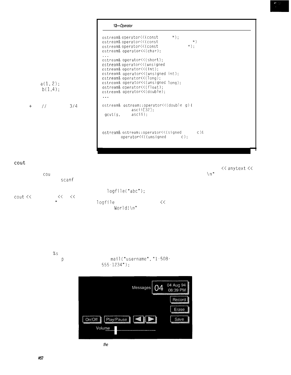
AND ci n
co u t
and c i n are standard stream
controls for C++.
t
and c i n behave
much like pri ntf and
do in C.
YOU
could use it by:
"Hello," 2
"the World!
It prints “Hello, 2 the World!” on
the stream device, which is typically
the monitor. co u t is used prevalently
in C++, although pri ntf and fpri ntf
functions would work as do all of the
other C function library functions. The
advantage is that it is no longer
necessary to embed and %d in the
output statement. Someday, r i n t f
will appear as arcane as punched cards.
c out
is defined as an
Listing
overload redirects stream input or output.
char
unsigned char
signed char
short):
static char
15,
return ascii;
char
return
char)
consider the following. Presume that
an object is defined of type Log. It
should be possible to use overloading
to redirect output to this object:
Log
<< "Hello," << 2
"the
Although device redirection
already exists, a Log object can be used
to record a great deal more state
information about your program.
Finally, consider the same effect with
a Ma i 1 object:
mail << "Hello, Mike:\n\nHere
is my answer"
"signed:
Having established some of the
basics, we need to move on to a more
real-world example.
A (MORE) REAL-WORLD
EXAMPLE
This example is not of a real
answering machine, but is a contrived
example demonstrating design prin-
ciples. Although everyone knows the
basic operation of a telephone answer-
ing machine, converting that knowl-
edge into C++ can prove to be a
challenge for beginners. Like learning
to drive a car, it’s different when you
object of class o s t r e am,
definedin ostream. h in
your favorite compiler. To
support this type of, function-
ality, the << operator must
be overloaded for each
acceptable data type. The
output stream code eventu-
ally calls some code that
converts the received data
type to ASCII (Listing 12).
Arcane and off the point
as
all of this might seem,
Figure I-Code on BBS describes the behavior of this answering machine.
20
Issue
April 1995
Circuit Cellar INK
have to navigate traffic.
A prototype diagram of
an answering machine is
shown in Figure 1. In
addition to the announce-
ment and recording tapes,
the system consists of a
volume slider and the
buttons: On/Off, Play/Pause,
Save, Erase, Record, and
forward/reverse arrows. A
message display shows the
number of messages re-
ceived.
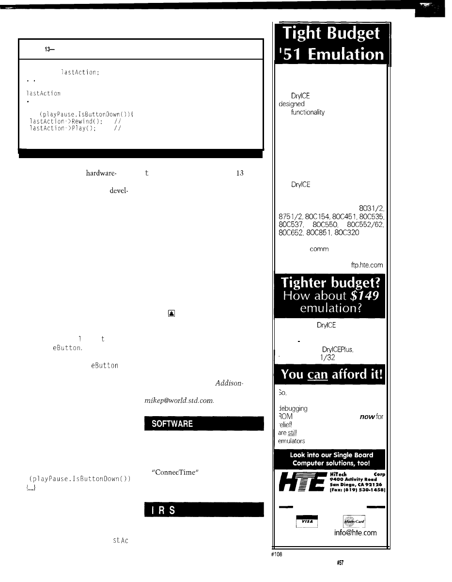
Listing
1 as t
A c t ion is an object reference and can be used to call member functions.
Button
*
= &record;
if
either tape
either tape
problem. So, we’ll just assume that we
Although this is a
independent solution, it is only
can make a function call to either C or
because no hardware has been
assembler that will execute require-
oped-mind you, the 8051 would
ments such as enable recording.
make an excellent chip to solve this
design. I hope this introduction to C++
i on object reference. Listing
helps you understand some basic C++
demonstrates how this is handled.
principles that will eventually moti-
Well-crafted C++ programs give
you a much better sense of the coding
vate you to learn the language.
style and simplistic beauty of the
The code for the system consists
of one main loop waiting for some-
thing to happen such as the phone
ringing or the Play/Pause button being
pressed. An object is defined for a
generic Butt. o n. The purpose of this
object is to perform hardware-depen-
dent functions such as reading the
current button state.
Button is super classed by two
more refined buttons: Ho d B u t o n
and Toggl
The presumption
is that the physical button has only an
up or down state. Toggl
treats the button as if it toggles back to
the up position after its value is read.
It does this by ignoring its physical
state if it hasn’t changed since the last
read.
To read the value on an object
such as a button, you could ask for its
value. However, it may be smarter and
more removed from the physical
environment to ask whether the
button is up or down:
if
The product’s behavior demands
rewinding and replaying either the
greeting or recording tapes depending
on which buttons are pressed. This is
handled by maintaining the 1 a
Finally, both Borland and Micro-
soft have excellent development
systems with integrated environments
that you can play with. But regardless
of what software package you have,
remember there is no better and
quicker way to learn than to just start
coding.
M i k e
Podanoffsky has worked for over
20
years in computers, specializing in
personal computers and database
systems. He is currently working at
Lotus Development on major data-
base products. He is author
of
Dissect-
ing DOS, published by
Wesley. He may be reached at
Software for this article is avail-
able from the Circuit Cellar BBS
and on Software On Disk for this
issue. Please see the end of
in this issue for
downloading and ordering
information.
401
Very Useful
402 Moderately Useful
403 Not Useful
8051
Family Emulator is
truly Low Cost!
The
Plus is
a modular emulator
to get maximum flexibility
and
for your hard earned
dollar.
The common base unit
supports numerous
805 1 family
processor pods that are low in price.
Features
include:
Execute to
breakpoint, Line-by-Line Assembler,
Disassembler, SFR access, Fill, Set and
Dump Internal or External RAM and
Code, Dump Registers, and more.
The
Plus base unit is priced at
a meager $299, and most pods run
only an additional $149. Pods are
available to support the
a n d
more. Interface through your serial
port and a
program. Call for a
brochure or use INTERNET. We’re at
info@hte.com or ftp at
Our
$149
model is what
you’re looking for.
Not an evaluation
board much more powerful. Same
features as the
but limited
to just the 803
processor.
if you’re still doing the
U V
Waltz (Burn-2-3, Erase-2-3). or
through the limited window
emulators give,
call us
Our customers say our products
the
best Performance/Price
available!
Equipment
S i n c e 1 9 8 3
(619) 566-1892
Internet e-mail:
Internet ftp: ftp.hte.com
Circuit Cellar INK
Issue
April 1995
2 1
calling for the high precision and
dynamic range of floating-point
arithmetic, you could use software
emulation in place of an external math
coprocessor.
Software design issues also affect
the performance of the system. Choice
of language, compiler, and memory
model have a direct impact and must
certainly be considered. An even more
important consideration is how well
the software is designed. If it doesn’t
use the most efficient algorithms and
data structures, it could prove to be
one of those applications that brings
even the fastest computer to its knees.
To counteract the dearth of
relevant documentation, this article
offers a detailed look at the perfor-
mance tradeoffs of the Intel ‘186
microprocessor family. Specifically,
we’ll be looking at the Intel ‘186EB
and
which are used for all the
timing measurements. While most of
you likely use a different microproces-
sor family, many of the performance
issues cross architectural boundaries.
With a little imagination, you can
apply these findings to your own
design circumstances.
Rick Naro
Characterizing
Processor Performance
vendors often
provide a great deal of
documentation for their
products. There are data sheets, user
manuals, application notes.. . . Con-
spicuously missing, however, is useful
information on optimizing processor
and system performance.
Even if you design your embedded
system hardware to run flat out and
optimized performance is not a
problem, there are still plenty of
software design issues to consider.
And, if you need to minimize the cost
of a design-who doesn’t in a
volume embedded
understanding the relationship
between the CPU bandwidth, memory,
peripherals, and software development
tools is key to success.
The choices of cutting perfor-
mance to achieve a lower design cost
are many. You might vary the size of
the microprocessor external bus paths
to eliminate devices. You could add
wait states and use slower memory
BUS BANDWIDTH
The Intel
consists of
microprocessors with
internal data paths. However, when
the first family members were intro-
duced, Intel prepared two
the 8086 and the 8088.
For those who remember back to
198 1 when IBM was designing the first
PC, you may recall that IBM made a
conscious choice to use the 8088. Its
use of an
external bus reduced
hardware costs. Little has changed
since then. You still have a choice of
‘186 and ‘188 family members where
the only difference is the use of
or
external data paths.
As in 1981, a system designed
around the ‘188 is less expensive since
devices which cost less
than higher-speed
devices. You could run
the system clock at a
nonstandard frequency,
perhaps saving the need
Table l--Even though the
bus of the ‘188 is only
as
wide as the
for an additional crystal
bus on fhe ‘186, the former achieves better than 60% of the /after’s
oscillator. In applications
performance. Both systems are
in other aspects. times are
milliseconds.
22
Issue
April 1995
Circuit Cellar INK
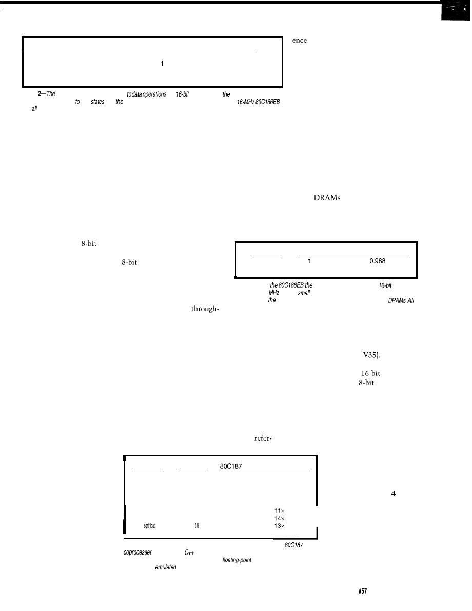
EPROM Wait States
RAM Wait States
Execution Time Relative Performance
0
0
17.965
1.000
0
1
8.748
0.958
1
0
20.157
0.891
1
1
20.968
0.857
Table
high ratio of instruction fetches
in a
system shows EPROM address
space is more sensitive waif
than RAM address space. Tests were performed on a
and
times are in milliseconds.
only half the number of memory
devices (EPROM and RAM) are
required. Further savings are gained by
eliminating the extra data bus buffer.
If things were simple, we might
expect the ‘188 to be exactly one half
the speed of the ‘186 because of having
half the bus bandwidth. But even back
then, Intel built parallel CPU and bus
interface units into the devices,
complicating analysis. By running
some test code on both processors, we
can roughly determine the penalty of
designing with an
external data
bus (see Table 1).
eral device. Normally, you want to run
with zero wait states since this
maximizes the system performance.
But, in systems where excess band-
width is available, designing in slower
devices and inserting wait states is an
acceptable compromise to reduce the
cost of the system.
Since there are at least two
distinct address spaces, the question of
where to insert the wait states comes
up. We can use the EPROM address
space for code and
This result shows that the
external version has nearly two thirds
of the performance of the 16-bit
version, which is considerably more
than my initial speculation. Besides
the separate CPU and bus units, both
the ‘186 and ‘188 use an instruction
queue to prefetch instructions-six
bytes for the ‘186 and four bytes for
the ‘188. On the surface, this seems to
bias the results toward the ‘186
because of more instruction queue
hits.
constant data and
the RAM address
space for read/write
data and the stack.
To determine which
option is better, we
Table 3-Using
effect of DRAM refresh on a
system
need to know the
running at 16
is quite
Whether or
not fhe DRAM is used in a system is
determined by additional hardware cost of supporting lower-cost
impact on
times are in milliseconds.
put by inserting wait
states separately into each address
space and measuring the result.
Memory devices can then be chosen to
deliver a specific level of performance
while reducing the memory device
cost.
The solution to the problem lies
in the bus bandwidth used rather than
the available bandwidth. In the case of
the ‘186, the bus interface unit is
sitting idle more than 30% of the time
while the ‘188 is chugging away at
while the
over 90% bus utilization. So,
‘186 bus unit is sitting idle,
the ‘188 is busy catching up.
Add more bus usage through
DRAM refresh cycles, DMA
cycles, and external bus
masters, and the 16-bit
external bus looks like a
much better solution for
higher-end systems.
From Table 2, it is clear that the
penalty for adding wait states to the
RAM address space is only half that for
EPROM address space. These findings
make sense since the processor is
constantly executing instructions, but
not every instruction makes a
Operation
Emulation
Relative Performance
perform refresh on a
Add float
226
17
13x
Add double
241
23
10x
frequent basis. For instance,
Multiply float
275
17
16x
typically,
there are 256
Multiply double
292
23
13x
refresh cycles every ms.
Divide float
287
21
14x
As you can see in Table
sin(float)
Divide double
306 977
27 68 41
MEMORY WAIT STATES
Wait states are used to
match a fast processor with
a slower memory or periph-
to the data address space. With
this knowledge, it becomes possible to
optimize the wait states for each
address space in the system with the
cost and benefit known in advance.
DRAM REFRESH
We can also use dynamic RAM
since we know the cost per bit is
much less than for static RAM of the
same density. For this scenario, we
need to find the impact on perfor-
mance of adding the additional refresh
bus cycles to the normal mix and see
what effect this has on the system.
While DRAM refresh has a low
impact on the throughput, the lower
cost of
must also be weighed
against higher design costs associated
with the additional hardware needed
for RAS/CAS generation and timing.
Processor
Execution Time
Relative Performance
Refresh enabled
a.085
Refresh disabled
17.867
1.000
Some microprocessor vendors have
recognized this and have optimized the
external bus for a direct DRAM
connection (e.g., NEC
From my experience with bus
utilization, I expect a
bus to be
affected less than an
bus. A 16-bit
bus has more idle bus bandwidth that
can be handed over to the refresh
controller without any impact on
performance.
Still, there will be some impact
since DRAM-refresh bus cycles have
priority over other bus
cycles and we need to
I
3, the penalty for DRAM is
not bad, but there is one
caveat to consider. The
Table 4-Here are common floating-point operations executed using an
math
refresh overhead is fixed by
and Borland’s
4.5 mafh coprocessor emulation. While hardware wins
the DRAM memory devices
hands down, applications performing limited
arithmetic can be we//-
and is independent of the
served by fhe
variety. All times in microseconds.
microprocessor. As you
Circuit Cellar INK
Issue
April 1995
23

slow the processor down or
reduce the available bus
bandwidth, the same
number of refresh cycles
must be performed in the
same refresh interval. So, if
YOU
cut vour bus
Table B-These are the most common
real-mode
models encountered
width, expect to see the
in a real-mode
PC or compatible. Tiny and huge memory models are left out as
overhead of DRAM refresh
being unnecessary for the typical embedded system.
increase.
FLOATING-POINT
PERFORMANCE
Although the cost of floating-point
hardware continues to drop, the
decision to add a hardware math
coprocessor is still an expensive
proposition in any design. The alterna-
tive is software emulation of the math
coprocessor. While this is more cost
effective, it requires the availability of
excess CPU throughput to take over
from the missing hardware.
On the surface, the high floating-
point penalty may appear insurmount-
able, but in the real world, an embed-
ded controller doesn’t spend anything
close to 100% of its time on floating-
point calculations. To decide if a
software coprocessor can meet the
system requirements, we need to
The penalty for having
a large code address space is
insignificant. But, the large
data address space costs 5%
of the total bandwidth.
The moral of the story
is to stick to the small or
medium memory models.
outside this article’s scope, let’s look
at what we can control.
The Intel 80x86 microprocessors
are famous (or infamous) for their use
of segmented address space. Compil-
ers, such as Borland C++, support a
variety of memory models depending
on the need to access 64 KB or
1
MB of
the code and data address spaces. For
those not familiar with the Intel
architecture, four memory models are
common. As you can see from Table 5,
there are differences a design can
exploit.
Use far pointers selectively when
access to more than 64 KB of data is
required.
UNDERSTANDING
INTERRUPT LATENCY
Recall in the section on memory
wait states, we saw that the EPROM
address space was more sensitive to
wait states than the RAM address
space. But, unlike wait states, the
overhead for a
1
-MB code address space
is only limited to the CALL and RET
Interrupt latency involves the
delay in responding to an event and
has several components-the time to
complete the current instruction, the
time to save the processor state on the
stack, and the time to get to applica-
tion code where the interrupt is finally
serviced. The balance of the time spent
servicing the interrupt is the interrupt
service time.
Although the first two delays are
out of our hands, the time it takes to
get in and out of the interrupt service
routine is ripe for optimization. It is
important to know just what the
Memory Model
Small
Medium
interrupt latency of a
level language is so you can
Execution Time
Relative Performance
16.807
1.000
decide if an assembly
16.905
0.994
guage routine improves
reflect this additional
overhead.
know the difference in
performance between the two
implementations using the
most common floating-point
operations.
In addition to the
comparisons between the
floating-point operations in
Table 4, it would help to
know how much slack CPU
Compact
17.735
0.948
Large
17.869
0.941
Table
the relative performance of the same application in each
memory mode/ on a
system, the largest performance penalty comes from
the use of far data pointers. times are in milliseconds.
performance.
Modern compilers like
Borland C++ and Microsoft
Visual C++ perform a great
deal of optimization. But both
compilers always push the
entire processor state on the stack,
even if only a fraction is actually used.
is available. A system running near
full capacity is not a candidate for a
software emulation. However, some-
times spending money on a faster CPU
and more memory to increase the
available throughput to handle the
software emulation can be the winning
strategy that results in overall
cost reduction.
COMPILER MEMORY MODEL
Enough on hardware! What about
software design decisions that affect
application performance?
Of course, the biggest contributors
to efficient software are algorithms
and design. Since these issues exist
instructions using the longer segment
and offset formats. However, predict-
ing the behavior of the data address
space is another matter and is ham-
pered by complexity.
Local variables allocated in
registers or on the stack are always
accessed without penalty as is most
statically allocated data. The penalty
arises when far pointers are used. Not
only are more pushes and pops
required to pass parameters, the actual
accessing of the data also takes longer
with the need to load a segment
register. From Table 6, we can see that
the results of running the same
application in each memory model
On the test ‘186EB system, a C++
interrupt handler with a single I/O
command takes a total of 15.4 to
execute. the same code is rewritten
in assembly language, the time can be
reduced to just 7.7
It is worth
noting that the assembly language
advantage is temporary. More complex
interrupt handlers require you to save
more of the processor state, which
eventually equalizes the overhead.
Still, in my opinion, great assem-
bly language programmers have an
edge over the compiler in writing
optimized code.
2 4
Issue
April 1995
Circuit Cellar INK
HEAP PERFORMANCE
Many embedded-system
developers try not to think about
heaps. They avoid them as much
as possible due to their
run-time requirements.
While fixed-size allocation speeds
up the time required to allocate
and deallocate memory, the
hottest trend toward
oriented programming in embedded
systems
is likely to force programmers
to consider the effects of heaps.
Unlike C, C++ includes dynamic
memory allocation in the language
specification, so it is difficult to avoid.
While it is possible to create a C++
application using only statically
allocated objects or objects created on
the stack, knowing that the new and
delete operators are available solves
some thorny development issues. If
you plan to use these functions, it is
best to know in advance what the best,
worst, and average times for
based objects is.
For a simple test, you can allocate
and delete array objects from the heap
in a random fashion, measuring the
overhead over a period of time. Based
on this information, the software
design optimizes performance by
time-sensitive memory
and lets the noncritical code take
advantage of the efficiency of dynami-
cally allocated memory. To test
system performance, 500 blocks of
random size are randomly allocated
and released.
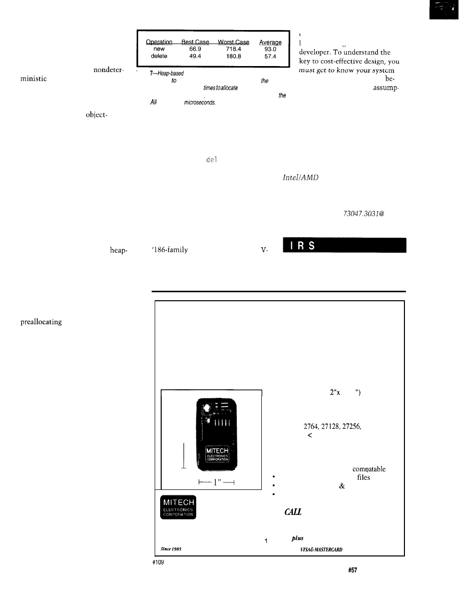
From the results in Table 7, it
appears that freeing up dynamically
allocated memory is more efficient.
This is as it should be since the block
size plays no role, unlike when the
block is first allocated. While the new
operator’s average behavior is not far
from the best-case behavior, its worst
case sticks out like a sore thumb.
While one may not be able to
avoid a heap, it certainly is possible to
live with one. Third-party replace-
ments for the Borland and Microsoft
dynamic memory management
packages are available with options for
fixed-size allocation, multiple heaps,
and the ability to catch heap errors.
Even the C++ language recognizes that
you might not be able to live with the
enough that they can benefit any
hardware designer or software
Table
dynamic memory allocation is not exact or
predictable due the use of/inked lists. Shown here are
best,
components inside and out
worst, and average
execution
and free memory in a
Ctt
application which randomly allocates and frees objects from
fore making any design
tions. That way, both wild and
heap. times are in
educated guesses can be trans-
formed into sure bets. And, the
resulting design will certainly be a
success.
q
default memory allocators, so they
offer a custom memory allocator more
suitable for a real-time system. As a
last resort, you can simply avoid the
use of the new and
et e operators.
PUTTING IT ALL TOGETHER
I covered many of the most
accessible hardware and software
optimizations that impact system
performance. Unfortunately, the
specific data provided may be of little
use unless you’re one of those lucky
souls designing with Intel and AMD
processors or the NEC
series microprocessors.
Nonetheless, the design optimiza-
tion techniques are general purpose
Rick Naro is president of Paradigm
Systems, a developer of embedded
system development tools for the
186 and NEC V-series
microprocessors. In the past, he
designed hardware and wrote applica-
tions for embedded 80x86 systems. He
may be reached at
compuserve.com.
404 Very Useful
405 Moderately Useful
406 Not Useful
OUR SMALLEST
EPROM EMULATOR
Eliminate the need to burn and learn
all in a package about the size of a 9 volt battery
l
Super
small (about
1 “xl
T
2”
411
Washington Street,
Otsego, Michigan 49076
TEL: 616-694-4920 FAX: 616-692-265
l
Uses Surface Mount Design
l
Fits in EPROM socket
l
Downloads in less than 7
seconds
l
Emulates
275 12
l
Access time 1 OONS
l
Plug and Play: Plug cable into computer
and download. Once power is supplied to
circuit, cable can be removed
l
Includes software for IBM
PC’s
Loads Intel Hex and Binary
Includes Serial Cable Battery Backup
Nearly same footprint as EPROM
NO Wfor Your Special
Introductory Price of $194.95
$5.00 shipping and handling
ACCEPTED
Circuit Cellar INK
Issue
April 1995
2 5
Designing
with
04
Rick Lehrbaum
ver
the past ten
years, the IBM
compatible architec-
ture has become an
increasingly popular platform. In
addition to their typical use as dedi-
cated desktop computers, they’ve
reached into the embedded world.
They’re now being used in embedded
microcomputer applications such as
vending machines, laboratory instru-
ments, communications devices, and
medical equipment. PCs are beginning
to be found everywhere!
THE TREND TOWARD
EMBEDDED PCS
From a computer architect’s
perspective, the PC architecture with
its 808%based origins and inherently
segmented world view is hardly
something to get excited about.
Why, then, turn the world’s
favorite
desktop
system into an
embedded
microcomputer standard?
not just keep using a
or
Regardless of its particular
implementation-from and
single-chip microcontrollers to
performance,
RISC
embedded microprocessors are simply
a means to an end-not an end in
themselves. After all, the purpose of an
embedded microcomputer is to run the
application software. It’s the software,
not the embedded computer, that
makes the application what it is. As
long as it can run the application
software acceptably, the ideal embed-
ded computer is one that minimizes
risks, costs, and development time.
Development cost is the major
reason for shying away from a multi-
plicity of microprocessors since their
architectures vary greatly. Each
requires new development tools,
including emulators, compilers, and
debuggers. And, every time you use a
different microprocessor in a system
design, you’ll invest thousands of
dollars and weeks of time putting the
development environment in place.
No wonder system developers seek
alternatives to using the latest new
microprocessor in every new project.
Also, it’s common for old projects,
based on older microprocessors, to
Photo
modules are compact, rugged, and self-stacking.
three module stack measures just
yet it
contains fhe equivalent functions of a complete desktop PC: a PC/AT motherboard, up to of
DRAM,
parallel interfaces,
LAN controller,
display
and a bootable
disk drive.
26
Issue
April 1995
Circuit Cellar INK
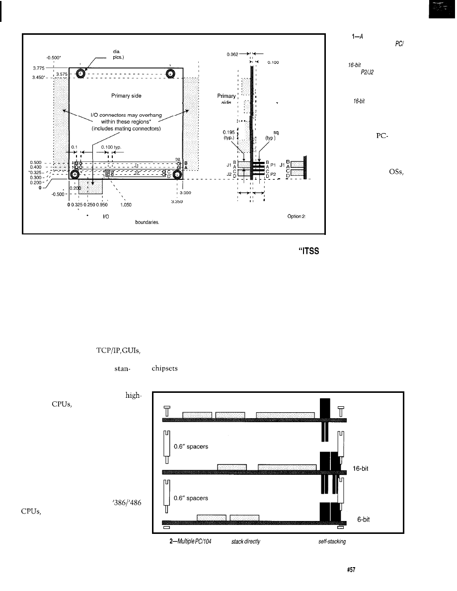
0.250 dia. pad
0.125
hole
0 . 3 5 0
(4
3 . 2 5 0
4 0 5 0
0.100 typ.
0.100 typ.
Secondary
side
I
0 . 0 2 5
J2
‘ 0 . 4 3 5 0 . 4 2 0
NOTE:
mating connectors may not
Option 1:
extend outside these
Stackthrough bus
Non-stackthrough bus
become difficult or even impossible to
maintain, as familiarity with the older
architectures and their development
tools fades.
All this has stimulated a desire for
hardware and software standards. On
the software side, this means using C,
C++, and object-oriented programming
methods. Programmers increasingly
rely on familiar software environments
such as UNIX, DOS, or Windows, and
interface standards like
and so on.
But what about hardware
With over 200 million desktop PCs in
use worldwide and nearly a million
new ones sold each week, the PC
architecture has been dubbed the
Industry Standard Architecture
(ISA).
This is why the PC architecture is
gaining increasing acceptance as an
embedded microcomputer standard.
Using an embedded-PC architecture
leads to significant savings in develop-
ment time and money. PC develop-
ment tools are plentiful, cost-effective,
and easy to use. PC-compatible
and peripherals are abundant.
Figure
dimension
drawing, extracted from fhe
104 specifications, shows the
detailed mechanical dimensions
of the
PC/l 04 module
format. The
connector is
not required on d-bit modules,
but may be included as an
option to provide “pass through”
of a
full
bus.
documented.
oriented software
components are
readily available and
include real-time
drivers, function
libraries, and applica-
tion programs.
Hardware engineers
know the PC’s bus
and programmers, its
software.
THE
PRINCIPLE”
In short, the reason so many
embedded system developers are
migrating to the PC architecture lies
not in the hardware, but in the
software. This trend has inspired the
ITSS principle, a new “law” of embed-
ded system engineering, which stands
for It’s the software, stupid!
MAKING THE PC FIT
One potential problem with using
the PC architecture in an embedded
system is that standard PC subsystems
dards? Unfortunately, the tremendous
Their functions are familiar and well
don’t meet the more stringent size,
diversity of microprocessor architec-
tures, from the lowly 8051 to the
end RISC
has prevented the
emergence of any real standards for
Stackthrough
8-bit module
embedded-system hardware. Only the
industrial computer buses such as
VME, Multibus, and STD provide a
measure of consistency. However,
their use is limited to systems which
are larger and more complex (and
Stackthrough
module
therefore less cost-sensitive) than most
typical embedded systems.
On the other hand, the highly
multisourced PC-compatible
chipsets, and associated
peripherals have made the PC architec-
ture attractive as a cost-effective
hardware platform for low- and
medium-performance applications.
Non-stackthrough
1
module
Figure
modules
on top of each other using
pin-and-socket bus
connectors. Four spacers rigid/y attach each module to the one above and below it.
Circuit Cellar INK
Issue
April 1995
27
power, ruggedness, and reliability
requirements of most embedded
applications. This is natural since PCs
are optimized for the highly
sensitive desktop personal-computing
market.
But, you can avoid this problem by
designing a custom, chip-level embed-
ded PC directly into the embedded
system’s hardware. This way you can
take advantage of PC chipsets, compo-
nents, and software in an embedded
environment.
The trouble with this approach is
that it doesn’t eliminate many of the
costs and risks you want to avoid by
using an off-the-shelf PC architecture.
You still end up designing and debug-
ging a CPU subsystem, licensing and
porting a BIOS, and in many other
ways needlessly reinventing the
wheel.
Although PC/l 04 modules have
been around since 1987 (in the form of
it was not
until
released a formal specifi-
cation to the public domain in 1992
that interest in
skyrocketed.
Since then, hundreds of
modules have been announced by the
more than 140 members of the
nonprofit PC/ 104 Consortium. In
1994,
achieved a significant
milestone when Intel endorsed it as a
recommended way to expand designs
based on Intel’s new embedded ‘386
In 1992, a working group of the
IEEE embarked on a project to stan-
dardize a small form-factor version of
the PC/AT bus, which was also based
on
The new IEEE “P996.1”
draft standard, which conforms closely
Since standard PC
subsystems aren’t
suited to the targeted
environments, the desire
to use PC architecture in
embedded systems thus
contains an inherent
contradiction. This is
what inspired the
creation and rapid
acceptance of the PC/
104 embedded-PC
modules standard (see
Photo 1).
WHAT IS
offers full
hardware and software
compatibility with the
standard desktop PC
(and PC/AT) architec-
ture, but in an
compact (3.6” x
self-stacking, modular
form.
defines a
standard way to repack-
age desktop PC func-
tions for the ruggedness
and reliability con-
straints of embedded
systems. Consequently,
offers an
attractive PC-compatible
alternative to traditional
microprocessor-based
embedded systems.
to
specification, is now
approaching IEEE approval.
WHAT’S IN THE
STANDARD?
As mentioned above, the key
differences between
and the
normal PC hardware standard are
mainly mechanical. Instead of the
usual PC or PC/AT expansion card
form-factor (12.5” x
each
module’s size is reduced to approxi-
mately 3.6” x 3.8”.
Two bus formats for and 16-bit
modules are provided. However,
unlike the and
versions of the
normal PC bus, and 16-bit
modules are the same size. Figure 1
shows the detailed mechanical
dimensions of the
module format. An
module has
Pin
Number
Row A
Row B
Row
Row D’
0
o v
o v
1
o v
2
SD7
RESETDRV
LA23
3
SD6
v
LA22
4
SD5
LA21
5
SD4
-5 v
LA20
6
SD3
DRQ2
LA19
IRQ15
7
SD2
-12 v
LA18
8
SD1
ENDXFR*
LA17
DACKO*
9
MEMR’
DRQO
10
(KEY)*
11
SMEMW
SD8
DRQ5
12
SD9
13
SA18
SD10
14
SA17
SD1 1
15
SA16
SD12
DRQ7
16
SA15
DRQ3
SD13
v
17
DACKl*
SD14
MASTER*
18
SA13
SD15
o v
19
SA12
REFRESH*
(KEY)*
o v
20
1
SYSCLK
21
22
23
SA8
24
SA7
25
SA6
26
SA5
27
SA4
TC
28
SA3
BALE
29
SA2
v
30
o s c
31
SAO
o v
32
o v
o v
NOTES:
Rows C and D are not required on
modules, but may be included.
2.
and Cl9 are key locations.
Table
names comes from the use of 104 bus signals. Each
bus
equivalent a corresponding signal of the normal PC/AT bus.
no
bus connector.
To eliminate the
complexity, cost, and
bulk of conventional
motherboards, back-
planes, and card cages,
modules
implement a
stacking (also referred to
as
stackthrough)
bus
connector. Multiple
modules are stacked
directly on top of each
other without additional
bussing or mounting
components. Four nylon
or metal spacers
in
length] are normally
used to rigidly attach
the
modules to
each other as shown in
Figure 2.
Rugged and reliable
and
male/female header
connectors replace the
standard PC’s
and
36-position
and
edge-card bus connec-
tors. The
bus
connectors feature two
pin-and-socket rows on
0.1” centers and nor-
mally have gold-plated
contacts. Both Samtec
and Astron, two
connector companies,
28
Issue
April 1995
Circuit Cellar INK
currently offer alternate
sourcing of the approved bus
connectors.
PC/IO4 bus signals are
functionally identical to their
counterparts on the PC/AT
bus. Their assignments to the
104 positions on the
header-bus are listed in Table
1.
To reduce power con-
sumption to around
l-2
W per
module and minimize chip
count, the bus drive was
reduced from the normal PC’s
24
to 4
This permits
or equivalent
Figure
schematic shows a
means of implementing the
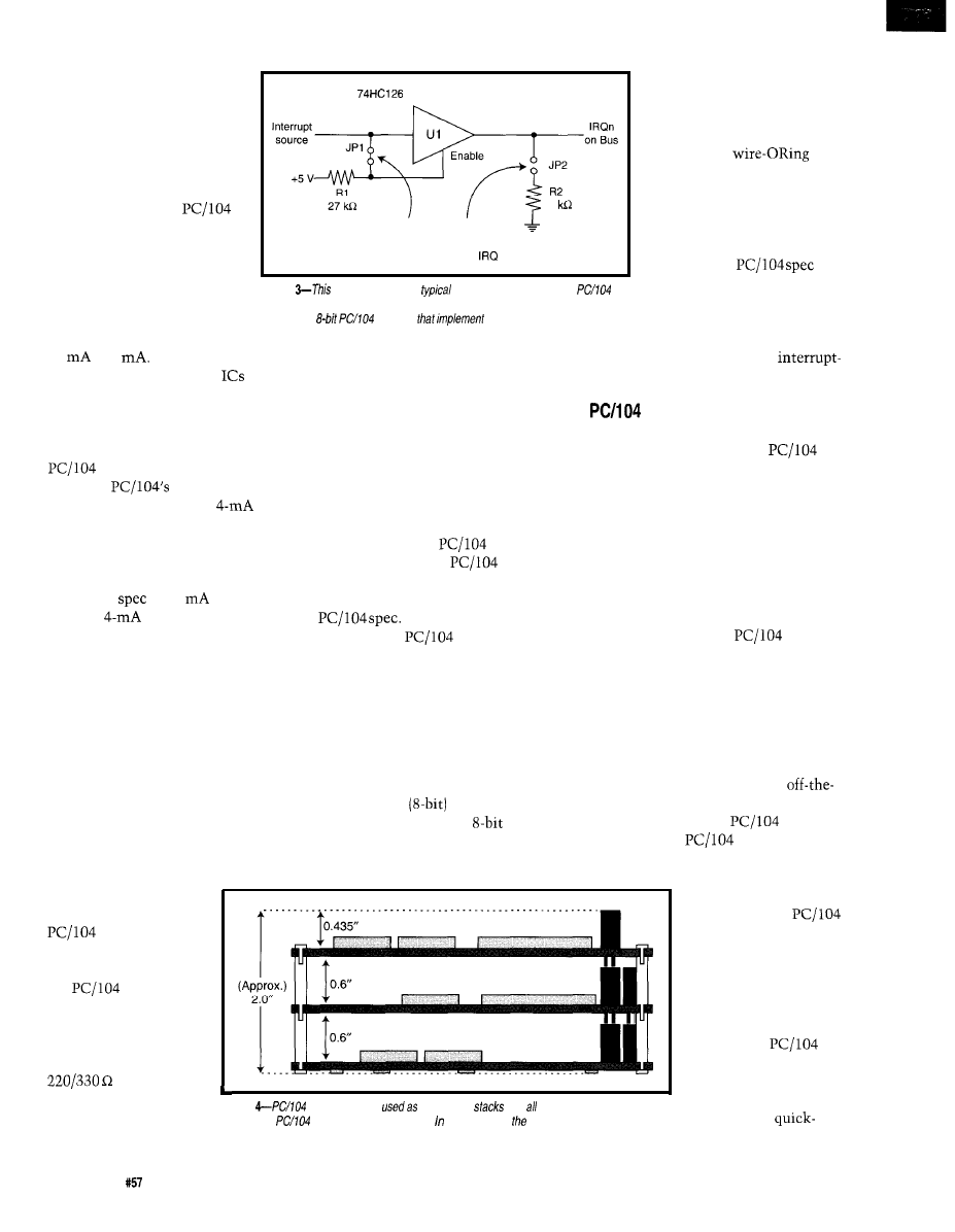
bus interrupt-sharing option. While interrupt sharing is not required, if is frequently
provided by
modules
communications and
nefworking functions.
an option, as well. If
you plan to terminate a
bus, be sure to
use the AC method of
termination defined in
the
specifica-
tion rather than pure
resistive termination.
Plain resistive
termination, usually
between
each signal and ground,
exceeds available bus
current. On the other
1
Remove jumper
Install jumper
for normal P996
on one device
bus operation
per
HCT logic and many VLSI
to
directly drive the bus without addi-
tional buffer chips.
Many developers wonder how
many modules can be used on a single
bus. The answer is not simply
related to
reduced bus drive
current. Actually, the low
drive
does not result in a small number of
permissible bus modules. For most
embedded systems, there is plenty of
bus drive. In fact, since the maximum
input load
is 0.4
per bus
signal, a
bus drive current can
theoretically handle ten bus loads!
In practice, factors such as signal
trace lengths and connector impedance
transitions limit the number of
modules you can reliably use to
between six and eight. The actual
limit, for a particular system, depends
on total bus length, number of stacked
connectors, environmental issues, and
the specific modules used. Also don’t
forget to consider voltage drops on the
bus power signals due to multiple
stacked modules.
Bus termination is
3 0
Issue
April 1995
Circuit Cellar INK
hand, the recommended AC termina-
tion consists of a series R/C network
between each signal and ground. This
approach draws no static current and
provides a better impedance match for
the bus.
If you’re not sure whether or not
termination is needed in your system,
it’s best to provide a way to add it
later. A number of
vendors
offer special plug-in
termina-
tors, which provide the method of AC
termination recommended by the
These terminators can be
added at any
bus stacking
location. You can also include posi-
tions for tiny SIP termination net-
works directly on PC/ 104 modules or
interfacing boards you design.
When you use the PC architecture
in embedded applications, it’s not
uncommon to run out of bus interrupt
channels. This is especially true of
byte-oriented
interfaces such as
serial ports because the
subset of
the PC bus contains six interrupt lines,
standardized system func-
tions. Unfortunately, since
the bus interrupt lines are
active high, the common
technique of
multiple interrupt requests
on a single-interrupt input
line (used with other buses) is
not possible.
To circumvent this
problem, the
includes a recommended
means for multiple interrupt-
ing sources (on one or more
modules) to share a single bus
interrupt. A sample
sharing circuit appears in Figure 3.
IN REAL APPLICATIONS
Although configuration and
application possibilities for
modules are practically limitless, there
are a few ways the modules tend to be
used in actual embedded systems.
l
Stand-alone module stacks
As illustrated in Figure 4, stacks of
PC/l 04 modules can be used like
ultracompact bus boards, but without
the usual requirement for backplanes
or card cages. Often, a
module
stack is bolted somewhere inside the
embedded system’s enclosure in a
convenient location that would
otherwise simply be dead space. In this
manner, an entire PC can be embedded
directly within a system that would
otherwise require an external PC.
There are also a variety of
shelf PC/ 104 stack enclosures that
host from three to six
mod-
ules. Enclosed
stacks like
most of which are dedicated to
these can be self-contained systems or
can be used as sub-
systems within larger
systems. These
system enclosures are
designed for a variety
of environments
(commercial, indus-
trial, and vehicular)
and are available with
options like
form-factor power
supplies (for 8-80-V
AC/DC inputs), shock
mounts, and
release mechanisms.
Figure
modules can be
stand-alone
with required system functions
provided by
modules stacked together. fhis approach, modules function like a
miniaturized backplane bus.
l
Macrocomponent applications
In Figure 5, another common
method of using
is shown.
Here it is used as macrocomponents
that plug into a custom,
specific baseboard. The
baseboard typically contains all
interfaces and logic that aren’t avail-
able (or desirable) on the
modules. Typically, the baseboard
includes power supply components,
signal conditioning, external
connectors, and so on.
What’s interesting about the
macrocomponent approach is instead
of plugging the I/O into the computer,
you plug the computer into the I/O!
It’s a new embedded-system paradigm.
This approach lets you focus more
energy on the application’s unique
requirements, and less on
a basic (micro) computer architecture.
With this approach, the system
becomes a hybrid of out-sourced
modules (the
modules) plus a
custom-designed board (the baseboard).
Often, the baseboard provides
multiple
stack locations. This
means that the modules can be
distributed horizontally, thereby
keeping a low profile so there’s room
for upgrades and expansion in the
future. Whenever possible, leave extra
vertical space (at least 0.6”) so the
module’s self-stacking bus can
be used for future upgrades and
options. This space also provides room
for temporary addition of modules for
system debug, test, and service.
The shape and size of the base-
board is completely arbitrary. The
baseboard typically takes the shape of
the desired end system, so its shape
can be anything-square, round,
rectangular, customized.
l
Mezzanine bus applications
A third and increasingly common
way for
modules to be used is
as I/O expansion daughter modules on
PC-compatible single-board computers
This approach, known as a PC/
mezzanine bus,
is now found on
nearly every new PC-compatible SBC,
including both stand-alone (proprietary
form-factor)
and passive back-
plane (PC-expansion-card form-factor)
industrial PCs.
Real-time Emulators
RICE16 and
real-time in-circuit
emulators for the
and
family microcontrollers:
affordable, feature-filled development systems from
Retail for
RICE16 Features:
Real-time
Emulation to
for
and
for
PC-Hosted via Parallel Port
Support all oscillator type5
Program
Memory
by
24-bit real-time Trace Buffer
Level Debugging
Unlimited Breakpoints
Emulators for
External Trigger Break with either
“AND/OR” with Breakpoints
Trigger Outputs on
Address Range
12 External Logic Probes
User-Selectable Internal Clock from
40 frequencies or External Clock
Single Step, Multiple Step, To Cursor,
Step over Call, Return to Caller, etc.
On-line Assembler for patch instruction
Easy-to-use windowed
available now!
n
Support
and
with
Optional Probe Cards
n
Comes Complete with
Macro
Assembler, Emulation Software, Power
Adapter, Parallel Adapter Cable and
User’s Guide
30-day Money Back Guarantee
n
Made in the U.S.A.
RICE-xx Junior series
RICE-xx “Junior” series emulators support;
family,
or
They offer the same real-time features of RICE16 with the
respective probe cards less real-time trace capture. Price starts at $599.
PIC Gang Programmers
Advanced Transdata Corp.
offers PRODUCTION QUALITY
gang programmers for the different PIC microcontrollers.
n
Sand-alone COPY mode from a master device
n
PC-hosted mode
for single unit programming High throughput Checksum verification
on master device Code protection Verify at
and
Each
program cycle includes blank check, program and
eight devices
n
Price5 start at
for
family
for
Call (214) 980-2960 today for our new catalog.
and
other
demos,
call our
at (214) 980-0067.
Advanced Transdata Corporation
Tel
Midway Road. Suite 128. Dallas,
75244
Fax (214)
Circuit Cellar INK
Issue
April 1995
31
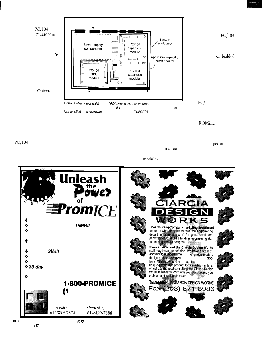
OBJECT-ORIENTED
HARDWARE
Using
modules as
ponents parallels the
object-oriented software
methods of most of
today’s programmers.
object-oriented soft-
ware, the program is
broken into building
blocks which are
separately specified,
developed, tested, and
maintained.
oriented software
greatly reduces the risks
and complexity of
Power
connector
Rear-panel connectors
Front-panel controls
l
users or
macrocomponents,
plugged into an application baseboard. In approach, the baseboard usual/y contains
sottware development
and accelerates project
schedules while
are
specific application, and
modules provide standard
PC
system functions such as CPU, mass storage, networking, communications, and display
interface.
based approach to
embedded system design
that can help you make
the most of using
modules.
Make the PC archi-
tecture a macrocompon-
ent. The entire
PC architecture can be a
single plug-in component,
including all motherboard
functions, system RAM,
memory, and BIOS. You
shouldn’t need to be
concerned with licensing
or modifying a PC BIOS.
Your
04 CPU
module can include a
solid-state disk, so you
also don’t have to worry
about
your
producing more powerful, feature-rich,
and maintainable application software.
are completed faster, at lower budgets,
embedded application’s code.
Similar benefits are realized when
with enhanced features, and are
Let variable performance work to
CPU and I/O macrocompon-
considerably easier to maintain.
your advantage. Projects frequently
ents are used as the building blocks of
MAKING THE MOST OF IT
end up needing more CPU
object-oriented hardware. And, you
than originally anticipated.
experience similar rewards-projects
There are some techniques of
When this happens, be prepared to
exploiting an object-oriented,
unplug the PC/ 104 CPU module
Connect via ROM Socket; DIP; PLCC; SMT
Emulate ROMs up to
in Size
Fastest Downloads Available:
Parallel; Serial; Ethernet
Run Industry Standard Debuggers
l :* Target Processor Independent
Support
Targets
Host Software Sources Included
Shielded Cables for Reliable Operation
Money-Back Guarantee;
1 Year Warranty!
Unlimited Phone Support; 24hr BBS
Call Today
-800-776-6423)
Grammar Engine Inc.
921
Dr., Suite 122
OH 43081
l
Fax
rs and
to
tricky engineering
an
solution for a
See us at Embedded Systems East booth
3 2
Issue
April 1995
Circuit Cellar INK
you’re using and replace it with a
broad range of CPU types and
faster one. Can you imagine doing this
with an 8051,
or a discrete
Allow for performance and feature
options and upgrades. No doubt,
Also, keep in mind the option of
you’ve been in the position of having
kick-starting a project by initially
to provide both high performance and
using a faster
CPU module
low cost within one design. Now, you
than required to get the application up
can provide both by offering multiple
and running quickly. Later, you can
price and performance options. In a
cost reduce by optimizing the software
system, a single base
and substituting a slower (and less
design supports multiple feature or
expensive) CPU module.
cost configurations. You can offer ‘486
To anticipate these possibilities,
performance at the high end and 8088
select
CPU modules that are
economy at the low end. You can
members of a CPU family offering a
provide a wide variety of
by
J. Labrosse
Embedded Systems Building Blocks, Complete and
Ready-to-Use Modules in C contains software modules
you can use to design embedded systems and explains
how to use these modules and modify them as needed.
Labrosse orovides hiahlv
code
for many common
keyboard scanning,
display interfaces, timers and clocks, discrete
analog
and serial communications. Labrosse
provides basic building blocks for all these processes
freeing you to work on the fun and unique parts of your
designs.
R&D Publications, 1995, 620 pp.
O-13-359779-2
V74 with disk. . . .
by Jean J. Labrosse
This book explains the design and implementation of the
Micro-Controller Operating System, a portable,
preemptive, real-time, multitasking kernel for
microprocessors. The system is written in C with
assembly language code for the target microprocessor
kept to a minimum. It can be ported to any
microprocessor that provides a stack pointer and allows
the CPU registers to be pushed onto and popped from
the stack. The system can manage up to 63 tasks, with
performance comparable to many commercially
available kernels. The text explains the fundamentals of
multitasking real-time systems, details the design
decisions of this kernel, and includes a user’s manual for
the system.
R&D Publications, 1992, 266 pp.
0-13-031352-l
W62 with disk. . . . . $54.90
tions options based on
serial,
modem, Ethernet, or even wireless
LAN plug-in modules.
Take advantage of sophisticated
PC functions. In contrast to traditional
microcontroller-based designs, your
system design can draw
on a rich set of PC technologies. Your
designs need not be limited by what
you can do yourself!
Here are some readily available
options:
l
user-friendly graphical user inter-
faces
instead of character or
LED displays
l
popular mass storage devices (floppy,
IDE hard disks, SCSI drives, or
PCMCIA cards with
system support software instead of
ROM or battery-backed RAM
l
full-function
(Ethernet,
Token Ring) instead of
slower RS-232 or RS-485 multidrop
interfaces
l
various SCSI or PCMCIA devices
l
a wide range of off-the-shelf, applica-
tion-oriented
modules
(digital and analog I/O, motion
control, etc.) complete with
to-use PC-compatible software
drivers
Maximize system life expectancy.
A system based on
modules
has a longer life span than that of a
traditional monolithic embedded
system. Some of this longevity stems
from the fact that when a monolithic
system design no longer meets the
requirements of its users, you may be
faced with a redesign.
On the other hand, with a
based system, it is often possible to
upgrade the system to a higher
performance CPU, faster or alternative
peripheral interfaces, and enhanced
software. Thus, a
system design might survive two or
three times longer than a monolithic
one.
If you must replicate or service a
particular design over several years,
the risk of component obsolescence
becomes an important issue. Mono-
lithic designs are in trouble when one
of the chips used in the system is no
longer offered by its manufacturer.
Circuit Cellar INK
Issue
April 1995
33
Beware! This problem is especially
nasty when the system contains
compatible
due to the
extremely rapid evolution of desktop
PC technology! The half-life of a PC
is about 3 Comdexes, where 1
Comdex = 6 months.
In a modular,
system, you are buffered from having
to struggle with individual IC obsoles-
cence problems. When a particular IC
on a
module is unavailable,
your module supplier should provide
you with an equivalent substitute
module. If not, you always have the
option of locating an alternate module
somewhere else that performs a
similar function. Hopefully, an
obsolete IC will never force you to a
board-level redesign.
KEEP YOUR OPTIONS OPEN!
If you want to take full advantage
of the flexibility that a
system design can offer for future
options, upgrades, and substitutions,
you must treat each
module as
a generic function block.
Why?
This modularity ensures that you
can substitute equivalent modules for
the ones you must replace (rest
assured, you will need to replace some
eventually!). However, there are some
specific guidelines for increasing
modularity.
Avoid using the chip-specific
features of PC chipsets. Unless a
particular function in a PC
is
part of the PC standard (or at least part
of a well-defined and multiple-sourced
superset), fight the temptation to use
it! By building your application on
generic functionality, the system you
design is protected from component
obsolescence through module-level
substitution. Only a system based on
generic
function blocks readily
offers alternate sourcing of modules,
high- and low-performance substitu-
tions, and future backwards-compat-
ible migration paths.
Wrap software drivers around
nonstandard functions. Despite the
desire to keep things generic, there are
times when you need to use functions
that aren’t part of the normal PC
standard. In these situations, it’s
important to keep a software layer
between the application program and
the nonstandard hardware.
With this object-oriented hard-
ware and software approach, you have
the flexibility of being able to alter
hardware without rewriting the main
application code. This is true as long
as .the hardware differences are
adequately masked by an intervening
software layer.
For this reason, try to select PC/
104 modules that come with BIOS or
software drivers for all nonstandard
hardware functions. This assures your
ability to maintain a common function
set despite future hardware changes
that may be required or desired.
CONCLUSION
embedded-PC modules
offer highly efficient building blocks
for designing embedded systems using
the popular and user-friendly IBM-PC
architecture. With more than 140
vendors offering off-the-shelf
modules and additional hardware and
software vendors announcing
ABOUT THE
CONSORTIUM
February 1991, the nonprofit
Consortium was formed with the
objective of maintaining and distributing the
Specification
and
publishing listings of
products and vendors. Its membership now
numbers over
companies, all of which offer PC/IO4 modules and
related goods and services.
There are no licenses or fees required to use
Users and
manufacturers of
modules do not need to be members of the PC/
104 Consortium. However, Consortium members gain the use of the PC/
104 logo and are included in the
Resource Guide
as well as other
company and product listings.
For further information on
see the contact information above.
4
Issue
April 1995
Circuit Cellar INK
products nearly every week, we can
expect to see
in an increasing
number of embedded systems for at
least another decade.
Consider using PC/IO4 modules to
create a flexible object-oriented
hardware architecture for your next
embedded system project, as an
alternative to the traditional embedded
microcontroller approach in which you
completely “reinvent the wheel” for
each project!
q
Rick Lehrbaum cofounded
Computers where he served as vice
president of engineering from
1991. Now, in addition to his duties as
vice president of strategic
programs, Rick chairs the
Consortium and the
working group, which is developing an
IEEE version of
He may be
reached at
corn.
04 Specification,
04
Resource Guide, and
04
Product Index
Consortium
P.O. Box 4303
Mountain View, CA 94040
(415) 9038304
Fax: (415) 967-0995
Fax on demand: (408)
IEEEP996 Draft Specification
IEEE Publications
(908) 981-1393
Using the PC Architecture in
Embedded Applications
Computers, Inc.
990
Ave.
Sunnyvale, CA 94086
(408) 522-2100
Fax: (408) 720-1305
The XT/AT Handbook
Annabooks
(619) 673-0870
Fax: (619) 693-1432
.
407 Very Useful
408 Moderately Useful
409 Not Useful
An LCD and
Keypad
Module for
the SPI
Brian Millier
0
he other day,
while placing an
order for
keyboard encoder
I
thought back to the early
when
Popular Electronics featured a con-
struction article entitled “The
Elf.” The article described an early
personal computer based on RCA’s
1802 CMOS microprocessor.
I built and used one of these
computers at the time. While the RCA
designed a simple circuit to replace the
which offered a simple
interconnection of both a keypad and
an LCD module to commercial
microprocessor boards. While it is not
difficult to interface a keypad and LCD
module to a micro, there are a few
pesky design problems to overcome:
l
Using the
encoder requires
access to the data bus as well as a
device-select signal and input port or
interrupt pin for the data available
signal. Alternatively, a spare parallel
port may be used if one is available.
l
The LCD module requires an
ENABLE signal. Since device-select
signals may be hard to come by on a
small board totally populated with
RAM and EPROM, you may need an
1802 microprocessor never became
additional
decoder IC.
popular, the
keyboard decoder
Since the LCD needs an active-high
used in this project is still alive and
select and most chip-select signals
kicking. Although I was intrigued with
are low, toss in an extra
the CMOS chip at the time, I am
inverter.
Figure
LCD/keypad circuit is based on a
microcontroller and
LCD display
module. Most any
matrix
keypad can be used.
36
Issue
April 1995
Circuit Cellar INK
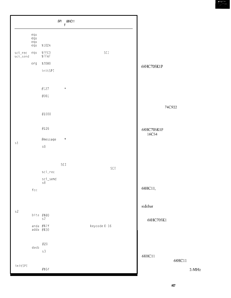
Listing l-Code to set up fhe on a
and make use of fhe LCD/keypad module is minimal. This
code was assembled using the freeware AS1 assembler.
DDRD
$1009
SPCR
$1028
SPSR
$1029
SPDR
* BUFFALO 3.4 monitor
routines
equ
start
jsr
ldaa
jsr
ldaa
Set KBDLCD module to COMMAND mode
jsr
SPItrans
ldaa
* Send an "LCD Clear" command
jsr
SPItrans
* Initialize the SPI port
11127
SPItrans
* This command is sent twice, as 1st
* byte received after power up may
* be misread
* LCD needs more time to process the
CLEAR command
* than for displaying chars to the LCD screen
ldx
al
dex
bne al
ldaa
* Set KBDLCD module to DATA mode
jsr
SPItrans
ldx
Point to the ASCIIZ message string
ldaa 0,x
beq
inx
jsr
SPItrans
* Send out string, 1 char at a time
bra sl
* LOOP: take a char from
in, send it to KBDLCD, and
* send the KBDLCD key pressed code back to host via
so
jsr
jsr
SPItrans
jsr
bra
message
'This is a test!'
fcb 0
* Send a byte in A out SPI, and return with rcvd SPI byte in A
SPItrans
staa SPDR
ldaa SPSR
beq
ldaa SPDR
* Take binary
*
and bias it into ASCII range
* Allow a short delay time for KBDLCD module
* to process the character to the LCD
ldab
s3
bne
rts
* Initialize the SPI at slowest rate: 62.5 kbps
ldaa
(continued)
l
The typical bus-cycle time of most
common microcontrollers is shorter
than that called for by the LCD
manufacturer. I have generally found
them to work, but there are no
guarantees.
I decided to make use of the SPI
port, which exists on most microcon-
trollers and is often unused. Using this
high-speed serial link and a Motorola
microcontroller, I have
designed a very simple LCD and
keypad interface which uses only the
three SPI signals from the host
controller. The serial port is also
handy if the operator’s panel is far
away from the microcontroller circuit
board itself.
The cost of the circuit is little
more than the
which it
replaces. I chose the Motorola micro-
controller since I’ve had their nifty $50
evaluation board and software for a
year or so now, and finally the
is available. I expect that
the
PIC family chips would also
serve my low-cost purpose, but I have
more experience programming the
Motorola family.
MAKING THE CONNECTION
For this circuit to be generally
useful, it must offer fast data transfers
to the LCD display and require very
little code support in the host
microcontroller. The Serial Peripheral
Interface (SPI) available on the
TMS370, and some of the
8031 derivatives, satisfies both these
criteria. If you are not familiar with
this functional block, refer to the SPI
for a brief overview of
Motorola’s implementation of it.
Readers familiar with the Motor-
ola
family are likely
saying, “Whoa-there is no SPI circuit
block in that chip”-which is correct,
of course. The trick used in this design
implements the SPI in software. I
wanted this circuit to work with SPI
ports on at least the two microcontrol-
lers that I commonly use-the
and the TMS370.
Of the two, the
is much
less programmable in terms of bit rate.
Its slowest SPI bit rate (with a
E clock) is 62.5 kbps or 16 us per bit.
Circuit Cellar INK
Issue April1995
37
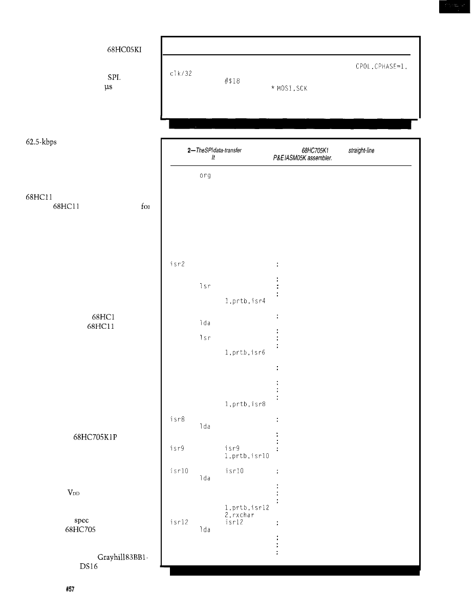
Getting that timing right is a critical
aspect of the code for the
(as I will cover fully later).
It takes 128 us to transfer a data
byte to the LCD over the
Since
the LCD needs about 50 between
each character it receives, this circuit
doesn’t slow things down too much.
Reasonably rapid LCD screen updates
are possible. As well, the keypad data
is returned to the host at the same
rate, although since the
keyboard-input functions are slow,
this is not a concern.
Code overhead on the host micro
is minimal. Listing 1 presents the
short routine for initializing the
SPI. It is important to note
that the
SPI block is set up
a clock phase and polarity of 1 since
this is the only way this circuit will
work! The code to send a message to
the LCD plus perform other functions
is also shown in Listing 1. Since the
BUSY signal of the LCD is not read by
the KBDLCD module, software loop
delays are built into the routines so
the KBDLCD module can keep up.
Although it is not shown in the
program code, it is very important to
remember to tie the
l’s -SS line
to Vcc to make the
the master
device. If you’re using a microcontrol-
ler without an SPI port, it would not
be too hard to write a bit-banging
routine to implement the SPI using
three I/O port lines. It would, how-
ever, have a slower data transfer rate
unless the processor was very fast.
THE HARDWARE
The entire circuit is detailed in
Figure 1. Apart from the crystal and its
capacitors, the
needs
nothing else other than 5 V to run. The
reset function is looked after internally
by the chip’s timer subsystem. How-
ever, this internal reset circuit releases
the processor from reset after 4064
clock cycles.
must be stable by
this time or correct operation will be
uncertain. If your power supply does
not come up to
quickly enough,
connect the
-RESET line to
the host -RESET line.
The 16-button keypad can be any
4
x
4 matrix such as a
001
or the DMC
membrane
38
Issue
April 1995
Circuit Cellar INK
Listing l-continued
staa SPCR
* Enable SPI as Master
ldaa
staa DDRD
made outputs
ldaa SPSR
* Clear flags
ldaa SPDR
rts
Listing
interrupt-service routine for
uses
code in fhe
interest of speed.. was assembled using fhe
RAM
rxchar
rmb
1
txchar
rmb
1
flag
rmb
1
org
ROM
* Mainline program code here
* SPI data transfer Interrupt Service Routine
IROISR
isrl
isr3
isr4
isr5
isr6
isr7
isrll
isr13
clr
rxchar
bil
isrl
bih
isr2
lda
txchar
sta
prtb
txchar
bil
isr3
brclr
bset
6,rxchar
bih
isr4
txchar
sta
prtb
txchar
bil
isr5
brclr
bset
5,rxchar
bih
isr6
Ida
txchar
sta
prtb
lsr
txchar
bil
isr7
brclr
bset
4,rxchar
bih
isr8
txchar
sta
prtb
lsr
txchar
bil
brclr
bset
3,rxchar
bih
txchar
sta
prtb
lsr
txchar
bil
isrll
brclr
bset
bih
txchar
sta
prtb
lsr
txchar
bil
isr13
; Ignore first MSB for lack of time
Wait until next falling edge
Send out bit 7
Shift for next time
Wait until rising edge
Wait for falling edge
Send out bit 6
Shift for next time
Wait until rising edge
Wait for falling edge
Send out bit 5
Shift for next time
Wait until rising edge
Wait for falling edge
Send out bit 4
Shift for next time
Wait until rising edge
Wait for falling edge
Send out bit 3
Shift for next time
Wait until rising edge
Wait for falling edge
Send out bit 2
Shift for next time
Wait until rising edge
(continued)
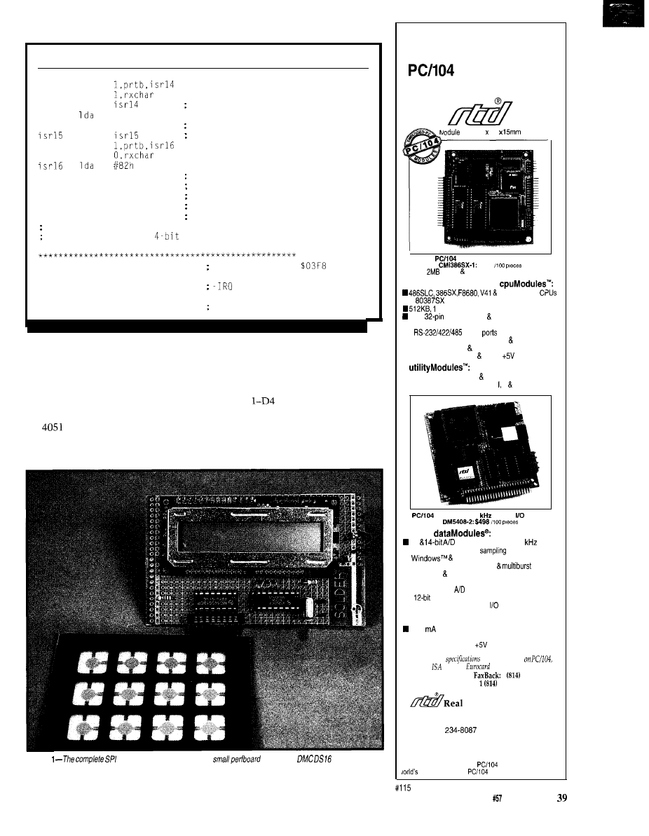
Listing P-continued
isr14
brclr
bset
bih
sta
bil
brclr
bset
sta
clr
txchar
Wait for falling edge
txchar
prtb
Send out bit 1
Wait until rising edge
ISCR
Clear IRQ flag since IRQ latch will
be set from 7 SPI clocks following
the initial one which caused this
ISR to be invoked
Zero out txchar
Additional code to send byte to the
LCD display, in two
nybbles
rti
org
vectors
Vectors begin at
dw
rom
dw
IRQISR
vector
dw
rom
dw
start
Reset vector
keypad that I used (see Photo 1). The
columns are scanned by sequentially
placing a high level on PAO-PA3. The
rows are sensed by sending four binary
combinations to PA4 and PA5, which
are connected to the address inputs of
the
multiplexer chip.
The chip then routes each row in
sequence to the PA7 port, configured
as
the sense input. The A port has
programmable pull-down circuitry for
any port bits configured as inputs, so
no additional resistor is needed.
Diodes D
prevent the possible
shorting of two PAO-PA4 data lines
should the operator hold two keys
pressed at one time. This would only
be a problem if the LCD was being
Photo
LCD/keypad circuit is built on a
and uses a
membrane
keypad.
REDUCE THE STACK!
Use fully integrated
CPU and DAS
modules from
size: 90 96
Compliant PC-AT SBC
$578
DRAM SSD software included
5 PC/XT/AT Single Board
VG230 DOS
n
math coprocessor socket on-board
MB, 2MB or 4MB DRAM installed
Two
SSD sockets support software
n IDE, floppy & CGA controllers
n
serial
n Bidirectional parallel, keyboard speaker ports
n Keypad scanning PCMCIA support
n Power management single
supply
7
n Super VGA controller I/O modules
n PCMCIA carriers for Types II Ill cards
Compliant 200
Analog
Module
17 DAS
12
conversion up to 200
n Gap free, high speed
under
DOS
n Programmable scan, burst
n Pre, post about triggers
n 1 K channel-gain scan memory with skip bit
n 1024 sample
buffer
n
analog outputs
n Bit programmable digital
with Advanced
Digital Interrupt modes
n Incremental encoder interfaces
4-20
current loop source
n opto-22 compatibility
n Low power & single
power supply
For
technical
and data skeets
bus and
products, call
RTD USA Technical
1
235-1260
RTD USA
BBS:
234-9427
Time Devices USA
200 Innovation Boulevard
l
P.O. Box 906
State College, PA 16804-0906 USA
Tel: 1 (814)
l
Fax: 1 (814) 234-5218
RTD Europa RTD Scandinavia
Fax:
(36) 1 212-0260
Fax: (356) 0 346-4539
RTD is a founder of the
Consortium and the
leading supplier of
CPU
and
DAS modules
Circuit Cellar INK Issue April 1995
updated at the same time, but it is a
possibility. The necessary
of
the switches is done in software.
The LCD module can be any one
of many inexpensive LCD modules
available on the surplus market that
use the Hitachi HD44780 LCD
controller driver. I am using the
Hitachi
a 16-character by
line module. With so few port lines
available on the
I had to
use the 4-bit transfer mode. From the
host micro’s standpoint, the LCD is
sent data as if it were an
device.
Port bits PAO-PA3 serve double
duty as the data bus for the LCD and
as the keypad-scan function described
earlier. Port PA4 also serves double
duty as the register-select signal for
the LCD and keypad column-multi-
plex address. PA6 is the LCD ENABLE
strobe signal. During the key scan,
ENABLE remains low so the LCD does
not receive extraneous data.
SPI data comes in to
and is
sent out on PBO. The SPI clock signal
is connected to the
input. Note
that the
line is pulled high by a
resistor. This ensures the
is not stuck in an ex-
tended interrupt prior to the host
micro’s proper initialization of the SPI
port pins. The power consumption of
the entire circuit, using a 16 x 2 LCD,
is 26.5
THE FIRMWARE
Steve Ciarcia has stated, “My
favorite programming language is
solder.” And, like him, I love building
circuits.
At times in the past, I have
happily wired complicated micropro-
cessor circuits, assuming that I could
write the necessary software later.
When I reach the software and firm-
ware stage, I am sometimes dashed by
the realization that I neglected to
investigate software considerations
such as critical timing.
In this case, I knew from the
outset that getting the
to
handle the SPI data transfers at 62.5
kbps was going to be tricky. I was also
concerned whether 496 bytes of
EPROM was going to be enough,
although I haven’t yet written an
assembly language program that was
42
Issue
April 1995
Circuit Cellar INK
Listing 3-The
LCD routines for the
LCD/keypad module are
for the
microcontroller.
*
display without
regs
*
LCD device. Invoke first.
*
char in A at current cursor position
temp
lcdwl
rmb
sta
bset
bclr
jsr
lda
sta
bset
bclr
jsr
sta
bset
bclr
jsr
sta
bset
bclr
jsr
jsr
jsr
jsr
jsr
rts
jsr
jsr
sta
bne
rts
jsr
jsr
rts
5 ms delay
sta
lcddl
bne
rts
prta
6,prta
6,prta
prta
6,prta
6,prta
prta
6,prta
6,prta
prta
6,prta
6,prta
lwritec
lwritec
lwritec
temp
lcdwl
temp
lwrited
temp
lcddl
temp
wait 50 for LCD to finish
= 4.6 ms
Listing
* write a byte to LCD command register
lwritec
sta
temp
lsra
lsra
lsra
lsra
sta
prta
RS line low
bset
6,prta
strobe ENABLE
bclr
6,prta
temp
sta
prta
bset
6,prta
strobe ENABLE
bclr
6,prta
rts
* write a byte to LCD data register
lwrited
sta temp
lsra
lsra
lsra
lsra
RS line high
sta
prta
bset
6,prta
strobe ENABLE
bclr
6,prta
temp
RS line high
sta
prta
bset
6,prta
strobe ENABLE
bclr
6,prta
rts
too big for the EPROM space I had
some housekeeping, then enters a
available.
polling loop to wait for the next SPI
Therefore, I first designed the
clock. The first
data bit (MSB) is
transfer part of the program, calculated
its timing, and when satisfied it would
work, built the circuit. I am hoping
that some of this methodology rubs off
onto future projects!
Listing 2 shows the SPI interrupt
service routine. The SPI data handling
is performed using a pseudointerrupt
technique. That is, the SPI clock (from
the host micro), connected to the
line, generates an interrupt for the first
clock (of an SPI transfer) received. This
interrupt is necessary to ensure that
the
is always ready to
receive a byte of SPI data.
However, the interrupt latency is
10 cycles plus the time it takes to
finish the instruction being executed.
This is too long a period for the
to send and receive a bit.
The trick is to settle for 7-bit
transfers, which are suitable for the
LCD. The keypad-data output needs
only 4 bits. The first SPI clock invokes
the interrupt-service routine, does
simply ignored. The
has B I H
and
B I L
instructions for tightly polling
the IRQ pin level. Using these instruc-
tions and tight, replicated,
code,
the program can both send and receive
the SPI data with no problems.
Since SPI data is sent MSB first,
the transmitted byte (keypad data)
must be bit reversed before being sent.
There is plenty of time to do this bit
reversal during the keyboard-scan
routine using a 16-entry lookup table.
I should note that it is critical that
the IRQ flag-clearing instruction be
included at the end of the ISR. During
the execution of this ISR, seven
additional falling clock edges have
been applied to the
line, and its
latch will definitely be set. Without
the flag-clearing instruction, the ISR
would be reentered even though the
SPI data byte has been fully sent and
received.
The circuit returns values of 1-16
to the host for the 16 different keys. A
American Eagle Technology
Data acquisition rates from
to 1 MHz.
Newest designs incorporate
the latest technology: FIFO
buffers, dual-DMA, REP INSW
data transfers, programma-
ble gains, etc.
Simultaneous sampling
option for all boards.
Lowest prices on the market
for comparable performance.
Digital I/O
on-board relays.
16-bit analog output (D/A).
Large inventory of popular
items for next day delivery.
Also available: signal condi-
tioning, multi-port serial
boards, device programmers,
logic analyzers, much more.
A m e r i c a n
Eagle Technology
526 Durham Rd
Madison, CT 06443
Call: (203) 245-6133
Fax: (203) 245-6233
Circuit Cellar
INK issue
April1995
4 3
value of zero is sent when no keys
Cursor mode
next byte(s)
have been pressed since the last
sent move the cursor to the re-
inquiry from the host.
quested position
Remember that the
ASCII set can be transmitted to the
LCD using seven bits. To send data to
the command register for such opera-
tions as display clearing, I have
“stolen” three seldom-used character
values (125-127) for that purpose. The
definitions of these three commands
are as follows:
Data mode 126 J-the next
s) sent
go to the data register of the LCD
Command mode
next
byte(s) sent go to the command
register of the LCD
All necessary commands to the
LCD are seven bits long with the
exception of the cursor-movement
command, which has an additional
mode assigned to it. All values passed
to the LCD while in this mode have
DB7 set high as required for cursor
movement.
The necessary code (with atten-
dant timing constraints) to set up the
LCD display properly in 4-bit mode
executes when the
is
powered up. The host micro need not
worry about this other than to wait
ms or so after reset before sending any
Serial Peripheral Interface
The Serial Peripheral Interface (SPI) is a high-speed,
The CLOCK signal needs further explanation. The
TTL-compatible, full-duplex, synchronous, data-transfer
rate of data transfer depends on the CLOCK rate. In the
protocol. It has been implemented as a functional block
the clock rate is based on the processor clock
on many modern microcontrollers including the
divided by the constants 2, 4, 16, or 32. The standard
TMS370, and some derivatives of the 8051
processor clock rate for the
is 2 MHz. This
family. While they’re not all that common, there are
project uses the
option, as the
in the
peripheral
designed for this serial bus.
keyboard and LCD module cannot respond to higher
For instance, Maxim and Linear Technology make
rates. This selection provides a transfer rate of 62.5 kbps.
multichannel 12-bit
Texas Instruments makes
Incidentally, the TMS370 provides a much more
and power driver
(these make excellent
grammable SPI clock-rate selection with a divisor ratio
stepper motor drivers). Motorola’s LCD driver
use a
of up to 1024 on its internal clock.
serial interface, which can be driven by the SPI. These
The
block offers both the clock polarity
are just a few examples of available devices.
and phase to be programmed. Through this, the SPI
The
functional block, which I outline, is
works with peripheral
made by many manufacturers.
implemented by Motorola in their
family.
Due to the way in which the
firmware
There are slight differences in the implementation of
works, it is important that both the clock phase and
this protocol in other manufacturers’ products, but the
polarity be set to 1 for this project.
principle is the same.
The SPI is a full-duplex protocol
Data transfer is serial and, unlike the more
Unlike other common, full-duplex protocols such
mon RS-232 standard, is synchronous. Since this bus
as the RS-232 where there is not necessarily a 1: 1
was originally intended to provide communication
relationship between the amount of data sent and that
among microcontrollers in a multiprocessor
received, the SPI does impose this constraint. For every
ment, the concept of a master and slave is used.
byte sent out by the master, a byte is simultaneously
In environments, where both devices on the bus are
clocked in to the master. Whether the slave actually
“intelligent” and therefore capable of originating
sends back data is immaterial. The master assembles a
messages on their own, the protocol allows only
one
of
byte of data from the signal seen on its
line during
the devices to be the master. So, only the master can
the time its data byte is being sent out.
initiate messages; the slave receives and responds to
For the purpose of sending data from the master to
these messages. In a project such as this one, the host
an output-only peripheral such as a DAC, this incoming
microcontroller must be programmed as the master; the
byte would be ignored. In the case of an SPI device such
keyboard and LCD module is the slave. (Program code
as an ADC, which must be triggered and then read, the
and implementation are detailed in the article.)
common method is for the ADC to return the last
The SPI uses three signals to transfer the data:
reading it took at the time that it is receiving its trigger
MOSI (Master Out Slave In),
(Master In Slave
command for the new conversion. ln this project, the
Out), and CLOCK. Since the
is the host or
module returns the last key pressed whenever it receives
Master processor, the MOSI line carries data to the LCD
an incoming LCD data byte.
and the
carries data from the keypad to the host
The
SPI block, while very flexible, has a
[they would be reversed if the
were the slave).
fixed
word length. The TMS370 SPI block has a
The i
n i t S P I
procedure in Listing 1 gives the
fully programmable word length of
bits. While the
correct sequence of
instructions for setting the
SPI is certainly not as flexible as the
bus, it is much
SPI properly. Note also that the
line of the
easier to use when only a small number of devices need
must be tied to V
CC
to enable it as the master.
to be connected together.
44
Issue
April 1995
Circuit Cellar INK
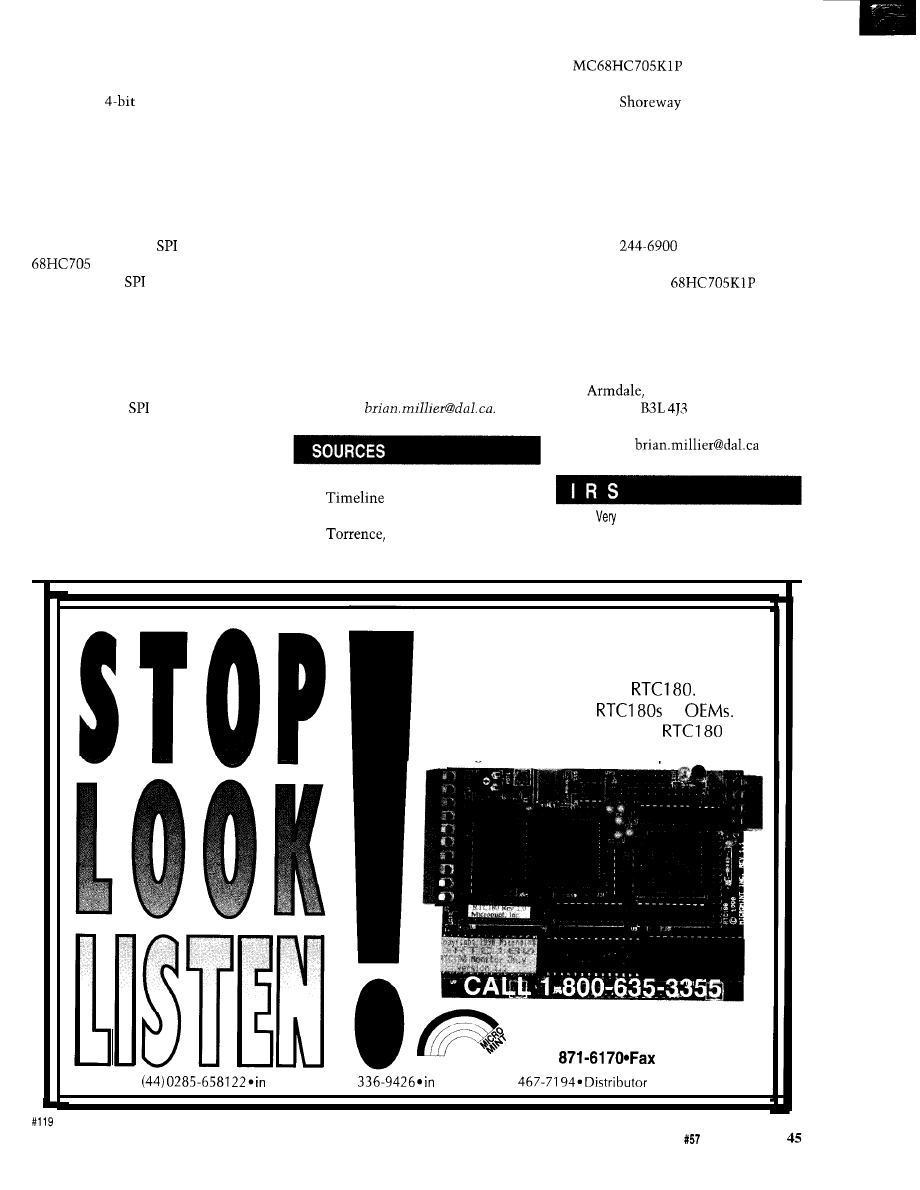
data to the LCD and keypad circuit.
For those who want to use these LCD
modules in
mode in their own
applications, I have shown the re-
quired code in Listing 3. The Hitachi
HC44780 data manual is a comprehen-
sive source of information on program-
ming these modules.
So the builder can see if the circuit
is working properly prior to being
connected to a host
port, the
sends out the sign-on
message “CIC
LCDKBD” after it
initializes the LCD module. Once
connected to a host, the first LCD
command should be to clear the LCD
of the sign-on message.
To read the keypad, the host sends
a byte to the SPI. The key code is
returned in the
data register with a
zero indicating no key presses since
the last poll. If you want to read the
keypad without also writing to the
LCD, send code 126, which sets up
data mode (the mode most commonly
used). Note that this circuit “remem-
bers” the last key pressed since the
last host polling. This feature ensures
that if critical timing sequences are
performed, the host is able to check
the keypad less frequently.
WRAP-UP
I hope this article prompts anyone
who hasn’t bothered to make use of
the SPI to give this simple, yet useful,
circuit a try. It can be breadboarded in
about an hour or so.
q
Brian Millier has worked as an
instrumentation engineer for the last
12 years in the Chemistry Department
of Dalhousie University, Halifax, NS,
Canada. In his leisure time, he
operates Computer Interface Consult-
ants and has a full electronic music
studio in his basement. He may be
reached at
LCD module
Inc.
23650 Telo Ave.
CA 90505
(3 10) 7845488
Jameco Ltd.
1355
Rd.
Belmont, CA 94002-4100
(415) 592-8097
Motorola Technical Manuals
Motorola Literature Distribution
P.O. Box 20912
Phoenix, AZ 85036.
(602)
A programmed
is
available for $15 plus $3 postage
and handling (U.S. currency) from:
Brian Millier
Computer Interface Consulting
P.O. Box 65, Site 17, R.R. 3
NS
Canada
(902) 876-8645
E-mail:
410
Useful
411 Moderately Useful
412 Not Useful
Odds are that some time during the day you
will stop for a traffic signal, look at a message
display or listen to a recorded announcement
controlled by a Micromint
We’ve
shipped thousands of
to
Check out why they chose the
by
calling us for a data sheet and price list now.
MICROMINT, INC.
4 Park Street, Vernon, CT 06066
(203)
(203) 872-2204
in Europe:
Canada: (514)
Australia: (3)
Inquiries
Welcome
Circuit Cellar INK
Issue
April 1995
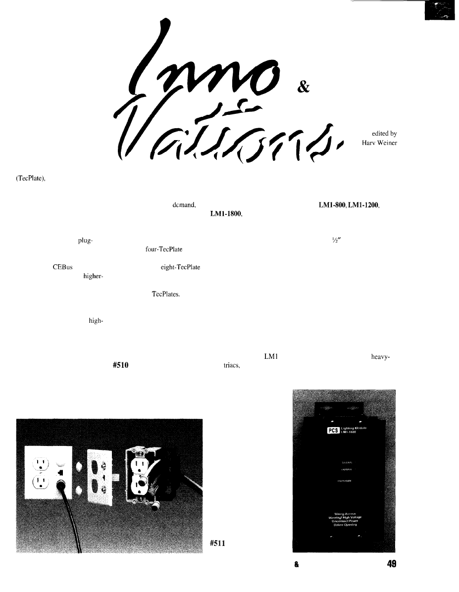
PLUG-IN FREEDOM
FOR THE DIGITAL
HOME
An affordable, home-wiring
system that fulfills consumers’
immediate demands for home
networking of computers,
security systems, and other
electronic products also offers a
convenient on and off ramp to
the coming information
superhighway.
The new
TecSystem
from
U.S.Tec is the backbone to an
easy-to-use home LAN.
Consisting of a wall plate
a central electronic
server, and special networked
cabling, the TecSystem allows
homeowners to access cable TV,
telephone, and electricity from a
single, convenient wall source.
Installed in multiple locations,
the TecSystem enables
and-play flexibility with other
electronic devices in the home.
TecSystem is
compliant.
The system’s use of
bandwidth-capacity wiring
prepares homeowners both for
in-home automation of elec-
tronic products and appliances,
and two-way access on the
speed, high-volume digital
superhighways. The TecSystem
allows you to view VCR and
security camera pictures on
multiple TVs, network comput-
ers to printers, and send stereo
audio from room to room. Home
LAN is well-positioned for
problem-free communication
with global computing networks,
programmable news and
information, video on
multiple TV channels, and other
multimedia services.
TecSystem comes in
multiple configurations. An
entry-level,
network can be installed for as
little as $500. An
network is priced at
$1500.
A
complete network accommo-
dates up to 32
U.S.Tec
470 South Pearl St.
Canandaigua, NY 14424
(716) 396-9680
Fax: (716) 394-7095
IN HOME
AUTOMATION
BUILDING
CONTROL
HIGH-POWER, PERMANENTLY WIRED
X-10 LIGHTING MODULE
The PCS lighting control modules,
and
finally offer an economical solution to controlling more
than 500 W of incandescent lighting using X- 10 signalling. These
modules are mounted on a flat, vertical surface and are permanently
attached to the residence wiring system. Two
knockouts and a
terminal block are provided for simple connection.
All controllers offer the same advanced features available on all
PCS multimodules. These features are not available on any conven-
tional lighting modules.
Lights can be brightened from full off without having to come
to full on first. They also can dim down from full on. If dimmed past
the lowest dim level, the module enters the full-off state, allowing it
to go to full on with the next on command.
Another feature is that the current dim level is not lost if the
module is turned off or if power fails. Each time the module receives
an on command, it returns to the preset dim level, allowing the user
to preset various indoor and outdoor lighting levels.
All versions of
are thoroughly overdesigned with
duty
more than adequate heat sinking, EM1 protection, and all-
metal enclosures. Modules are in the process of being UL listed.
All lighting modules
can be optionally turned on
and off by an external
switch in series with the
load, typically a standard
wall switch. This is a
convenient method of
providing external manual
control to every lighting
circuit.
Powerline
Control Systems
9031 Rathburn Ave.
Northridge, CA 91325
(818) 701-9831
Fax: (818) 701-1506
HOME AUTOMATION BUILDING CONTROL APRIL 1885
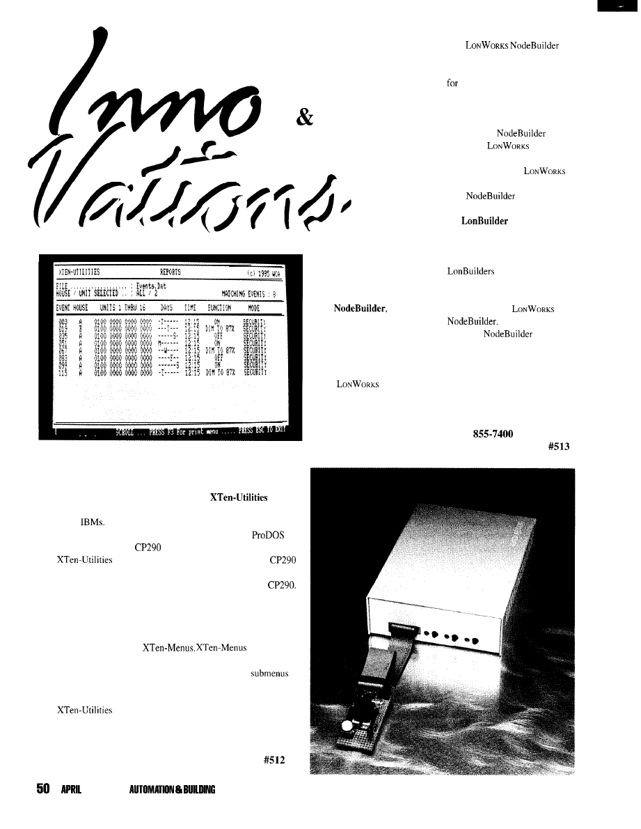
IN HOME
AUTOMATION
BUILDING
CONTROL
X-10 SOFTWARE FOR THE REST OF US
Wilmington Computer Applications has released a simple,
nongraphics, menu-driven X-10 software package for use on most
IBM PC, XT, or AT and Apple II computers.
requires
only one floppy, a serial port, 256 KB memory, and MS-DOS 2.0 (or
newer) for
The Apple II version requires one floppy, super
serial card (or equivalent), 64 KB memory, and includes
8.
Both versions require the
X-10 home control interface.
offers file-based editing and reporting. A
does not have to be connected while editing an event file or produc-
ing reports. Modified event files can later be uploaded to the
The Reports command details house and unit usage. A countdown
Timer function allows delayed X-10 device control. An adjustable
Oscillate function can be used to cycle X- 10 controlled devices,
including Power Horns, on and off.
Both versions include
allows easy
two-keystroke control of any X-10 device and is easy to set up. You
can even use your own descriptions on menus. Up to 16
can be selected from the main menu. Any menu item can turn any
one house code or multiple-unit combination on, off, dim, or flash.
is priced at $39.95.
Wilmington Computer Applications
P.O. Box 429
l
Wilmington, MA 01887-0429
(SOS) 658-9950
LOW-COST TOOL
FOR DEVELOPING
INTELLIGENT DEVICES
Echelon Corporation intro-
duces
a new
development tool that makes it
easy and inexpensive for manu-
facturers to design devices that
can be integrated into automa-
tion and control networks. In-
stalled
nodes today
range from valves in chemical
plants, to alarms in telephone
central offices, to sensors for
automated toll booths, to smart
thermostats for homes.
includes everything developers
need to create and test products
LONWORKS-based control
networks. It uses a familiar
Windows-based development
environment with easy-to-use,
on-line help.
in-
cludes the
Wizard, a
tool which generates software
for an interoperable
device.
complements
the development capabilities of
the
Developers
Workbench, a tool with sys-
tems-level capabilities. System
developers can use one or more
for network devel-
opment while simultaneously
developing individual nodes for
the system using
The
is avail-
able for $3,995. For more infor-
mation on LonBuilder Develop-
ers Workbench, call Echelon.
Echelon Corporation
4015 Miranda Ave.
Palo Alto, CA 94304
(415)
Fax: (415) 856-6153
1995 HOME
CONTROL
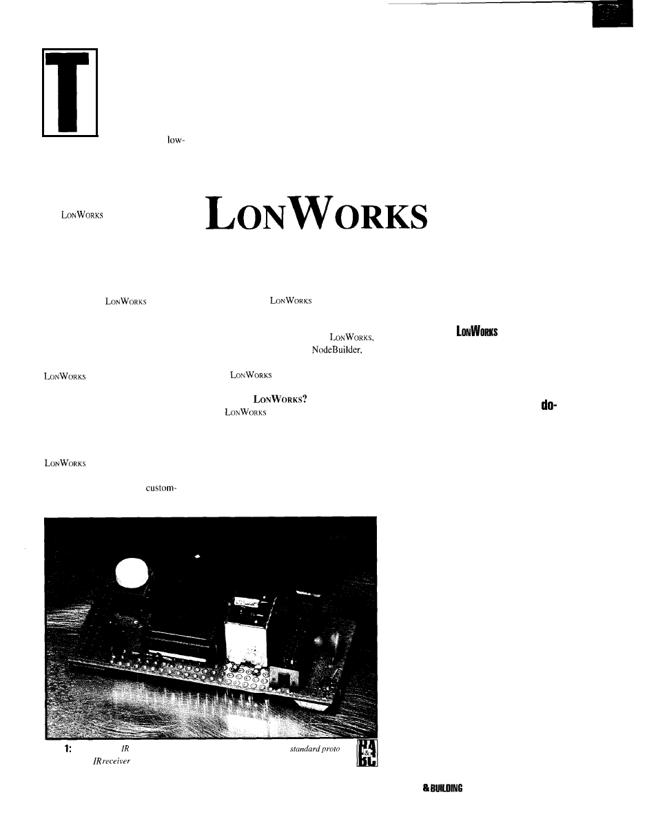
1
oday, the market for
home automation
seems to be divided
between whole-
house automation
systems costing
tens of thousands of
dollars and the
cost, do-it-yourself market. What’s
missing is a systems-level approach
providing the features of a whole-
home system that is simple to install,
is reliable, and comes at a low-cost.
technology is
Echelon’s answer for that gap. It
provides a method of communicating
between devices using several types
of media primarily for control.
Although initially used mostly in
industrial and commercial building
control settings.
has
become sufficiently popular that its
prices have been driven down. It is
now positioned for the low-cost home
automation market.
Special codes embedded in each
device (e.g., a heater,
thermostat, home theater center) are
transmitted via the home’s power
lines (the technology is also available
for twisted-pair, RF, infrared, coax,
and fiber-optic media). To meet the
desire for plug-and-play products.
provides a basic configu-
ration which requires no installation
or programming. For more
Developing Home
Automation
Devices with
ized automation,
devices can be
programmed or integrated with other
professional control systems.
After a brief introduction of
this article will focus on the
a
development tool which enables engineers to
create
devices.
WHAT IS
technology is a system of
sensors, actuators, displays, and logging
devices (referred to as nodes) linked together
to monitor and control electrical devices.
Control functions are typically handled
automatically, except for faults which the
system cannot correct. In home automation
RICH BLOMSETH
Rich believes
technology
fills the gap between whole-house
automation systems costing tens
of thousands and the low-cost,
it-yourself market. It provides a
common device control scheme
and communicates over media
often already installed in the home.
Photo
The prototype
dimmer hardware was easily constructed using
board and an
from
Radio Shack.
HOME AUTOMATION
CONTROL APRIL 1995
5 1
applications, a control network may provide
safety (e.g., monitoring security, fire alarms,
and pool and spa areas), control (e.g., reg-
ulating room temperature, lighting, draper-
ies, and irrigation systems), and entertain-
ment (e.g., managing
equipment).
Neuron chips, the heart of
technology, contain the protocol
that enables them to communicate with other
Neuron chips. Since Neuron chips can be
connected directly to the sensors and outputs
they supervise, a single Neuron chip handles
processing of sensor and output status,
execution of control programs, and commu-
nications with other Neuron chips.
For nodes requiring more processing or
power, the Neuron chip can also be used
as a communications coprocessor for any
other processor. The Neuron chip therefore
provides a scalable solution that can be used
even on complex nodes which include a host
computer and network interface.
also provides
ability with other control systems. Network
management software, tools for installing
complex networks, and routers enable
communications between the different
communications media.
RIDING THE POWER LINES
Power-line signaling is ideal for
automation communications because it
requires no new wires. As well, power
wiring already reaches every device that
needs to be controlled.
Although power-line signaling devices
have been available for years, they have two
significant drawbacks-they are unreliable
and lack two-way communication. Intermit-
tent noise sources, impedance changes, and
attenuation conspire to make the power line
a hostile path for power-line signaling.
To counteract these problems,
W
ORKS
combines narrowband signaling with
signal processing and error correction
algorithms in its transceivers. The trans-
ceiver features include:
l
low-overhead error correction to enable the
system to receive corrupted packets while
maintaining a high throughput
l
adaptive carrier-detect algorithm that
automatically tracks changes in
line noise levels
l
impulse-rejection technology to improve
performance in the presence of impulsive
noise sources such as triac-controlled
dimmers
By declaring
objects and network variables for an IR dimmer,
any
device
on the same network con communicate with the dimmer.
I R D i m m e r C o n t r o l l e r ”
n e t w o r k o u t p u t
n e t w o r k o u t p u t
Device Name and Direction
Bit, nybble, byte input and output
input and output
Dual slope input
Edgedivide output
input
Frequency output
input and output
Infrared input
Leveldetect input
Magcard and Magtrackl input
Muxbus input and output
Neurowire input and output
Pulsecount output
Pulsewidth output
output
and Period input
Parallel input and output
Pulsecount and Totalcount input
Quadrature input
Serial input and output
Touch input and output
output
Triggeredcount output
Wiegand input
Direct binary
Up to 16 bits of clocked serial data
Comparitor input for 16-bit dual-slope
Waveform equal to fraction of input
Edge to edge timing of an input stream
Square wave output of specified frequency
Philips K-compatible serial I/O
Encoded input from an demodulator
Detect logic zero level
IS0781 1 track 1 and 2 magnetic card readers
Multiplexed address and data bus
SPI and Microwire compatible serial
Output specified number of pulses
Output specified frequency and duty cycle
Single output pulse of specified period
Pulsewidth and period measurement
8-bit bidirectional
Transition count over fixed or total interval
Shaft encoder rotary position input
8-bit asynchronous serial
Dallas Touch 1 -wire bus
Pulse delayed with respect to input edge
Pulse controlled by counting input edges
Wiegand card reader input
Table 1:
Built-in Neuron C I/O objects
interfaces to most common I/O devices.
dimmer software declarations for I/O objects configure the Neuron chip’s
internal hardware for the IR dimmer I/O devices.
o u t p u t b i t
=
i n p u t q u a d r a t u r e
i n p u t i n f r a r e d i n v e r t
i n p u t b i t
i n p u t 1 e v e l d e t e c t
The complete IR dimmer software listing shows how little code is requiredfor a
complex application.
I R D I M M E R . N C - D i m m e r c o n t r o l l e r w i t h m a n u a l a n d
i n p u t s . C o m p a t i b l e w i t h t h e S o n y
r e m o t e
T h i s r e m o t e p u t s o u t t h r e e
i d e n t i c a l c o d e s
c l o s u r e .
n f r a r e d
c o n t r o l .
f o r e a c h k e y
= 2 . 6 m s ; l o w b i t = 1 . 1 m s ; h i g h b i t . = 1 . 9 m s
O b j e c t I D
0 0
S w i t c h s e n s o r o b j e c t ,
i i p r a g m a
I R D i m m e r C o n t r o l l e r ”
iipragma enabl
ups
i i p r a g m a
3
continued
APRIL 1995 HOME AUTOMATION
CONTROL
listing 8:
Open-Loop Sensor
Object, ID
network output
network output
network input
output bit
= 1;
input quadrature
input infrared invert
input bit
input leveldetect
IR controller values
#define
149
#define
146
#define
147
the state of the switch output.
void
nvoSwitch.state = !nvoSwitch.state;
nvoSwitch.state 0
the switch level by a specified
amount. Turn on the switch if the new level is not zero
and the switch is off.
void ChangeSwitchLevel(long int
long int
switch temporary update value
= nvoSwitch.value +
*
nvoSwitch.value = (unsigned)
?
0
?
if
ToggleSwitchStateO;
Infrared data input task-Read data from infrared remote.
priority
to
unsigned int
IR data
if
= (unsigned
switch
case
ToggleSwitchStateO;
break;
case
break:
case
break;
65424UL +
==
On/off control.
Invert
state of switch and
control LED.
Volume up control.
Increase brightness.
Volume down control.
Decrease brightness.
Ignore the other two outputs
Quadrature dial input task-Read data from shaft encoder.
Push button input task-Read data from on/off push button.
to
Add a
voice
to your system.
of up to 255 words or phrases (2 min total
your own using our
SDS-1000
development system
and
compatible,
prerecord your messages for you. Eprom voice storage
means your
IS
unaffected by power loss.
l
Repeater identifiers
l
ATM’s
l
Site alarms
l
Multiple languages
l
Emergency
l
Remote telemetry
announcements
Several different models
Palomar Telecom, Inc.
1201 Simpson Way
CA 92029
619-746-7996
619-746-1610
Complete line in stock
TW523 kit (DOS)
TW523 kit (Windows)
WI
Group Inc.
Voice: (905) 946-2451
l
Fax: (905) 479-0455
BBS: (905) 479-0469
Home
Automation
Worthington
Distribution
NO
HANDLING FEES
TRUE
Gumbletown Road, Paupack, PA
APRIL
1995
53
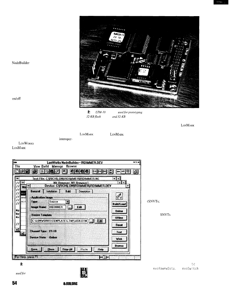
Since the technology complies with
signaling regulations in North America and
Europe, developers are able to expand their
potential market significantly.
DEVELOPING AN
INTEROPERABLE IR DIMMER
To give you an idea of how to take
advantage of this technology, I will work
through a simple example. You will see how
can be used to develop an
interoperable, remote-controlled dimmer for
the home.
The IR dimmer is a wall-mount dimmer
controller with a quadrature dial and push
button for manual input. An infrared receiver
offers input from a hand-held remote
controller. A single LED output is used as an
indicator.
FIRST THE SOFTWARE
Applications for the Neuron chip are
written in the Neuron C programming
language. Neuron C is based on ANSI C,
with extensions for network communica-
tions, I/O, and event-driven task manage-
ment.
Network communications for
able
devices are performed using
objects. These objects define
standard formats and semantics for how
Photo
The
module is
andproduction. It includes a Neuron 3150
chip,
memory,
RAM.
information is exchanged between devices
on a network. The most common objects are
sensors and
actuators.
A sensor object corresponds to a physical
device which can be monitored, whereas an
actuator object corresponds to a physical
device which can be controlled. For the IR
E d i t
O p t i o n s
W i n d o w H e l p
Photo
This device definition specifies the
application code and hardware device template to
be
the IR dimmer.
APRIL 1885 HOME AUTOMATION
CONTROL
dimmer, there is a single
sensor object.
Each object is defined by a
unique object type number and a
defined collection of network
variables. To a Neuron C application,
each network variable looks like a
standard C variable. Unlike the
standard C variable, however,
network variables can be connected
between devices. Therefore, updates
to a network variable on one device
automatically update the connected
network variables on other devices,
Network variables have types
like C variables, but a predefined set
of Standard Network Variable Types
pronounced “snivits”) go
beyond C types by also defining
standard units and ranges. For
example,
are defined for
temperature, pressure, and velocity.
Another difference from standard
C variables is that network variables
have a direction. Output network
variables automatically send their
values to other devices when updated.
Input network variables are automati-
cally updated when they receive
updates from other devices.
For the IR dimmer, there are two
output network variables: n v o Sw i
h
and
The
output reports the on/off state and
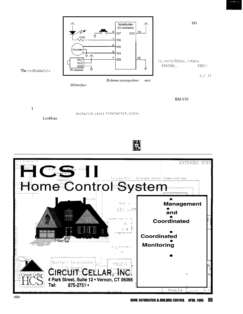
level of the dimmer. This
output can be connected to
network lamp modules which
control their level. However,
the output can be connected to
other devices as well. For
example, by connecting a
networked amplifier device,
you could control the on/off
state and volume of the
amplifier output.
output reports valid infrared
commands and could imple-
ment other types of IR control.
You could connect this output
to a central controller to invoke
GND
control applications for the home
new value to the IR dimmer sensor output
network.
value:
Listing contains Neuron C
statements which specify that the IR
dimmer has a single
sensor
(object type 1) and declares the two
network variable outputs.
Once declared, output network
variables are updated with a simple C
assignment statement. For example,
the following C statement assigns a
Interfacing to I/O devices is as simple
as network variables. Table 1 lists the 33
built-in device types that Neuron C includes.
These types provide built-in support
for the most commonly used I/O
devices in home control.
figure 1: The schematic for the
how
of the
is implemented internally in the Neuron chip.
Interfacing to any of these types
is done by declaring an
object
and then reading or writing it with a
function call. For example, Listing 2
declares the five I/O objects for the
IR dimmer.
The following statement reads
the IR sensor:
12,
65424UL +
The input parameters to the i
n
call define the number of bits (i.e.,
12) per command and the threshold
period to distinguish between the one
and zero input. These parameters are
selected for a Sony
remote control.
Other remote controls can be used by
changing the timing parameters. For this
project, all testing was done with a Sony
remote control and a Sony-compatible
universal remote control.
Processing for network variables and
I/O objects is accomplished within tasks.
Neuron C tasks are independently scheduled
statement sequences. Each task is defined by
one or more when statements that specify the
Energy
S e c u r i t y
A l a r m
Home Theater
Lighting
and Data
Collection
Get all these capabilities and
more with the Circuit Cellar
HCS II. Call, write, or FAX us
for a brochure. Available as-
sembled or as a kit.
(203)
Fax: (203) 872-2204
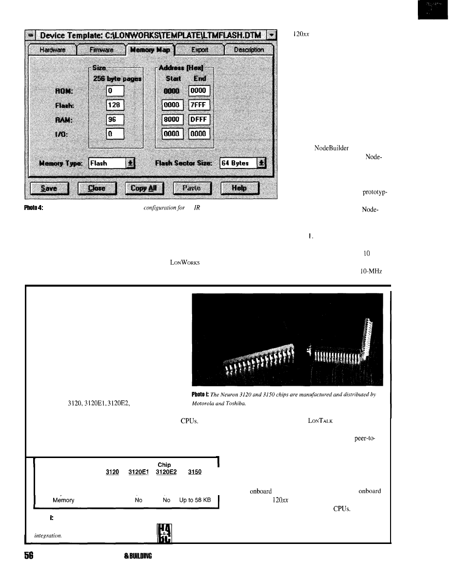
This device template defines the hardware
the
dimmer.
events that must be true before the task can
be scheduled.
The complete code for the IR dimmer is
quadrature input dial is moved, and one that
executes when
the on/off button is pressed.
shown in Listing 3. There are three tasks:
DESIGNING THE HARDWARE
one
that executes when an IR input is
applications can be
received, one that executes when the
designed around any of the three Neuron
3
chips (for description of the
chips, see the Neuron Chip sidebar),
the Neuron 3 150 chip with 2 KB of
on-chip RAM and up to 58 KB of
external memory, or any other
microcontroller as long as the Neuron
chip is used as a communications
coprocessor. Because of the extensive
support provided by the Neuron chip
firmware, the IR dimmer application
requires only 486 bytes of memory
and easily fits in a Neuron 3 120 chip.
The IR dimmer was prototyped
using the
hardware. The
LTM-10 node included with
Builder provides a complete prototype
node. The infrared decoder, quadra-
ture dial, input button, and output
LED were constructed on a
ing board
shown
in Photo 1. This
board was plugged into the
Builder hardware. The schematic for
the prototype I/O board is shown in
Figure
Prototypes may also be easily
constructed using the LTM- module
(see Photo 2). The LTM-10 module
includes a Neuron 3 1.50, a
The Neuron Chip
The Neuron chip (see Photo I) uses advanced
CMOS VLSI technology to implement low-cost control
networks. Included in each Neuron chip are all the
functions required to acquire and process information,
make decisions, generate outputs, and propagate control
information via a standard protocol. Communication
takes place across a wide variety of network media such
as twisted-pair cable, power line, infrared, radio
frequency, or coaxial cable.
Neuron chips are manufactured and distributed by
Motorola and Toshiba. They are available in four
versions: the
and 3150 chips.
All versions are highly integrated, require a minimal
number of external components, and include three 8-bit
One CPU executes user applications, which could include
measuring input parameters, timing events, making logical
decisions. and driving outputs.
Neuron
The second CPU executes the
protocol.
Messages are properly encoded and decoded for distribution
over the network. This protocol supports distributed,
peer communication that enables individual nodes, such as
actuators and sensors, to communicate directly with one
another.
EEPROM bytes
RAM bytes
ROM bvtes
The third CPU controls the Network Communication
512
1024
2048
512
1024
1024
2048
2048
Port, which physically and packets.
sends receives the
10.240
10.240
10.240
0
I
There is
EEPROM and RAM, and either
Ext.
Interface
No
Table Neuron chip memory configurations
provide a range of options
for memory
size and
ROM (Neuron 3
chip) or an external memory port
(Neuron 3 150 chip) to support the three
Table I summarizes the memory configurations of
the four Neuron chips.
APRIL 1885 HOME AUTOMATION
CONTROL
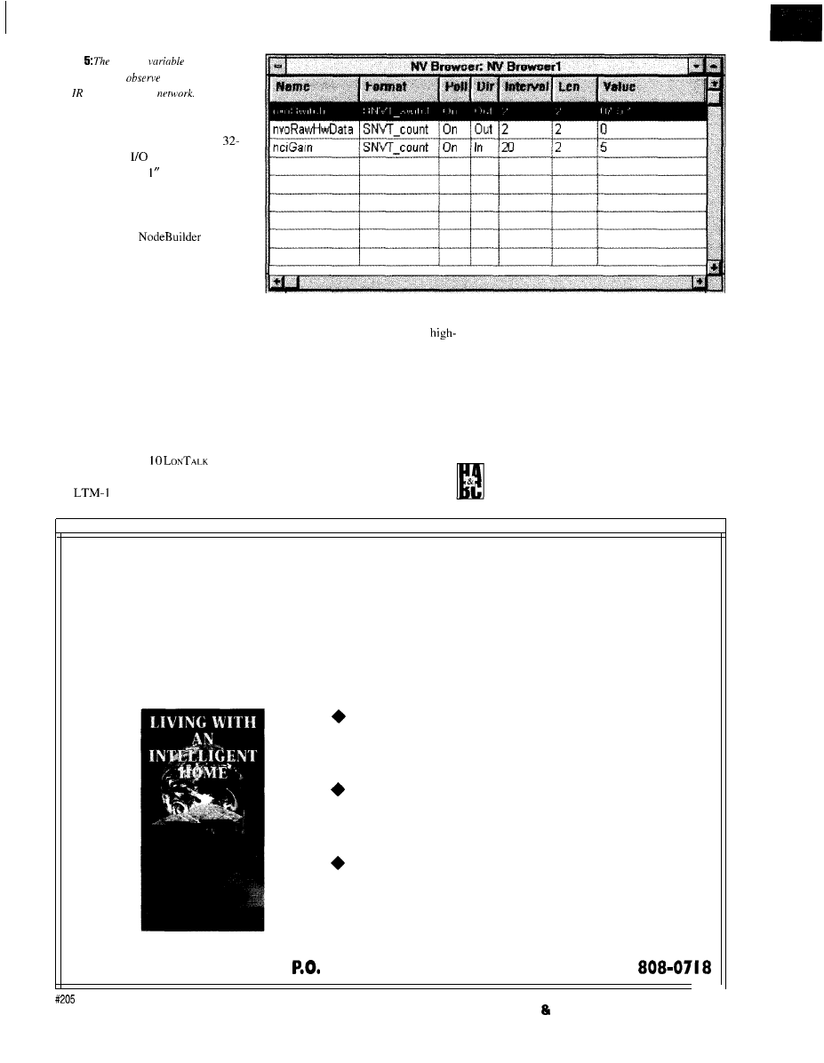
Photo
network
browser
makes it easy to
and manipulate
the
dimmer over the
crystal, 32-KB flash memory, and
KB RAM. The
and communica-
tions pins are all 0. centers for easy
prototyping.
DEFINING THE DEVICE
A device in
is
defined using a device file. The
device file defines the device’s
hardware characteristics and specifies
which Neuron C application the
device needs. The
screen
shot in
Photo 3 shows the device definition
for the IR dimmer.
The IR dimmer device is defined
by specifying the application program
tobethe
IRDIMMER.NCfiledescribed
earlier. For prototyping, the device
template is defined to as
LTMFLASH
to
specify that the hardware will be
based on the LTM-
module with the application stored in
the
0 flash memory.
When the device is ready for
volume production, the device template can
be changed to the 3 120 template. The default
device templates simplify hardware
definition, but a custom template can be
defined for any hardware configuration. The
device template is easily modified by
clicking on the Edit button next to
the template name. Photo 4 shows
the memory tab of the device
template for the LTM-IO module.
PROGRAMMING THE DEVICE
With the Neuron C application written
and the IR dimmer device defined, you are
ready to compile the program and program
the device. You do this by simply clicking
the Build/Load button in the Device window
shown in Photo 3. This automatically installs
the device hardware, invokes the compiler
and linker with the parameters specified in
the device file, downloads the new applica-
tion to the device, and starts the new
Let’s Work Together.
Networking provides access to a world of resources, and Home
Systems Network offers a world of resources to those who are
interested in home automation. Check it out.
Are you looking for information?
Obtain unbiased information about how to install and
use all types of home automation systems from our
books and Intelligent Home video tape series.
Are you looking to identify sources?
Call our toll free number for a list of sources for any
type of home automation dealers, products, or
services.
Are you looking for marketing assistance?
List your products and services in the Home Systems
Network database and let us tell the world about them
through our books, video tapes, television shows and
referral services.
HOME SYSTEMS NETWORK
BOX 3006
EDMOND, OK 73083
(800)
HOME AUTOMATION BUILDING CONTROL APRIL 1995
57
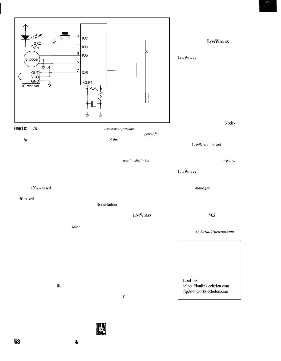
Neuron chip
Low-voltage,
link-power,
twisted-pair network
104
Link Power
X
CPO-2
Transceiver
LPT-10
X
CLK2
X
The
dimmer device with a link-power twisted-pair
the simplest implemen-
tation since no local power supply is required. The LPT-10 transceiver supplies sufficient
the
entire dimmer device. Other transceivers can be used in place
LPT-10 to communicate on other
media without having to change the core of the design
application. The downloading occurs over
the network during development.
Again, when a device is ready for
production, the programming can be done
using a Neuron 3 120 programmer for
Neuron 3
devices or using a
standard PROM programmer for Neuron
3
devices.
TESTING THE DEVICE
The IR dimmer device is tested over the
network, exercising it using the same
interface that will be used by other
W
ORKS
devices when it is installed in the
network. Clicking on the Browse button in
the Device Window opens the Network
Variable Browser window shown in Photo 5.
By default, all the network variables on
the device are displayed in the left column,
followed by the type, size, and current value
of the network variables. The browser
automatically polls all the network variables
on the device and updates their values.
The operation of the
dimmer device
is tested by sending infrared commands,
rotating the quadrature dial, pressing the
push button, and observing the resulting
network variable changes. If the network
variables change as expected, the application
is working and ready to go to production.
If developers are not sure about the
remote controller command numbers, they
can observe the
output
network variable and determine their values.
If the application doesn’t work as expected,
the developer modifies the Neuron C
application, reruns Build/Load, and tests
again.
A source-level debugger ships in
summer ‘9.5 as a free upgrade for all
1.0 customers. Until then, the
network variable browser can be used for
debugging and testing
devices.
PRODUCING THE DEVICE
Once the design is verified with the
prototype hardware, a production version of
the hardware can be built using control
modules for quicker time to market or using
a full custom design.
Figures 2 shows a complete custom
design for the IR dimmer. It uses an LPT-10
link-power twisted-pair transceiver for a
hard-wired implementation with link power.
The transceiver supplies all the power
required by the device, so a separate power
supply is not required. Another alternative is
to use an FTT- free-topology twisted-pair
transceiver (in place of the LPT-IO) for an
isolated twisted-pair design requiring local
power. A third alternative is to use a PLT-20
power-line transceiver for easy
installation into the home (a
separate power supply is required in
this case). In each case, the core of the
design stays the same while just the
transceiver changes.
INSTALLING
D E V I C E S
Typically, one node of a
network installs all the
other nodes on the network. This
installation tool can be integrated into
a home computer or set-top box
connected to the network. Developers
can also build this tool themselves or
use an existing tool for home
networks such as Windows-based
tools from IBM in Germany or
Control Plus in the U.S.
CONCLUSION
With the availability of
Builder ($3995 at the time of this
writing), every device developer in
the home automation market can start
building
products.
The availability of low-cost Neuron
chips, OEM modules, and software
makes the development of
install, reliable, and low-cost
devices a reality.
Rich
Blomseth is Echelon’s product
marketing
for
development
and network services products. He
has been involved with the design and
development of control networks since
1978, and has been at Echelon since
1989. Rich has an
in Computer
Science from the University of
California, Berkeley. He may be
reached at
SOURCES
Echelon Corporation
40 15 Miranda Ave.
Palo Alto, CA 94304
(415) 855-7400
BBS: (415) 856-7538
I R S
413 Very Useful
414 Moderately Useful
415 Not Useful
APRIL 1895 HOME AUTOMATION BUILDING CONTROL
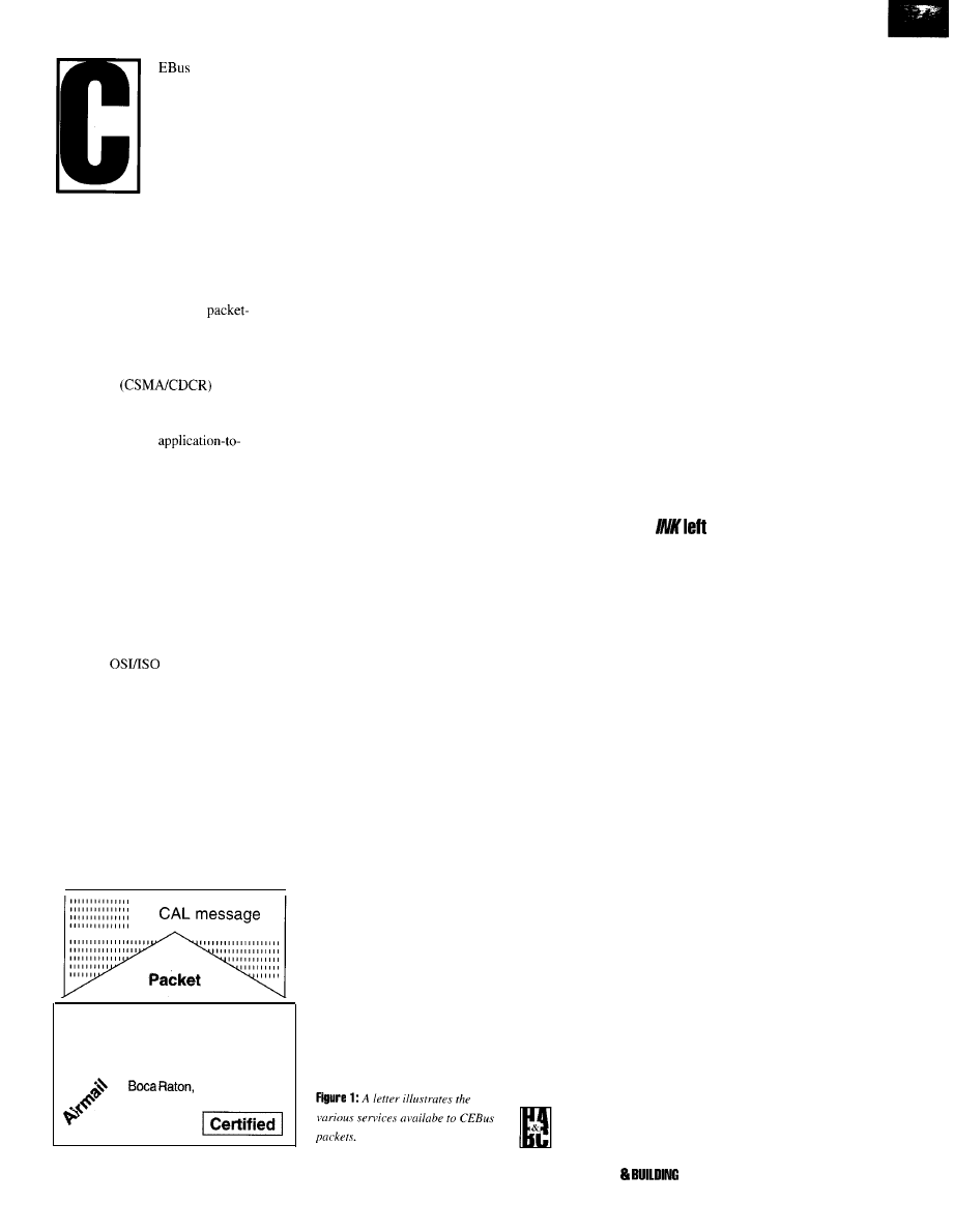
is the
Electronic Industries
Association’s (EIA)
open standard IS-60
describing a method
of communication
between electronic
products in the
home using five different media:
power line, twisted pair, coax,
broadcast RF, and infrared. A sixth
medium, fiber optic, has a section left
open and is undefined at this time.
CEBus is a complete,
oriented, peer-to-peer network using a
Carrier Sense Multiple Access with
Collision Detection and Collision
Resolution
protocol.
The CEBus standard defines every-
thing needed up to and including the
language used for
application communication called the
CEBus Common Application
Language (CAL).
In this article, I’ll introduce you
to packet construction and show you
how to create CAL messages that
control a CEBus light switch. Hang
on-or the details may swamp you!
CEBUS AND CAL
The CEBus protocol is described
using the
seven-layer model.
CEBus uses four of those layers:
application, network, data link, and
physical. Note the actual application
function (e.g., a light switch) is dis-
tinct from application layer protocol.
WHY CAL?
The CEBus application language
is a set of common language and data
constructs created to enable
Mr. Lightswitch
25 House St., Unit 19
FL 01011
CEBus for
the Masses
interoperability between products used in
residential automation. This interoperability
is available between different manufacturers’
products even without prior knowledge of
the products.
For example, information to control
Company X’s light module or stereo is
published by the EIA or the CEBus Industry
Council (CIC). This information is known to
the world without having to know anything
specific regarding Company X’s design
implementation of how they use a class A
amplifier to control a vacuum-encased,
electrothermal photon emitter-otherwise
known as a light bulb.
PACKET STRUCTURE
A CEBus packet frame can be broken
down into several parts: the Link Protocol
Data Unit (LPDU), the Network Protocol
Data Unit (NPDU), the Application Protocol
Data Unit (APDU), and the CAL message. I
describe these different parts using a mailed
letter (see Figure 1) as an example.
Figure 2 shows a breakdown of a packet
structure illustrating the different parts.
LPDUHEADER
The LPDU header contains the
control field and the source and destina-
tion addresses. In the letter mailing
scenario, the control field represents the
postal service used to send the letter. The
control field specifies the packet type,
PETER HOUSE
Picking up where other CEBus
articles in
off, Peter
introduces us to packet construc-
tion and CAL messages. By the end,
you’ll be able to control a real-live
CEBus light switch!
HOME AUTOMATION
CONTROL APRIL 1555
6 1
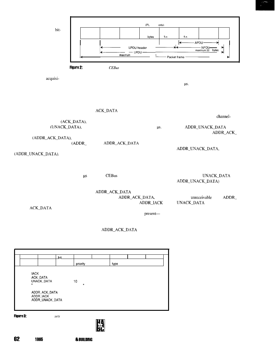
Packet structure
and RF
Preamble
Control
Destination
Source
NPDU
APDU
CAL
CRC
field
address
address
header
header
statement(s)
1 byte
4 bytes
4
bytes
bytes
packet priority, and service
class to the Data Link Layer
(DLL). Figure 3 shows a
oriented breakdown of the
control field.
The packet type is used to
select the form of DLL
41 bytes
service. This method roughly
corresponds to sending a letter
normal mail or with a return
The elements of a
packet are broken down into logical groups with size information
receipt requested. The DLL
handles all channel
tion, timing, and packet-receipt verification.
There are two classes of DLL service:
acknowledged and unacknowledged.
Acknowledged services expect a response
from the receiving nodes DLL and unac-
knowledged services do not. DLL packet
types include immediate acknowledge
(IACK), acknowledged data
unacknowledged data
failure (FAILURE), addressed acknowl-
edged data
addressed immediate acknowledge
IACK), and addressed unacknowledged data
Once a node acquires the channel, the
response from the receiving node is
considered part of the acquisition. The
acknowledge packet must start within 200
after the end of receiving a packet from the
requesting node. After the DLL receives the
transmit request from the application, the
DLL automatically handles all of the retries
and channel acquisition.
fields must be null. IACK signifies to the
The
services’ acknowl-
edge is an ultrashort packet with only an
NPDU header and a null information field.
The acknowledge packet’s control field
contains either FAILURE or IACK packet
type. The destination and source address
transmitting DLL the proper receipt of the
packet. FAILURE signifies that the receiv-
ing node’s DLL is operational but could not
pass the packet to its network layer.
The source address is optional in the
packet and can be omitted to
reduce channel-access duration. If the
transmitting node’s DLL does not receive an
IACK, a retry must begin within 600
If
the retry does not receive an IACK, the DLL
passes an error back up the protocol stack.
service supports
additional capabilities and enhances
reliability. A one-bit sequence number is
used by the receiving node to ignore
duplicate packets from the transmitting node
during a predetermined time interval defined
in the
specification. Because of this
added feature, the DLL accesses the channel
multiple times to make sure a packet using
service is transmitted.
receive an IACK, a retry must begin within
With the
the
receipt packet includes the
type in the control field. As well, the
destination addresses must be
which means that the source and destination
address must also be present in the request-
ing
packet.
If the transmitting node’s DLL does not
bit 7
bit 6
Sequence Service
number
class
5
bit 4
bit 3
bit 2
bit 1
bit 0
Reserved
Packet
Packet
Packet type (bit 2,1 and 0)
000
001
010
011
100
FAILURE
101
110
111
Packet priority (bit 4 and 3)
00
High
01
Standard
Deferred
11
Service
class
(bit 6)
0
Basic
1
Extended (undefined at this time)
Sequence number (bit 7)
Alternates each time a new packet is sent to a destination address
The LPDU header
the Data Link
Layer services and chooses the media access
priority.
600
If the retry does not receive an
IACK, the DLL relinquishes the
channel. It may reaccess the channel
and attempt to repeat the transmit
process without passing an error up
the stack. Only if the DLL exhausts
all of the predetermined
access attempts is an error reported.
has
similar capabilities to
DATA service without acknowledg-
ment packets or immediate retries. For
the DLL
transmits multiple copies of the pack-
et using multiple channel accesses.
Packets using a broadcast
address must use unacknowledged
services (either
or
since the
acknowledgments from the many
receiving nodes would collide and
result in
noise.
is the preferred
service for broadcast packets since
multiple packets using multiple
channel accesses are possible and
result in higher reliability.
Packet priority is used by the
DLL to determine the channel-access
priority timing. To gain access to the
channel, a node first listens for
channel activity (carrier sense). If
there is activity, the node waits until it
is finished. After a fixed amount of
time (based on priority) plus a random
amount of time, the node can attempt
to gain channel access by sending a
random-number packet preamble used
for contention resolution. If no
contention is detected, the packet is
sent. If contention is detected, the
node must wait for a new channel
access and transmission attempt.
The earliest a packet with the
highest priority can start is 1 ms after
the previous packet ends. The only
APRIL
HOME AUTOMATION
CONTROL
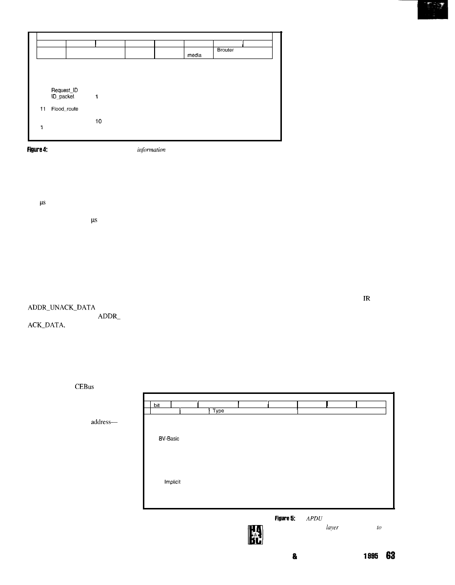
bit 7
bit 6
bit5 bit 4
bit 3
bit 2
bit 1
bit 0
Privilege
Routing
Packet
Extended
Allowed
flag
services
subfield
Privilege
Extended services
0
Unprivileged
0 No extended services
1
Privileged
1
Extended services octet to follow
Routing
Allowed media
00
0 This media only
0 1
Allowed media octet to follow
10 Directory route
Brouter
00 No brouter address
Packet flag
01
First brouter address presence
0
First packet
Second brouter address presence
Only packet
11
First and Second brouter address presence
The NPDU header describes network
including allowed media and how the packet is
routed.
two
exceptions
to this are for a packet
retry and acknowledgment. An
acknowledgment must start within
200 after the end of the packet to
be acknowledged. A packet retry is
sent approximately 600 after the
previous packet ends.
The sequence number is a single
bit field and is alternated for each
packet sent to a destination address.
This enables the DLL to distinguish a
received packet which is a copy and
not pass it up the stack to the
application layer. A packet could be a
copy due to a transmitting node using
with
duplicate packets or using
in which a sending
node does not hear the acknowledg-
ment and sends a retry.
DESTINATION AND SOURCE
ADDRESS
The destination address is four
bytes long giving
a potential
of four giganodes. The address is
divided equally into two logical
portions: system address and Media
Access Control (MAC)
usually called the house and unit
codes since most people are already
familiar with these terms.
If the unit code is zero, it is
considered a house broadcast
address-all nodes respond regardless
of their unit code. If the house and
unit codes are both zero, then all
nodes respond because this is
considered a global address. The
destination address has the same
formatting as the source address and
is transmitted in the same order.
The address is placed in the packet
from the unit code’s least-significant bit of
the least-significant byte to the house code’s
most-significant bit of the most-significant
byte. This seemingly reverse ordering offers
protection.
For instance, when the bits are actually
transmitted over the channel, the DLL
suppresses leading zeros to reduce the
transmitted time of the packet and improve
network throughput. Suppression of leading
zeros is possible because end-of-field
separator tokens are inserted by the DLL
before the packet is transmitted.
NPDUHEADER
The NPDU header specifies how the
packet is sent. Using the mail analogy, it
corresponds to using air mail, normal
delivery, or “in care of’ when a router
transfers a packet from one medium to
another (e.g., twisted pair to power line).
The NPDU header consists of six fields:
privilege, routing, packet flag, extended
services, allowed media, and brouter.
Figure 4 shows a bit-oriented
breakdown of the NPDU header.
The privilege field is restricted to
packets related to system management.
The routing field sends an ID
packet, request for the recipient to
send an ID packet, and selects
directory or flood routing from a
router. An ID packet is sent out by a
configured device whenever it is
powered on as a sign-on message or
when requested by a router. A router
uses the ID packet to keep a list of
nodes for each supported medium.
The packet flag field specifies if
this is the only packet or the first packet of a
multipacket message. Long messages can be
segmented into several packets since the
maximum packet length is 41 bytes, with
nine used for control and addressing. This
leaves 32 bytes for the complete NPDU
including any CAL statements.
The extended services field specifies
that additional NPDU bytes follow with
additional NPDU services.
The allowed media field tells routers
and brouters if they should route the message
to another medium. If you had a PL-to-IR
brouter, you probably would not want to
route the messages to IR because
is
typically used for hand-held remotes or
portable devices. If the allowed media field
specifies other media, an additional NPDU
byte specifies the allowed media.
The brouter field is used to control
routing of packets originating or terminating
on wireless media. A brouter is a device used
to cross between wireless and wired media.
For instance, you may want a hand-held IR
7 bit 6 bit 5
Reserved Mode
Reserved
1
Must be 1
Mode
0
variable length
1 BF-Basic one byte fixed
Type
000 Not used
001 Reject
010 Result
011 Receipt acknowledge
100
invoke
101 Explicit invoke
110 Conditional invoke
111 Explicit retry
bit 4
bit 3
bit 2
bit 1
bit 0
Invoke ID
Invoke ID
000
A three bit increment identifier used for packet tracking
001
010
011
100
101
110
111
The
header specifies how the
receiving application
should respond the
packet.
HOME AUTOMATION BUILDING CONTROL
APRIL
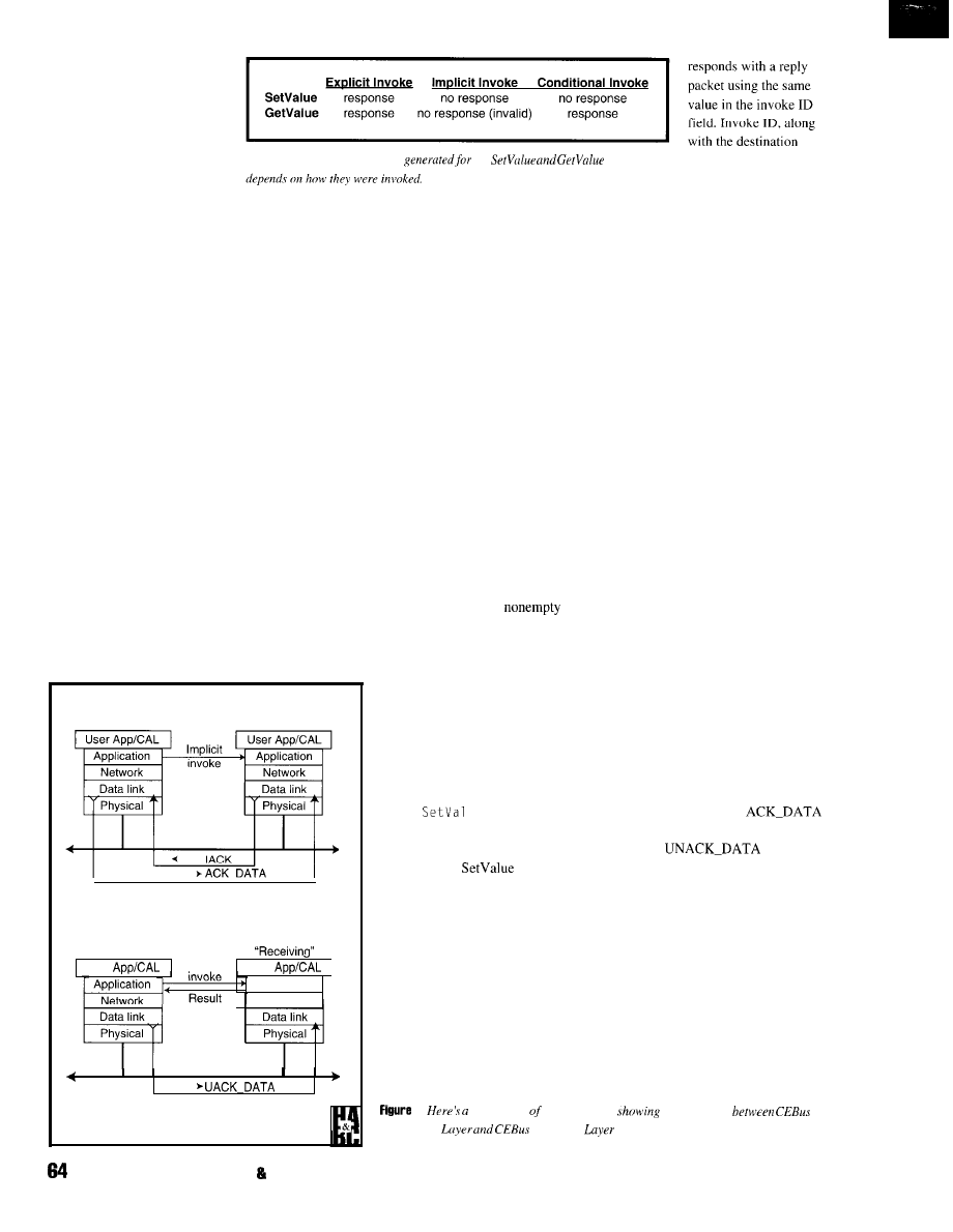
remote control to send
commands. Your TV could act
as a brouter to the VCR and
stereo via the power line.
A P D U H E A D E R
Table 1:
Whether a response is
the
methods
address, is used by the
The APDU header
specifies how and if the
receiving application layer
should respond to the packet. There are three
fields in the APDU: mode, type, and invoke
ID. In our mail analogy, the APDU is like an
RSVP at the bottom of the CAL message
letter. It tells the CAL interpreter on the
receiving end if it should respond (also
called
end-to-end confirmation)
or if there
are enclosures or a follow-up letter. Figure 5
shows a bit-oriented breakdown of the
APDU header.
The mode field tells you whether the
APDU uses multiple bytes. Most messages
use the basic fixed-length APDU mode.
Additional bytes are used for services such
as authentication or encryption.
Authentication is used by the receiving
node to verify the sending node’s authority
before the application layer passes the rest of
the APDU to the CAL interpreter. Encryp-
tion sends packets with the message secured.
The type field has seven values: reject,
result, receipt acknowledge, implicit invoke,
explicit invoke, conditional invoke, and
NODE A
“Sending”
NODE B
“Receiving”
Application layer-Implicit invoke
DLL-Acknowledged service
NODE A
“Sendina”
NODE B
User
Explicit
User
Application
Network
explicit retry. Reject is sent from the
receiving node’s application layer which
rejects the packet for some reason. Result
and receipt acknowledge are sent from the
receiving node’s CAL interpreter to tell the
sending node’s CAL interpreter that the
CAL command has been completed or
initiated with a complete response to follow.
Implicit invoke tells the receiving node
an application level response is not neces-
sary. Explicit invoke tells the receiving node
to respond with a CAL result response.
Explicit retry expects acknowledgment from
the receiving node’s application layer within
a predetermined amount of time-acknowl-
edgment could be either result or receipt
acknowledge. If none is received, the
application layer (not the application)
automatically retries the message.
Conditional invoke enables a device to
send a response only if it has a
result to return. If there is a result to return,
the response packet contains a result type in
the APDU header type field.
Conditional invoke could be used
with a broadcast address. A
response result would only be
initiated by a node matching the
conditional criteria since there
would be a result only if the
condition was true.
A
ue
CAL method
does not normally have a response.
If the transmitting node wants to
make sure the
method
was handled properly by the
receiving application’s CAL
interpreter, an explicit invoke can
be used. Table 1 demonstrates the
differences between the invokes
and their set and get values.
Invoke ID is a 3-bit field
incremented (and rolled over) for
each new transmitted message to a
destination address. The application
l
Application layer-Explicit invoke
DLL-Unacknowledged service
sending node so when
the results come back,
the sending node
matches the result application packet
to the proper command.
A transmitting node cannot stack
or send more than one command to a
receiving node until the receiving
node responds to the first packet. A
transmitting node sends packets to
multiple destinations and uses invoke
ID and the destination address to sort
out the result responses.
Let me take a moment to clarify
the distinction between the LPDU
packet type and the APDU type. The
DLL acknowledgment, if requested in
the LPDU packet type field, takes
place regardless of the APDU type
and without the application’s
knowledge if the application requests
acknowledged service.
As far as the application layer is
concerned, it is communicating with
the application layer of the receiving
node. The application layer is
unaware of any retries at the DLL
layer and the application is unaware
of any retries by the application layer.
Figure 6 shows two nodes-one
node is sending an implicit invoke in
the top example and the other is
sending an explicit invoke to the
bottom example. In the top example,
the application requests
DLL service, and in the bottom
example,
DLL
service is requested.
The application passes the packet
to the DLL. If the DLL cannot get an
IACK, only then does the DLL notify
the application of an error. When the
application layer calls for a response
from the receiving-node application
layer using the explicit invoke APDU
type, the receiving node returns a
result response packet to the original
sending node. This activity is separate
6:
breakdown
the OSI layers
the difference
Application
Data Link
services.
APRIL 1885 HOME AUTOMATION BUILDING CONTROL
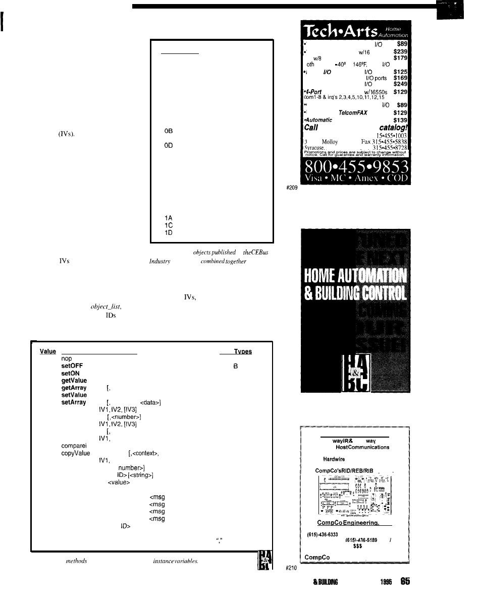
from the lower level DLL acknowl-
edgment services and can be used
regardless of the DLL service.
CAL DEVICE MODEL
CEBus uses a hierarchical model
to describe each node. Each node
includes two or more contexts, each
made up of two or more objects. Each
object contains one or more Instance
Variables
UNIVERSAL CONTEXT
The first context in every node is
called the
universal context
and has
nothing to do with normal operation
of the actual device. The universal
context is numbered 00 and controls
the device’s presence on the CEBus
network.
The universal context consists of
two objects: the node-control object
(object 0) and the context-control
object (object I). The
node control
object
has
to hold universal
device information such as the device
addresses, manufacturer name, and
other device management informa-
tion, while the context control object
has a single IV called
which holds a list of object
for
this context. Every context contains
Value Name
01
Node Control
02
Context Control
03
Data Channel Receiver
04
Data Channel Transmitter
05
Binary Switch
06
Binary Sensor
07
Analog Control
08
Analog Sensor
09
Multiposition Switch
OA
Multistate Sensor
Matrix Switch
o c
Multiplane Switch
Ganged Analog Control
OF
Meter
10
Display
11
Medium Transport
13
Dialer
14
Keypad
15
List Memory
16
Data Memory
17
Motor
19
Synthesizer/Tuner
Tone Generator
Counter
Clock
Table 2: The CAL
hy
Council are
to model
any real-world device.
one
or more
which control or publish
some aspect of the device. The universal
context is required in every CEBus-
compatible product.
Mnemonic Basic Svntax
Data
40
41
IV
42
IV
B
43
I V
BNC
44
IV [<offset>], <count>]
D
45
I V
BNC
46
IV [<offset>],
D
47
add
N
48
increment
IV
N
49
subtract
N
4A
decrement
IV <number>]
N
40
compare
IV2
BNCD
4 C
IV1 , <data>
BNCD
4D
IV1 , IV2
<object>]
BNCD
4E
swap
IV2
BNCD
52
exit
[<error
53
alias
<alias
54
inherit
IV,
D
55
disinherit
IV, <value>
D
56
if
<boolean> BEGIN
list> [else clause] END
57 do
<boolean> BEGIN
list> END
58
while
<boolean> BEGIN
list> END
59
repeat
<boolean> BEGIN
list> END
5A
build
<macro
BEGIN <message list> END
Methods in bold are required for minimum CEBus implementation; is F5 delimiter
Table 3:
CAL
perform operations on CAL
b
Text to Speech Board
serial
Temperature boards:
sensors
sensors plus 8 analog inputs
boards:
to
serial
Digital
ISA cards: 46
ports
96
192
ports
ISA Serial Board
I-Servo controller board
serial
Windows NT
Personal
Drapery Controller
fur our complete
support 3
08 E.
Rd
NY 13211
BBS
Home Automation
Two
Two
X-IO
Serial
Standalone Operation
connect options
Control hundreds of items with
system!
Inc.
For on-line information call our BBS
evenings/nights/weekends
Information line
voice
FAX
Don’t pay ‘big
any longer!
Get professional automation on a hobby budget.
means Computer Control!
ROME AUTOMATION
CONTROL APRIL

OTHER CONTEXTS
DATA TYPES
CEBus defines contexts which
can be grouped together to define
just about every device imaginable.
For instance, the lighting-control
context includes parameters for
defining a light switch. For a more
complex device like a stereo receiver
or a TV, several contexts containing
various objects can be combined.
For this article, I will focus on a light
switch available in a 500-W dimmer
version or a 15-A relay version.
Refer to the CAL model for the light
switch shown in Figure 6 and the
CAL object list in Table 2.
DO
57
WHILE 58
R E P E A T 5 9
BUILD 5A
AND
EO
OR
El
NOT
E2
XOR
E3
GT
E4
GTE
E5
LT
E6
LTE
E7
EQ
E8
NEQ
EA
ELSE
EB
LITERAL EC
DELTA
ED
P A R A M E T E R E E
NULL
FO (reserved)
MINIMUM
(reserved)
MAXIMUM
F2 (reserved)
DEFAULT
F3 (reserved)
DATA
F4
DELIMITER
F5
ESCAPE
F6
BEGIN
F7
END
F8
F A
F B
END-OF-FILE
FC (reserved)
Error
FD
Completed
FE
There are four data types
used in CAL: string, data,
numeric, and Boolean.
Strings are delimited by CAL
tokens or are at the end of a
packet. Data can be thought
of as array oriented. Numeric
is usually represented by a
string of ASCII numbers
(e.g., 3
h 30h
30h for the
number 100). Boolean is
always true or false. The byte
Olh is true and
is false.
PACKET BUILDING
The lighting context has two
objects. The context control object is
Table 4:
The CAL tokens are unique
the CAL
are used as
delimiters and to create programming constructs.
required to be the first object in
There are many things
you can do to a CEBus light
switch by sending it packets.
In this example, we turn it on
every context with the exception of
the universal context. The context control
which holds a list of the objects
in this
context.
Here, it would be 02 01 07 02,
showing this context has a CEBus object
type of 02 for the first (01) object and an
object type of 07 for the second (02) object.
light-control object to be CEBus compatible.
The CAL object 07 is an analog-control
object and has
as published by the
EIA. A manufacturer can choose to
implement only those
which make sense
for a particular product or add nonstandard
Unfortunately, there is no way for
anyone to know what nonstandard
are if
0
Unknown Context ID
1
Unknown Object ID
2
Unknown Method ID
3
Unknown IV Label
4
Malformed Expression
5
Macro not defined
6
Alias not defined
7
Syntax error
8
Resource in use
9
Command too Complex
10
Inherit Disabled
11
Value out of Range
12
Bad Argument Type
13
Power Off
14
Invalid Argument
15
IV Read Only
16
No Default
17
Cannot Inherit Resource
18
Precondition Complete
19
Application Busy
Table
CAL
codes are used indicate
various application-layer error conditions.
they
wanted to use them since the
are
not readily available until after the manufac-
turer chooses to publish them.
Only five
are implemented in this
light switch. The c r
a
1 ue
stores the
current dim value in percent (o-100). The
s
a v e
a 1 e
temporarily saves the
current_val ue.
The
step-rate
a n d
e
i e
set the ramp rate of the
ect manipulates the
ue
IV and controls the light.
METHODS, TOKENS, AND
ERROR CODES
CAL methods are used to perform
operations on CAL instance variables.
ue
and
ue
are probably the
most used and are shown in the example
packets later in the article. Table 3 shows a
list of the CAL methods.
CAL tokens are used to create program-
ming constructs and for delimiting data. The
Data
Delimiter
and
L i t e r a l
(EC) tokens are the most common tokens
found in CAL messages. The
Data
token is
used as a starting delimiter to separate array
data from the preceding information. The
De 1 i m i t e r
token separates portions of a
CAL message. The
L e r a 1
token precedes
string data. Table 4 shows a list of the CAL
tokens and their hexadecimal values.
Table 5 lists the error codes returned
from a CAL interpreter. These error codes
appear following an APDU with a type equal
to reject. In a multiple-part
mand, each part has a correspond-
ing APDU header and error code.
and off, set a dim level, ramp to a
level, read the serial number, and
change the device address based on
the serial number.
In the LPDU, we set the packet
priority to STANDARD and the
packet type to
DATA. All other fields are zero for a
control byte of
Remember the
sequence number is set by the
we don’t actually have control of it.
For this demonstration, we
assume the light switch has a house
code of 5 and a unit code of The
controller (us) has a house code of 2
and a unit code of
The NPDU byte has a value of
50h. This value calls for unprivileged,
directory-routed service on this
medium only.
The APDU is a single byte with
a value between
and
This
specifies a mode of basic one-byte
fixed and a type of explicit invoke.
The invoke ID increments for each
packet sent.
CAL MESSAGES
In the following examples, the
first bytes of each packet are the
same with the exception of byte
I,
where the invoke ID field is incre-
mented. The first
bytes (hex) are:
As you recall, the first byte is the
control byte and the next four bytes
APRIL 1995 HOME AUTOMATION
CONTROL
are the destination-address informa-
tion in right-to-left order, followed by
the source address, also in right-to-left
order. The next two bytes are the
NPDU and APDU headers.
ON, OFF, OR DIM
The on command uses the
Set
V a 1 e
method to send a value of
37htothe
feature-select
sets the current value to
by the
definitionof
feature-select.
The
bytes (hex) then are:
21 02 45 66
37.
The LPDU (50) shows a standard
The 21 is the ID of the lighting context, 02 is
the object number of the analog control, 45
is the
SetVal ue
method, 66 is the
ect
IV (i.e., ASCII “f’),
is
a delimiter, and 37 is an ASCII “7”. The
complete packet is:
OF01 00050001
0245
66 F5 37.
The response to this packet is:
Let Your Development Fly!
Choose
for your
design and get
your
Off the ground
of
schedule.
types of micro-
development
from
Call Hitex for your free demo
package and
how smooth
and efficient development with
professional
really can be!
sophisticated in-circuit emulators to remote
debuggers, monitors and simulators.
Complete solutions
available for:
‘2055 Gateway
400
complete 6051 family
San Jose, CA 95110
60266,
(406)
(406)
6633x.
packet priority and a packet type of
which does not require a
response from the DLL to acknowledge
packet receipt. The source and destination
addresses are reversed since the device is
now sending to the controller instead of
receiving from it. The NPDU (EO) is the
same as transmitted. The APDU has the
same mode, but the type field shows that it is
a result packet with the result of FE, which is
the completed CAL token.
Whew! I think
have someone get up
and turn the switch on next time.
The packet to turn the light off is
identical, except the value for the
feat
se 1 ec t
IV changes to 33h and the invoke
ID field for the APDU is incremented by
one. Setting the
ect
to 33h
s a v e a 1 e
IV before setting the
c u
r r e
a 1 e
to 0. This offers the feature
of having the light later restore to the
previous dim setting.
The result packet is the same, except
the invoke ID matches the invoke ID we
sent, which is what the invoke ID is intended
for. We could issue several commands to
this light switch. Since the result packets are
all identical, except for the invoke ID, we
can use this field to track the responses to the
packets sent. The complete sent packet is:
66
33
and the response is:
OF01 00020001
FE.
To dim the light, we set the c
r re n
va 1 ue
IV to the dim level desired. In this
example, we’ll use 50%. With a packet of 21
02 45 43
35 30, the 21 is the ID of the
lighting context, 02 is the object number of
the analog control. 45 is the
ue
method, 43 is the
current-value
IV
is a delimiter, and 35 30 is
ASCII for “5” and
or 50%. The complete
packet is:
43
35 30.
The result packet is once again identical,
except for the invoke ID:
OF01 00020001
HOME AUTOMATION BUILDING CONTROL APRIL 1995
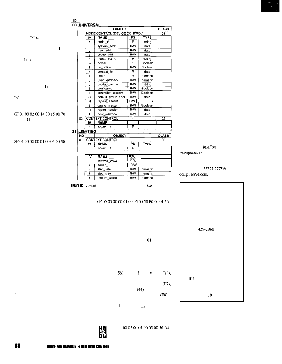
GETTING THE
SERIAL NUMBER
The serial-ii
instance
variable
be found in
the node control object of the
universal context in object
The packet reading the
se
ri
has the same
first
11 bytes as above and the
additional CAL command 00
01 43 73. The CAL command
is in the universal context
(00), object one (0
get the
value (43) of instance variable
(73).
The complete
send
packet is:
EB 00 43 73.
The result packet is:
D3 FE EC 54 30 30 30 30 30
3 0 3 0 3 0 3 0 3 5 3 9 .
Note the incremented invoke
ID in the sent packet and the
matching invoke ID in the
result packet. After the
complete token, there is a
delimiter token (EC) and the
serial number follows
CONTEXT
I
NO
31
B o o l e a n
list
PS TYPE
data
list
0
, data
32 ANALOG CONTROL (LIGHT LEVEL CONTROL)
07
TYPE
c
, numeric
value
numeric
A
light-control module would have
contexts,
four objects, and twenty-jive Instance Variables.
“T000000000059,” which actually matches
the serial number printed on the side of the
73 EC EC 54 30 30 30 30 30 30 30 30 30 35
switch!
39 F7 44 68 F8.
USING THE SERIAL NUMBER
Since the serial number is known from
the manufacturer’s label on the device, it
provides a good way to exclusively commu-
nicate with this unit for set-up purposes.
Normal communication uses the device
address after it is set and the device is
configured.
However, we will send a broadcast
message using the conditional invoke APDU
type and ask for the house code in return if
the serial number condition is met. The
packet this time is a little longer due to the
%-character serial number and the extra
bytes required to form the conditional
expression. Note the house code is an array
value and must be dealt with using the
methods and delimiters for handling arrays.
The control byte is the same as before
(OF), the destination address is the system
broadcast address (00 00 00 00) and the
source address is our address
00 05 00).
The NPDU header (50) is the same, the
APDU header is now the conditional invoke
type (FO), and we are dealing with the
universal context (00) and node control
object (01). The CAL message begins with
the IF token
the se
r a 1
IV (73
the Equal token (ES), a literal token (EC),
and the serial number. The begin token
the Get
A
r ray
method
the house code
IV (68 “h”), and finally the end token
wraps it up. Simplified-if the universal
context object
se r i a 1
is equal to
“T00000000059,” then get the array value of
the house code. The response packet is:
The packet to get the house code from
the module with the serial number equal to
“T00000000059” is:
OF01
FE F4 32 F6 00 05.
We actually played a sneaky trick on
the module. We asked for the house
code, which it dutifully sent, but we
then ignore the CAL portion of the
packet and get the source address,
which additionally gives us the unit
code without sending another packet!
SUMMARY
I
have known about CEBus for
the past five years and about six
months ago began developing a
CEBus product. It was difficult at first
because of the broad base of informa-
tion necessary before you can actually
do anything. This article includes a
healthy mix of the things that gave me
trouble or were hard to find and
decipher from reading IS-60.
Good luck on your CEBus
project.
Peter House is an applications
engineer with
Corporation, a
of the spread-spectrum
carrier components used to implement
CEBus on RF and PL media. He may
be reached at
SOURCES
The EIA CEBus Standard IS-60
is available from:
Global Engineering Documents
1990 M St. N.W., Ste. 400
Washington, DC 20036
(202)
Fax: (202) 33 l-0960
The CEBus dimmer module,
relay module, serial computer
interface, and the module’s
technical reference manual are
available from:
Home Automation Labs
Hembree Park Dr., Ste. H
Roswell, GA 30076
(404) 442-0240
Fax: (404) 4
1122
I R S
416 Very Useful
417 Moderately Useful
416 Not Useful
APRIL1995
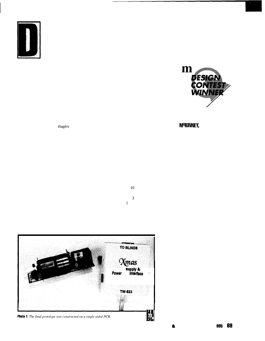
id you ever wish
you could control
the light blazing
through your
skylights on a
summer afternoon?
That collimated
beam sears the
plants, nullifies the air conditioning,
and slices anything that passes
through it like a carbon-dioxide laser.
Wouldn’t it be nice to have the same
command of your home’s natural
lighting that you have of its artificial
lighting?
This project was conceived from
just such need.
My wife Kim loves interior
designing and, as a result, things get
moved around from time to time. She
decided the entertainment
should be moved from its old location
and centered on the large window in
our living room. She claimed it would
balance the room and back light the
figurines in the cubbyholes.
The rearrangement did exactly
that as well as creating a magnificent
light sculpture! Unfortunately, it
introduced a contrast problem for
daytime TV viewing and rendered the
window’s two miniblinds nearly
inaccessible.
Operating the blinds became a
dreaded task which involved scaling
the furniture. To solve this problem,
one option was a commercial blind
motor. Rocker-switch operated, it
offered little more than manual
control and sold for around $300.
The Blind Robot
An
X-10 Miniblind
Automation Syste
Our other option of leaving the blinds
permanently closed solved the problem of
scaling furniture, but left us without our
recently acquired backlighting and light
sculpture.
Dissatisfied with those choices, I
pondered a “techno-cure” that would address
all problems involving the blinds, including
those throughout the rest of our home. At
this point in time, we were making rounds
twice a day to open and close them all.
My efforts to eliminate this chore,
ultimately coalesced in the X- Miniblind
Automation System or. if you’d rather,
XMAS, the blind robot. Photo shows the
final prototype and Figure illustrates the
simplicity of the system.
XMAS has control circuits and a drive
motor which fit within the blind’s header
assembly. An adapter unit connects to an
HERBERT
JR.
For Herb, home automation in-
cludes not only control of artificial
lighting, but also control of natural
lighting. The X-l 0 Miniblind Auto-
mation System offers individuals
the possibility to reach beyond the
confines of their home and stop the
impact of a blistering summer day.
Power
Une
Adapter
HOME AUTOMATION BUILDING CONTROL APRIL
1
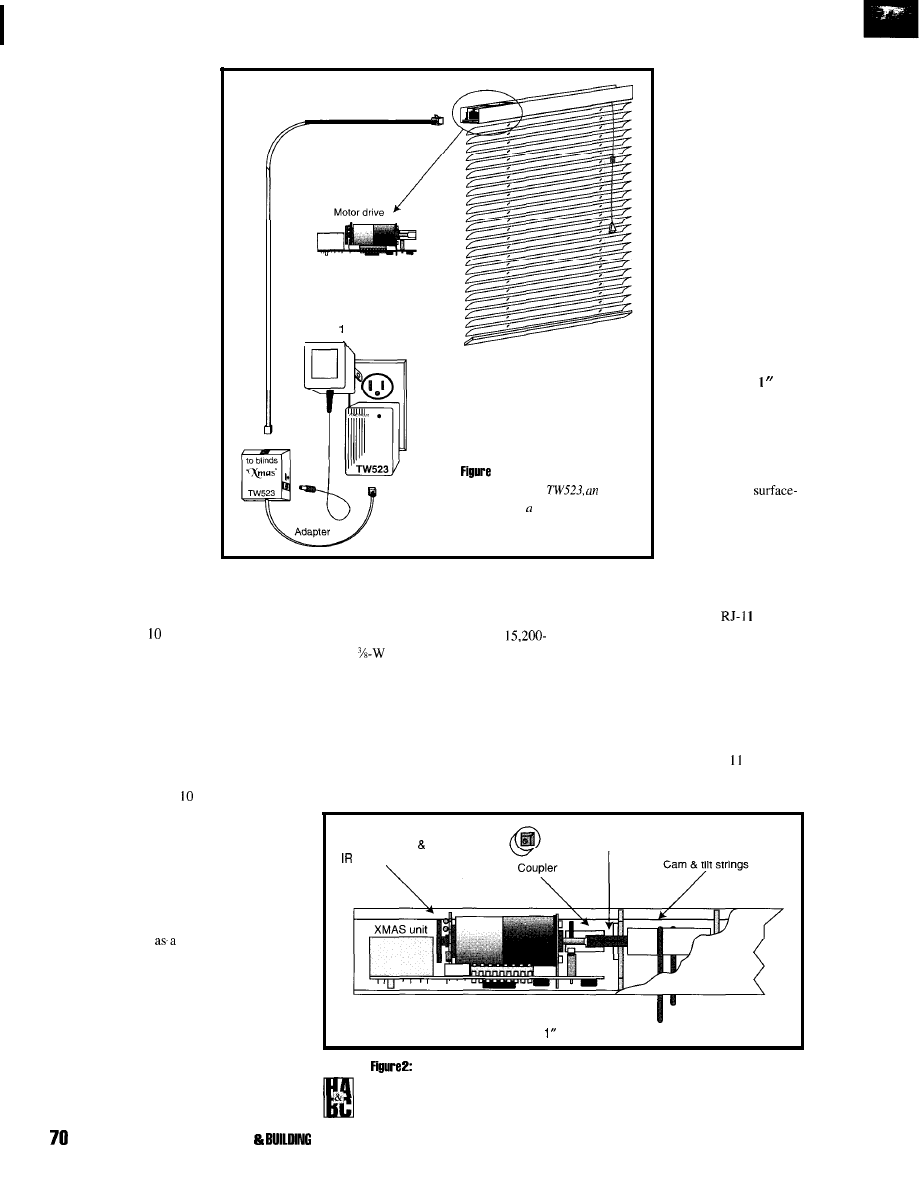
X- 10 interface module
(TW523) and power
supply. A modular cable
connects the adapter and
blind units. The cable may
be concealed in a tradi-
tional installation manner
along baseboards or run
through walls to outlets in
the window sills for a more
professional installation.
Up to 256 units may be
connected with each unit
having a unique address or
up to eight units may be
grouped into one unique
address.
XMAS operates
almost as a lamp module. It
interprets X- 10 on, off,
bright, and dim commands
as open, close, up step, and
down step, respectively.
There are 16 stages
between full up and full
down. Additionally, the
closed position (i.e., off) is
jumper selected between up
or down. Control and
programming of XMAS units can be
supplied by virtually any controller capable
of transmitting X- commands.
12
VDC,
A
,
1: The
basic system consists
of a motor drive,
adapter, and power supply
A set screw, which secures the coupler to the
motor shaft, also actuates the limit switches.
The motor is a 16-mm, 6-V,
RPM,
unit with an extended rear shaft.
To this shaft, I attach a photo-reflective disk
and sensing PCB to count revolutions.
Coupled to the front shaft is a 1670: 1
gearhead. The complete assembly develops
an intermittent torque of 14.2 oz.-in. and a
continuous torque of 7 oz.-in. This easily
The main PCB is
sized to 3” x 0.94”.
This form-factor just
squeaks in an installa-
tion of the smallest of
the headers I could find
from manufacturers’
data, which included 18
popular blinds from
many manufacturers.
The 3” length fits all
but custom-made
headers. Many
manufactures have
standardized on
header width or a
metric approximation,
but I found a lot of
variation here.
By using minia-
ture, SOP, and
mount devices, the
board accommodates
all the parts and still
offers axial alignment
between the motor shaft
and actuator rod in the smallest
header. The motor and
jack
placements are relatively fixed and
occupy 52% of the board space. So,
the remaining components are placed
for the tightest fit that routes without
DRC errors.
THE DEMON SEED
The humble beginning of XMAS was
as elementary as a surplus motor and a VCR
load-motor driver. Life was easy.
XMAS evolved from my knack for
taking something that is extremely simple
and making it much more complicated.
XMAS needed to be X- controlled and
considerably smaller. It also had to be totally
manufactured in my workshop.
I have tested (60” x
72”) coupled together
end to end.
I managed to keep all compo-
nents on grid, albeit a small one. The
mounting tabs of the RJ- connector
exceeds the load of two of the largest blinds
and forward motor support provide
After some thinking, I concluded that
Reflective
disc
source/sensor
Actuator rod
the primary goals for XMAS were that it be
cost effective, easily installed, universal, and
retrofittable. Twice, I completely designed it
in my mind-ach time allowing ample time
for the idea to pass
silly notion. But,
after the code was about half done, I finally
pulled out the stops and put it to the drawing
board. Kim wanted it next week. Sound
familiar?
THE MECHANICS
As Figure 2 demonstrates, the drive
Standard
header assembly
First, the worm and sector (drive) must be removedfrom the stock header. This
motor attaches to the blind’s actuator rod
is usually a pop-in plastic assembly in newer blinds. The XMAS unit then slides into the
with a coupler suitable to the model of blind.
header and mates with the actuator rod.
APRIL 1995 HOME AUTOMATION
CONTROL
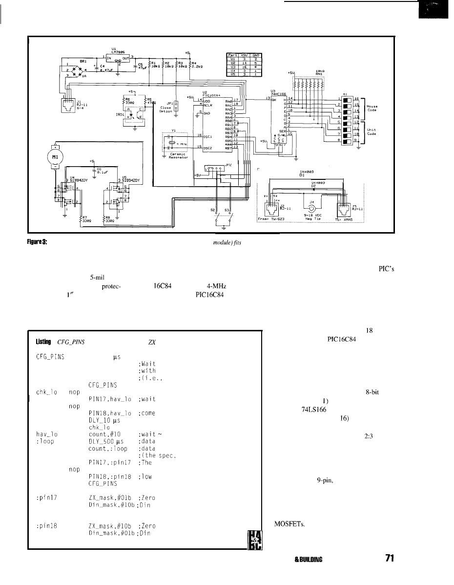
A d a p t e r M o d u l e
Thanks to small outline packaging, this circuit (excluding the adapter
onto a 2.8 square inch PCB
stand-off for the bottom-layer
THE ELECTRONICS
components. There is a
Lexan
The processor is a Microchip
sheet beneath for additional
PIC
clocked by a
ceramic
tion. I use 0.03 or 0.062” FR-4
resonator. Since the
has been
material in larger headers that may
covered
in prior issues of
INK,
I’ll go
need motor alignment.
straight into the details of this application.
1:
determines which pins are
and DATA.
The design takes advantage of the
in-circuit programmability. The applicable
pins may be accessed after assembly through
a jumper header. The EEPROM lets me
program the controller and revise firmware
on a completed unit without having to
remove the chip. This convenience, coupled
with the small footprint of the SO-
package, makes the
the perfect
controller for the job.
call LILY-10
sb
PIN17
for a quiet cycle
snb
PIN17
positive going ZX
sb
PIN18
both HI)
jmp
jnb
for 1st low to
jnb
along (either pin)
call
jmp
mov
5 ms longer to insure
call
bit time has past in case
djnz
is coincident with ZX
could allow this).
j n b
one that's still
jnb
is LX.
jmp
Figure 3 provides a schematic. The RA
port accommodates the ZERO CROSSING,
DATA IN, the revolution counter (RTCC),
and CLOSE option signals. The specific
house and unit codes are set by an
DIP
switch (see Table and read serially
through a
shift register by RA3.
The 74LS 166 (SO-
occupies Park
Place real estate, but it liberates five I/O pins
for needed functions. RB 0: 1 and
are
motor control bits paralleled to increase
drive current for future motor driver
improvements. (Note: The original driver
was a BAL6686, available only in small
quantities. It’s a
SIP, SOP IC
used
in
RC servo motors.)
mov
Crossing = Pin 17
mov
= Pin 18
ret
I’m pleased to say the board has already
been updated to accommodate two Siliconix
“Little Foot,” dual-complementary, power
This switch involved only minor
layout changes on one end of the PCB and
greatly improved performance.
mov
Crossing = Pin 18
mov
= Pin 17
ret
HOME AUTOMATION
CONTROL APRIL 1995
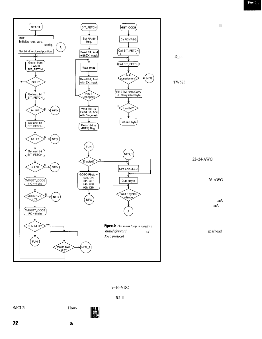
START
Determine: Input pin
step size, local address.
bit HI?
Set RA dir
Read RA, And
NFG
save in TEMP
0
NFG
Wait 3 cycles
silence
A
Set ENABLED Flag
interpretation the
as outlined in the
TW523 data sheet.
Bits 4 and 5 are CLK and LOAD,
respectively, for the shift register. Bits 6 and
7 read the LIMIT switches (normally open)
and are connected to the programming
header as well. NCLR is jumped to VCC
through the programming header. I had to
forego the recommended ESD protection on
due to lack of board space.
ever, with an awareness of this, in concert
with reasonable handling, it presents no
problem. All rebukes acknowledged!
Overall power for the system is
supplied by a
wall module. Input
power to XMAS is wired to the outside
terminals of the
connector. A bridge
was added to allow for polarity
reversal after which it is further
regulated by a simple 7805 circuit.
APRIL 1885 HOME AUTOMATION BUILDING CONTROL
The ZX and TX pins are rerouted to
the inside pins on the XMAS RJ-
connector. Diodes are placed in these
lines to match the signal levels to the
elevated ground.
A software routine determines
which inner RJ-11 terminals are ZX
and
This scheme allows for
straight- or reverse-wired modular
cables and a variety of AC/DC
converter options. However, it
requires a properly wired adapter for
the
and DC converter. This
seemed to be a worthwhile tradeoff.
To pacify the inspectors, I
specify a maximum of eight units
sharing a unique address. This
restriction is due to a limitation of the
wiring. Even though the recom-
mended supply is a power-limited
source, it can be easily replaced with a
heftier one. Considering a 100%
demand factor for these common
units, the number should be limited so
that the ampacity of the branch wiring
is not exceeded.
For a permanent installation in or
near a window,
telephone hook-up wire is highly
recommended. This standard allows
up to eight units to share a unique
address. When using only
modular cable, the maximum number
of common address units is reduced to
four.
One XMAS unit draws 62
under a normal load and 220
under a maximum, stall-condition
load. Fortunately, about the only way
to stall this hummer is on the motor
shaft itself through a bearing seizure
or such. Stalling from the
end produces gear failure. This test is
unnecessary. However, it yields about
$40 worth of catastrophic failure data
for those who feel they absolutely
need it!
THE SOFTWARE
To begin, let me confess I’ve
never been accused of generating tight
code. I welcome any criticism that
advances my capabilities.
Because of having primarily a
hardware background, I expected that
coding would be more difficult,
especially since this was my first PIC
project. I chose the Parallax tools to
take advantage of my residual
assembler experience, which
expedited the task.
As the flowchart in Figure 4
indicates, the software consists of a
main loop which lies in wait for a start
code from the TW523. It then snares
and interprets house, unit, and
function codes, and subsequently
directs calls to peripheral control
routines. A multifunction interrupt
routine initially calculates step sizes,
then monitors motor movement and
effects limit stops.
The
I N IT
routine is a little more
involved than the flow diagram
indicates. After initializing INTCON,
OPTION, port direction registers, and
the variables, the
I NIT
routine calls
(Listing 1).
P I N
determines which of pins 17 and
18 are the ZX and
signals for
later use in the B
I T-FETCH
routine.
reads the TW523. A call to
R
reads the local
serially from
the shift register into
Paddr. It
is later
compared with the TW523 received
code.
I N IT
then runs the motor between the
high and low limits while accumulating the
number of revolutions betwixt the twain with
the RTCC using the RT interrupt (the
revolutions accumulate in the
NT
routine).
RTCC rollovers are stored in the upper
byte of
Ra n g e while
RTCC leftovers are
placed in the lower byte of
Range. Range is
then divided by 16 to obtain St p i z, which
is later loaded back into the RTCC to
generate the interrupt that stops the motor
after each step of bright or dim.
I N I T
has already read the JP 1 jumper
to decide which way to drive the motor to
the first (open) limit. After reversing the
motor, it leaves the blind in the closed
position when the second limit has been
found. Notably, the routines
P
and
always correspond to bright and
dim, respectively, but on and off depend on
the
condition. On is the center, open
position and off is selected between the up or
down position with
CAVIAR CAVEATS
From the start, I searched for a
small-outline motor driver since
board space was so limited. My eventual
discovery of the
MOSFET
drivers was as appetizing as a tin of fine
Russian roe-the Siliconix chips aren’t as
expensive, but they’re almost as rare in
quantities under 500.
I finally obtained some samples and
performed the upgrade. The pair of
significantly reduce motor run-on after
removing the drive signal. The free-wheeling
diodes, coupled with the fact that the
side
can conduct during the
motor’s off state, effectively produce
automatic braking.
The improvement was so dramatic that
I removed a call to the
BRAKE
routine that
previously terminated the
STEP
function.
This enabled the main loop to run nearly 200
ms faster in the
STEP
mode. The result was
more clearly defined steps and almost a
three-fold increase in the continuous step
rate.
I chose not to incorporate the X- all-
units-off and -on commands into my
personal units. I may include those com-
mands in the future strictly for compatibility.
When
technology stabilizes and
miniaturizes (hopefully), I will then
Get Your Copy of The
Best Source of Home
Automation Products
Absolutely Free.
Largest Selection of Home Automation products in the World
Call
for Free
64
page Color Catalog
(800-762-7846)
Hundreds of hard-to-find home automation and wireless control
products. Computer control of your home, security systems, sur-
veillance cameras, infra red audio/video control, HVAC, pet care
automation, wiring supplies and much more
H
O M E
S
Y S T E M S
, I
N C
.
151
Dr. Ste M6 Costa Mesa CA 92626
Questions
Fax
What Do You Need
To Be a
WINNER
In the
Fast-Growing
Home Automation Industry?
Find out when you join the
Home Automation Association
Clip and fax today for more information.
Name
Title
Company
Address
City
State/Zip
Phone
Fax
Home Automation Association
Fax:
E-mail:
Voice:
HOME AUTOMATION BUILDING CONTROL APRIL 1995
73
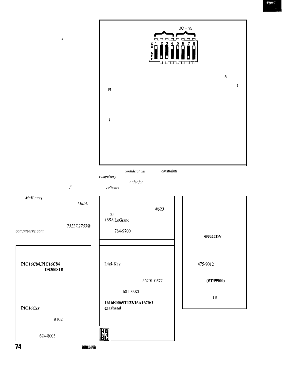
endeavor to make this now-simple affair yet
more complicated.
Although I have not actually tested 256
of these units connected to miles of cable, I
suspect that the system succumbs to the
same pitfalls as many distribution schemes.
No doubt, cable capacitance eventually wins
over rise times. Therefore, the number of
units that can be connected to the same
TW523 is not guaranteed.
Last, but not least, what can I say?
When the power goes off, you’re just plain
outta luck!
AND TO ALL A GOOD NIGHT...
I
initially tried doggedly to dismiss this
XMAS idea as cornier than The Clapper, but
climbing speakers to close the blinds had
become untenable. After contemplating other
possible arenas for XMAS such as office
buildings, schools, passive solar control,
green houses, hospitals, and homes of
handicapped individuals, I continued my
quest. At approximately $120 per blind
(excluding power and control), we consider
our dilemma totally resolved.
Perhaps, The Clapper isn’t so corny
after all!
For now, I’ll rest well knowing that
XMAS defends our privacy “as visions of
sugar plums dance in my head..
Herb
is a former Hewlett-Packard
service engineer who currently owns
Technics, a small service consulting and
engineering business. He enjoys working
with all forms of automation and process
control. He may be reached at
REFERENCES
Reference
Manual, and
Microchip Technology, Inc.
2355 West Chandler Blvd.
Chandler, AZ 85224
(602) 786-7200
Fax: (602) 899-9210
Development Tools
Parallax, Inc.
3805 Atherton Rd.,
Rocklin, CA 95765
(916) 624-8333
Fax: (9 16)
H C = A
Switch settings
HC
1
2
3
4
5
6
7
UC
A
ON
OFF
OFF
ON
OFF
OFF
C
ON
OFF ON
D
ON
OFF ON
E
OFF ON ON
F
OFF ON ON
G
OFF ON
OFF
H
OFF ON
OFF
OFF OFF
OFF
J
OFF
O F F O F F
K
OFF
OFF ON
L
OFF
OFF ON
M
ON ON ON
N
ON ON ON
0
ON ON
OFF
P
ON ON
OFF
ON = UP = INACTIVE
ON
OFF
ON
OFF
O N
OFF
ON
OFF
ON
OFF
ON
OFF
O N
OFF
O N
OFF
ON
OFF OFF ON
ON
OFF OFF OFF 2
ON
OFF ON ON 3
O N
OFF ON
OFF 4
OFF ON ON ON 5
OFF ON ON
OFF 6
OFF ON
OFF ON 7
OFF ON
OFF OFF 8
OFF OFF OFF ON 9
OFF OFF OFF OFF 10
OFF OFF ON ON 11
OFF OFF ON
OFF 12
ON ON ON ON 13
ON ON ON
OFF 14
ON ON
OFF ON 15
ON ON
OFF OFF 16
OFF = DOWN = ACTIVE
Table 1: Cost
and layout
made a DIP switch and negative logic
for
address setting. The address is encoded by the switch settings.
After serializing, it
assumes
the correct
direct comparison
with the received code. This eliminates the need
for a
conversion table.
X-10 Technical Note: Two-Way,
Power-Line Interface Model
X- (USA), Inc.
Ave.
Northvale, NJ 07647
(201)
SOURCES
Corp.
701 Brooks Ave.
P.O. Box 677
Thief River Falls, MN
(800) 344-4539
Fax: (218)
motor
Micro Moe
742 Second Avenue South
St. Petersburg, FL 33701
(8 13) 822-2529
Fax: (8 13) 82 l-6220
Mouser Electronics, Inc.
12 Emery Ave.
Randolph, NJ 07869
(800) 346-6873
Fax: (201) 328-7120
Siliconix
Rep, Inc.
Temic Group
P.O. Box 728
Jefferson City, TN 37760
(615)
Fax: (6 15) 475-6340
BAL 6686
Futuba Corp.
4 Stedebaker
Irvine, CA 927
(714) 455-9888
I R S
419 Very Useful
420 Moderately Useful
421 Not Useful
APRIL 1995 HOME AUTOMATION 8
CONTROL

he Remote
Controlled Speaker
Selector (RCSS)
addresses the
challenge of
creating a conve-
nient, multiroom
listening environ-
ment for the home. Most stereo
systems have manual A/B speaker
selection which provides music to one
of two rooms or both rooms simulta-
neously (A+B). If that’s not enough,
an external speaker selector can be
added easily.
But what if you’re outside in the
pool and the urge to swim laps to
“Born in the USA” suddenly grabs
you? In this scenario, you must go
inside, negotiate a polished kitchen
floor with wet feet, and switch the
stereo to play over the pool speak-
ers-not exactly the dream of home
automation.
Some high-end systems address
the problem of multiroom listening by
using proprietary modulation
schemes. These schemes multiplex
audio and two-way data over
installed coax to each room. The
problem with this solution is that a
perfectly good stereo system has to be
replaced.
Alternatively, a few add-on
devices can be used with existing
stereo systems in one way or
another-some use X- 10, infrared, or
combinations thereof. However, these
systems are fairly expensive, often
compromise amplifier safety by
switching only one side of the output,
or lack user feedback, which is
essential in remote switching.
DEVICE DESCRIPTION
The RCSS is an add-on
stereo component designed for loud-
speaker selection from virtually any
infrared (IR) remote
An
innovative learning algorithm and
high-integration microcontroller make
the RCSS “smart” as well as inexpen-
sive with its low parts count.
The RCSS can be used with
the-shelf IR repeater systems for
separate room-speaker selection. This
lets a listener select speakers from
whatever room they are in without
A Learning
Remote-Controlled
Speaker Selector
having to physically make a selection at the
amplifier or receiver location. Since most
existing stereo systems can already be
remotely controlled with an off-the-shelf IR
repeater, the RCSS adds the speaker-select
function that most stereo systems lack. With
the RCSS, the user obtains multiroom
listening convenience while retaining their
existing audio equipment. A diagram of the
RCSS is provided in Figure 1.
SYSTEM OVERVIEW
Specific highlights of the RCSS
include:
l
Learning algorithm-The RCSS offers
maximum flexibility. It can be controlled
by virtually any IR remote controller,
regardless of manufacturer. Low-cost
generic IR remotes can be
used
for
selection control.
l
Four speaker pairs-Four independent
speaker pairs can be selected with the
RCSS.
l
Manual operation-A front-panel push
button provides manual selection of
individual speaker pairs as well as
pair combinations for two-room listening.
l
Indicator lights-Four green
give
visual status of speaker selection(s). A red
LED marks learn status (on = learn
mode). The red LED flutters on initial
to show that the RCSS needs
programming.
l
Confirmation tone-A dual-frequency
confirmation tone is sent to the
selected speaker pair before the
music source is switched in. The
SCOTT
CLARK
Scott and Clark set out to find
remote-speaker selection without
replacing their current stereo
system or spending too much
money. The ultimate solution: an
add-on component with an innova-
tive intrared learning algorithm
and a highly integrated
microcontroller.
HOME AUTOMATION BUILDING CONTROL APRIL 1
7 5
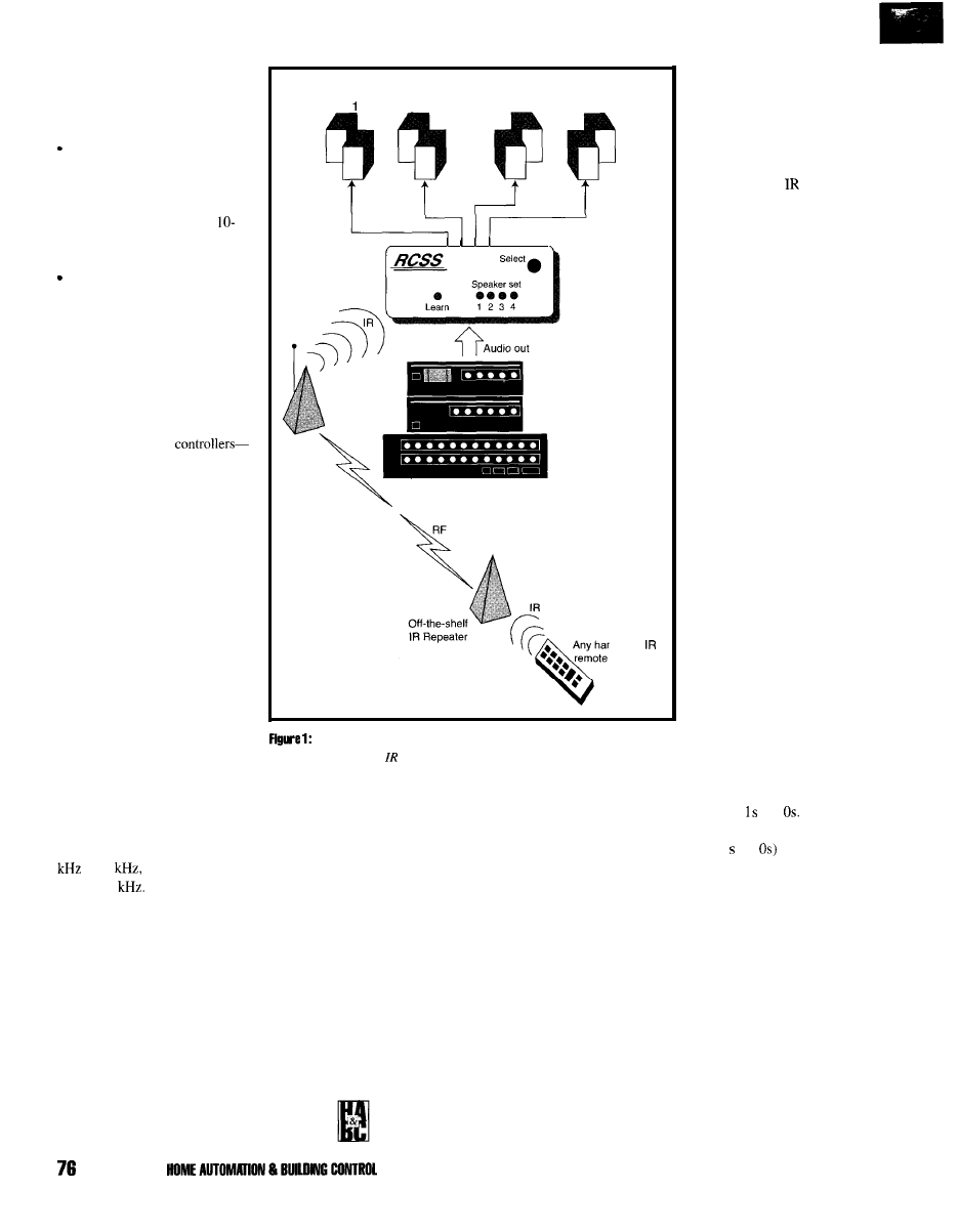
confirmation tone provides an
audible indication that the
correct speaker pair has been
selected.
Program retention-RCSS
remembers the commands it has
learned when power is
interrupted or the unit is
unplugged. A replaceable
year lithium coin cell provides
power backup.
Low cost-The cost for the
electronic portion of the
prototype was under $50.
DEVELOPMENT
OBJECTIVES
A major design goal in the
development of the RCSS was to
make it compatible with most
hand-held IR remote
no one needs another remote to
add to their collection. And, most
controllers have extra, never-used
buttons. Thus, developing a
device capable of learning and
recognizing existing IR controller
codes was central. Although a
simple sampling method could
work, the memory requirements
for even a single IR code are
relatively large, even with the
application of rudimentary
compression techniques
(INK 29).
IR CONTROLLER CODES
When you push a button on a
remote controller, the remote
emits a series of infrared bursts.
The bursts, which amount to
switching a pulse carrier on or off,
Speaker set:
2
3
4
Stereo system
nd-held
controller
This conceptual diagram shows how the RCSS can be used in a home
environment. Low-cost
repeater transmitters are located with each speaker
pair.
carry the code corresponding to the button.
Pulse-carrier frequencies range from 25
to 60
with the most common
around 38
The carrier bursts usually
last from 0.5 to 2 ms in duration and
correspond to a bit in the function code. An
entire code sequence may have 12 to 32 bits
(or bursts), so the code frame time would be
on the order of tens of milliseconds.
Most remotes also have a common
sequence marking the start of all the codes
they transmit. It essentially acts as a wake up
preamble. The modulated information sent
by the remote is demodulated by the
receiving device into an asynchronous
stream of binary highs and lows which
generally contains a preamble sequence,
manufacturer and device information, and
the specific function command.
Manufacturers can and do use different
schemes for embedding information in the
infrared flashes-there are no industry
standards for encoding. Most use some form
of pulse-width modulation which conveys
bit information according to carrier-burst
duration. The bits can be represented by the
actual bursts or by the time between them.
Manufacturers also have unique
schemes for repeat functions. Say you want
to crank up the TV volume. You hold down
the Volume+ button. One manufacturer’s
remote transmits the entire
Volume+ command repeatedly,
while another sends the Volume+
command once
followed by a shorter
repeat sequence for as
long as you hold down
the button. Figure 2
shows the start of a few
typical received
codes.
Though there are
undoubtedly countless
control codes, with a
learning device, it does
not matter. For the
RCSS, the only thing
that matters is that it
recognizes a learned
button when it is
pushed again. To do
this, the RCSS has to
pick apart and store the
necessary elements of a
button’s code sequence.
In general, the code
sequences follow these
criteria:
l
Code sequences
always follow the
format: preamble,
space, code informa-
tion
l
The preamble is at
least three times
longer than a space
l
Space defines the
duration for a binary
0 (arbitrarily
assigned)
l
Space is always the
inverse polarity of
binary and
That is, when bits (1 and
are
represented during the times the LED
is modulated on, the space between
bits occurs when the LED is off.
Conversely, if the bits are represented
during the times that the LED is off,
then the space between bits
occurs
when the LED is on.
These generalizations hold true
for the vast majority of infrared codes.
In the simplest terms, the RCSS
algorithm measures the duration from
one transition to the next, producing a
count. The count represents both the
time that the LED is modulated with a
burst and the time between bursts.
APRIL1995
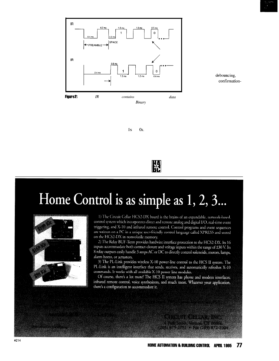
The count is stored,
another event is timed, and
the new count is subtracted
from the previous count.
From this result, the
program determines
whether the bit of code
information is a 1 or a 0,
and the process repeats for
succeeding bits.
The algorithm has
been developed based
upon the following
protocol generalizations:
code with Information in high pulses:
1
1
as many as 32 bits
code with information in low pulses:
1
+ - P R E A M B L E
SPACE
l
The first and second
counts, essentially the
preamble, don’t matter
and can be discarded
The typical
code sequence
pulse-width modulated
in
either the low or high portion of the pulse train.
bit information is
encoded in the pulse-width variations. Fixed-width pulses correspond to
spaces between bit information.
l
The absolute difference between a
low and high count following the
preamble is significantly greater
than 0 for a binary 1 and near zero
for a binary 0.
Using these assumptions, the RCSS
algorithm produces a compact binary
representation of the incoming remote
code, regardless of the carrier frequency, the
bit rate, or the format for
and
In the program, each absolute differ-
ence is checked against a tolerance value for
translation into either a 1 or a 0. The bit is
then packed into a four-byte holding
location. Each IR remote button
learned is represented in 32 bits
(whether it needs that much room or
not) to keep the algorithm simple.
Occasionally, more than 32 bits
are required, but the majority of
controllers operate at 32 bits or
fewer.
FIRMWARE
The general development
approach of the RCSS was to do
as much as possible in firmware
including switch
IR
signal recognition,
tone output, and front-panel
indication. This approach not
only minimizes cost by reducing
parts count and circuit-board real
estate, but also facilitates the
development of an intuitive user
interface. The interface is
important because most of the time the user
would not be within sight of the RCSS.
Additionally, the intuitive interface bolsters
user confidence in the training process and
front-panel operation.
FIRMWARE OPERATION
Figure 3 is an overall flow diagram of
the RCSS software. The program starts at the
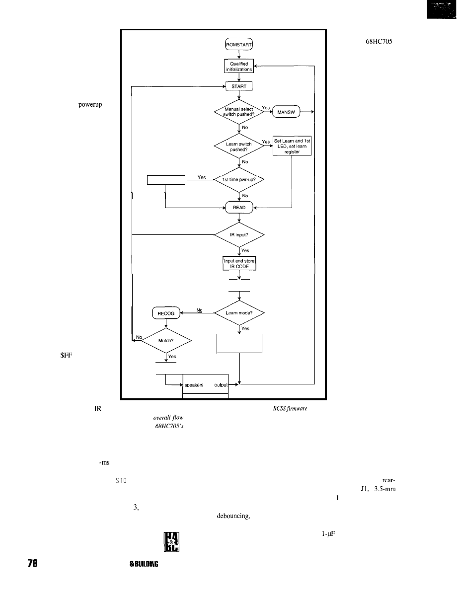
beginning of ROM (location
$0200) with a series of
qualified initializations. The
ports are defined, then port A
is read. If the lower four bits
of port A are cleared-a
normally illegal state-thenthe
T E M P 2
register is loaded with
$FF as a first-time
flag for use later in the
program. Other qualified
initializations include clearing
the IR code storage locations
(C 0
DE),
common registers, and
count variables. This portion
of the program is recycled by
different routines to conserve
Flutter Learn LED
program memory.
After qualified
initializations, the computer
operating properly (COP)
register is reset. This paves the
way for a series of bit-level
interrogations. First, port A,
bit 4 is checked for manual
switch closure. If the switch is
closed, control is transferred to
the
MANSW
routine.
4
NO
Next, the Learn switch,
bit 1 of port B, is checked for
closure. If it has been pushed,
both the first LED (speaker set
1) and the Learn LED are lit.
The program then monitors for
IR input. If the Learn switch
has not been pushed,
T EM P 2
is
checked for
and the Learn
LED is toggled if it is $FF.
Finally, bit 0 of port B is
checked for IR input. If none
is present, the program returns
to reset the COP register. It
continues this loop until
is
detected at bit 0 of port B.
When port B, bit 0 finally
goes low-signaling IR
input-program control is
Figure 8:
A modular approach was used in the development of
when
possible. This
diagram shows that some routines are recycled to make
best use of the
tiny 0.5 KB of ROM and 32 bytes of RAM.
transferred to the
READ
routine. The IR data
is serially sampled at a 0.1
rate and
stored in indexed code RAM locations. After
input, control is transferred to the
RE
STORE
Move CODE to
storage location, light
next LED
SWOUT
Switch in selected
and
confirmation tone
routine.
STORE
first checks for learn mode. If
the learn register,
TEMP2,
is set to 1,
2,
or
4,
code bytes are transferred to the appropri-
ate storage locations. If not in the learn
mode, program control is transferred to the
RECOG
routine.
R EC 0 G
sequentially compares stored
bytes with the code read in. If there is no
match, the program returns to the beginning
where sequential checks are performed
again. If there is a match, control is
transferred to the
SWOUT
routine.
SW
0 UT
performs speaker and source
relay switching and
and output
confirmation-tone generation. After
the switching is complete, the
program returns to
ST ART
The program fully
utilizes the
microcontroller to
provide IR code
learning and recognition
as well as an intuitive
user interface. All RAM
and most of the ROM is
used. Real-time
interrupts are not used
because of RAM
limitations and they
simply are not needed.
The microcontroller
operates in the
microsecond world,
whereas IR codes are in
the millisecond domain.
HARDWARE
The hardware
components and layout
are designed for a high
degree of integration,
low parts count, and
short wiring runs. All
components are
available from several
sources.
The RCSS is
designed so that all
wiring connections are
made at the rear panel,
with the front panel of
the aluminum enclosure
reserved for operating
controls and indicators.
Construction is by hard
wiring, but the circuit
board may be removed
from the case by
unfastening the front
and rear panels. This
design provides for high
reliability while using
commonly available
components. Figure 4
shows the schematic layout.
POWER SUPPLY
Power enters the RCSS at
panel power connector
a
phone jack. A N4004 diode protects
the circuitry from reverse voltage
should a power source of opposite
polarity be plugged into the rear
panel. A
ceramic capacitor filters
the power input, and a MOV provides
APRIL 1995 HOME AUTOMATION
CONTROL
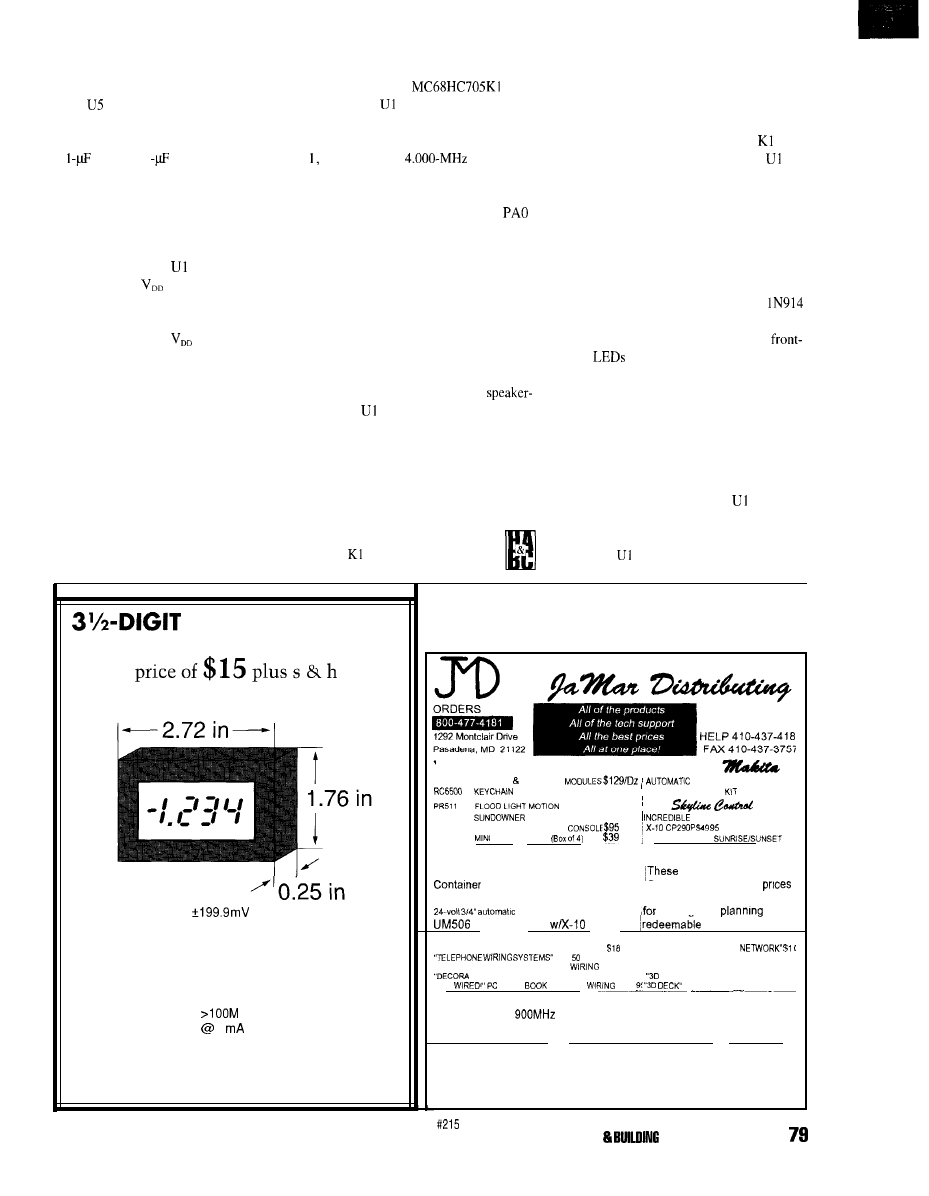
surge protection for voltage spikes
over 33 V to the voltage regulator
(U5).
is a 5-V linear regulator in a
TO220 package. The 5-V output of
the regulator is bypassed by both a
0.
and a 0.01
capacitor.
Battery backup and switchover is
accomplished by U4, a Maxim
MAX704 supervisory circuit designed
for use with microprocessors. During
normal operation, U4 simply passes
the 5-V supply to the
microcontroller
pin. However, if
the 5-V supply drops below 4.4 V, U4
holds the microcontroller reset pin
low and switches the
supply to a
3-V lithium battery.
This scheme provides backup
power for the microcontroller RAM.
Thus, the microcontroller RAM is
nonvolatile and its contents are
retained in the event of a power
outage. Even frequent, short-duration
power interruptions do not signifi-
cantly reduce the battery’s life below
its expected shelf life.
All other power connections are
made to the 5-V regulator output.
MICROCONTROLLER
U I is a Motorola
microcontroller.
receives data from the
infrared module at port PBO. The Select and
Learn switches are read at ports PA4 and
PB respectively. A
crystal
clocks the microcontroller. Port PA6 is
configured as an output to control the input
audio-source relay driver. Output ports
through PA3 control the four speaker audio-
output relay drivers. Output port PA5
generates a confirmation tone, which is sent
to one of four speaker outputs. Output port
PA7 drives an LED driver for learn-mode
indication. The IRQ line is pulled up
(disabled).
Under software control, the
microcontroller reads and learns infrared
codes, or reads IR codes and selects
pair outputs.
also disconnects the audio-
source input, generates a confirmation tone,
and reconnects the audio-source input when
a new output is selected.
RELAYS AND LEDS
Relays Kl-K6 are all Aromat
JW-series relays, which can switch
up to 5 A.
and K2 are input
relays that have two form-C contacts each,
thereby enabling the hot and ground signals
from both channels of a stereo amplifier to
be disconnected during confirmation-tone
generation. During tone generation,
and
K2 select local ground and tone from
port PA5 to be sent to the output relays.
K3 through K6 all have two form-A
contacts, which switch only the hot (+)
signal from each channel input, either on or
off. All relay drivers are PNP transistors
contained within U2 and U3 transistor
packages. The PNP relay drivers are
protected from inductive kickback by
diodes across the relay
coils.
The output
relay driver U2 also drives four green,
panel
for indicating front-panel output
selection. One of the U3 transistors drives
the red LED for front-panel indication of the
learn mode.
SWITCHES, HARDWARE,
AND IR MODULE
The front-panel, momentary push-
button switch Select is read by
to
sequentially select the speaker output from
the front panel. The rear-panel Learn switch
is read by
to put the unit in learn mode.
LCD PANEL METER
-Available now at an unheard of
N e w ! N o t s u r p l u s !
Specifications:
Maximum input:
additional ranges provided through
external resistor dividers
Display: 3%digit LCD, 0.5 in. figure height,
jumper-selectable decimal point
Conversion: Dual slope conversion, 2-3
readings per sec.
Input Impedance:
ohm
Power: 9-l 2 VDC
1
DC
Circuit Cellar, Inc.
4 Park Street, Suite 12, Vernon, CT 06066
Tel: (203) 8752751
Fax: (203) 872-2204
X-IO
SALE THIS MONTH ONLY
LAMP WALL SWITCH APPLIANCE
DRAPERY OPENER
REMOTE&BASE
$ 1 9
COMPLETE SYSTEM
5349
DETECTOR $38
SD533
$12
SOFTWARE UPGRADE FOR
PA5800
PERSONAL ASSISTANCE
MC460
CONTROLLERS
EASIER TO EDIT 8
STARTER KITS
Get ready for Spring
Drip watering landscape kit
drip watering kit
28.99
kits are expandable
14.99 Complete catalogs and
Drip soaker vegetable kit
28.99 ‘are sent with kits or send $5
anti-syphon valve
24.24
catalog and
guide
to control valve
19.97
on first order
BOOKS. LITERATURE AND SOFTWARE
“A
PRACTICAL GUIDE TO HOME AUTO
MA
TION’
99
“THE HOME AUTOMATION
52
“HOW TO TROUBLESHOOT PREMISE
SYSTEMS FASTER AND MORE EFFICIENTLY
$3 95
HOME CONTROL TECHNICAL MANUAL
5.3 99
LANDSCAPING’ (WINDOWS) 579 95
“GET
BASED
ON HOME
$29
(WINDOWS)
579 95
NEW
KX-TQ500
CORDLESS TELEPHONE
$199
20053
I-BUTTON REMOTE CAR STARTER
$255
BECAUSE OF THE WEIGHT THE IRRIGATION CATALOGS ARE
ONLY SENT TO EITHER PEOPLE PURCHASING A STARTER KIT OF
THOSE SENDING IN $5 FOR POSTAGE AND HANDLING
TO BE PLACED ON OUR MAILING LIST JUST PLACE ONE ORDER
DEALERS WRITE OR FAX ON COMPANY LETTERHEAD
HOME AUTOMATION
CONTROL APRIL 1995
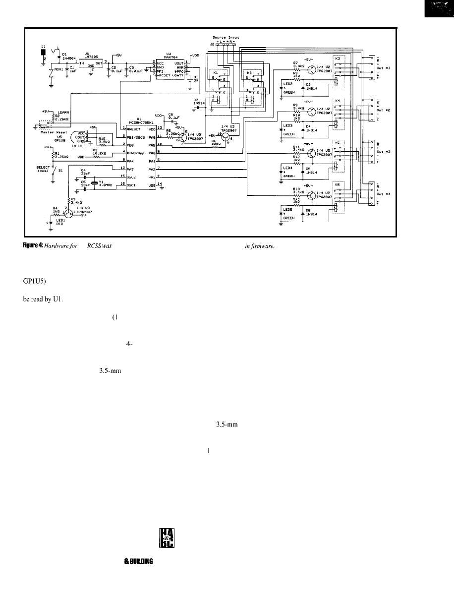
the
kept to an absolute minimum
by
performing most tasks
An infrared receiver/demodulator (Sharp
on the front panel filters and
demodulates the incoming infrared code to
The rear panel has spring-terminal
connectors for four speaker pairs 6
terminals). All connections from the rear
panel to the perfboard are made with
stranded 20-AWG wire. A rear-panel,
position, polarized interlocking connector
provides connection to the source amplifier.
Power is supplied through a
phone
jack on the rear panel. The case is black,
anodized, extruded aluminum with an
integrated card guide for the board.
OPERATION
The RCSS is operated with an IR
remote control. To use the RCSS, it must be
installed and programmed for the particular
system it is to be used with. Up to four
speaker sets may be connected. Speaker
wiring should be installed before the RCSS
is set up. The following sections address
installation, setup, and operation.
INSTALLATION
Before making any connections to the
RCSS, the lithium backup battery should be
installed. Although the backup battery is not
required for operation, it enables RAM data
retention when normal power is disrupted.
layout on the rear panel. The easiest way to
get the RCSS up and running is to first make
connections to the speaker sets and source
This means that the RCSS does not have to
amplifier on the rear panel, then position the
RCSS where it can receive infrared signals.
be reprogrammed after a power interruption.
Speaker sets are wired to the rear panel using
16 spring-release terminals. Red is positive
Refer to Figure 5 for the connection
and black is negative for the four sets of
terminals with the right channel located
along the top row. The source amplifier is
connected through the interlocking connec-
tor (Molex) with pigtails.
Virtually any common IR remote
control works. The idea is to pick four
front-panel red LED when it has not
buttons on a remote (or remotes) to
been programmed. The first step in
select among the four speaker set
outputs. In many cases, there are some
buttons on an existing remote control
setup is to decide which remote
that are unused or operate a compo-
control operates the RCSS.
nent not used in the your system.
An example of this might be a
receiver remote that includes buttons
for controlling a same-brand CD
player when the CD player owned is a
different brand. In this case, the CD
buttons can be used to operate the
RCSS from the receiver remote. You
could also purchase an inexpensive
replacement remote for TV or VCR or
use four buttons on a remote from a
remote-controlled component or TV
not being used. Again, most remotes
work. Just pick four buttons on any
remote.
Power is supplied through a wall
transformer. Plug the
phone plug
from the wall transformer into the power
jack on the RCSS rear panel, and plug the
transformer into a IO-VAC outlet. There is
no power switch so the RCSS normally
remains on. When power is connected for
the first time, the front-panel Learn indicator
(red) blinks. The RCSS is now installed and
ready for setup programming.
SETUP PROGRAMMING
Figure 5 shows the front panel
during the setup programming
discussion. The RCSS blinks the
To program the RCSS, push the
rear-panel Learn switch down. This
puts the RCSS into learn mode
(indicated by the steady illumination
of the red LED on the front panel).
80
APRIL 1995 HOME AUTOMATION
CONTROL
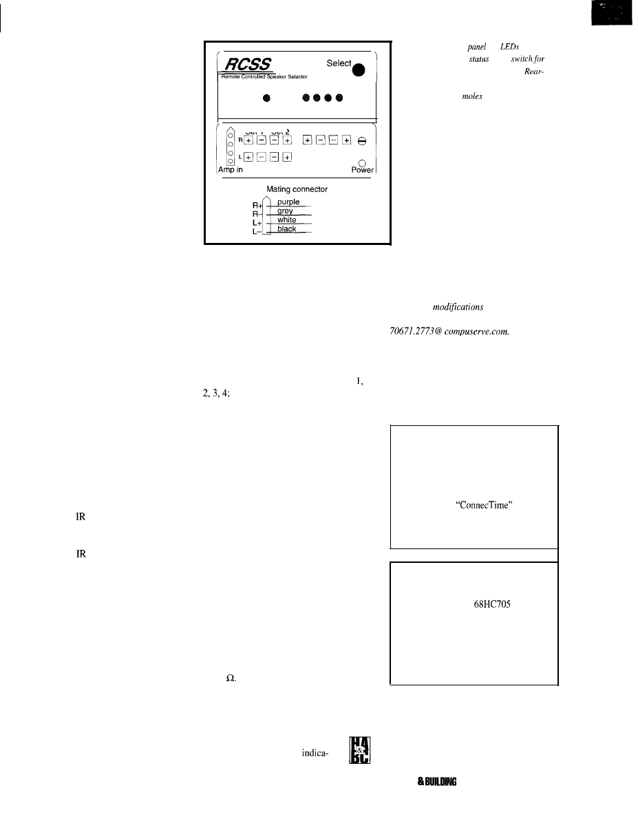
Stand several feet away from the unit,
point the remote control at the unit,
and push and release the four buttons
on the remote corresponding to each
speaker set in sequence 1, 2, 3, and 4.
Each time a button is pressed, the
green
LED corresponding to the next
speaker set to be programmed
illuminates. When all four buttons
have been pressed, all front-panel
indicators go out. When the red Learn
indicator turns out, the unit is in
recognize mode. When all green
indicators turn off, no speaker sets are
selected. By pressing any of the four
buttons just programmed, the RCSS
selects the corresponding speaker set
output. The RCSS will not respond to
other IR remotes or buttons.
Note that programming the
RCSS must be done under optically
quiet conditions. This means that any
IR repeaters should be covered or
otherwise disabled and no other IR
remotes are in use. Also, during
programming, if the remote buttons
are held down too long, then several
speaker sets will be programmed to
the same remote button. If this
happens, simply reprogram the RCSS
by depressing the rear-panel Learn
switch and pressing the appropriate
remote-control buttons again.
USING THE RCSS
When the RCSS has been
programmed, it is ready for use. The
RCSS works with commonly
available
remote repeater sets.
These sets usually have a transmitter
and receiver. They convert the remote
control’s
signals to an RF signal,
transmit them to a receiver, which
then converts the signal back to IR to
control the component.
Some repeaters are hard wired.
But, regardless of the technology
used, the result is the same. A repeater
can be placed in any room where
secondary speakers are located,
enabling remote-control selection of
that set of speakers from that room.
When a particular set of speakers
is selected by remote control, a
confirmation tone is sent to the
speaker set. This confirms that the
correct selection was made since the
user typically cannot view the front-
Speaker set
Learn
1 2 3 4
Set
1 Set
2
Set 3 Set 4
Learn
q
EIEIO
to amplifier
panel indicators on the RCSS. Each time the
selection is made by remote, a confirmation
tone is sent.
The Select button on the front panel
enables a local speaker-set selection. Each
time Select is pressed, another speaker set is
selected as indicated by the front-panel
indicators. The Select button also enables the
user to select any two speaker sets at once.
The Select button follows this sequence:
1 and 2; 2 and 3; 3 and 4; 1 and 3; 2
and 4; 1 and 4. The pattern then repeats.
There is no confirmation tone when Select is
used to select speaker sets.
The infrared detector in the RCSS is
quite sensitive and is typically able to read
infrared codes from 30’ or more. This means
remotes or IR repeaters can be conveniently
and aesthetically located. The only require-
ment is that there must be a clear line of
sight from the repeater receiver to the RCSS
IR detector on the front panel.
CONCLUSION
The RCSS switches four speaker pairs
from one stereo source by recognizing
unique IR codes from common IR remote
controls. Combining the RCSS with an IR
repeater enables remote-controlled speaker
selection from any location within the
repeaters range.
Relay-switching capacity during audio
peaks is 5 A, which corresponds to 200 W
into 8
The peak current capacity of closed
contacts is much higher, so virtually any
power level can be accommodated with no
interference to sound quality (low-resistance
contacts).
The unit has optional front-
panel manual controls and
Figure 5: The front
has
for
speaker
selection and learn
and a
manual selection
of
speaker
pair(s).
panel push terminals
are for
speaker
connection and a
connector is for the
source amplifier. The switch is a momentary,
center-off switch. Down invokes the learn
mode and up resets the microcontroller.
tors and an internal tone-signal genera-
tion to provide user feedback of
successful remote switching. A very
efficient code-recognition algorithm
means a small and inexpensive
microcontroller can be used. No exotic
parts are necessary for construction, so
cost is reasonable.
Scott
Heiserman
holds an MS in electrical
engineering. He currently develops analog
and digital
and embedded
solutions for the FAA. He may be reached at
Clark Oden holds a BS in electrical
engineering and designs precision time and
frequency equipment. He also works with
RF, analog, hardware, and software for FAA
applications.
SOFTWARE
Software for this article is available
from the Circuit Cellar BBS and on
Software On Disk for this issue. Please
see the end of
in this
issue for downloading and ordering
information.
SOURCE
A preprogrammed
may be
ordered for $25 postpaid from:
RCSS Project
10104 St. Helens Dr.
Yukon, OK 73099
I R S
422
Very Useful
423
Moderately Useful
424 Not Useful
HOME AUTOMATION
CONTROL APRIL 1995
81
DEPARTMENTS
Firmware Furnace
From the Bench
Silicon Update
Embedded
Ed Nisley
Journey to the Protected Land:
With Interrupts,
is Everything
n my time line,
it’s mid-December
and the Pentium FPU
‘firestorm threatens to
consume Intel’s credibility, if not their
future. On your time line, it’s late
March and you know how the story
ends. All I can say now is that I’m glad
for my plain old
Sometimes
the thick edge of the wedge is the
place to be!
Just as all programs have bugs, all
hardware has quirks. If you never
stumble upon the circumstances that
trigger a quirk, its presence doesn’t
matter to you. Knowing that a quirk
exists can either help you avoid it or
justify buying something else. That
may explain why it’s so difficult to get
errata lists-if a bug isn’t mentioned,
does it really exist?
This month, we’ll reinforce the
error handlers that catch our own
bugs, then measure a hardware
interrupt’s response time when it
triggers a task switch. The venerable
8259 Programmable Interrupt Control-
ler and all its LSI progeny have an
interesting, well-documented quirk
that most folks have never encoun-
tered; you’ll get the story here!
IN CASE OF EMERGENCY...
Ever since we first flipped into
bit protected mode, a simple error
handler has watched for protection
82
Issue
April 1995
Circuit Cellar INK
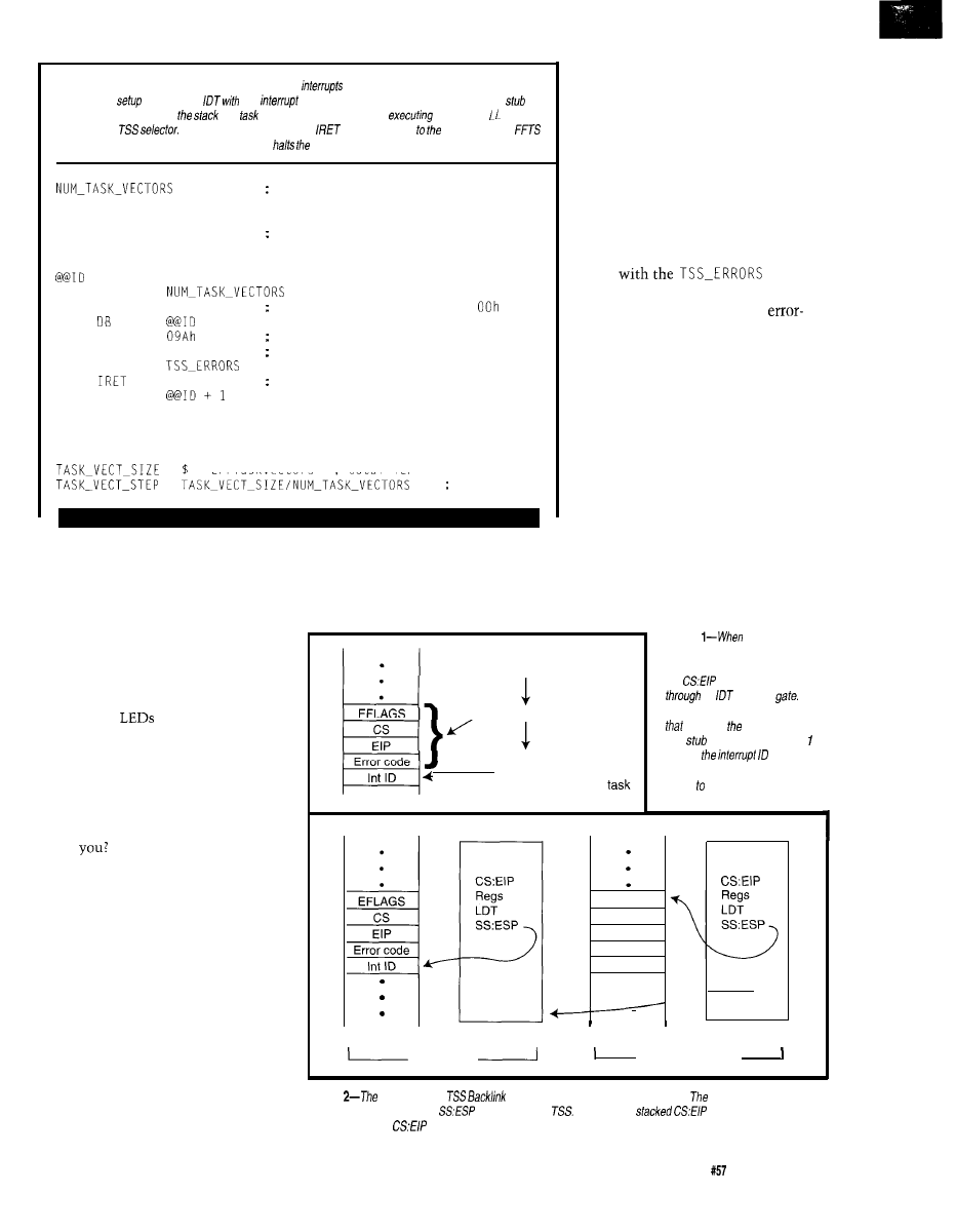
Listing
l--The unexpected error handler deals with
that are not caught by any other handler. The
error handler
code fills the
256
gates aimed at these 256 stub routines. Each
pushes the Interrupt ID on
and
switches info the handler by
a FAR CA
containing its
Although fhe stubs include an
fo return control failing fask, the
error handler simply displays an error dump and
system.
= 256
all possible interrupts
CODESEG
ALIGN 2
get a nice offset
PROC
ErrTaskVectors
=
0
REPT
DB
06Ah
PUSH immediate byte, MSB =
DB
FAR CALL with imm seg:offset
DD
0
offset is not used here
DW
;
seg
causes task switch
return from interrupt (ha!)
@@ID =
ENDM
ENDP
ErrTaskVectors
= ErrTaskVectors
total length of all stubs
=
stub size
violations. Without the support of the
CPU’s multitasking hardware, how-
ever, it’s difficult to write an error
handler that doesn’t mess things up
while attempting to display an error
message.
As a result, the only indication of
an error was a cryptic pattern on the
Firmware Development Board and
parallel port
identifying the
failing instruction. While that may be
better than real-mode pinball panic or
a system freeze, we can do much
better using separate tasks for the error
handlers. You knew multitasking was
going to come in handy for something,
didn’t
Figure 1 shows the sequence of
events after the CPU detects an error
in protected mode while running a
task. If the IDT entry corresponding to
that error contains an interrupt or trap
gate (the other choice is a task gate,
which we’ll discuss shortly), the CPU
pushes the current EFLAGS, CS, and
EIP registers onto the stack. Some
errors also produce an error code to
help identify the problem, which the
CPU pushes atop EIP, rendering a
simple I RET impossible. Figure 3 in
INK 50
tabulates the predefined
interrupts, their types, and whether
they produce an error code. (Note that
there is a table of acronyms at the end
of the article for those who didn’t
quite follow the past few sentences.)
Failing instruction
, Interrupt gate
The interrupt or trap gate directs
the CPU to a stub routine that pushes
the interrupt ID number. Without that
value on the stack, the handler cannot
tell which interrupt activated it. The
alternative is 256 separate interrupt
handlers, which seems excessive even
to me. Listing 1 shows the macro that
generates 256 stubs leading to our new
error handler.
Each stub includes a synthetic FAR
CALL
selectorin
the segment position. That selector
corresponds to the TSS of the
handler task. The CPU reacts to this
FAR CALL by storing the failed task’s
state in its TSS and task switching to
the error handler. As always, the CPU
loads a new state from the incoming
TSS, ensuring that all the registers are
safe from harm and the new stack is
entirely separate from the old one.
If you thought task switching was
complex last month, hold onto your
keyboards. Figure 2 shows the situa-
tion just after the task switch. The
stub’s FAR CALL triggers two new
actions during the task switch: the
CPU stores the failed task’s TSS
selector in the error handler’s TSS
Stub code
PUSH Int ID
CALL Error Handler
Figure
an error occurs in
a protected-mode instruction the
CPU pushes the current flags and
fhe
registers before passing
an
interrupt
Some
errors also generate an error code
identifies failing segment.
The
code shown in Listing
pushes
and
executes a FAR CALL task
switch the error handler.
Stack
TSS
Failing task
Error Handler task
Back Link
TSS
Figure
error handler’s
field holds the failed task’s
JSS
selector.
error handler accesses
fhe stacked values using the
values from that
Note that the
points to the failed
instruction and the
in the TSS points to the instruction after the FAR CA L L in fhe stub routine.
Circuit Cellar INK
Issue
April 1995
83
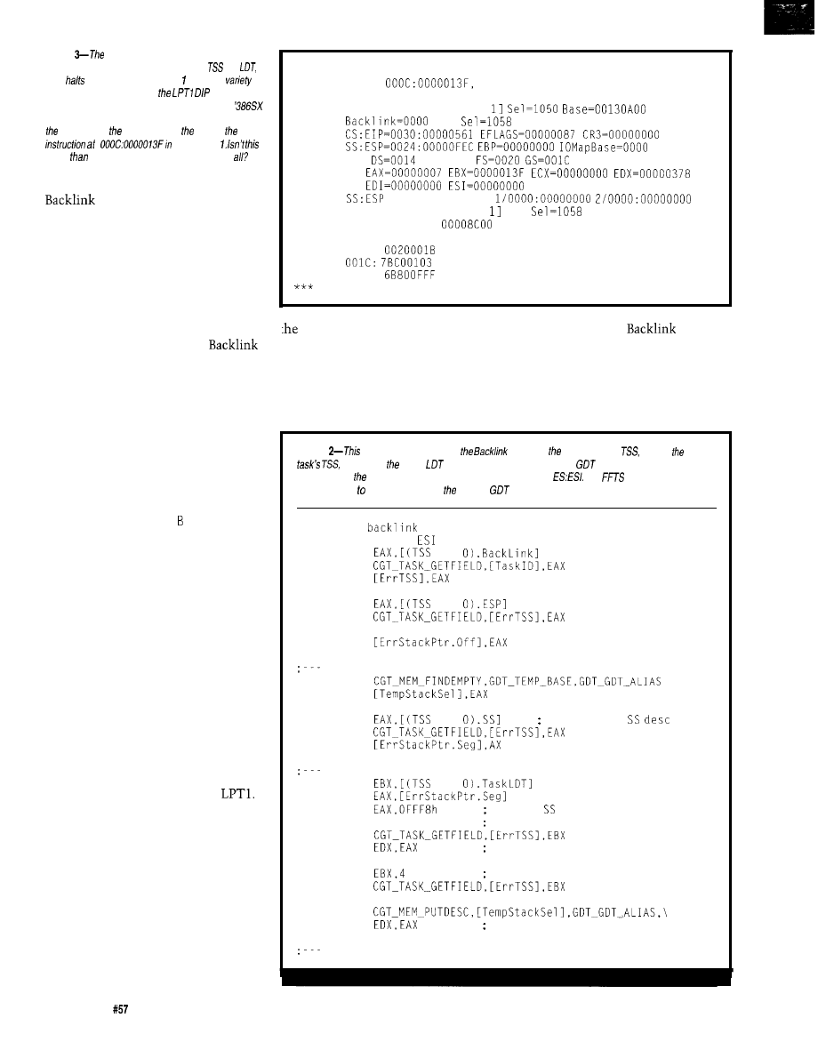
Figure
error handler displays values from fhe
failed task’s stack, dumps fields from ifs
and
then
fhe system. Demo Task causes a
of
(deliberate!) errors based on
switches.
This dump occurred after a floating-point op in a
system without a numeric coprocessor. As shown on
second line, CPU defected error in
Demo Task
better
pinball panic or no error indication at
field and sets the NT bit in
EFLAGS.
Unlike task switches through FAR
J M Ps, nested tasks can return to the
previous task using an I RET instruc-
tion. A normal I RET restores CS:EIP
and EFLAGS from the current task’s
stack. If the NT bit is set, however, the
CPU treats an I RET
as a
task switch
using the TSS selector in the
field. As we’ll see, this lets an inter-
rupt trigger a task switch, perform a
function in complete isolation from
the interrupted task, and return
directly without executing any special
code.
A more complex operating system
than FFTS might attempt to fix up the
condition causing the error and retry
the failing instruction. For example,
the CPU triggers I n t 0 (“Segment
Not Present”) when an instruction
uses a descriptor that is not present (P
bit = 0). The error handler can reach
back through the nested TSS, find the
offending descriptor, make it present
(perhaps by allocating a block of
memory and reading a code segment
from disk), then restart the failed
instruction. This is obviously not for
the faint of heart!
Our error handlers, on the con-
trary, display the values from the
failed task’s stack, dump fields from
its TSS and LDT, and halt the system.
Demo Task
1
can now cause a variety
of (deliberate!) errors depending on the
settings of the DIP switches on
Figure 3 shows a screen dump result-
ing from executing a floating-point op
without a coprocessor.
The second line in Figure 3 shows
the interrupt number and the address
of the instruction that caused the
problem. The CS:EIP values in the TSS
dump point to the FAR CALL instruc-
tion that switched into the error
handler. The remainder of the registers
have the same values they did when
84
Issue
April 1995
Circuit Cellar INK
*** Fatal error detected...
Int 07 at
flags 00010087, error code not used
Coprocessor not available
TSS Dump of [Demo Task
LDT
Trap=0000
ES=0000
O/OOOO:OOOOOOOO
LDT Dump of [Demo Task LDT
0004: 00302380
OOOC: 37300178 00409810
0014:
00409314
0040934A
0024:
0040934A
The system is stopped
error occurred. Reconstructing the
handler extracts the
field
problem is much easier when you can
from its own TSS to identify the failed
see what went wrong!
TSS. Next, it recovers the SS:ESP
Fetching data from the failing
registers in use at the time of the
task’s stack is a three-step process as
failure and copies the corresponding
shown in Listing 2. First, the error
stack descriptor to a temporary GDT
Listing
error handler code reads
field from error handler’s
locates failed
and copies task’s
stack descriptor info a temporary
descriptor. The error handler
can fhen copy task’s stacked values info local variables using
The
handler includes
additional code hand/e errors when kernel’s
stack descriptor is in use.
--- fetch
from our TSS to the task with the error
move ESP into
so we can read the stack
LEA
PTR
CallSys
MOV
LEA
CallSys
MOV
MOV
PTR
ESI,EAX
set up
CallSys
MOV
temp descriptor for stack
LEA
CallSys
MOV
PTR
get failing
copy stack descriptor from LDT to GDT
LEA
PTR
MOVZX
AND
convert descriptor to offset
ADD
EBX,EAX
add to LDT base offset
CallSys
MOV
save for later
ADD
fetch second dword from LDT
CallSys
CallSys
set temp descriptor to stack
fetch values from that stack and sort out error codes
(continued)
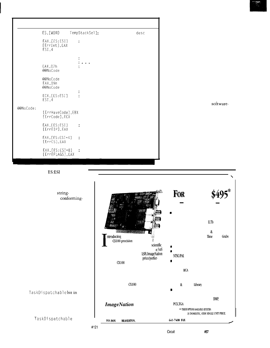
Listing Z-continued
MOV
PTR
aim ES at stack
MOV
MOV
ADD
interrupt number pushed by stub
XOR
XOR
CMP
JBE
CMP
JAE
CMP
JE
INC
MOV
ADD
EBX,EBX
assume no error code
ECX,ECX
zero if not used
decide if we have an error code
EAX,lOh
EBX
we
do, so flag it
and fetch it
MOV
MOV
MOV
MOV
fetch EIP
MOV
MOV
fetch CS
MOV
MOV
fetch EFLAGS
entry. Finally, with
aimed at
the stack, it can copy the values into
local variables.
The error handler produces the
output display using the
formatting routines in the
code segment we set up last month.
Those routines work with values from
the caller’s stack and do not affect any
other system values, making them
ideal for an error handler that may get
control at any time.
WHEN ALL ELSE FAILS...
The error handler is a task much
like the demo taskettes, except that it
runs only twice: once during the initial
task setup and once when an error
occurs. After displaying the error
information, it halts the system,
effectively eliminating the need to
unwind the stacks and return to the
failing task.
The
the dispatching array is set when the
task-initialization code creates the
error-handler task. After the handler
finishes preparing for the first error, it
turnsoffits
bit
and returns to the dispatcher, leaving
the context of the dispatching proce-
dure on its stack. The only way it will
regain control is through one of the
stub routines after an error, not
through the dispatcher’s loop.
When an error occurs, the CPU
restores the handler’s registers from its
TSS and the code finally returns from
the task-dispatcher procedure. It
should not call the dispatcher when it
finishes handling the error because the
dispatcher is not expecting a return
from a task it hasn’t dispatched.
The Intel System Software
Writer’s Guide
describes a moderately
complex way to integrate
and hardware-dispatched tasks. I have
not used their technique because the
FFTS error handlers are quite simple. If
you are building a system that must
recover from errors with a bit more
grace, pay attention to those sugges-
tions!
The handler I just described can
deal with all but three of the CPU’s
error conditions. The Intel manuals
recommend that stack, double-fault,
-P
RECISION
F
RAME
G
RABBER
the
video frame
grabber for OEM, industrial
and
applications. With sampling jitter of only
and video noise less than one
breaks new ground in imaging
mance. The
is a rugged, low power, ISA
board featuring rock solid, crystal controlled
timing and all digital video synchronization.
A
Software developers will appreciate the simple
software interface, extensive C library and clear
documentation. The
is a software com-
patible, drop-m replacement for our very
popular Cortex I frame grabber.
A
Call today
for complete specifications and volume pricing.
Corporation
Vision Requires Imagination
800-366-9131
O
NLY
CXlOO FEATURES
. Crystal Controlled Image Accuracy
Memory Mapped, Dual-Ported Video RAM
n
Programmable Offset and Gain
n
Input, Output and Overlay
n
Resolution of 5 12x486 or Four Images
of 256x243 (CCIR 512x512 256x256)
n
Monochrome, 8 Bit, Real
Frame
n
Graphics Overlay on Live or Still Images**
External Trigger Input
RGB or B&W, 30 Hz Interlaced Display
n
Auto Detect, Auto Switch
VCR and Resettable Camera Compatible
n
Power Down Capability
. BNC or
Connectors
n
Built-In Software Protection**
n
63 Function C Library with Source Code
l
Text Graphic
with Source Code
Windows DLL, Examples and Utilities
n
Software also available free on our BBS
n
Image File Formats: GIF, TIFF,
PIC,
and WPG
COST.
*
5495
276
OR
97075 USA PHONE (503)
(503) 643-2458 BBS (503) 626-7763
Cellar
INK
Issue
April 1995
85
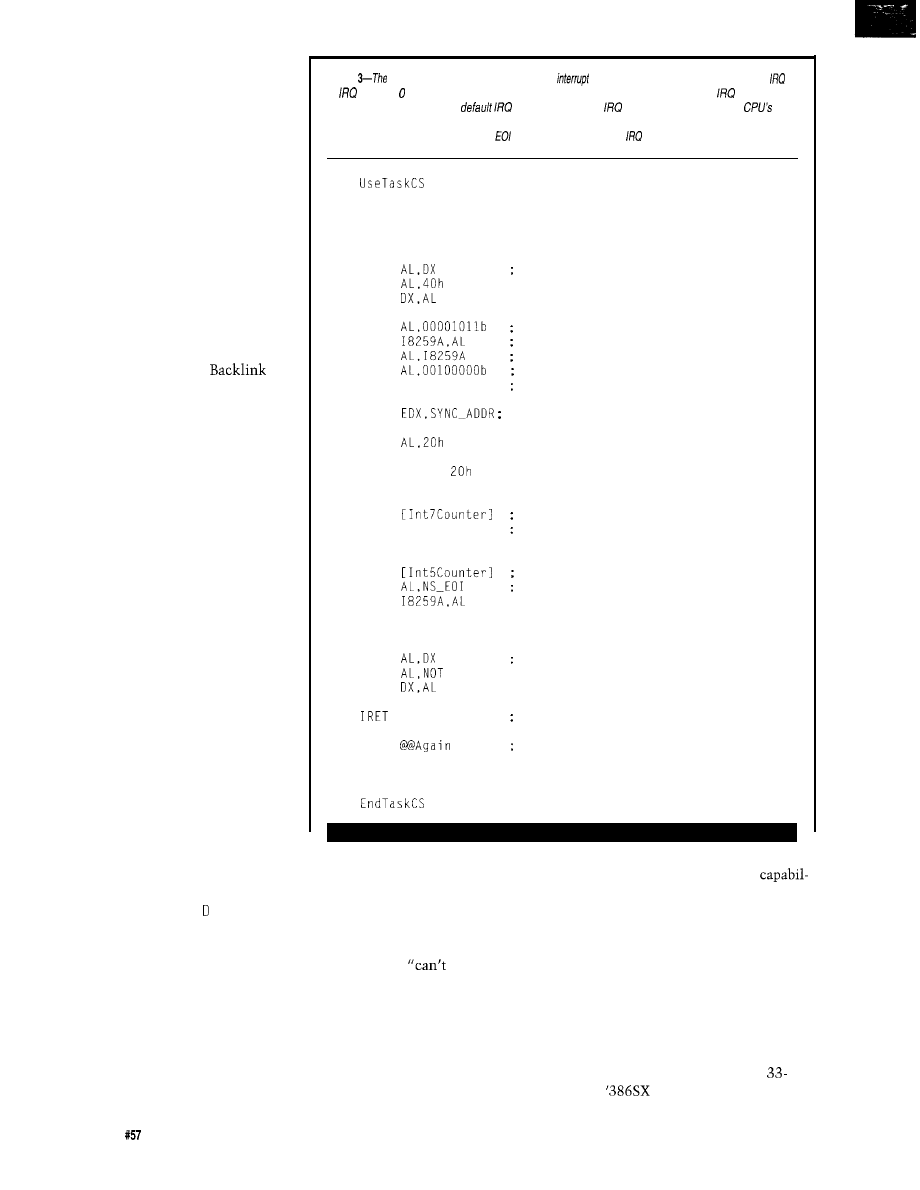
and invalid TSS error handlers use IDT
task gates rather than interrupt or trap
gates. In each of these cases, the
currently active stack may not be valid
or may not have enough room for the
error handler’s use. Any attempt to
push data onto a bad stack causes
further errors and may force the CPU
into shutdown.
Listing
system task-switches to this
handler whenever an interrupt occurs on either
5
or
7. Timer on the Firmware Development Board produces a 1-ms square wave on
5. The 8259
interrupt controller produces a
7 interrupt when the
5 input goes low during fhe
interrupt acknowledge sequence. The two cases are distinguishable by reading the 8259’s /n-Service
Register. The handler must not send an
to fhe 8259 when a default
7
occurs.
PROC TaskProcInt
A task gate is Yet Another
Descriptor that specifies a TSS selector
in place of the usual code-segment
selector. When an error occurs, the
CPU uses the corresponding IDT task
gate to switch tasks without pushing
any information on the failed task’s
stack, thus ensuring no further errors
occur. The error handler’s
field points to the failed task and the
handler may return using an I RET
after resolving the problem.
If the error condition produces an
error code, as is true for these three
errors, the CPU pushes it onto the
error handler’s stack. Because the task
switch occurs at the failing instruc-
tion, the TSS fields contain all of the
information required to locate the
problem. There is no need to find the
failed task’s stack and exhume values
from it.
Tasks activated by an IDT task
gate cannot use the FFTS task dis-
patcher because the CPU plops the
error code atop the stack contents
defined by the SS:ESP fields in the
handler’s TSS. This disturbs the
previous return context and results in
a protection error when the CPU
attempts to resume execution with a
“bad” stack. Not a pretty sight.
@@Again:
MOV
EDX,SYNC_ADDR
IN
raise the blip
OR
OUT
MOV
OCW3 with read ISR set
OUT
tell the 8259
IN
read the ISR
TEST
is IRQ 5 active?
JNZ @@Normal
yes, so do a normal interrupt
MOV
n o , mark a default interrupt
IN
AL,DX
OR
OUT
DX,AL
AND
AL,NOT
OUT
DX,AL
INC
no, we have a default IRQ 7
JMP @@Done
do not send EOI for this one
@@Normal:
INC
record a normal interrupt
MOV
send EOI to controller
OUT
@Done:
MOV
EDX,SYNC_ADDR
IN
lower the blip
AND
40h
OUT
return to previous task
JMP
and repeat!
ENDP TaskProcInt
I defined three separate tasks for
Int 08, Int OA, and Int OC that expect
to find an error code on their stacks.
The main error handler installs these
three task gates after preparing the rest
of the IDT interrupt gates. The task
dispatcher resets the Ta s k i s pa
t c
h
a b 1 e bit for these tasks when it
creates them, thus preventing any
execution except when an error occurs.
stacks and one task for the remaining
I plan to favor simplicity over
253 cases with stub routines to save
ity. Download the code and spend a
the interrupt ID. You may prefer a
while thinking it over-you’re sure to
separate task for each of the CPU error
find ways to improve it!
conditions, plus one more for all the
other cases that
happen here.”
Because a task gets control
Once again, remember that
immediately, you cannot aim multiple
writing comprehensive error handlers
task gates at the same TSS if you must
is exceedingly difficult. The code I’ve
know which interrupt caused the
described and implemented is barely
switch. That’s why FFTS has four error
the beginning of a real operating
handlers: three separate tasks for the
system’s features. Even though FFTS
three errors that may have corrupt
needs additional ruffles and flourishes,
If you think all this is too complex
for words, compare Figure 3 with the
results of a similar goof in real mode.
Maybe this protected-mode stuff is
worthwhile?
TICKING A TASK
In INK 50, we found that a
MHz
responds to an external
86
Issue
April 1995
Circuit Cellar INK
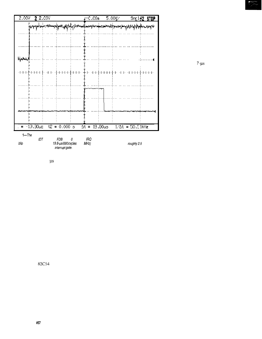
Photo
response to an external interrupt can be rather slow when the interrupt handler is a separate task
invoked through an
task gate.
Timer generates
5 on the top trace and the interrupt handler produces
the
on the lower trace. The
at 33
response time shown here is
times
longer than the delay through an
interrupt in about 7 when the
handler uses an IDT interrupt gate.
Now that we can set up and use
separate tasks, it’s reasonable to ask
what the response time for a complete
context switch might be. The CPU is
I modified Demo Task 2 to set up
obviously performing more work on
the machinery required to produce an
interrupt and then display the results
on the VGA. This gives you a real-time
our behalf while switching from one
view of what’s happening down at the
grubby hardware level. Because we’ve
task to another. So, how long does it
used protected-mode interrupts before,
I’ll skip the detailed listings and cover
take?
the new stuff.
Timer 0 in the Firmware Develop-
ment Board’s
chip produces a
1-ms square wave on the IRQ 5 ISA
bus line. The demo tasks require
several milliseconds to update the
VGA and LCD display and thus allow
several timer interrupts while they
are executing. If you don’t have an
FDB in your system, you can modify
the code to use the system-board
timer.
88
Issue
April 1995
Circuit Cellar INK
I remapped the system’s two 8259
interrupt controllers (or, more pre-
cisely, the LSI slivers that emulate
8259s) to produce Int 50-57 and Int
70-77 (hex), respectively. Because we
The interrupt handler shown in
are interested only in IRQ 5 on Int 55,
Listing 3 is a separate task that cannot
use the normal FFTS dispatcher
procedure. A task gate, much like the
I cleared just one bit in the primary
gates used for the CPU’s error han-
dlers, contains the IRQ 5 handler’s TSS
controller’s Interrupt Mask Register.
selector. When an IRQ 5 interrupt
occurs, the CPU reads the interrupt
All other external interrupts remain
number from the 8259, locates the
task gate in the IDT, and switches to
masked off.
the handler task.
After all the setup is complete, the
Demo Task 2 code executes an ST I
instruction to set the CPU’s IF and
enable external interrupts. Up to this
point, the FFTS kernel has been an
external-interrupt-free zone.
Photo 1 shows the results. The
rising edge on IRQ 5 in the top trace
triggers the interrupt. About 20 us
later, the second trace rises to show
that the interrupt handler is in control.
The ‘386SX CPU runs at 33 MHz, so
you are looking at about 650 clock
cycles of delay. A few microseconds
vanish while producing the output
pulse, but this is about as good as it
gets.
Dig out your back issues. Photo
1
in INK 50 shows a
response
through an interrupt gate (the cap-
tion’s “7 ms” is a typo). Photo 1 in
INK 54 shows that a task switch
requires about 15 us. It shouldn’t be
surprising that an interrupt plus a task
switch requires somewhat more time
than a task switch alone, but less than
both together.
Protected mode offers a variety of
ways to respond to interrupts.
YOU
can
use an interrupt gate for handlers that
perform relatively simple actions or
task gates that switch the entire CPU
context. You may also, of course,
perform your own task switch in
firmware at the risk of taking more
time to accomplish less while evading
the CPU’s hardware protection. Unlike
running code in real mode, you’ve got
choices for your handlers.
SWITCHED SUPPRESSION
During each task switch, the CPU
reloads all of its registers from a TSS.
Although we haven’t covered all the
implications yet, that means the
EFLAGS register is unique to each
task. Bit 9 of EFLAGS is more com-
monly known as IF (Interrupt Flag).
Get it?
The IRQ 5 handler produces the
upper trace of Photo 2. Although
Timer 0 runs continuously, interrupts
are enabled only when Demo Task 2 is
active, as shown in the lower trace.
External interrupts occurring while IF
is zero are not recognized, just as in
real mode.
Moral of the story: in a multitask-
ing system, you must enable interrupts
in every task if you want consistent
response times. If any task disables
interrupts, you will get gaps while
interrupts receive no attention at all.
Because user tasks should not
have that much influence over the
system’s operation, the two-bit I/O
Privilege Level in EFLAGS affects the
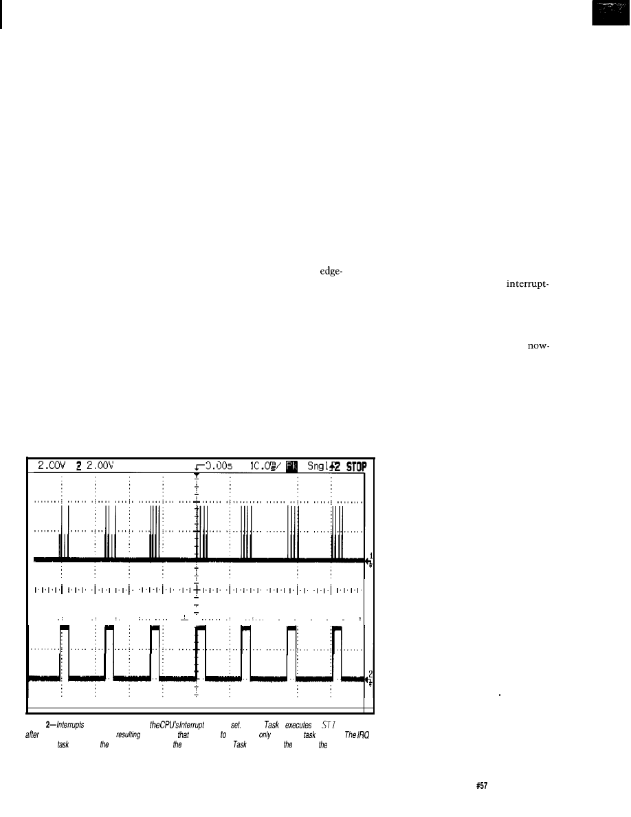
ST I and C L I instructions. If the
current task is less privileged than the
IOPL setting, the CPU invokes the
general-protection handler. This is an
effective way to prevent Level 3 user
tasks from clobbering the whole
system.
Normally, you change EFLAGS by
pushing it onto the stack, popping it
into EAX, altering a few bits, pushing
EAX onto the stack, and popping the
new value back into EFLAGS. In
protected mode, the CPU will not
change the IOPL field unless the task
is already running at Level 0, thus
preventing user tasks from changing
their own IOPL and gaining access to
sensitive system resources.
There are other complications that
we’ll explore in due time. For now,
just remember that interrupts are no
longer a private thing.
sheet:
CAP’N QUIRK TO THE BRIDGE!
You must cultivate the ability to
read hardware data sheets completely
and accurately if you intend to write
good firmware. It also helps if you can
read between the lines, because that’s
where the quirks are hidden. Consider
this excerpt from the Intel 8259 data
In both the edge- and level-
triggered modes, the IR inputs
must remain high until after the
falling edge of the first INTA. If
the IR input goes low before this
time, a DEFAULT IR7 will occur
when the CPU acknowledges the
interrupt.
Novices skip over this stuff
because it doesn’t make much sense.
An engineer with more experience
sticks a red Post-It note on the page
and scrawls timing diagrams in the
margin. The Perfect Master perceives
the implications without further
effort.
Me, I just sort of muddle along.
The Original PC used
triggered interrupts, creating compat-
ibility barnacles that force all ISA bus
systems into the same mode. EISA
systems may (and Micro Channel
systems always) use level-triggered
interrupts with cards built to share
interrupts. You can actually use level-
triggered interrupts in an ISA bus
system, although I’ll leave that as an
exercise for you.
line must have a rising edge, it must
There are three requirements for a
valid edge-triggered interrupt: the IRQ
Photo
are active only when
Flag is Demo
2
an instruction
preparing for interrupts,
in a system
responds interrupts
when that
is active.
5 handler produces clusters of pulses in fop trace. Demo
2 produces blips in lower trace
when if is active.
remain high until the CPU acknowl-
edges the interrupt, and (obviously) it
must go low to prepare for the next
interrupt. The 8259 holds its INT
output high whenever it has an
interrupt pending.
Contrary to popular assumption,
however, the 8259 does not “remem-
ber” an interrupt that Goes Away
before the CPU detects it, even in
edge-triggered mode. If the IRQ input
goes low, the 8259 lowers its INT
output. The CPU will not detect an
interrupt.
The data sheet description applies
only to IRQ inputs that Go Away in
the short interval when the 8259 is
processing the CPU’s first INTA pulse.
In that situation, the CPU detects a
pending interrupt, starts an
acknowledgment cycle, and then
suddenly discovers that it doesn’t have
a valid IRQ input. What to do?
You could argue that the 8259
should issue an interrupt for the
vanished IRQ. However, that could
cause system problems if the inter-
rupting hardware no longer needs
service. Worse, the interrupt could
have been a brief glitch on the line
rather than a valid signal.
What the 8259 actually does is
generate an IRQ 7 interrupt with ISR
bit 7 set to zero. Thus, the IRQ 7
interrupt handler must distinguish
between valid IRQ 7 hardware inter-
rupts and default interrupts. Invalid
timing on any interrupt line, including
IRQ 7, causes a default IRQ 7.
When the interrupt handler
detects a default IRQ 7 event, it must
not send an EOI command to the 8259.
An EOI resets the highest-priority ISR
bit and may discard a valid interrupt if
the 8259 recognizes a new IRQ signal
while the CPU is busy with the default
IRQ 7.
Because Timer 0 is not synchro-
nized with the CPU’s clock, we can be
sure that it will eventually violate the
(unspecified) timing specs causing a
default IRQ 7 interrupt. All we have to
do is sit back and watch..
Demo Task 2 installs task gates at
both Int 55 and Int 57 to invoke the
handler task in Listing 3. The handler
determines which interrupt invoked it
by reading the 8259’s ISR. If bit 5 is
Circuit Cellar INK
Issue
April 1995
89
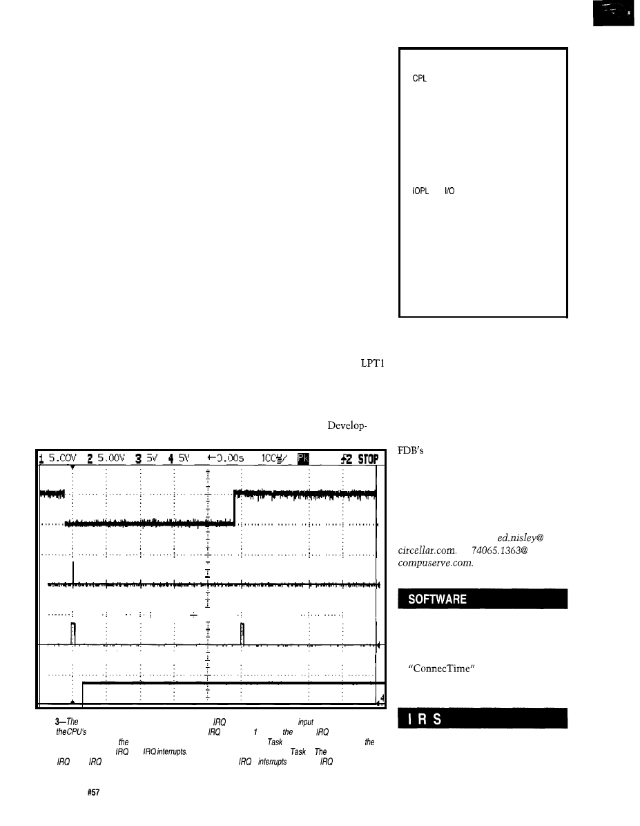
clear, meaning that a valid IRQ 5 did
not occur, then the interrupt must be a
default IRQ 7. The code pulses parallel
The main loop of Demo Task 2
port bits 6 and 5 to give us a real-time
displays the two interrupt counters
and their ratio, scaled by a factor of
picture of what’s happening.
one million, on the VGA display each
time it runs. The interrupt handler
task simply increments the counters
and returns because we don’t have
nearly enough time between interrupts
to update the screen.
Photo 3 catches a default IRQ 7 in
action. The bottom trace goes high
when Demo Task 2 is active. External
interrupts are enabled a few microsec-
onds before the rising edge of that
pulse when the CPU exits from the
task switch instruction. The Timer 0
pulse on IRQ 5 shown in the top trace
falls just before that key event.
The blip on Trace 2 marks a
default IRQ 7 interrupt. Trace 3 shows
two interrupt handler task activations:
first for the default interrupt and then
as a valid IRQ 5 after the rising edge of
Timer 0.
After about 64 hours of continu-
ous execution, the program recorded
68.3 million IRQ 5 and 11,815 default
IRQ 7 interrupts. That works out to
172 parts per million-infrequent
Don’t get too nervous about this
condition, though. It only occurs when
the interrupt source Goes Away
enough that you’d never see one if you
precisely when the CPU is acknowl-
weren’t looking directly at it.
edging the interrupt. If your interrupts
are enabled all the time and the pulse
stays high longer than the maximum
CPU response time, you’ll never see a
default IRQ 7.
In any case, build a test into your
IRQ 7 and IRQ 15 handlers just in
case you get a glitch. Always accumu-
late a counter, then examine it once in
a while. Who knows? You might see
a one part-per-million blip occasion-
ally!
RELEASE NOTES
The demo taskettes include test
code for the error and interrupt
handlers. Demo Task 1 monitors
and triggers a variety of (deliberate!)
errors to verify that the handler tasks
work correctly. Demo Task 2 installs
an interrupt handler task, activates
Timer 0 on the Firmware
Photo
8259 interrupt controller generates
a
default
7 if an interrupt request
becomes inactive
during
hardware response. The falling edge of
5 in Trace triggers default
7 shown in Trace
2 because if occurs just
as
CPU becomes enabled for interrupts in Demo
2. Trace 3 goes high when
system responds to either
5 or
Trace 4 shows the start of Demo
2.
interrupt handler
counts
5 and
7 events. In this system, there are about 170
7
per million
5 inferrupfs.
Acronyms
Current Privilege Level
DPL
Descriptor Privilege Level
EOI
End Of Interrupt (command)
FDB
Firmware Development Board
FFTS
Firmware Furnace Task Switcher
GDT
Global Descriptor Table
GDTR GDT Register
IDT
Interrupt Descriptor Table
IF
Interrupt Flag
Privilege Level
LDT
Local Descriptor Table
LDTR
LDT Register
NT
Nested Task
P bit
Present Bit (in a PM descriptor)
RF
Resume Flag
RPL
Requestor Privilege Level
TF
Trap Flag
TR
Task Register
TSS
Task State Segment
ment Board, counts the number of IRQ
5 and IRQ 7 interrupts, and displays
running totals on the system’s VGA.
Demo Task 3 simply ticks a count on
the VGA and graphic LCD panel.
Next month, we’ll fire up the
system board’s real-time clock inter-
rupts, twiddle a watchdog, read a serial
number, put some characters on the
character LCD, and look at
memory allocation.
q
Ed Nisley, as Nisley Micro Engineer-
ing, makes small computers do
amazing things. He’s also a member of
Circuit Cellar INK’s engineering staff.
You may reach him at
or
Software for this article is avail-
able from the Circuit Cellar BBS
and on Software On Disk for this
issue. Please see the end of
in this issue for
downloading and ordering
information.
425
Very Useful
426 Moderately Useful
427 Not Useful
90
Issue
April 1995
Circuit Cellar INK
Jeff Bachiochi
Vaporwear:
Revealing Your Humidity
probably
heard someone
comment about
from an ache or pain. What they are
actually feeling is the change in
humidity as their bones and joints
swell or shrink from a change in the
air’s moisture content. We live
somewhere between the extremes of a
desert’s lack of moisture and a sauna’s
abundance of it.
Take those muggy summer days
(please); they can be brutal. The air
seems so heavy. And, for good rea-
son-it actually is. Humid air is
saturated with water vapor. In this
gaseous state, the water heeds the
same rules as the other gases which
combine to make air.
The relationship between air’s
pressure, volume, and temperature are
defined in the Ideal Gas Law:
T
where is pressure, V is volume, T is
temperature, K
is
the gas constant
times the number of moles of gas.
other words, pressure and volume are
inversely proportional, whereas
temperature is proportional to both
pressure and volume.
Water is in a significant part of our
lives. It’s in our bodies, what we eat,
and the air we breathe. The moisture
content of air can be measured by
weighing all the water-vapor mol-
ecules with respect to other gas
molecules-not an easy task for
tweezers, a magnifying glass, and a
postage scale.
However, it can be calculated
from knowing the dew/frost point
(DFP) of the air. The DFP temperature
represents the temperature that the
water in the air becomes saturated and
condenses into water or ice. The
warm, moist air we exhale on a cool
morning is chilled to dew point and
instantly condenses into water
droplets or fog. Measuring the exact
temperature at which the condensa-
tion takes place lets the relative
humidity (RH) be calculated.
Humidity affects us on a personal
level within our own comfort zone. It
is important to note here that humid-
ity is just as important to other
activities that operate in severe
environments. Industrial furnaces or
upper atmospheric experiments pose
special problems to the measurement
of humidity and require specially
designed sensors and/or sampling
equipment.
But, let’s try to remain within our
comfort zone here for the remainder of
this discussion.
COMFORT ZONE
MEASUREMENTS
For most of us, while the outside
temperature varies within a range of
our artificial living environ-
ment stays within
Those of
us with base-board heat don’t have
much control over humidity. We
might keep a kettle of water on the
wood stove or run a humidifier to keep
a bit of humidity in the air, but in
general most of us don’t have a
hygrometer on the wall next to the
thermostat.
Before we added on to our cottage
here in New England, it was heated by
a hot-air system. This old system,
antiquated as it was, did have a
humidistat located within the central
air duct. Whenever hot air was moving
through the duct, a fine mist of water
vapor was introduced in an attempt to
control the humidity. never actually
felt the effects of the humidistat
92
Issue
April 1995
Circuit Cellar INK
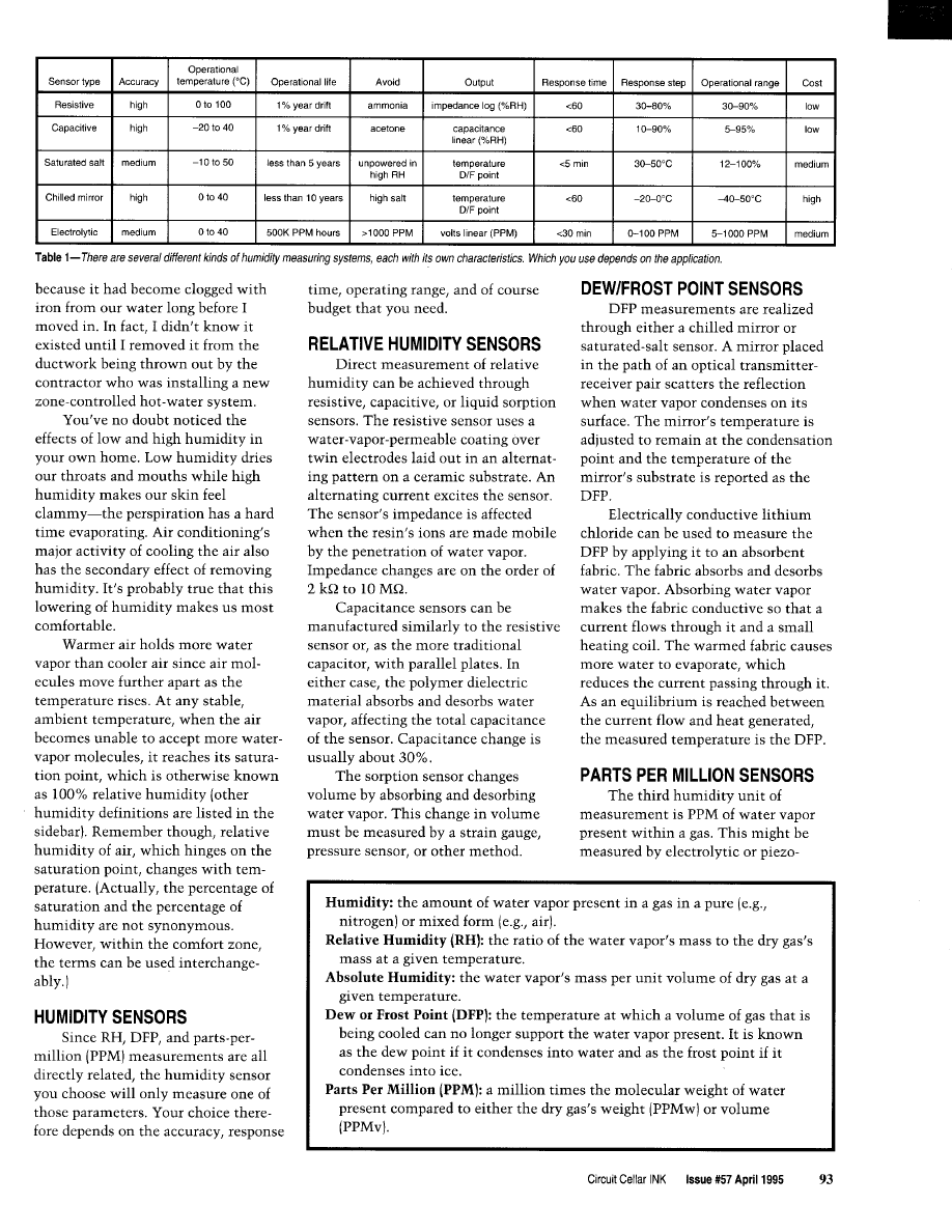
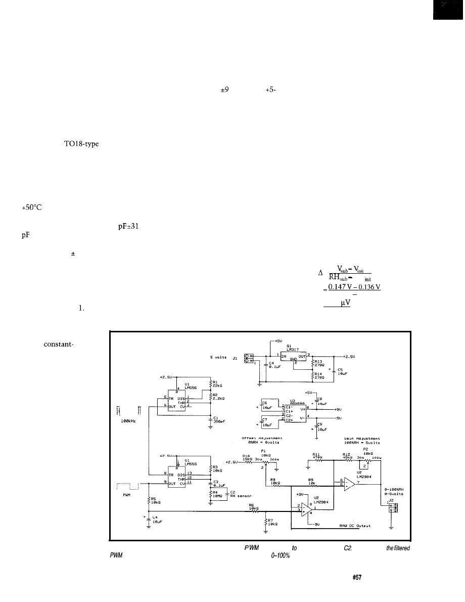
Still there are some firms willing
to make their sensor technology
available for a price, although it is by
no means small. Table 1 offers a
sample of available humidity sensor
characteristics.
IT’S ALL RELATIVE
Although I could have chosen a
offset stage to adjust 0% RH to 0 V and
a gain stage to allow 100% RH to be
measured as 5 V. The O-5-V signal can
be used directly by most A/D convert-
ers. The op-amp needs a bit of head
room on the power supply, so I used a
MAX680 to produce V from the
V circuit input.
number of different sensors, I will be
using Panametrics’ Humidicap-2. This
sensor is one of the smallest available.
It comes in a
can with the
top open to the atmosphere. A small
plastic sleeve prevents even the
clumsiest enthusiast from harming the
delicate wire bonds to the sensor.
Although physically delicate, the
sensor is rated to operate from -40 to
with negligible temperature
dependence above freezing. Bulk
capacitance at 33% RH is 207
(15%). Capacitance change from 10
to 90% RH is typically 12% of bulk.
The linearity is 1% over that range,
which means no algorithm is neces-
sary to correct for nonlinearities.
Calibration techniques usually
call for special salt solutions to create
accurate humidity levels in closed
containers. The sensor is inserted into
the chambers and allowed to stabilize.
Each salt solution maintains a particu-
lar humidity level. The circuit mea-
surements taken in two humidity
environments indicate the slope of the
sensor’s output in relation to the
humidity level.
My humidity chamber consists of
the upstairs bathroom with a portable
humidifier. Prior to taking the first
reading I let the sensor, circuitry,
hygrometer, and humidifier stand for
an hour to let all the apparatus get
climatized to the present environment.
An initial measurement shows 0.136 V
for a humidity level of 15%. After
three hours with the humidifier on, a
second measurement shows 0.147 V
for a humidity level of 70%.
Figure 1 shows a basic circuit for
converting capacitance to pulse width
and voltage. The actual board is
pictured in Photo Here, a MAX7556
(a low-voltage version of the dual 555
timer) is used. The first
stage is connected to
form a
frequency pulse genera-
tor. The second stage,
triggered from the first,
creates a varying pulse
width proportional to its
RC time constant.
Since the resistance
is fixed, the change in
To reduce the calibration costs to
a reasonable level, I was prepared to
create my own humidity chamber
once I had a way to measure it. On a
trip to the local hardware store, I
browsed the thermometer section.
With a couple of thermometers, I
could rig up a Sling Psychrometer and
measure wet- versus dry-bulb tempera-
ture differences and thus relative
humidity. Then, I noticed the combi-
nation thermometer/hygrometers.
They ranged in price from $4.99 to
Obviously, the voltage readings
can be used to calculate a percentage
of humidity. Assuming linearity, we
can calculate the sensor’s output for
the extremes of 0% RH and 100% RH.
To do this, we first of all have to find
the slope of the line between the
initial and subsequent voltage read-
ings:
=
RH
70% 15%
0.2
RH%
capacitance is directly
proportional to the pulse
width. This pulse width
could be measured
digitally through a
microprocessor’s timer
input and converted to
the corresponding
humidity level. Alter-
natively, the PWM
signal can be fed into a
low-pass filter and
measured as a voltage.
I used an additional
dual op-amp for an
Figure 1-A stable oscillator triggers a one-shot circuit where
is proportional the humidity sensor,
A voltage from
is offset and multiplied to approximate a C-5-V output equivalent to
relative humidity.
$32.95. After comparing the humidity
readings and display scales, I found the
least expensive and most expensive
models to be comparable.
Circuit Cellar
INK
Issue
April 1995
9 5
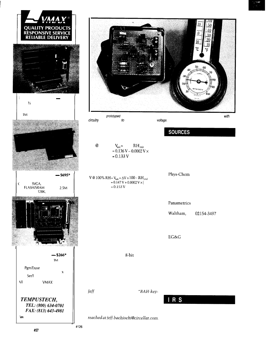
SOLID STATE DISK
$135”
Card 2 Disk Emulator
EPROM, FLASH and/or SRAM
Program/Erase FLASH On-Board
Total, Either Drive Bootable
25MHZ 386DX CPU
Compact AT/Bus or Stand Alone
In-Board
IDE, FDC, 2 Ser/Bi-Par
Drives to
Cache to
DRAM to 48M
TURBO XT
w/FLASH DISK
To 2 FLASH Drives,
Total
DRAM to 2M
FLASH On-Board
CMOS Surface Mount, 4.2” 6.7”
2
Par, Watchdog Timer
Tempustech
products are
PC Bus Compatible. Made in the
J.S.A., 30 Day Money Back Guarantee
‘QTY 1, Qty breaks start at 5 pieces.
INC.
for
295 Airport Road
ast
response!
Naples, FL 33942
96
Issue
April 1995
Circuit Cellar INK
Photo l--The
circuit is mounted on perf board for easy experimentation. The Humidicap sensor
this
enables humidify be read as pulse width or
With the slope of the line, we can
now find the voltage at 0% RH:
V 0% RH =
AV x
15%
and the voltage at 100% RH:
100-70)
Knowing the voltage readings at 0
and 100% RH, we are able to set the
op-amp’s offset and gain. For the offset,
apply the voltage calculated at 0% RH
to the input of the op-amp and adjust
the offset to 0 V out. Similarly, for the
gain, apply the voltage calculated at
100% RH to the input and adjust the
gain to 5 V out. Since these adjust-
ments interact, they should be done
more than once.
Even though an
ADC may
not seem like overkill in this case, the
O-5-V input converts the percentage of
RH at about 0.2% RH per bit, an
amount which no one will even
notice.
q
Bachiochi (pronounced
AH-key”) is an electrical engineer on
Circuit Cellar INK’s engineering
staff.
His background includes product
design and manufacturing. He may be
Relative humidity products:
General Eastern Instruments
High Voltage Engineering Division
20 Commerce Way
Woburn, MA 0 180 1
(617) 938-7070
Scientific Corp.
36 West 20th St.
New York, NY 10011
(212) 924-2070
Fax: (212) 243-7352
221 Crescent St.
MA
(800) 833-9438
Humidity transmitters and
moisture analyzers:
Environmental Equipment
217 Middlesex Tpk.
Burlington, MA 01803
(617) 270-9100
Humidity, temperature, barometric
pressure instruments:
Rotronic Instrument Corp.
7 High St., Ste. 207
Huntington, NY 11743
(516) 427-3994
428
Very Useful
429 Moderately Useful
430 Not Useful
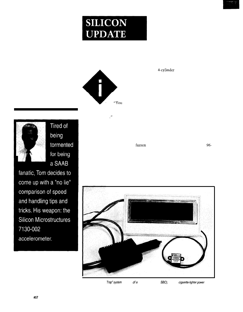
A Saab
Story
Tom Cantrell
Whether it’s the flight-deck
interior (Saab makes well-respected
commercial and military aircraft), the
stubborn reliance on front-wheel drive
and
turbocharged engines,
or quirky mysteries like why the
ignition key is between the front seats,
Saabs have a unique personality.
once
read a
That’s rare in these days of look-alike
review in a car
jelly beans when all cars seem to be
magazine that opened
designed by the same computer.
with
know those
There’s no denying I’m a
Saabaholic. I got hooked in 1983 and
corrupted my wife with a 1986 model.
In fact, I’m a card carrying member of
the local Saab club (Saabs Anony-
mous?). The club’s monthly meetings
are a good chance to shoot the breeze
and swap stories with fellow travelers.
Everyone claims their new setup,
whether a hot box, sticky tires, or
octane fuel, is just the ticket.
Saab owners, the ones who go to
foreign movies and build airplanes in
their basement.. Ho, ho, ho.
The pundits use the same “Saab
Story” title as an oh-so-clever way to
get in a few digs-perhaps a story
about a breakdown in the boonies and
an encounter with a grizzled pump
jockey. Claims he can fix “them
jobs” are rendered suspect by his
struggle with the hood (it flips forward)
followed by his pronouncement,
“You’ve got big troubles, my boy, the
motor’s in backwards.” Ho, ho, ho.
Yes, Saabs are weird-and that’s
exactly why I like them. What other
A Tale of
Speed and
Acceleration
car company introduces a model like
the venerable 900 and leaves it largely
unchanged for more than a decade!
Heck, everyone knows the thing to do
is fiddle with the styling, change the
name every couple of years, keep those
showrooms hopping.
This automotive equivalent of fish
stories brings us to the silicon part of
this story. My goal was to come up
with an instrumentation setup which
gives “no lie” comparisons of speed
and handling tips and tricks. Photo
1
Photo l-The “Speed
consists
data logger (LCD t
modified
supply
and an accelerometer.
9 8
Issue
April 1995
Circuit Cellar INK
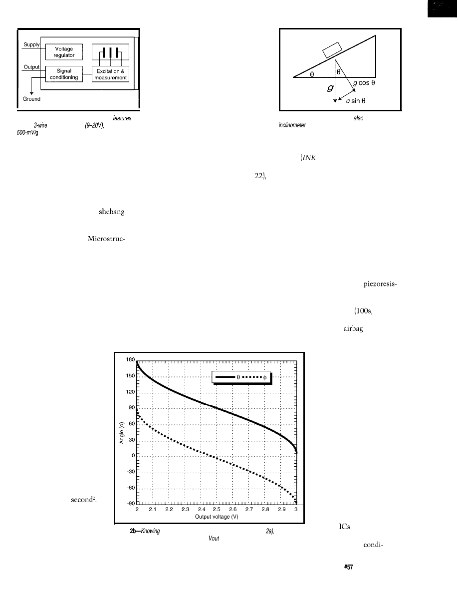
Figure l--The
Silicon
Microstructures
7130
a
simple
interface: power
ground, and a
output.
shows the resulting and aptly named
“Speed Trap” system. It consists of an
LCD display and small SBC (in the box
with the LCD) driven by one of those
cigarette lighter DC power supplies (I
modified the 4.5-V switch setting to
produce 5 V by changing a resistor).
The key to the whole
is a
gadget known as an
accelerometer
(the
small black cube], specifically the
7130-002 from Silicon
tures. Before hitting the road, let’s
check under the 7130’s hood.
NEWTON NABBER
An accelerometer measures that
Accelerometers work on the same
F = MA principle (i.e., a mass subject
to an acceleration generates-thanks
to inertia-a deflection force). By
knowing the mass and measuring the
force, acceleration can be determined.
Modern solid-state designs exploit
silicon IC process techniques to
micromachine tiny pendulums-truly
amazing stuff! However, there are
different techniques for measuring the
deflection force that lead to a variety
of subtle operational differences.
The simplest devices are piezo-
electronic. Long-time readers may
remember my article “Kynar to the
Rescue” about piezo sensors (INK
which covers the wondrous properties
of piezo material, best described as the
molecular equivalent of a motor or
generator. Like a motor, it can trans-
form electrical input into physical
work (e.g., piezo tweeters and our
beloved quartz crystals). Of relevance
in the current discussion, piezo
materials also generate electrical
output from work input, much as a
motor can act as a generator.
the inherent weakness of a simple
piezoelectronic design-it can’t handle
DC (i.e., constant acceleration). For
instance, you may remember the
ACH04 from AMP (interestingly, they
acquired the technology from the
Perhaps you’ve already guessed
0
g sin
Figure Pa-An accelerometer can
be used as an
if you apply some trigonometric
relationships.
Kynar folks) I mentioned in another
article
49). A close look at the
data sheet shows that the output is
only guaranteed down to 25 Hz.
tive units usually offer low sensitivity
To achieve DC frequency re-
sponse, a variation on the theme is
(i.e., millivolts or microvolts per g),
piezoresistive designs, which connect
the mass to the package with the
limiting them to high-g
1000s)
equivalent of strain gauges. However,
there are a couple of problems to
watch out for including temperature
sensitivity (i.e., a thermistor) and the
shock detection. That’s fine for
fact that external package-mounting
forces tend to migrate inside and bias
the response. Furthermore, though
applications such as
sensors, but
there are some exceptions,
definitely overkill for my test-drive
gravity exists and where it
mysterious force called
gravity,
came from even as many of
Newton’s concepts have
been replaced by relativity
understanding of which came to Sir
on a cosmic scale. Never-
theless, at earthly veloci-
Isaac Newton (probably along with a
ties, the old F = MA (Force
= Mass x Acceleration) still
works fine for reality
headache) in an errant, apple-induced
checking car enthusiasts’
hypes and hopes.
epiphany.
Philosophers still debate why
plans.
Enter the latest
technology-variable
capacitance-of which the
Silicon Microstructures
unit is an example. These
designs consist of a sus-
pended mass and plate,
with the gap between them
changed by deflection of the
mass-varying capacitance
(see Photo 2).
Despite the common
saying, gravity is an
acceleration rather than a
force. The unit of accelera-
tion is known as g which,
on Earth, happens to be
about 32 feet per
In other words, an object in
free fall travels at 32 feet
per second after one second,
64 feet per second after two
seconds, and so on.
Figure
the effect of gravity on an inclined object
(Figure
the angle of
incline is easily determined as a function of
for both horizontal (upper curve) and
vertical (lower curve) mounting.
The main claim to
fame for variable-capaci-
tance units like the 7130 is
high sensitivity. As shown
in Photo 3 and Figure l’s
block diagram, the unit
combines a micromachined
variable capacitor with
support
(i.e., voltage
regulator, calibration
memory, signal
Circuit Cellar INK
Issue
April 1995
9 9
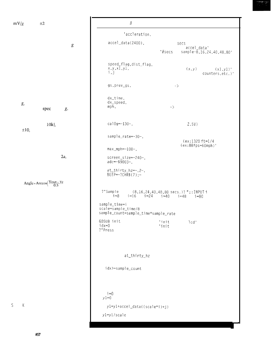
tioner, etc.) to deliver a whopping 500
across a g range. The inter-
face is blessedly simple, consisting of
power (it’s not fussy-anything within
9-20 V will do) and an output that
varies from 1.5 to 3.5 V, with 0
centered at 2.5 V.
The high-level output enables the
logger to capture meaningful data,
even with a lowly 8-bit O-5-V A/D
converter. You might think more bits
or some amplification
(to
expand the
2-V 7130 full-scale output to the A/D
converter’s S-V range) is called for, but
in fact it works fine as is. The 8-bit A/
D converter resolves down to about
0.04 which is a good match with the
7130’s accuracy
of 0.03
This high-tech wizardry comes at
a price-$225 for singles. However, in
high volume [e.g.,
the chip [along
with
50, 100, and 300 g cousins)
approaches a more reasonable $50.
As an aside, note that an acceler-
ometer that handles DC can work as
an inclinometer in certain applica-
tions. As shown in Figure the
acceleration vectors, acting on an
inclined 7130, are easily derived with a
little trig:
+ 1)
where the angle and output of the arc
cosine function are in degrees, and Vr
is either 2.5 V or 3 V depending on
whether the unit is mounted horizon-
tally or vertically (i.e. 1 g or 0 g at
rest-see Figure 2b).
The main restriction is that an
accelerometer is only useful as an
inclinometer when stationary-lest
real acceleration get mixed in with the
incline component. However, an
accelerometer-based solution is ideal
for harsh environments (i.e., shock or
temperature extremes) in comparison
to traditional floating-ball inclinom-
eters.
AUTOMOTIVE BASICS
Listing 1 shows the main part of
DRAG.
B DT that runs the Speed Trap
system. There is a second program,
H 0 . B DT, but it’s largely the same as
the first part of DRAG (i.e., it captures
the accelerometer data and graphs the
g curve) and is thus not shown.
100
Issue
April 1995
Circuit Cellar INK
Listing l-The D RA G . D T program records and displays acceleration, speed, and distance.
PROGRAM drag
speed, distance'
INTEGER
idx,
sample-time,
sample-count,
scale,
REAL
volts,
speed,prev_speed,
zero_to_sx,
dist.
t
CONST
offset=-114-.
gain=-8-,
dx=-660-,
sx=-88-,
'max 80
at 30 hz'
'index into
to
'#samples to take'
'#samples per pixel scale factor'
'flag O-speed, distance times'
'line start
and end
'int temp (for/next
'a/d reading'
'volts g'
'velocity in fps'
'O-to-speed time'
'time to distance'
'speed at distance'
'fps mph'
'distance traveled'
'temp'
'Og (virtual
calibration'
'centering factor'
'amplification factor'
'30 Hz'
'0-dx feet
mile)'
'0-sx fps
'to scale vertical axis'
'240 horiz. pixels'
'a/d converter port addr'
samples=-l-,
'name for sampling task'
'name for 30 Hz constant'
'ring PC bell'
BEGIN 'drag'
DO
time
UNTIL
OR
OR
OR
OR
OR
'compute #samples/pixel'
'compute #samples'
a/d and
pointer to log data'
a key to start logging...";
i=KEY
DO
i=KEY
UNTIL i<>O
RUN samples
BEEP
'dispatch sampler'
idle:
'and wait until done'
IF
then GOT0 ahead
GOT0 idle
ahead:
BEEP
all samples taken'
CANCEL samples
x=7
'so stop sampler task'
'start g curve at 8th dot'
FOR
TO screen-size-l
'for each pixel'
FOR j=O TO scale-l
'for each sample within pixel'
NEXT j
'compute average accel'
(continued)
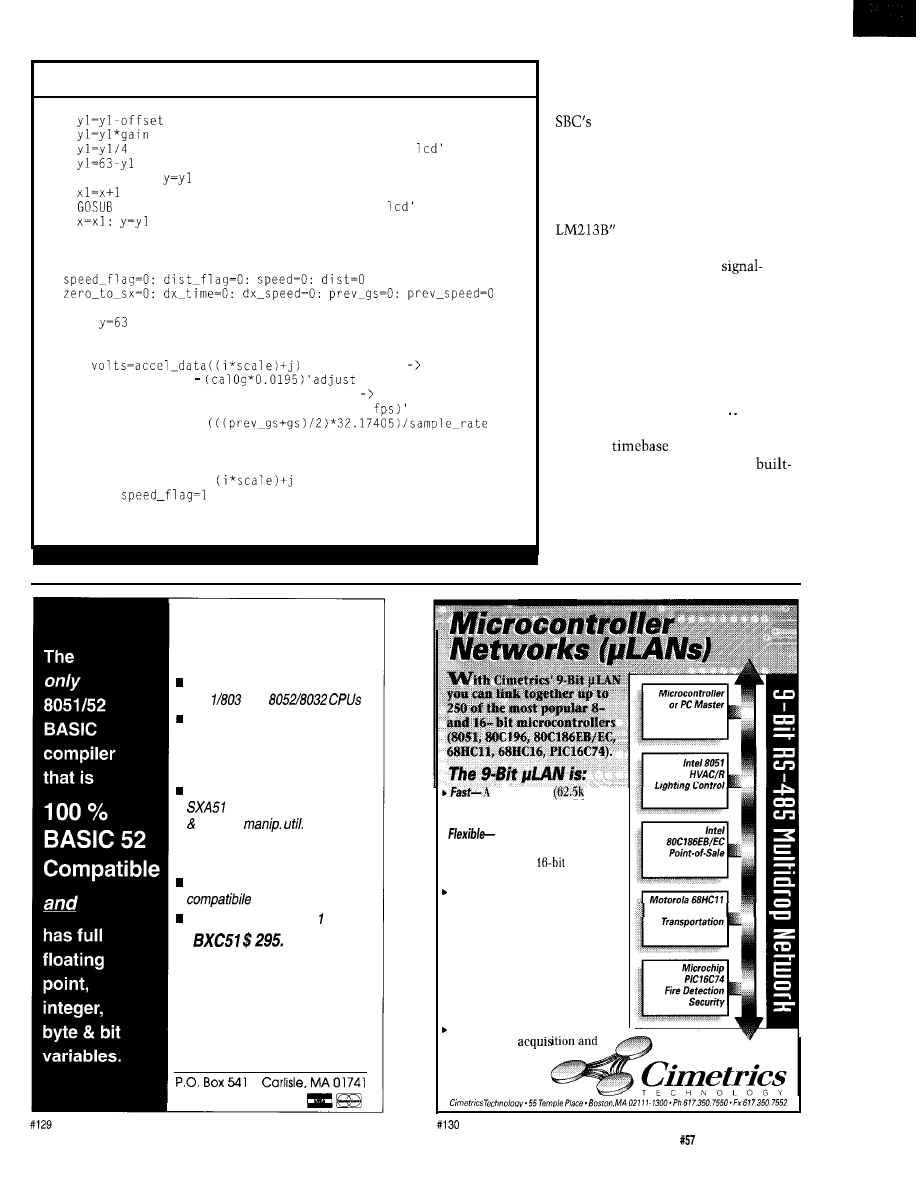
Listing
l-continued
IF i=O THEN
line
NEXT i
remove offset'
amplify signal'
and scale to fit on
flip vertical so +g at top'
start point for first line'
move to next pixel'
draw g curve on
set next line start'
'Now compute distance and plot speed'
x=8:
'start speed curve at 0 mph'
FOR i=O TO screen-size-l
'for each pixel'
FOR j=O TO scale-l
'for each sample within pixel'
* 0.0195 'a/d volts'
volts = volts
volts'
gs = volts * 2
'volts gs'
'compute velocity by integrating g curve (in
speed = speed +
prev_gs=gs
IF speed-flag = 0 THEN BEGIN
'if not sx fps yet'
IF speed >= sx THEN BEGIN
'then check for sx fps'
zero_to_sx =
'if sx fps, log time'
'and close log'
END
END
(continued)
The programs are written using
BDT (BASIC Developers Tool), which
is a high-level preprocessor for the
built-in HD64180 BASIC-180.
For a complete description of BDT,
BASIC- 180, and the logger hardware
and software (including the LCD
drawing routines), refer back to “LCD
Lineup-Getting Graphic With the
(INK 30).
Designing a data logger from
scratch calls for a detailed
processing analysis, a fancy user
interface with scrolling, zooming,
scaling, and so on, and massive storage
capability via hardware (e.g., flash
card) and software (for data compres-
sion).
Then, there’s the how you do it if
you’ve only got a few days..
Starting with the need for an
accurate
quickly leads to the
decision to rely on BASIC- 180’s
in multitasking. The tic rate is 60 Hz
and the minimal multitasking program
consists of a background program and
a single task. Why, 30 Hz sounds grand
to me-next question!
n
Memory mapped variables
n
in-line assembly language
option
Compile time switch to select
805
1 or
Compatible with any RAM
or ROM memory mapping
n
Runs up to 50 times faster than
the MCS BASIC-52 interpreter.
includes Binary Technology’s
cross-assembler
hex file
n
Extensive documentation
n
Tutorial included
Runs on IBM-PC/XT or
Compatible with all 805
variants
n
508-369-9556
FAX 508-369-9549
q
Binary Technology, Inc.
l
high speed
baud)
multidrop master/slave RS-485
network
.
compatible with your
microcontrollers
. Reliable-robust
CRC and
sequence number error checking
Efficient-low microcontroller
resource requirements (uses
your chip’s built-in serial port)
. Friend/y- Simple to use C and
assembly language software
libraries, with demonstration
programs
. Complete-includes network
software, network monitor and
RS-485 hardware
Practical-
applications
Process
Control
include data
distributed control
Circuit Cellar
INK
Issue
April 1995
101
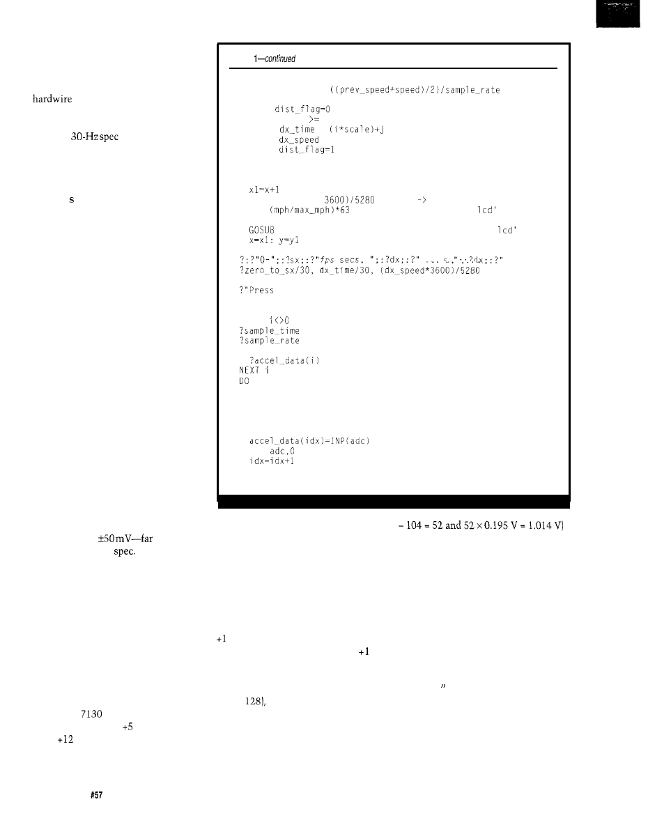
Designing a scrolling, zooming,
and scaling GUI would be neat-some
day. Instead, I simply cram everything
on a single screen and empirically
the scaling for a pleasing
display. Deciding to use 240 of the
LCD’s 256 horizontal pixels, along
with the
suggests a
minimum 8-s log time. With deadline
looming, I’m quite open to suggestion.
The maximum logging interval
required was scientifically determined
to be 80 since:
a] that’s more than enough time to end
up in the weeds and
b) 2400 elements is all that would fit
in memory.
Of course, those who are committed
(or should be) can pack the 8-bit A/D
converter readings into a character
string (rather than wasting the upper 8
bits of 16-bit integers) and use data
compression (RLL is good and
ADPCM, better) to boost storage.
The rather odd sequence of logging
intervals (16, 24, 40, and 48 s) is the
result of these decisions and the desire
for a nicely spaced horizontal axis.
Thus, all the logging intervals are
integral divisors of 240.
I must remind you that as smart
as the 7130 is, it is still analog and
subject to analog’s foibles. For in-
stance, at first I fabricated a short
adapter cable using phone wire. Firing
everything up and running a few short
tests showed a distressing amount of
noise, perhaps
worse than
the 7130 accuracy
A beginner would likely blame a
bad sensor, A/D converter, or what-
ever. Being an old-timer, I quickly
moved on to “what did I goof up this
time?” Sure enough, connecting a
known good power source quickly
proved the noise wasn’t coming from
the 7130. Dispatching with the
external wire in favor of an internal
connection cleaned everything up.
Another set of concerns surrounds
the issue of calibration. First of all, the
logger and
run on separate
supplies (the former V vs. unregu-
lated
V for the 7130). It’s not wise
to assume that each unit has the same
idea of what a volt is. Furthermore, the
Listing
'compute dist by integrating velocity curve'
dist = dist +
prev_speed=speed
IF
THEN BEGIN 'if not dx feet yet'
IF dist dx THEN BEGIN 'then check for dx feet'
=
'if dx feet then log time'
= speed
'and speed'
'and close log'
END
END
NEXT j
'set next line start'
mph = (speed *
'fps mph'
t =
'scale to fit on
yl = 63-t
'flip vert. so hi-speed at top'
line
'draw speed curve on
NEXT I
ft.
ft. mph"
a key to dump accel_data..."
DO
i=KEY
'wait for keypress'
UNTIL
FOR i=O TO sample_count-1
i=KEY
UNTIL i<>O
STOP
TASK samples
'read a/d'
OUT
'start next conversion'
'next sample pointer'
EXIT
END 'drag'
7 130 isn’t totally impervious to
temperature variations. There’s a 2%
drift in offset and span across 0-50°C.
that I didn’t bother.
So, I wrote a simple calibration
program to repeatedly sample the ADC
and average the results. Then, while
running the program, I flipped the
7130 back and forth (i.e., label up, label
down) expecting differences of 2 g (i.e.,
g to -1 g). The results read from the
A/D converter were (in decimal) g =
156 and -1 g = 104. Dividing the
difference by two yielded a virtual 2.5
V reading of 130 (versus the expected
127 or
which I plugged into the
subsequent programs.
SHOCKING DISCOVERY
Over the years, I’ve added the bits
and pieces (stabilizer bars, shocks, and
springs) to my car that make up what
Saab calls the SPG (Special Perfor-
mance Group) handling package.
At fish story time, describing the
handling differences between SPG and
stock is limited to vague hand waving
about “faster steering response,” “less
body roll, “not so floaty,” and so on.
The first tests were to document the
SPG ride.
In principle, a calibration factor
As mentioned,
SHOK. BDT
is
should be provided for the span, but
essentially the same as the first part of
my observed difference between + 1 g
DRAG. B DT so
keep referring to Listing
and -1 g was so close to ideal (i.e., 156
1. Both programs start by enquiring for
102
Issue
April 1995
Circuit Cellar INK
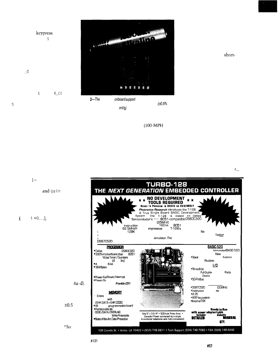
the desired log interval (i.e.,
between 8 and 80 s) and then
prompt for a
to start.
At that point, the a mp 1 es
task is dispatched with the Run
statement. If you look near the
end of the listing, you’ll see that
the s amp 1 es task takes an A/D
converter reading, stores it in the
a cc e 1 a t a array, and incre-
ments the sample count (i dx).
Meanwhile, the background task
sits in a loop, waiting for i dx to
reach the desired a m p 1
u n t .
Once sampling is done, the
amp 1 es task is canceled and
plotting of the results begin. For
each pixel (remember, we’ve got
240 of them), I compute a result by
averaging across the number of
samples that compose that pixel. For
instance, an 8-s log consists of 240
samples, so each reading is mapped
directly. Longer intervals average a
number of readings for each pixel (i.e.,
the total number of readings divided
by 240). An 80-s log has 2400 readings,
so 10 are averaged for each pixel.
Once the average is computed, a
string of y statements mutates it
into a y-axis pixel location between 0
and63. offset
are the
empirically determined constants that
make for a pleasing display (i.e., full
scale and centered). Taking care to
handle the special case of the first
pixel I F
a
line is drawn
between each pixel. Finally, the end of
the current line makes the start of the
next line in preparation for the next
pass through the loop.
For a comparison, I pirated my
wife’s ‘86 with the stock suspension.
Lest she worry needlessly, I adopted a
minor subterfuge: “I think your
fribblewumpus valve is making noise,
dear. I’ll check it for you.”
The results show that the han-
dling differences are real (Photos
Seconds are notched along the horizon-
tal access while the full vertical scale
of the display (depending on the offset
and gain constants) is about
g.
Since these are only simple
vertical g measurements, there isn’t
much to brag about. My wife summed
it up in her own pithy way,
you
spent a bunch of money to make your
Photo
7130-002s
circuits help the variable
capacitance g-sensor (silver package) deliver an accurate
typical), high sensitivity (500
output.
car ride like a truck?” Testing the true
benefits of the SPG package
sweepers, skid pad, etc.) will only
happen if headquarters agrees to cough
up bucks for a set of tires and extra life
insurance.
DAY AT THE RACES
DRAG. BDT continues on where
SHOK. BDT leaves off. Remount the
Semiconductor’s
the
*Three
l
13 Interrupts Ext. 7
second 1
Data Pointer
of Internal RAM
*Programmable Watchdog
l
amwnout Protection
Reset
*Fully supported by
accelerometer with the label
facing forward, lest you waste a
run like I did. Unlike S H 0 K, DRAG
computes actual gs, so take care
to level the accelerometer rela-
tive to the road and not the car. I
mounted the 7130 on a
angle bracket that I could bend to
account for a few degrees of rake.
Much as before, the remain-
ing portion of DRAG. B DT steps
through each pixel and each
reading within the pixel. How-
ever, this time the result is
converted to volts, adjusted with
the 2.5-V calibration factor and
turned into gs.
Knowing acceleration and
time, it’s simple to determine speed by
multiplying the two and accumulating
the result (in mathspeak, integrate
using Simpson’s rule). Knowing speed
and time, a second integration yields
distance. Along the way, the program
tracks time to speed, time to distance,
and speed at distance.
Next, the speed curve is plotted,
with scaling determined by the ma
n e w
With its 2X clock speed
and 3X cycle efficiency, an
can execute in
en
e q u i v a l e n t s p e e d
of
Equally
is the
h i g h - s p e e d N V R A M
interface. Any of the
R A M m a y b e p r o g r a m m e d d i r e c t l y f r o m a P C
t h r o u g h t h e c o n s o l e :
e l i m i n a t i n g E P R O M s a n d a s s o c i a t e d t o o l s .
P r o g r a m D e v e l o p m e n t h a s n e v e r b e e n
o r m o r e
c o n v e n i e n t , e v e n w i t h t h e f i n e s t E P R O M
T-128 features PORT 0 bias and EA-select for
upgrade.
*Modified BASIC52
l
12aK Memory Map
populated
fast NVRAM
memory
l
Gxie Space is
Now Fast Enough for
Applications
BASIC Programs and
*CALL ASM
for Maximum Speed
Parallel Ports
l
Twa
RS232 Serial
‘Decoded
I/O Strobes
Connector
UPGRADE
processor
cycle: 12 1
MIPS
82.5 MHz
ROM/l K SRAM
Comes
assembly.
utility
with
TECHNICAL
$199
in
Circuit Cellar
INK
Issue
April 1995
103
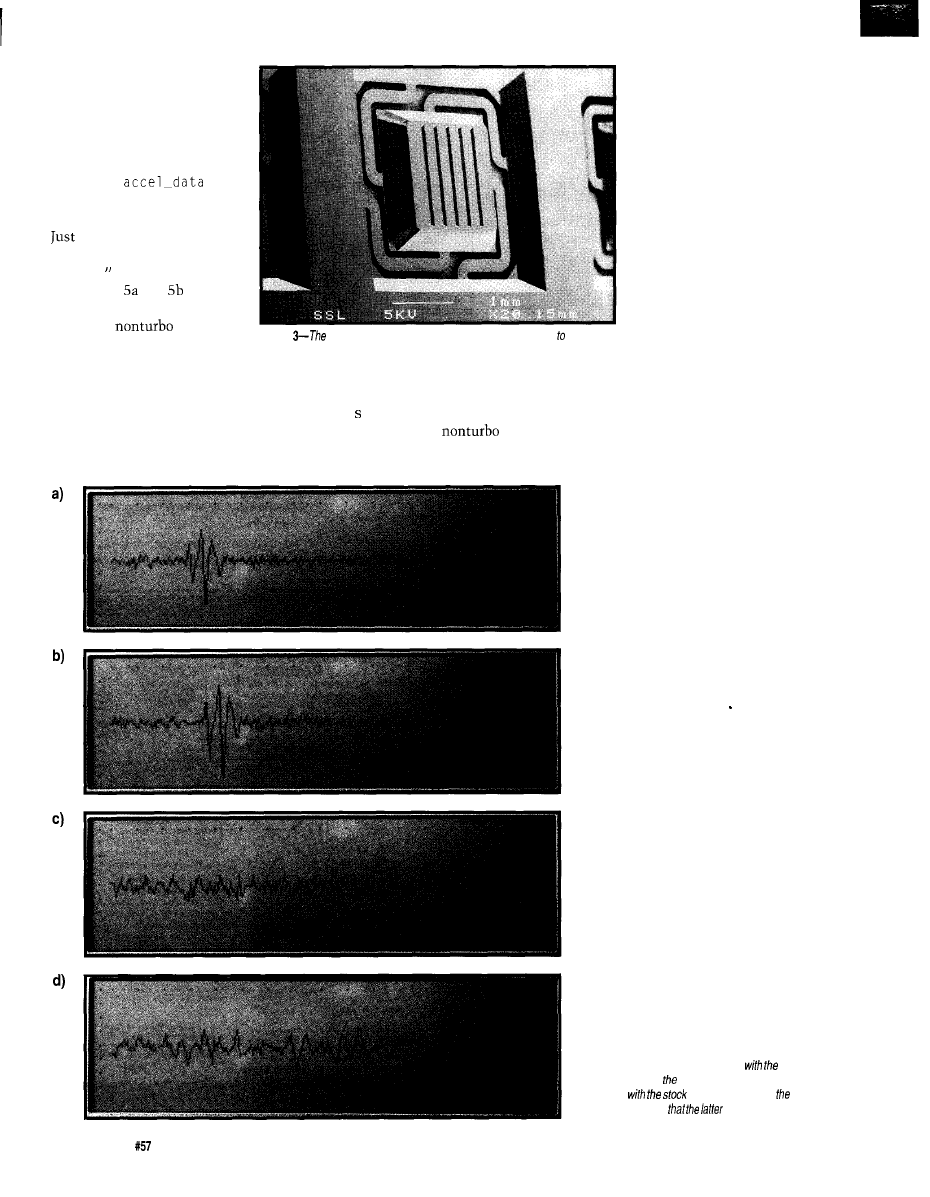
mph constant (I used 100 so
each of the 8 tics on the y-axis
represents 12.5 MPH), and the
run’s results displayed.
Finally, the program
waits for you to hit a key. It
thendumps
so
you
can capture it for plotting,
printing, or further analysis.
remember, “Any data
logged can be used against you
in court!
Photos and compare
the results of the S-speed
turbo and
auto-
matic. If you look closely, you
can see the turbo run was
Photo
7130 uses state-of-the-art micromachine techniques fabricate
the deflected mass.
marked by an exciting launch and a
the half second it took to screw up my
flattish g curve-the normal tendency
courage and it’s remarkably close to
for it to drop off is countered by the
the 10 reported in the car mags.
turbo kicking in. The program reported
By contrast, the
run is,
a 0-60-MPH time of 10.4 s. Subtract
to put it politely, sedate with only the
three-speed slushbox’s valiant
(but ultimately futile) lunge
from first to second providing
any excitement. Furthermore,
it doesn’t even live up to the
official O-60 claims, indicat-
ing some maintenance is
called for (when was the last
time I checked that
fribblewumpus valve?).
TICKET TO RIDE
Scene: Before dawn, a
deserted thoroughfare in
suburban Silicon Valley.
Officer Speed has a Saab
pulled over..
Officer Speed: You were exceeding the
speed limit and having trouble
staying in your lane.
Hapless Hacker: This may sound hard
to believe, but I’m just gathering
data on my car’s performance. See, I
write for this computer magazine
called-heck, there’s a copy in the
glove box, so I’ll just show..
Officer Speed: Keep your hands where I
can see them. How much have you
had to drink tonight?
Hapless Hacker: Oh heavens, I would
never drive under the influence. I
have enough trouble programming
as it is. I can’t even remember if
ma i n or the squiggly bracket is
supposed to come fir..
Officer Speed: What’s all that elec-
tronic equipment on the floor? You
have receipts for that stuff?
Hapless Hacker: Well, er, uh, no..
Officer Speed: Step out of the car..
Fortunately, it didn’t happen to
me, but it could happen to you. Worse,
you might get hurt. Really worse, you
might hurt someone else and that
would truly be a “sob” story.
My four-foot stepladder has a total
of eight (count ‘em!) warning labels.
Those cardboard sunscreens you stick
in your windshield have fine-print
warning “Do Not Drive With Sun-
screen In Place.” Somebody sued
because their hot coffee was hot. [I
Photo 4-Driving over speeds bumps
stock
suspension (a) and SPG (b) and driving along a
rough road
suspension (c) and
SPG
(d) c/ear/y document
is much
stiffer.
104
Issue
April 1995
Circuit Cellar INK
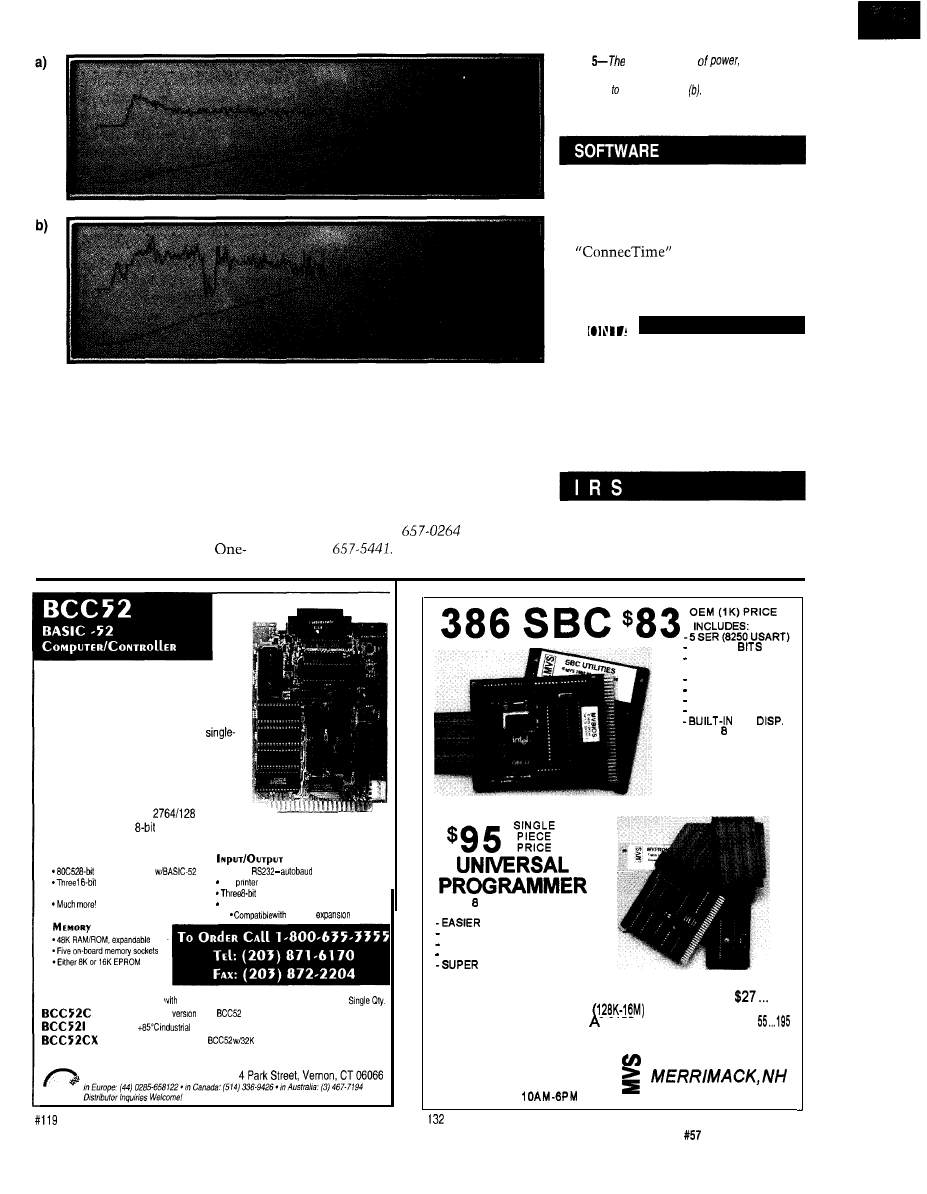
wish I could sue for all the times I got
“hot” coffee that wasn’t.)
Thus, I feel obligated to issue the
warning:
Don’t debug and drive. Always
remember to buckle up and backup.
That’s it for now, gotta run.
Tonight’s the opening of the
World Film Festival, and before that, I
want to spend a few minutes down-
stairs with my new landing gear.
q
Tom Cantrell has been an engineer in
Silicon Valley for more than ten years
working on chip, board, and systems
design and marketing. He can be
reached at (510)
or by fax at
(510)
Photo
turbo has plenty
but calls for
skilled launch technique to
exploit it
(a) while the
regular
900 seems
need a
tuneup
Software for this article is avail-
able from the Circuit Cellar BBS
and on Software On Disk for this
issue. Please see the end of
in this issue for
downloading and ordering
information.
Silicon Microstructures, Inc.
46725 Fremont Blvd.
Fremont, CA 94538
Attn: Jim Knell
(510) 490-5010
Fax: (510) 490-l 119
431
Very Useful
432 Moderately Useful
433 Not Useful
The BCC52 controller continues to be
Micromint’s best selling single-board com-
puter. Its cost-effective architecture needs
only a power supply and terminal to become
a complete development system or
board solution in an end-use system. The
BCC52 is programmable in BASIC-52, (a
fast, full floating point interpreted BASIC), or
assembly language.
The BCC52 contains five RAM/ROM
sockets, an “intelligent”
EPROM
- -
programmer, three
parallel ports, an
auto-baud rate detect serial console port, a serial printer port, and much more.
PROCESSOR
CMOS processor
counter/timers
*Six interrupts
l
Console
detect
Line
RS-232
parallel ports
EXPANDABLE!
12 BCC
boards
B C C 5 2
Controller board
BASIC-52 and SK RAM
$1
89.00
Low-power CMOS
of the
$ 1 9 9 . 0 0
-40°C lo
temperature version
$ 2 9 4 . 0 0
Low-power CMOS, expanded
RAM
$ 2 5 9 . 0 0
CALL FOR OEM PRICING
MICROMINT, INC.
3 PAR (32
MAX)
32K RAM, EXP 64M
-STANDARD PC BUS
LCD, KBD PORT
BATT. BACK. RTC
IRQO-15 (8259 X2)
0237 DMA 0253 TMR
LED
-UP TO MEG ROM
-CMOS NVRAM
USE TURBO C,
BASIC, MASM
RUNS DOS AND
WINDOWS
EVAL KIT $295
-DOES MEG EPROMS
-CMOS, EE, FLASH, NVRAM
TO USE THAN MOST
POWERFUL SCRIPT ABILITY
MICROCONT. ADAPTERS
PLCC, MINI-DIP ADAPTERS
FAST ALGORITHMS
OTHER PRODUCTS:
8088 SINGLE BOARD COMPUTER . . . . . . . OEM
“95
PC FLASH/ROM DISKS
16 BIT 16 CHAN ADC-D
. . . . . . . . . . . . . . . . . . 21 . . . . . 75
C CARD . . . . . . . . . . . . . . . . . . . . .
WATCHDOG (REBOOTS PC ON HANGUP) . . . . . 27 . . . . . 95
l
EVAL KITS INCLUDE MANUAL
BRACKET AND SOFTWARE.
MVS BOX 850
5 YR LIMITED WARRANTY
FREE SHIPPING
HRS: MON-FRI
EST
a
.
(508) 792 9507
Circuit Cellar INK
Issue
April 1995
105
John Dybowski
Using Keyboard as an
Embedded Interface
ngineers are
often charged with
the task of making
existing products do
what they were never intended to do.
This may be the natural consequence
of a product’s evolution or the result of
taking the most expeditious path to
developing something new.
When old designs become building
blocks for another technology, it’s
effective to reuse as much of an
existing design as possible. Under
certain circumstance, there may be no
other choice. This is certainly the case
when using someone else’s product as
a component of a larger system.
In using other companies’ prod-
ucts, the preferred course of action is,
not unexpectedly, the one of least
resistance. Faced with the task of
hooking a new peripheral to an
existing system, you might consider
structuring the new device’s support
code to look like the one it’s replacing.
The attraction of this common
programming trick is that it disturbs
the functioning code as little as
possible. This sort of deceptive
programming is really what device
drivers are all about.
DECEPTIVE DESIGN
Consider a thoughtfully designed
display driver as an example. With a
defined method of passing input and
output arguments and generic func-
tions for standard operations such as
device initialization, the main program
could care less if the actual output
device was an LCD, vacuum fluores-
cent panel, CRT terminal, or anything
else with a similar set of features.
At the other extreme, the conse-
quences of embedding device depen-
dencies directly into your process code
can prove to be intolerably restrictive
should a change be ultimately re-
quired. The fact is, even if you are
content to specify a specific peripheral
for a given application, who’s to say
the manufacturer will be able to
deliver a year from now. Stuff happens.
This is not to say that incorporat-
ing device-specific functions in your
code is necessarily bad. Certainly,
there are cases where efficiency
dictates that we stray from the
a system processor doesn’t have the
required throughput for a heavily
layered device-support structure.
However, be aware of the tradeoffs.
Simply put, it’s okay to write bad code
if there’s no other way to do it.
This may seem to be quite a
foolish statement. But realize that
there are definitely a number of very
popular processors that make writing
good code very difficult, if not impos-
sible. This is especially true of some of
the very low-end controllers that
present a varied and unending assort-
ment of ways to cramp your style-a
meager and irregular instruction set,
bizarre program-memory paging
schemes, or diabolically restricted
addressing modes. Sound familiar?
Device drivers essentially offer a
stylized means of defining
passing conventions between program
modules. The inherent benefits,
however, shouldn’t be limited to
modules with a formally defined
interface specification.
It’s often equally advantageous to
use this programming technique
within the depths of your program for
changing the way calls and
functions operate. When faced with
the prospect of replacing major
function blocks, I go out of my way to
make the new code imitate the
original’s I/O conventions. The goal:
don’t let the main program know
there’s a difference.

This type of imitation, applied to
hardware devices, is commonly
referred to as
emulation.
EMULATE THIS
A standard device that can be
emulated advantageously is the IBM
keyboard. By knowing how the IBM
keyboard electronics and communica-
tion protocol are structured, a wide
variety of equipment can be compelled
to function as either a sending or a
receiving device.
The wide availability of very small
IBM-compatible computers designed
for embedded applications extends the
potential for this standard interface. It
would be an advantage to use the BIOS
keyboard-support services regardless of
the form your keypad took. Alterna-
tively, although unquestionably of less
utility, you might connect your
proprietary embedded controller to a
standard PC keyboard.
Another possible use for keyboard
emulation may not have anything to
do with a keyboard at all. Consider an
application where you have to enter
data collected by an embedded instru-
ment into a spreadsheet or some other
program running on your desktop PC.
Since most data collection devices
have some sort of serial interface, you
might be tempted to first obtain a
printout and enter it into your com-
puter manually. Although requiring
the least
work, this approach
has the disadvantage of being time
consuming and error prone.
A step toward automating the
procedure may involve capturing the
serial data to a file for later processing.
Or, you might feel creative and write a
little TSR that intercepts data from the
serial port and deposits it into the PC’s
keyboard buffer. This back-door
approach could save you the interme-
diate steps otherwise required in
preparing your filed data for input into
your PC program.
A more direct approach simply
makes the data look like it’s coming
from a keyboard in the first place,
bringing it through the keyboard port.
Obviously, this method can only
be applied to a limited number of
collection tasks. If it is suitable for the
volume and the nature of the data
you’re manipulating, there are several
distinct advantages. Not to be underes-
timated is the fact that all your
alterations are made far away from the
stuff that’s already running!
STANDARDKEYBOARDS
The IBM-compatible keyboard has
gone through two transformations: the
PC/XT and the AT keyboards. As
you’d expect, both designs use built-in
microcontrollers to manage the matrix
scanning and handle communications
to the computer. The original PC/XT
computer used nothing more than a
shift register and flip-flops to receive
data transmitted by the keyboard.
Starting with the AT, the com-
puter interface consists of a slave
microcontroller that acts as an
Figure l--The circuitry inside the
keyboard (shown here) is very similar to that in an AT keyboard. The main
differences are in the firmware.
intermediary for all bidirectional
communications to and from the
keyboard. The added capability of the
AT’s keyboard-communication
processor opens up the potential for
managing a lot more complexity in the
keyboard-communication protocol.
Although the PC/XT-style
keyboard has deficiencies, it also has
(of necessity) the virtue of simplicity.
With this in mind, let’s see what the
two types have in common before
examining the older design and how it
was transformed into the ubiquitous
AT configuration.
The concept common to both
PC/XT and AT keyboards is that
physical key scanning is carried out
under control of an
microcon-
troller. The controller detects when a
key is pressed and released and sends
this information to the computer.
Rather than outputting standard
ASCII codes, IBM keyboards attain
greater flexibility by transmitting
make and break scan codes as keys are
pressed and released. These scan codes
are assigned by numbering the physi-
cal keys on the original PC/XT
keyboard from left to right, top to
bottom. It’s up to the computer’s BIOS
to convert these unique codes into
ASCII codes when possible. Special
keys that don’t have corresponding
ASCII symbols are given a null value
followed by the scan code. This null
causes the computer to properly
interpret the following code as a scan
code rather than an ASCII code.
Communication between
the keyboard and computer is
accomplished over a data line
and a clock line. These lines
are driven by open-collector
devices with their associated
pull-up resistors at either end.
A typical keyboard line
interface is depicted sche-
matically in Figure
1.
THE PC/XT KEYBOARD
Figure 2 shows the
original PC/XT computer’s
keyboard interface. As you
can see, this hardware
implementation centers
around a shift register and
several flip-flops. Data bits
Circuit Cellar INK
Issue
April 1995
1 0 7
Figure
original IBM PC’s keyboard
consisted of just a
register and some glue logic and could only receive data from the keyboard.
are shifted in on falling edges of the
keyboard-generated clock and are valid
from before this falling clock edge
until after the rising edge of the clock.
The data line registers a high start
bit and eight data bits for each trans-
mitted code. Looking again to Figure 2,
you see that initially a reset signal
clears the shift register and its associ-
ated flip-flop. As data bits are clocked
in, the high start bit propagates
through the shift register and appears
at the ninth-bit flip-flop. This asserts
an interrupt on the CPU.
At the same time this flip-flop
pulls the clock line low. This signals a
busy state to the keyboard, which is
held until the received character has
been processed by the computer. Once
this busy status clears, the clock line
is released and is pulled high by the
pull-up resistor. This indicates to the
keyboard that the interface is available
for further transmissions.
Curiously, with the interface in its
idle state, the keyboard lets the clock
108
Issue
April 1995
Circuit Cellar INK
line pull high, but drives the data line
low. This turns out to be an unfortu-
nate decision on the part of the design
engineers for it essentially jams the
data line, making bidirectional
communication impossible.
As a result, it’s not possible to
have multiple transmitting devices on
the line without adding extra circuitry
to minimally disconnect the
keyboard’s data line from the rest of
the interface. Because of the way make
and break codes are represented, the
PC/XT keyboard is capable of encoding
128 different key codes. A byte with a
value of O-127 is a make code. Adding
80 hex to this basic code creates a
break code. For example, if Olh is the
make code, 81h is the break code.
THE AT KEYBOARD
The AT keyboard rectifies some
shortcomings of the PC/XT keyboard
while introducing a level of complex-
ity that seems a bit out of place in a
keyboard. Remember that the AT
computer’s keyboard port uses a
dedicated microcontroller to manage
all communications with the key-
board. This explains why things get
complicated. Simply put, with the aid
of this additional processing power,
getting complicated is easy to do.
The AT interface is defined as
bidirectional. The data line is now left
pulled up while no data is being
transmitted or received so either the
keyboard or the computer can take
control of the interface during idle
times. As I’ll show later, this also
leaves the possibility of adding other
external devices that can easily seize
control of the interface.
Bidirectional data communication
between the keyboard and computer
consists of 1 l-bit datastreams com-
posed of a low start bit, eight data bits,
an odd parity bit, and a high stop bit.
The clock and data relationship
remains similar to that of the PC/XT.
A fairly comprehensive [for a key-
board) protocol is defined that provides
for error detection and retransmission,
abort timing, and a line-contention
recovery. Additionally, a relatively
complete command set is specified
that describes a number of useful (and
not so useful) functions that the
keyboard and computer can initiate.
As with the PC/XT keyboard, all
keys are handled on a make/break
basis. The difference is that to handle
more than 128 keys, a different
method of denoting break codes is
used. Break codes are transmitted as
followed by the hex make code.
Now a make and break sequence for
scan code 1 appears as
The AT’s keyboard-interface
electronics are very similar to those
used in the PC/XT. The computer’s
interface is implemented in firmware
running on a microcontroller, so it’s
pointless to try to depict it schemati-
cally. It’s just your typical black box.
NEGOTIATING THE WIRE
With both the PC/XT- and
style keyboards, all communications
are carried out using open-collector
drivers on the clock and data lines.
With the PC/XT, there’s not much
more to a typical transaction than
what I’ve already said. This is partially
due to the fact that the interface is
capable of unidirectional traffic only
and in part because you can only get
into so much trouble with a shift
register and some glue.
The situation is a little more
interesting with the AT.
elaborate
more fully on how the keyboard and
computer negotiate for control of the
line and what happens if there’s a
conflict. As stated, when no
cation is occurring, the data and clock
lines are held at a high level through
pull-up resistors. The use of
collector drivers allows either end to
assert a logic low on either of the
interface lines.
the computer is doing some-
thing, it may elect to hold off a
keyboard transmission by pulling the
clock line to a low level (inhibit
status). In a similar fashion, the
computer signals its intention to begin
transmitting by asserting a low level
on the data line while leaving the
clock line at a high level (RTS status).
If either condition is in effect, the
keyboard will not attempt to transmit.
Note that when the computer asserts
request-to-send (data line low), it puts
its start bit on the line. On recognition
of this event, the keyboard proceeds by
emitting 11 clocks. The first 10 strobe
in the start bit, eight data bits, and the
parity bit. After the tenth bit, the
keyboard pulls the data line low and
issues one final clock pulse. This
keyboard-generated stop bit signals the
computer that the keyboard has
received the transmission. The
computer returns to a ready state or
puts the interface into inhibit status.
The keyboard checks for inhibit
status and request-to-send status prior
to starting any data transmission.
Once a transmission has been initi-
ated, the keyboard must continuously
check the clock. Should the computer
lower the clock line while the key-
board is transmitting, the interface
enters a state called line contention.
What happens now depends on
how far into the sequence the key-
board is. If this contending state is
recognized before the rising edge of the
tenth clock (the parity bit), the
keyboard releases the clock and data
lines and retains the pending data for
later retransmission. If line contention
occurs after the tenth bit, the trans-
mission is assumed to have “gone
through” and the transfer concludes
normally. On receipt of the keyboard’s
data, the computer puts the interface
into inhibit status if it needs extra
processing time or a response request
is to be issued.
US VERSUS THEM
When IBM developed the AT
computer, it’s obvious they had the
resources to put together a design team
just to handle the keyboard design. For
those of us with lesser means, it’s
important to separate the essential
from the superfluous. That is, we have
to cut through the fluff. Through
empirical observation, some generali-
zations about the operation of the AT
keyboard can be made.
For example, for most keys, only
their respective make codes are
significant. The complementary break
codes are unessential and make no
Add these numbers
up:
a ‘51 Compatible Micro
40 Bits of Digital I/O
8 Channels of 10 Bit A/D
3 Serial Ports
or
2 Pulse Width Modulation Outputs
6 Capture/Compare Inputs
1 Real Time Clock
64K bytes Static RAM
+
UVPROM Socket
512 bytes of Serial EEPROM
1 Watchdog
1 Power Fail Interrupt
1 On-Board Power Regulation
It adds up to real
power!
our popular
priced
just $299 in single quantities.
Yot enough I/O? There is an
bus, too! Too much
We’ll create a version just for
needs, and pass the savings
to you! Development is easy,
our Development Kit: The
Development board
ROM Monitor, and an 8051 C
compiler for just $449.
popular 803
can now be
shipped with your favorite 8051
family processor. Models include
FA,
BOC652,
and
Call for pricing today!
The
Plus is a low-cost
to conventional ICE
Load, single step,
nterrogate,
disasm, execute to
Only $448 with a pod.
the 8051 family, including
and Siemens derivatives.
for brochure!
Equipment Corp.
9400
Road
San Diego, CA 92126
(Fax: (6 19) 530-l
S i n c e 1 9 8 3
(619) 566-l 892
Internet e-mail: info@hte.com
Internet ftp:
Circuit Cellar INK
Issue
April 1995
109
difference to the computer. It appears
the PC BIOS only uses the break codes
for keys such as Alt, Shift, and Ctrl.
This may not be particularly signifi-
cant if all you’re doing is developing a
compatible keyboard. If, on the other
hand, you are translating ASCII data to
emulate a data stream that merely has
to look like it’s coming from a key-
board then this knowledge can save a
lot of unnecessary line traffic, not to
mention wasted code.
And speaking of traffic, a lot of the
protocol’s intricacy exists to handle
data errors, count abort times, and sort
out line contentions. Somewhat
associated to this is the command set
that defines a multitude of functions
the keyboard and computer are to
support. Adherence to the rigors of the
specification depends on what you’re
trying to accomplish. Experience
shows that just clocking your data
across the interface yields satisfactory
results for a wide range of applications.
Regardless of the degree to which
you’re intending to emulate a real
keyboard, there are several issues you
should carefully consider. For instance,
there are a number of pitfalls if your
emulation device must operate in
conjunction with a “live” keyboard.
Keeping track of the state of the
keyboard/computer interface is not
something you want to take lightly.
Recall that certain key codes are
capable of causing the system BIOS to
effectively redefine the attributes of
the majority of the keys.
For example, consider that your
emulation device inadvertently seizes
the interface after a Ctrl make code is
sent by the keyboard. Obviously, the
data ultimately seen by the PC
application differs substantially from
what you intended.
It would perhaps be even more
disturbing to corrupt the Ctrl break
because of a data collision. Here,
hopefully the communication protocol
would bail you out.
You might consider providing
special lockout circuitry on your
interface that disconnects the key-
board from the computer when your
device is sending data. Here again, you
could potentially get in trouble if
certain make/break sequences were
110
Issue
April 1995
Circuit Cellar INK
Listing
AT keyboard driver performs fine for programs that use
keyboard
ENTRY POINT
PUBLIC
REFERENCES
EXTRN
BIT
EXTRN
BIT
EXTRN
BIT
SHIFT
CONTROL EOU
BREAK
INTO CODE SEGMENT
SEGMENT CODE
RSEG
PROG
TO SEND DATA STRING TO AT VIA KEY PORT
RO=BYTE COUNT
FOR
SOURCE (IF
DPTR=POINTER FOR XRAM SOURCE (IF
MOV
JNZ
ATXO
RET
TRANSMIT LOOP
ATXO:
JB
MOV
INC
SJMP
MOVX
INC
MOV
CALL
JZ
CJNE
SJMP
SEND_EXT,ATXI
DPTR
XCHAR
ATX5
ATX4
SHIFTED CHARACTER
ATX3:
CALL
XMIT
DJNZ
RO,ATXO
RET
CHARACTER
ATX4:
MOV
CALL
MOV
CALL
CALL
MOV
CALL
MOV
CALL
XMIT
XSHFT
XMIT
XMIT
XMIT
TO SEND?
SOURCE?
ASCII
;GET ASCII
ASCII
ON
ASCII
CODE
OFF
(continued)
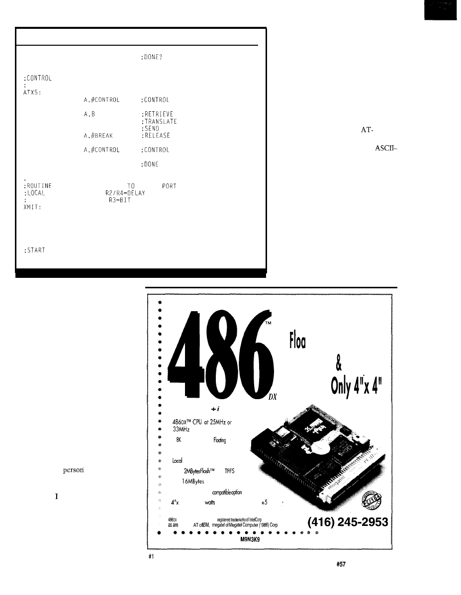
Listing l-continued
DJNZ
RO,ATXO
RET
CHARCTER
MOV
ON
CALL
XMIT
MOV
ASCII
CALL
XSHFT
CALL
XMIT
CODE
MOV
CALL
XMIT
MOV
OFF
CALL
XMIT
DJNZ
RO,ATXO
RET
To
S
END A CH
A
R A
C
TER
AT KEY
REGISTER USAGE:
LOOP COUNTER
COUNTER
;INTERCHARACTER DELAY FIRST
CALL
DELAY
BIT
(continued)
disassociated. In such a situation, an
undetected, lost keyboard transmis-
sion would be even more likely.
With a little extra hardware you
could hold off the keyboard while you
are transmitting by asserting an inhibit
status on the [now isolated) keyboard
interface. In such a scenario, constant
line monitoring of all transmissions
from the keyboard and computer
would be necessary.
What all this boils down to is that
you require a little smarts of the
person operating the equipment or you
can put a lot of smarts in your equip-
ment. Sometimes, the former consti-
tutes an unreasonable assumption.
Then again, you have to give realistic
consideration to the system’s operat-
ing conditions. The fact might be that
in some cases a
would really
have to work to break it.
Putting things into perspective,
the situation described is not nearly
as much of a problem in a typical
system implementation as would seem
at first. However, looking at things on
a detailed level flags the hazards of a
particular approach. Walking the line
between too much and too little is
always difficult and often involves
subjective judgment calls. Sure, you
can render a design to handle all
eventualities, but you might price your
product right out of the market.
KEY CODE AND
UNEXPECTED APPLICATIONS
In keeping with my usual premise
of starting simple, I’ll present a
rudimentary transmit-only
keyboard emulation driver. For
flexibility, the code includes an
to-scan-code translator.
As an interesting side note, this
code is similar to something I devel-
oped several years ago as part of a
remote computer-control center. It
turns out that some of the most
intriguing applications may be totally
unexpected and unforeseen, which is
exactly what happened. Through a
fortunate sequence of events, one of
my systems eventually found its way
into the hands of some rather inven-
tive software developers. It was just
the thing they were looking for.
W O R L D ’ S S M A L L E S T
The PC/II includes:
.
clock frequency
. Full
Cache with
Point
. Ethernet local Area Network
l
Bus Super VGA Video/LCD
. Up to
with
. 4 or
User DRAM
.
PC/l
04 or ISA Bus
(wih adapter)
.
4” Format; 6
power consumption at volt only
Embedded PC with
ting Point,
Ethernet Super
VGA
and Flash are
PC,
l
125 Wendell
Ave.
l
Weston, Ont.
l
l
Fax:
(416) 245-6505
megatel”
Circuit Cellar INK
Issue
April 1995
111
FREE
Data Acquisition
Catalog
acquisition catalog
from the inventors of
plug-in data acquisition.
Featuring new low-cost
A/D boards optimized
for Windows,
DSP Data Acquisition,
and the latest
Windows software.
Plus, informative
technical tips and
application notes.
Call for your free copy
l-800-648-6589
ADAC
American Data Acquisition Corporation
70 Tower Office Park, Woburn, MA 01801
p h o n e 6 1 7 - 9 3 5 - 3 2 0 0 f a x 6 1 7 - 9 3 8 - 6 5 5 3
112
Issue
April 1995
Circuit Cellar INK
Listing l-continued
CLR
KEY-DATA
NOP
CLR
MOV
DJNZ
SETB
FOR LOOP
MOV
MOV
C
BIT BANGING LOOP
RRC
MOV
NOP
CLR
MOV
DJNZ
SETB
DJNZ
STOP BIT
SETB
NOP
CLR
MOV
DJNZ
SETB
RET
A
KEY_DATA,C
KEY-DATA
LOW
LOW
HIGH
COUNTER
PARITY
DATA
LOW
HIGH
HIGH
LOW
HIGH
INTER-CHARACTER DELAY RO
U
TI
NE
MOV
MOV
DJNZ
DJNZ
RET
TRANSLATE ROUTINE
INC
A
MOVC
RET
LOOKUP TABLE
;O=CONTROL CHARACTER,
DB
DB
DB
DB
DB
DB
DB
DB
DB
DB
DB
DB
(continued)
These people had written a rather
complex PC application and were
adamant about testing it thoroughly
before permitting even a beta release.
Manually testing from the keyboard
was not deemed feasible due to the
number of input permutations and the
likelihood of operator error.
At the same time, they were
skeptical about the possibly disruptive
effect of performing the final testing
using the special TSR they had used
during the initial check out. In short
order, they had written a special
program designed to run on a dedicated
computer that operated the remote
computer-control system as a robot
typist. The test sequence ran at
maximum speed for 24 hours a day
over a period of three weeks! Due in
great part to this test plan, when the
software shipped, it was remarkably
bug free.
Anyway, back to the code. Listing
1
is the AT-keyboard emulation driver
presented in its entirety. The program
includes both an ASCII-to-scan-code
translation algorithm and a bit-banged
scan-code transmission routine. This
803
1
assembly-language code can
accept its input string in either
internal or external RAM. The charac-
ter count is passed in register RO, the
internal RAM data pointer uses
and the external RAM data pointer
uses DPTR. The bit variable S END_
E XT determines whether the input
string resides in internal or external
RAM.
On entry, RO is checked. If it does
not contain 0, (an errant null string),
the code falls through to the main
data-transmission loop. Now a data
byte is picked out of the appropriate
data area in accordance with the
bit flag.
The initial ASCII translation is
performed by XC HA R, which returns
either the actual scan code or a special
indicator. If the returned value is
neither
nor
then no further
processing is required. The scan code
is dispatched to XM I T and is clocked
out to the computer. A returned value
of
indicates the ASCII character
requires a shift operation whereas a
means the ASCII character
involves a control operation.
114
Issue
April 1995
Circuit Cellar INK
Listing
DB
DB
DB
DB
CHARCTER TRANSLATE ROUTINE
INC
A
MOVC
RET
T A B L E
DB
DB
DB
DB
DB
DB
DB
DB
DB
DB
DB
DB
DB
DB
END
The shift code is handled by first
outputting a shift make code. A
secondary lookup using X S H FT trans-
lates the original ASCII code to a scan
code. This code is transmitted, fol-
lowed by a break code and a shift code
(shift break sequence). The procedure
for a control code is similar, except the
sequence is framed with a control scan
code. These basic steps repeat until the
character count in RO is exhausted.
The code works okay, but is not
without its problems. No attempt is
made to determine the actual opera-
tional status of the
computer interface. The rather flagrant
assumption is made that the interface
is in normal mode-that is, not in a
state such as Shift, Ctrl, Alt, Caps
Lock, and so on.
Also, note that strings involving a
lot of shifted sequences suffer a
significant performance penalty since
each ASCII character results in the
transmission of three codes in addition
to the translated scan code: a shift,
break, and shift. Obviously, if I were to
improve this program, keeping track of
my own shift status would be one of
the first areas I’d address.
Next month, I’ll wrap up with a
discussion of the AT-keyboard com-
mand set, scan-code tables, and a few
other details I was forced to omit this
month because of space constraints.
I’ll conclude with a demonstration of a
real application based on the material
presented.
Dybowski is an engineer in-
volved in the design and manufacture
of embedded controllers and commu-
nications equipment with a special
focus on portable and battery-oper-
ated instruments. He is also owner of
Mid-Tech Computing Devices.
may be reached at (203) 684-2442 or
at
434
Very Useful
435 Moderately Useful
436 Not Useful
The Circuit Cellar BBS
bps
24 hours/7 days a week
(203)
incoming lines
Internet E-mail:
It’s
been a busy month of upgrades on the BBS. We received a new
version of the BBS software that completely replaces the file section
interface with one that allows full-screen selection of
for batch
downloads. There are lots of other small improvements as well.
Our Internet provider also upgraded their pipeline from a 56k
line a We should see an improvement in mail and newsgroup
delivery times as a result.
In this month’s threads,
with a discussion of the proper
way measure an RS-422 line. Since it’s a differential signal, it’s not
as easy as touching a
single scope probe the line.
Next, we look at decoding a low-speed datastream coming
through a
radio system. There is more to this thread than
would fit within these pages, so if it sparks your interest, give the
BBS a call and read the whole thing.
Finally, if’s time to cut some foam with a heated wire, but how
do you design the drive electronics for such a wire?
Measuring RS-422 signals
From: Dan Walker To: All Users
What is the proper way to measure RS-422 if you want
to check the amplitude and the condition of the waveform?
I have been measuring from the positive terminal to ground
with a Fluke Scopemeter. I have heard some people say you
should measure from the positive terminal to the negative
terminal with the scope.
From: James Meyer To: Dan Walker
I’d measure first one side with respect to ground and
then the other. In most cases, they will be mirror images of
each other. If they aren’t, then something’s not quite right
somewhere.
If you take only *one* measurement, either side to
ground or differentially between sides, you could miss
something important.
From: John
To: Dan Walker
Gosh, you’ve got an isolated scope-just measure from
positive to negative. It is a differential standard and looks at
the difference between positive and negative. The idea is to
by Ken Davidson
reject all the common-mode crud that is present on both
wires. Your Fluke Scopemeter is the ideal instrument to
make these types of measurements. If you measure one
wire or one wire at a time, you really can’t tell anything
unless there is no common-mode noise and there is a path
to ground somewhere. Theoretically, the signals have no
relation to ground, in practice there is a
mode limit.
From: Pellervo Kaskinen To: Dan Walker
As is so often, it depends..
If you have limited facilities, you measure what you
can. If that does not appear to adequately cover your
information needs about the waveforms, you take the next
more complicated approach.
I personally prefer always making two measurements
on the differential signals, maybe three. The two measure-
ments can be any combination of the actual difference
signal and one polarity versus common or the two signals
against common at the same time. In the last case, I can
mentally process the difference.
But most of the time it is just so simple to turn the two
channels of the scope into a quasidifferential mode. If I have
the two signal lines attached and a difference displayed,
then I can turn one input selector to grounded position and
I see the individual signal of the other line. I can flip this
over as many times as I want with minimal effort.
The reason I want to see the individual signal(s) is that
there can be a common-mode level in excess of the receiver
or transmitter capability. The differential display may or
may not reveal that possibility. On the other hand, it is the
differential signal that is supposed to carry the information.
If I do not measure that, I’m assuming too much.
Low-speed data
From: Ben Stedman To: All Users
I’m looking for suggestions on how to decode some
low-speed data that’s used in a
radio system. The
data is used to steer mobile radios to the proper repeater and
Circuit Cellar
INK
April1995
115
to identify them to the system to provide a small measure
of privacy. The particulars are:
Bit rate: 300 bps
Message length: 40 bits
Repetition rate: continuous
As far as I know, there is no framing on the individual
parts of the message, however there is a sync pattern
consisting of 101011000 (9 bits) at the start of each message.
The entire message looks like this:
9 bits sync
1 bit area
bits
repeater
bits home repeater
8 bits id code
bits free repeater
7 bits checksum
Should I monitor the incoming bits until a match is
found with the sync pattern and then save the next 31 bits?
Or should I read 40 bits into a buffer and then scan the
buffer for the sync pattern? Or is there some other good
method?
I plan on using a PIC or an 803 1 to do the processing
and then display the information an a LCD. Thanks in
advance for any ideas and comments.
From: Russ Reiss To: Ben Stedman
As they say, Ben, there are many ways to skin a cat.
Any method that gets the job done is usually OK, but it
would seem to me that it is simpler to just keep monitoring
the input until you see the sync code, then grab the follow-
ing 3 1 bits and use them. Otherwise, you need to feed
everything into a circular buffer, mark the location of the
sync (when you find it), and keep everything else in sync
with that position. It certainly can be done, but sounds
more complex than the first approach, and I can’t see what’s
gained by it. Just be sure that the sync pattern is truly
unique and cannot appear as some combination of data in
other fields (presumably the designer of the encoding
technique thought of this!)
Sounds like an ideal project for a PIC chip. You might
check out my June ‘94 article in INK for how simple
development would be with a
Their EEPROM
capability makes them ideal for “interactive” development
of a project like this. Seldom does the code work right the
first time, and once you get it running, you always think of
new things to add. You typically end up unplugging, UV
erasing, and reinstalling many, many chips in this process.
116
Issue
April 1995
Circuit Cellar INK
That’s why I so much enjoy
reprogrammable
micros like the ‘84.
From: James Meyer To: Ben Stedman
would start out by putting the pulse string into my
desktop PC first. A little bit of fiddling around with various
methods of detection there would be *much* easier than
the compile..
method of starting out directly on the microcontroller.
Either that, or I would use a simulator program for the
target micro that I could run on the PC.
Meyer’s Maxim
“A peek at the answer is worth a
thousand guesses.”
At least it worked for me during high school..
From: Dave Tweed To: Ben Stedman
What you have is called a “framed” data stream, and
the Y-bit pattern is called the “frame pattern.” Finding and
maintaining frame alignment in a potentially noisy (i.e., full
of bit errors) channel is nontrivial, but not terribly difficult,
either.
First of all, you cannot assume that the frame pattern
will not appear elsewhere in the data stream. The only way
to confirm that you have the correct frame alignment is to
check that it repeats at the expected
frame period.
False frame patterns will not.
The general technique is to have two states in the
software: in-frame and out-of-frame. When you are
frame, you search the incoming data bit-by-bit until you
find a valid frame pattern, then go in-frame. When you are
in-frame, you split out the individual data fields, and then
check for another frame pattern.
Here’s where things get tricky-if you don’t find
another frame pattern, you do not necessarily want to go
out-of-frame immediately. You may want to see if only one
or two bits are wrong and stay in-frame if so. You may
simply want to wait for another frame period and only go
out of frame if you fail to see the frame pattern two or three
times in a row.
Note that you do not necessarily need to buffer the
incoming data; you can do all of this on the fly as the bits
come in.
By the way, 300 bps sounds easy-the systems I build
normally do this sort of thing at I.544 Mbps and up. I also
have some experience with trunking radio systems.
Also, the
“checksum” on a 40-bit message sounds
more like an error-correcting code-you can use it both to
verify frame alignment and to greatly improve the overall
reliability of the data. In a *really* noisy environment, you
could even go so far as to apply the error-correction
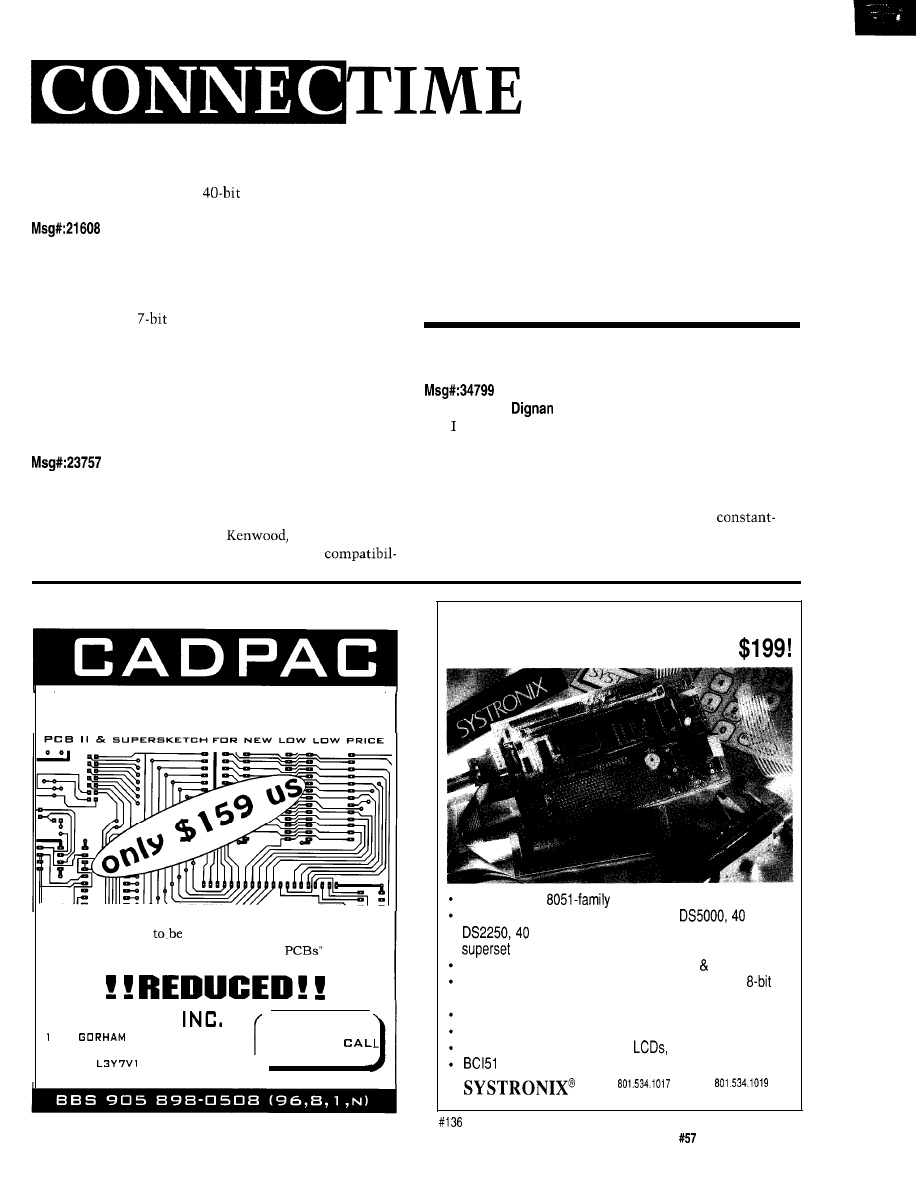
rithm at every possible frame alignment when out-of-frame.
In this case, you’d need the
buffer.
From: Ben Stedman To: Dave Tweed
Thanks for the info concerning framed data streams. I
think it will be relatively straightforward to code the
technique you suggest.
As far as the
error-correcting code at the end of
each packet goes, I have no definitive information as to how
it is calculated, but since this is an “educational experi-
ence” project, I can just ignore it for now.
However, the next step is to attempt to *encode* this
information as well, and I guess I’ll need to study those last
7 bits carefully.
From: Michael Millard To: Ben Stedman
From your description and my knowledge of trunking
formats, it looks like you are describing an EF Johnson LTR
format. This comes in Uniden,
Trident, Zetron,
and other flavors, but for the sake of backward
ity, none change the actual repeater data bus. At least not at
the tower site location. Mobile formats may differ slightly
depending upon signaling options.
LTR is an open-system architecture. You can save
yourself a lot of headache by just asking for the specifica-
tion from the respective manufacturers or see the EF
Johnson Trunking System Specification Literature.
Wire heating
From: Andrew
To: All Users
am trying to find a way to keep a wire at a constant
temperature. The wire is cutting through a foam insulating
material, the ends being a foam core wing for aircraft. At
present I am using an AC variable transformer to control
the temperature but am looking for something a little more
controlled and automatic.
I
would guess that a
current power supply would be the answer? Are there
circuits out there that can handle this? The power demands
P C S
A N D
S C H E M A T I C T O O L S
2 for the price of 1
** features comparable
to
packages costing
thousands!
** must be tried
believed
**“easiest product to use for designing
** customers call it “the 8th wonder of the world!”
R4 SYSTEMS
1 DO
ST. S
UITE
1 1 B-332
NEWMARKET ONTARIO
CANADA
9 0 5 8 9 8 - 0 6 6 5
F A X
F R E E D E M O
W R I T E O R
T O D A Y
9 0 5 8 9 8 - 0 6 8 3
NEW! UNIVERSAL DALLAS
DEVELOPMENT SYSTEM
from
It’s a complete
single board computer!
One board accommodates any 40 DIP
SIMM
SIMM DS2252, or 72 SIMM DS2251, 8051
processor! Snap one out, snap another in.
Programs via PC serial port. Program lock encrypt.
LCD interface, keypad decoder, RS232 serial port,
ADC, four relay driver outputs, four buffered inputs.
Power with 5VDC regulated or 6-13 VDC unregulated
Large prototyping area, processor pins routed to headers
Optional enclosures, keypads,
everything you need
Pro BASIC Compiler w/50+ Dallas keywords $399
T E L :
F A X :
555 South 300 East, Salt Lake City, UT, USA 84111
Circuit Cellar
INK
Issue
April 1995
117

are from 50 to 100 watts. Any suggestions? Thanks ahead of
time.
From: James
To: Andrew
have made my own foam cutter using a variable
transformer and a transformer salvaged from a microwave
oven. The variable transformer feeds the primary side of the
microwave transformer. The microwave transformer has
had the secondary winding removed and replaced with 12
wraps of
insulated wire. This whole mess heats a
length of 0.032” wire made of 304 stainless steel
safety wire). This circuit is not automatic, but it works very
well and keeps the
factor in the safe range. Experi-
ment with the number of wraps around the microwave
transformer so you have the desired temperature of the wire
at midrange on the variable transformer.
I think a constant-current power supply will not do you
any good because it has no control of how fast the wire
loses heat.
Did you consider some sort of motorized drive for your
wire bow to achieve a constant cutting rate?
From: Andrew
To: James
James, thanks for the input. I do have something in
mind for controlling the bow. I have written a program that
generates airfoils on the screen. I am working on creating a
stepper motor drive. It involves driving two x-y axis tables
at each end of the wing. I am doing it for the fun of it! You
can spend $2000 to $3000 and get a system to do this, but
you can’t say, “I built that.”
As for the wire heating, there is a box out there that is
made for this purpose. It will hold the temperature of a wire
fairly constant (with in 5”). I don’t know what they are
doing to get this done, so the challenge continues..
From: Lee
To: Andrew
If you truly want to keep the wire temperature con-
stant, you must design a circuit that feeds current to the
wire such that the wire’s
resistance
stays constant. This
means you must measure both the current through the wire
and the voltage across it, and juggle things to keep the ratio
constant.
Your best bet is probably to use AC to power the wire,
and maybe an SCR or
to control the current. The
difficulty that you face is the need to find sensors that will
respond to the true RMS values of the voltage across the
wire and the current through it. Then you need a system
(maybe a microcomputer?) that will calculate the product of
the two measurements. Only then are you in a position to
118
Issue
April 1995
Circuit Cellar INK
change the thyristor’s firing angle to compensate for
changes. This is a standard, but not trivial, control system
problem. You may need the full PID treatment for satisfac-
tory operation.
T o : L e e
you
should see the reason for that choice.
Of course, different
and
cutting
speeds may cause a need to adjust
base line (the supply
voltage). But as Lee mentioned, you would only
a
simple variac to feed the primary of the main transformer.
Or
could try to use some triac circuits for the same
because of price concerns.
A triac circuit has a bad tendency of pumping DC
through the transformer. Most “sloppy” transformers can
adapt to it, but some “designed to the limit” transformers
might develop severe convulsions.
Speaking of DC through a transformer, here is a story I
heard and explained to the people who told it to me.
It appears there was a defective welding power source
that
the utility transformer next to the customer’s
plant. The local distributors sent it back to the manufac-
turer for repair. In due time it came back and was delivered
to the customer, installed and tested. In 10 minutes, there
was a big bang outside and all the lights went out. The
utility transformer on the pole had more or less exploded.
No fuses or circuit breakers inside the building had opened.
What was the cause?
In my theory, the primary rectifier of the switching
power supply was defective. One leg of the full wave
rectifier was open. The unit started pumping DC through
the AC circuit. Since there was no main transformer inside
the welder before the inverter, no local saturation took
place. Also, the RMS current through the loop was not too
high to open any fuses or breakers. But the utility trans-
former core saturated and its primary current became
enormous. BANG!
I don’t mention the brand of the welder, as this kind of
thing can happen to anybody. Luckily it was not us, though!
From: Lee
To: Pellervo Kaskinen
can’t resist breaking in here to mention something I
saw in an old GE manual: a neat way of varying the AC
voltage to a transformer without any of the DC problems
that you mentioned. You put the primary of the step-down
transformer in series with the primary of the transformer to
be controlled. The secondary feeds a bridge rectifier, which
is connected to the collector and emitter of a power transis-
tor. This provides a nice, simple, and isolated connection
(the BE junction) for your control electronics. By varying the
base current, you vary the equivalent resistance of the
transformer primary in series with the load. Neat?
you to call the Circuit Cellar BBS and exchange
messages and files with other Circuit Cellar readers, is
available 24 hours a day and may be reached at (203)
1988. Set your modem for 8 data bits, stop bit, no parity,
and 300, 1200, 2400, 9600, or
bps. For information on
obtaining article software through the Internet, send
mail to
Software for the articles in this and past issues of
Circuit Cellar INK
may be downloaded from the Circuit
Cellar BBS free of charge. For those unable to download
files, the software is also available on one 360 KB IBM
PC-format disk for only
$12.
To order Software on Disk, send check or money
order to: Circuit Cellar INK, Software On Disk, P.O.
Box 772, Vernon, CT 06066, or use your Visa or
Mastercard and call (203)
Be sure to specify
the issue number of each disk you order. Please add $3
for shipping outside the U.S.
437
Very Useful
438 Moderately Useful
439 Not Useful
Micromint’s
chip is
an upgraded replacement for the
venerable Intel
chip
$19.00
chip. Ours is designed for indus-
trial use and operates over the
entire industrial temperature
range (-40°C to
Available
in
DIP or PLCC.
100
$12.00
BASIC-52
manual
$15.00
order-
MICROMINT, INC. 4 PARK STREET, VERNON, CT 06066
Circuit Cellar INK
Issue
April 1995
119

One of Those Days
fter all these years, think I’m finally
it.
This morning, I got ready for work and forgot breakfast on the way out. had to return to the house to get
the truck keys. But, of course, the alarm was already triggered and, when pressed the garage-door button. I
nearly pulled it off the tracks because it was still locked. As I skidded out the driveway from what must be the only
snow-covered spot in the whole state, blasted by a neighbor and nearly suffocated him in a cloud of sand.
Ordinarily, I don’t have to be any place in particular. but knew Ken would be looking for me. Guilt about my long overdue
editorial swirled in my head as I pulled into the Xtra Mart for coffee. I was so distracted that hardly noticed the little old lady who
thought I wanted to play chicken for the one remaining parking place. She nearly became my new hood ornament.
Getting the self-serve coffee was my next experience. As an engineer, I usually approach even that in a logical manner. I put the
sugar in the cup, I put the cream on top of that, and then I add the coffee.
everything. I have to grit my teeth as I watch
others whip up water spouts, which slop coffee all over the place. This morning the cream container needed refilling, the first cup I
picked leaked, they had to search for more of the right-size covers, and somehow I inadvertently got Columbian Raspberry
something coffee. Ugh.
When I finally got
coffee, I got in line behind someone whose idea of breakfast was an extra-large, red-hot, beef and bean
burrito, two hot dogs with chili and sauerkraut, three chocolate-covered doughnuts with sprinkles, and a quart of Coke. The fragrances
wafting from the guy in line behind me convinced me that turning to see his
selection would only add insult to injury.
The two mile trip to the office was mostly uneventful, but arrival presented yet another problem. I’m generally a nice guy and
generous to a fault, The one minor, insignificant, frivolous, negligible, trivial event that really frosts my cookies, however, is pulling into
the parking lot and finding my parking space occupied. The mere fact that a person ignores not one, but two sets of signs announcing
a variety of dire consequences if they park there only suggests that a challenge has been advanced.
Do call a wrecker and have this bloke unceremoniously dragged off on a hook? Do I push a few levers and leave tire tracks
across the guy’s roof? Or, do resort to vigilante tactics?
To my knowledge, I’m the only guy in Connecticut with a permanently mounted,
winch on the front of his
To
date, the only time I used the winch was the last time someone parked in my spot. I reeled out the cable, looped it around the bumper
hitch, and, with a grin that only a Cheshire cat could appreciate, I pressed the control button and bodily removed the offender.
These past thoughts flashed through my mind as I swung into the parking lot. Would this be a personal or professional tow?
Unfortunately, this morning had neither the will nor the endurance for yet another crisis. Instead, I instantly redirected my aim
and made a perfect
slide into the General Managers parking spot. Knowing her, she’d have the guy’s car ground into little
pieces.
As I opened the building door, felt was finally in a place of safety. With a properly placed “Meeting in Progress” sign on my
office door I might yet resurrect the day. That was, until I entered the hallway and came face to face with Ken, “You’re going to have
an editorial for me today. Right, Steve?”
28
Issue
April 1995
Circuit Cellar INK
Wyszukiwarka
Podobne podstrony:
circuit cellar1996 04
circuit cellar1991 04,05
circuit cellar2001 04
circuit cellar2002 04
circuit cellar1995 04
circuit cellar1994 04
circuit cellar2004 04
circuit cellar1992 04,05
circuit cellar2000 04
circuit cellar1990 04,05
circuit cellar2003 04
circuit cellar1997 04
circuit cellar1996 04
circuit cellar1991 04,05
circuit cellar2001 04
circuit cellar1996 04
circuit cellar1992 04,05
circuit cellar1997 04
więcej podobnych podstron