UTC LM8560
MOS IC
UTC
UNISONIC TECHNOLOGIES CO., LTD.
1
QW-R502-005,D
DIGITAL ALARM CLOCK
DESCRIPTION
The LM8560 is alarm equipped digital clock IC with built-in
driver capable of directly driving LED display equipment. As IC
himself the VDD pin for the LM8560 is graded to withstand a
voltage of 15V.
FEATURES
*Single chip P-channel ED MOS LSI
*LED direct drive using time division (duplex configuration)
*Wide operating power supply voltage range
*Built-in alarm function with 24-hour control
*Supports changeover between 12-hour AM/PM and 24-hour
displays
*Built-in battery backup CR oscillator
*Users 50Hz or 60Hz as standard frequency
*Built-in automatic fast forward function for hour and minute
settings
*Built-in sleep timer function (maximum intervals of 59 minutes
or 1 hours and 59 minutes)
*Built-in snooze function supporting repeat use
*Equipped with power failure display function
*900Hz output for alarm tone
FUNCTIONS
*Current time display
*Snooze alarm function
*Sleep timer function (maximum intervals of 59 minutes or 1
hours and 59 minutes)
APPLICATIONS
*Alarm clocks
*Clock radios
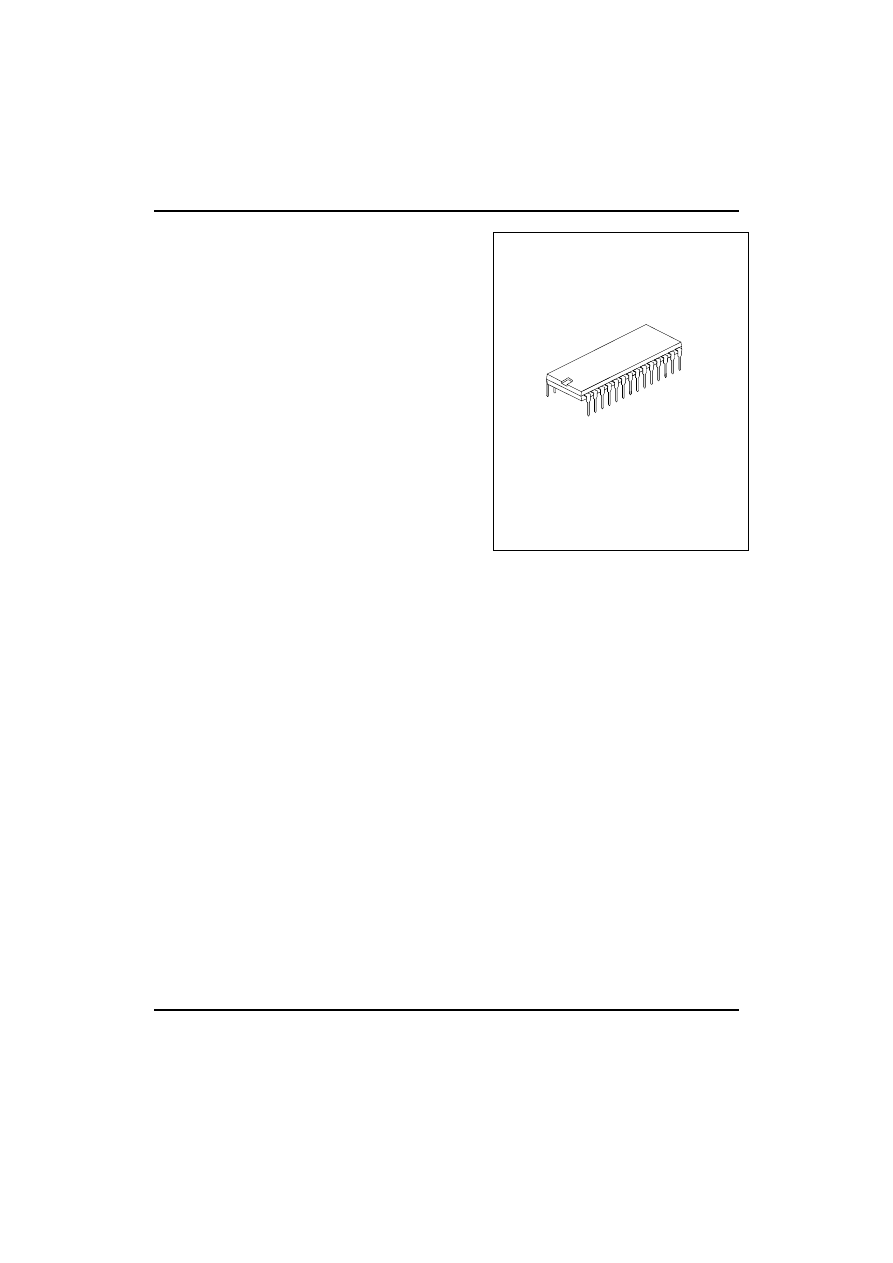
SDIP-28
UTC LM8560
MOS IC
UTC
UNISONIC TECHNOLOGIES CO., LTD.
2
QW-R502-005,D
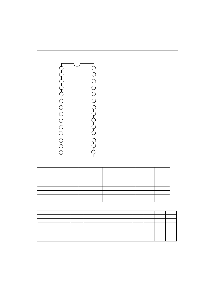
PIN CONFIGURATIONS
15
16
18
19
20
21
22
17
24
25
26
27
28
23
14
13
11
10
9
8
7
12
5
4
3
2
1
6
AM& 10'S HR
ag&de
PM& 10'S HR b
10'S HR c& HR e
HR b&g
HR c&d
HR a&f
MIN b&g
MIN c&d
MIN a&f
Colon Output
VSS
Sleep Output
Alarm OFF
Alarm Display
VDD
Hour Set
Minute Set
Sleep Display
Snooze Input
50/60 Hz Input
50/60 Hz Select
12/24 HR Select
CR Input
Alarm Output
LM8560
10'S MIN a&f
10'S MIN b&g
10'S MIN c&d
10'S MIN e &Min e
ABSOLUTE MAXIMUM RATINGS
(Ta=25
°C, Vss=0V)
PARAMETER SYMBOL
TEST
CONDITIONS
RATING
UNIT
Maximum Supply Voltage
V
DD (max)
-15~
+0.3
V
Input Voltage1
V
IN
1
50/60Hz Input
-15~ +0.3
V
Input Voltage2
V
IN
2
Except 50/60Hz Input
-15~ +0.3
V
Output Voltage
V
OUT
-15~
+0.3 V
Input Clamp Current
l
IN
50/60Hz Input
-0.4 ~+0.4
mA
Allowable Power Dissipation
P
D (max)
Ta=70
°C 700
mW
Operating Temperature
Topr
-30 ~ +70
°C
Storage Temperature
Tstg
-55 ~ +125
°C
ALLOWABLE OPERATING RANGES
(Ta=25
°C, Vss=0V )
PARAMETER SYMBOL
TEST
CONDITIONS
MIN.
TYP.
MAX.
UNIT
Supply Voltage
V
DD
-14
-7.5
V
Input “H” Level Voltage1
V
IH
1 50/60Hz
Input
-1
V
Input “L” Level Voltage1
V
IL
1 50/60Hz
Input
V
DD
+2 V
Input “H” Level Voltage2
V
IH
2
Except 50/60Hz Input
-1.5
V
Input “L” Level Voltage2
V
IL
2
Except 50/60Hz Input
V
DD
+2 V
50/60Hz Input Pin Input
Voltage
V
AC-IN
Sets
V
SS
as Reference
V
LED
V
UTC LM8560
MOS IC
UTC
UNISONIC TECHNOLOGIES CO., LTD.
3
QW-R502-005,D
ELECTRICAL CHARACTERISTICS
(Ta=25
°C, V
DD
=-12V unless otherwise specified)
PARAMETER SYMBOL
TEST
CONDITIONS
MIN.
TYP.
MAX.
UNIT
Input “H” Level Current 1
I
IH
1
50/60Hz Input, V
IN=
V
SS
10
µA
Input “L” Level Current 1
I
IL
1
50/60Hz Input, V
IN=
V
DD
10
µA
Input “H” Level Current 2
I
IH
2
Input Pins Other Than 50/60Hz Input
V
IN=
V
SS
20
µA
Input “L” Level Current 2
I
IL
2
Input Pins Other Than 50/60Hz Input
V
IN=
V
DD
10
µA
Output “H” Level Current 1
I
OH
1
Alarm Output and Sleep Output
V
OH
=V
SS
-1V
5 mA
Output Leakage Current 1
I
OF
1
Alarm Output and Sleep Output
V
OUT
=V
DD
10
µA
Output “H” Level Current 2
I
OH
2
AM & 10’S HR ag & de (24H mode)
V
OUT
=V
DD-
1V
36 mA
Output Leakage Current 2
I
OF
2
AM & 10’S HR ag & de (24H mode)
V
OUT
=V
DD
20
µA
Output “H” Level Current 3
I
OH
3
Segment Output Other Than Those
V
OUT
=V
SS
-1V
18 mA
Output Leakage Current 3
I
OF
3
Segment Output Other Than Those
Listed Above, V
OUT
=V
DD
20
µA
Power failure detection
Voltage
V
DD
-7.5 -5
V
Consumption Current
I
CC
Output set to off and Pull-down attached
input set open
5 7
mA
Backup Oscillator Stability
Factor
F
S
Standard
Value,900Hz,
V
DD
=-9V±10%-10
-10 10 %
Backup Oscillator
Accuracy
F
A
Standard Value,900Hz, V
DD
=-9V-10 -10 10 %
DESCRIPTION OF OPERATIONS
*50/60Hz Input:
Built-in Shumidt circuit enables noise eliminations at 50/60Hz commercial frequencies with use of a
simple CR filter. Built-in pull-up resistor.
*CR Input:
When the AC power supply is interrupted, the time counter switches to a holding state and a built-in
oscillator promptly begins operation. If 50/60Hz input continues for 3 clocks without arriving, this
oscillator’s output is activated and functions as the time counter clock in place of 50/60Hz input. The
frequency level of this clock oscillator is determined according to the CR value. While the above
mentioned oscillator is operating using backup mode, all segment output is switched to OFF.
(Note) When the backup oscillator is in use due to an AC power supply interruption, the 50/60Hz input
pin must be maintained open or at a V
SS
level.
*50/60 Selective Input:
When 50/60 selective input is connected to V
SS
, 50Hz use is enabled. When 50/60 selective input is
left open, VDD is activated using an internal pull-down resistor and the setting is switched to enable use
at 60Hz.
*Display Mode Selective Input (Alarm Select/Sleep Select):
Since the pull-down resistor is built-in , selection from four display modes is possible using two SPST
switches (single-pole and single-throw switches). Table 1 shows these display mode selections.
UTC LM8560
MOS IC
UTC
UNISONIC TECHNOLOGIES CO., LTD.
4
QW-R502-005,D
Table1 Display Modes
Selective lnput
Alarm Sleep
Display Mode
Digit No. 1
Digit No. 2
Digit No. 3
Digit No.4
NC NC
Time
display
10’s place for
hour, AM/PM
Hour
10’s place for
Minute
Minute
V
SS
NC
Alarm
display
10’s place for
hour, AM/PM
Hour
10’s place for
Minute
Minute
NC V
SS
Sleep
display Clear
Hour
10’s place for
Minute
Minute
V
SS
V
SS
Second
display
Clear
Minute
10”s place for
Second
Second
Note: Activating V
SS
using two inputs simultaneously (alarm select and sleep select), the display mode is switched to
display seconds.
*Time Setting Input:
There are two setting inputs for use with “hour” and “minute”. Time content settings show in Table2 are
possible by activating V
SS
to these pins, A pull-down resistor is built-in.
Table2 Setting contents
Display Mode
Set Input
Functions
Hour
Immediately adds 1 to hour digits and then assigns an additional 1, at a
speed of 2 Hz, after each 1/4 to 3/4 second.
Min
Immediately adds 1 to minute digits and then assigns an additional 1, at a
speed of 2 Hz, after each 1/4 to 3/4 second. Seconds are rest.
Time
Both
Operates both as outline above.
Hour (note1)
Second digits are cleared to [00].
Min Time
holds.
Second
(Alarm & Sleep)
Both (note2)
Resets hour and minute digits as [0:00] when operating in 24-H mode or
[12:00] when operating in 12-H mode.
Hour
Immediately adds 1 to hour digits and then assigns an additional 1, at a
speed of 2 Hz, after each 1/4 to 3/4 second.
Min
Immediately adds 1 to minute digits and then assigns an additional 1, at a
speed of 2 Hz, after each 1/4 to 3/4 second.
Alarm
Both
Resets hour and minute digits as [0:00] when operating in 24-hour mode or
[12:00] when operating in 12-hour mode.
-
Sets sleep counter to [0:59] instantly when V
DD
is activated to sleep select
Hour
Sets Sleep counter to [1:59] instantly when V
DD
is activated to sleep select
and hour at the same time.
Min
Sleep counter looses 1 at a speed of 2 Hz.
Sleep
Both
Sleep counter looses 1 at a speed of 2 Hz.
Note:1.Once conditions have been switched to reset or hold, input of other functions is locked until both Hour and
Min input have been separated.
2.When the digital reading for seconds is between 30 and 59 seconds, 1 is added to the digits for minutes as
he digital reading for seconds rests to [00].
*12/24H Select Input :
When this pin set open (V
DD
), a 12-hour display is enabled whereas connecting this pin to V
SS
enables
the 24-hour display. A pull-down resistor is build-in.
*Power Failure Detection Display :

UTC LM8560
MOS IC
UTC
UNISONIC TECHNOLOGIES CO., LTD.
5
QW-R502-005,D
When activated by drop in power supply, all segments which are lit begin to blink and the unit switches
to a power failure detection display. The power failure detection display is canceled by activating V
SS
to
Hours set or Min set.
*Alarm Operation and Alarm Output :
The alarm signal outputs when alarm content matches the content of current time. When not rest by
either snooze input or alarm off input, output continues after 1 hour and 59 minutes. This output signal
consists of 900Hz 2Hz intermittent (50% duty) modulation signals, When the need arises , a filter can be
applied to after the alarm signal to a DC signal.
*Snooze Input :
When the alarm is sounding and instantly activating V
SS
to this pin , alarm output is set to OFF for a
period between 8 and 9 minutes after which time the alarm signal is once again output. The snooze
function can be used repeatedly in 1 hours and 59 minutes intervals. A pull-down resistor is built-in
Activating V
SS
to the snooze pin when the alarm is OFF resets the sleep timer counter to [0:00 ](This is
known as the one-touch sleep timer reset function.)
*Alarm Off Input :
Activating this input pin to VSS instantly sets alarm output to OFF.A pull-down resistor is built-in.
*Sleep Timer and Sleep Output :
Sleep output can turn on the radio and can be set for time intervals of 59 minutes or 1 hour and 59
minute. Refer to Table 2 for the proper selection procedure (59 minutes or 1 hour and 59 minute
selection.) This sleep timer is constructed using a down counter and when the counter content arrives at
[00], output is set to off and the radio turns off. Adding V
SS
to snooze input turns sleep output off. When
sleep output is on.
UTC LM8560
MOS IC
UTC
UNISONIC TECHNOLOGIES CO., LTD.
6
QW-R502-005,D
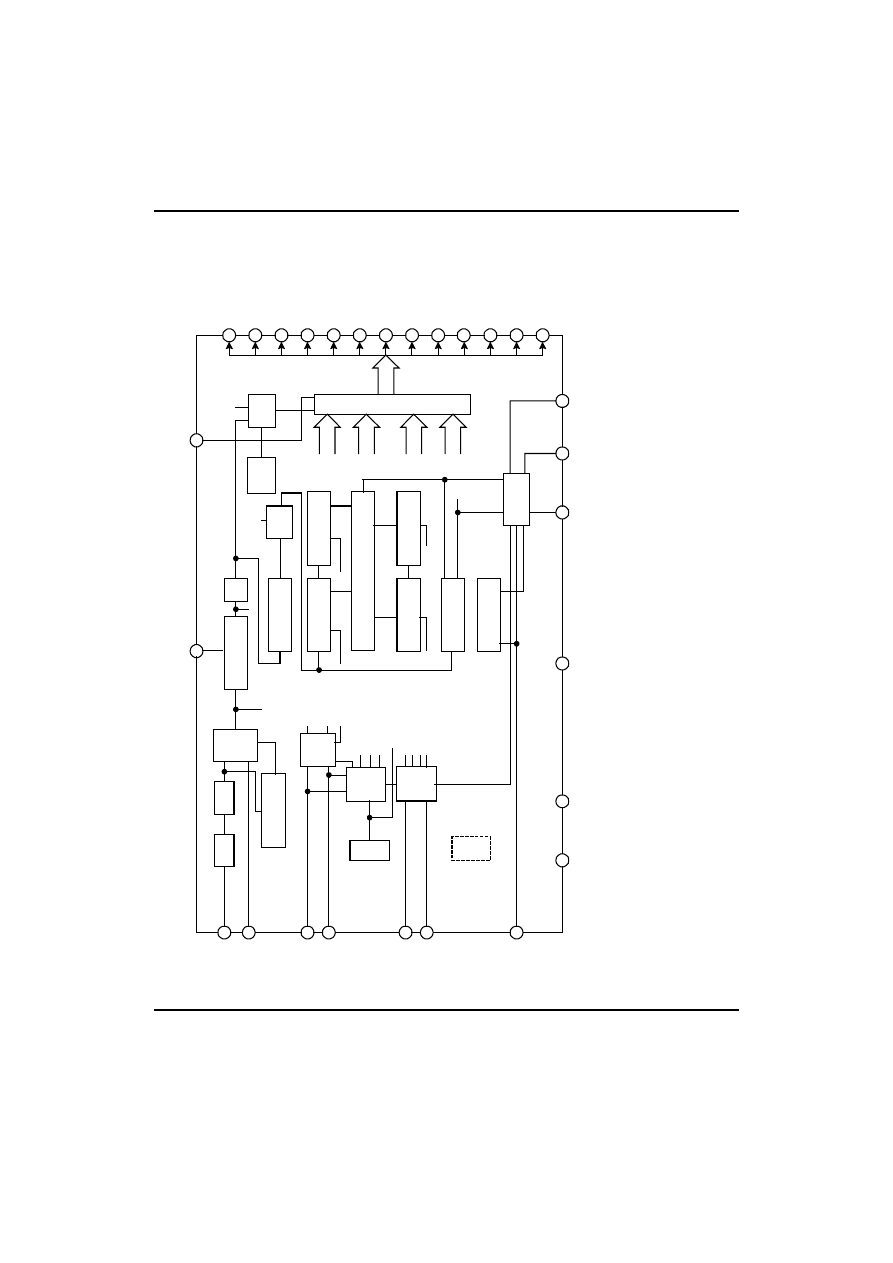
BLOCK DIAGRAM
22
21
20
18
17
15
27
26
25
28
2
4
7
8
9
10
11
12
13
14
5
6
3
1
16
19
23
24
Output Decoder/Driver
Bl
a
nk&
Fl
as
h
PF
.
DET
AM&10
'S
HR a
g&d
e
PM&1
0'S HR b
10
'S
HR c
&
HRe
HR b
&
g
HR c
&
d
HR
a&f
10
'S M
IN
a&
f
10
'S
M
IN
b
&
g
10
'S
M
IN
c
&
d
1
0'
S
MIN
e&Min e
MIN b
&
g
MIN c&d
MIN a
&
f
12
/2
4
HR
Se
le
ct
50
/60
Hz
Se
le
ct
50
/6
0
Hz
Se
c
Ti
me
Alar
m
Sl
e
ep
Sl
e
ep
Ou
tpu
t
Al
a
rm
Ou
tpu
t
Al
a
rm
OF
F
Co
lo
n
Ou
tp
ut
VSS
VD
D
Sno
oze
In
pu
t
Sl
ee
p Displ
ay
A
lar
m
D
is
pl
ay
H
our
S
e
t
M
inu
te
Se
t
50
/6
0H
z I
nput
C
R
In
pu
t
GATE
TDi
sp &
S.
Samp
le
1Hz
2H
z
1/
2
1/
25
or
1/3
0
50
/60
H
z
GAT
E
CTR
OSC
To
ne
S
tan
db
y D
E
T
In
pu
t
Con
tro
l
S.
S
a
m
p
le
F.S
amp
le
2H
z
Sec
RS
TYHL
D
T.
R
S
T
AL
.RS
T
PWR UP
SEC Disp
T
Di
sp
AL Di
sp
SL
D
is
p
Re
se
t
Co
ntr
ol
Dis
p
la
y
Co
ntro
l
PWR UP
Second
Display
SEC
CT
R
T
ime
HR.CT
R
Time min.CT
R
T
im
e
&S.
Samp
le
T
ime
&F.S
ampl
e
Comp
ara
tor
Al
a
rm MIN
CT
R
Ala
rm HR C
T
R
Al
ar
m
&
F
.Sa
m
pl
e
Ti
m
e
&
F
.S
amp
le
S
lee
p CTR
Co
ntro
l
PW
R
UP
Ou
tp
ut
Con
tro
l
UTC LM8560
MOS IC
UTC
UNISONIC TECHNOLOGIES CO., LTD.
7
QW-R502-005,D
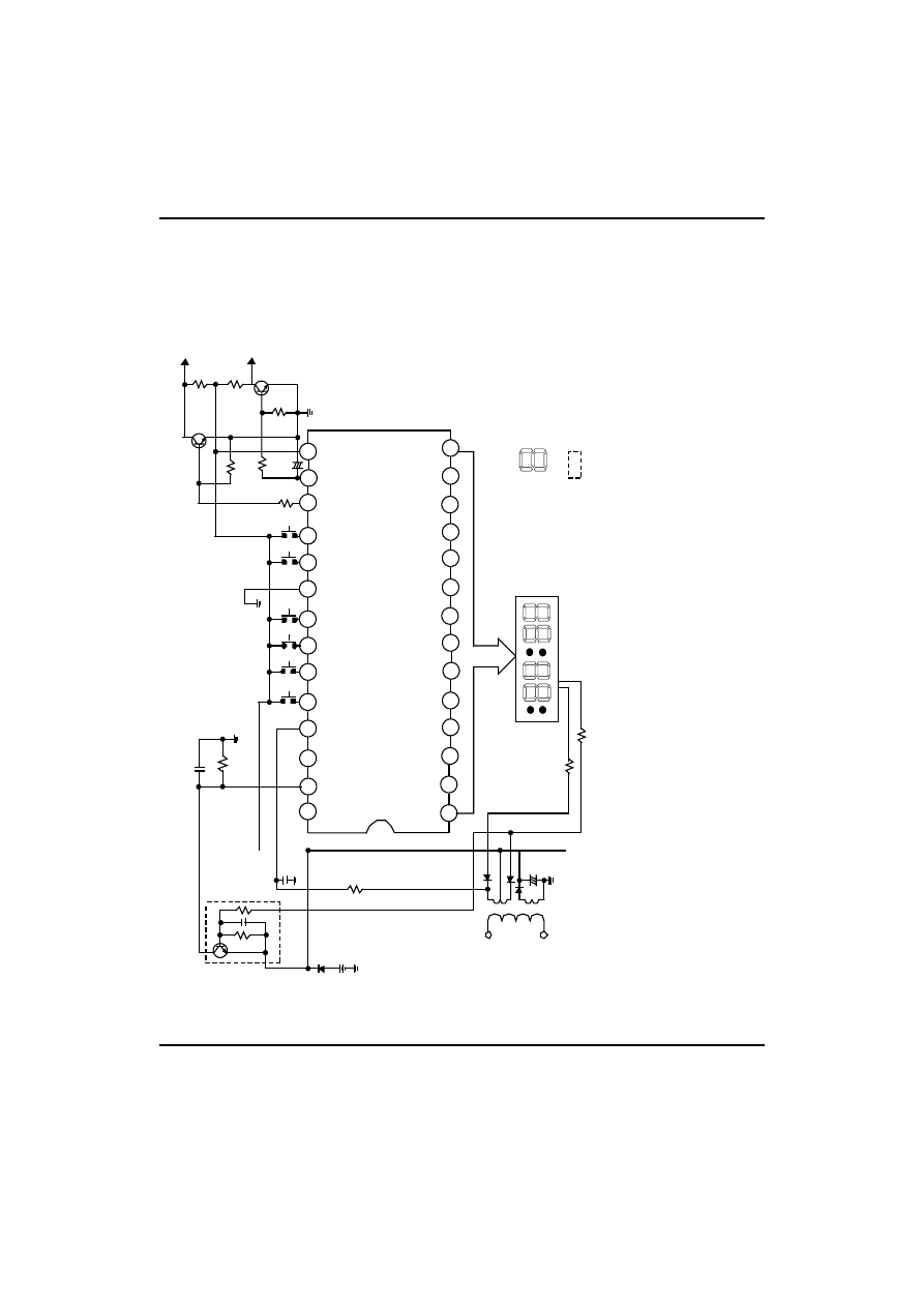
CLOCK-RADIO APPLICATION CIRCUIT (Positive Power Supply)
28
12 H
R
NC
60 H
Z
NC
Ba
ckup
Ba
tter
y
AC
100k
cycle 1
cycle 2
R1
110
k
C1
0.015
μ
f=
900H
z
2.2k
2.2k
4.7k
27k
27k
4.7k
No
te
:
2
1
D
upl
ex
LED
Cathode
C
o
mmo
n
12 Ho
ur Displa
y and 60H
z Circuit
Diagram
+
0.001
μ
U
n
it(resistor:
Ω
, capaci
tor
: F)
15
16
18
19
20
21
22
17
24
25
26
27
23
14
13
11
10
9
8
7
12
5
4
3
2
1
6
VSS
Sleep
O
utput
Al
ar
m
OFF
Alar
m
Di
sp
la
y
VD
D
H
our
Se
t
Minute
Set
Sleep
Di
sp
la
y
Snoo
ze
Inpu
t
50/60
Hz
Input
50/60
Hz
Selec
t
12/24
HR
Selec
t
CR
Input
Alar
m
O
utput
AM&
10'S
HR
ag&de
PM&
10'S
HR b
10'S
HR c
&
HR e
HR
b&g
HR
c&
d
HR
a&f
10'
S
MI
N
a&
f
10'S
MIN
b&g
10
'S
MI
N
c&d
10'S
MIN e
&Min e
MIN
b&g
MIN
c&
d
MIN
a&f
Col
on
O
utput
Thi
s ci
rc
ui
t i
s used as n
o
is
e i
n
ter
fer
e
n
ce str
ipper for
the LW
ban
d.(
B
ackup c
o
ntr
o
l i
s ena
lbl
ed except
for
batter
y b
a
ckup m
ode
LM8560
+
μ
0.47
a
b
c
d
e
f
g
UTC LM8560
MOS IC
UTC
UNISONIC TECHNOLOGIES CO., LTD.
8
QW-R502-005,D
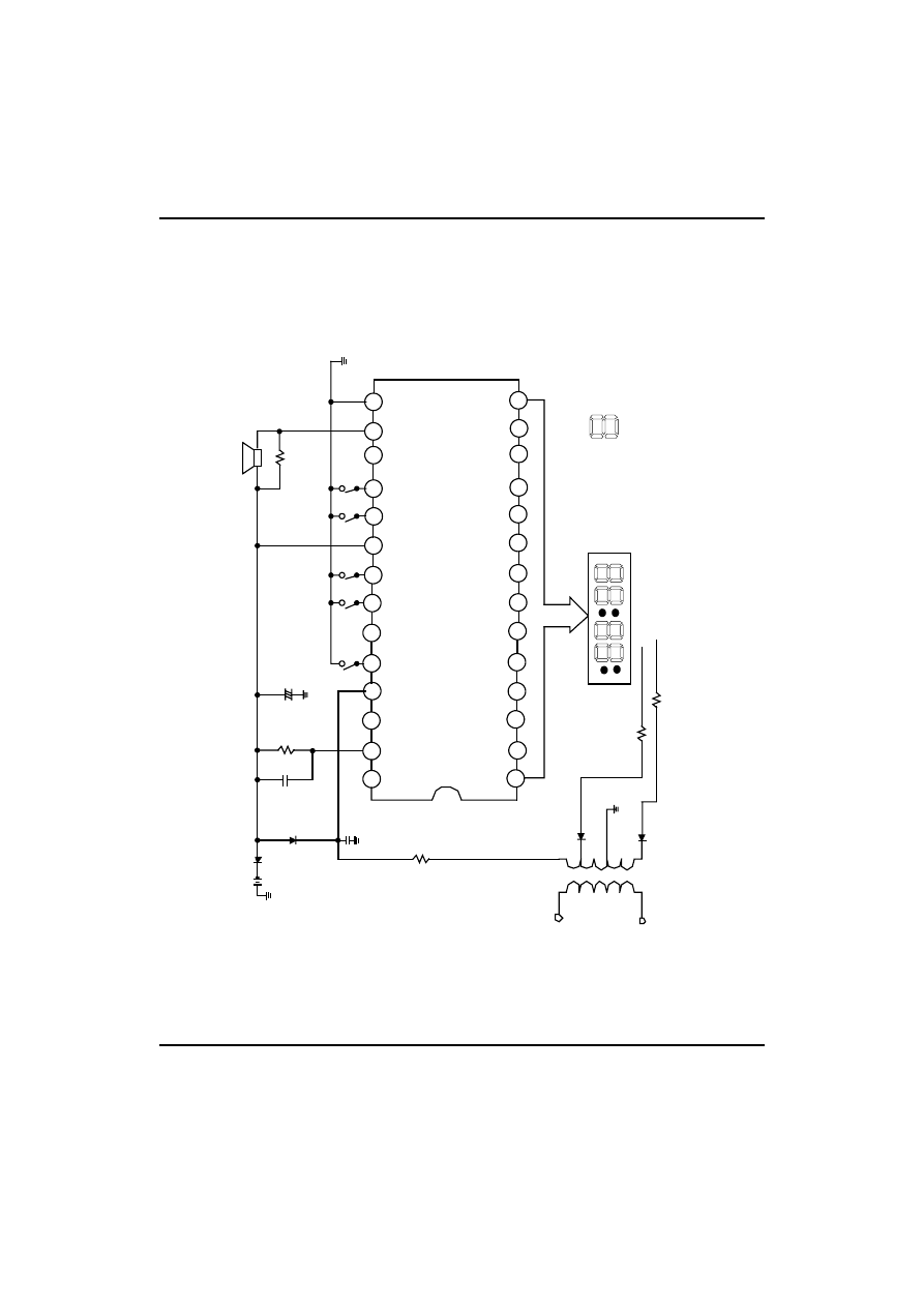
CLOCK APPLICATION CIRCUIT (Negative Power Supply)
15
16
18
19
20
21
22
17
24
25
26
27
28
23
14
13
11
10
9
8
7
12
5
4
3
2
1
6
AM
&
10'
S
HR
PM&
10'S
HR
b
10'
S
HR
c
&
HR e
HR
b&
g
HR
c&
d
HR
a&
f
10'
S
MIN
a&
f
10'
S
MIN
b&g
10'
S
MIN
c&
d
10
'S
MIN
e
&M
in
e
MIN
b&
g
MIN
c&
d
MIN
a&
f
Colon
O
utput
VS
S
S
leep
O
utput
Alarm
OF
F
Al
ar
m
Dis
play
VD
D
H
our
Se
t
Minute
Se
t
Sleep
Di
sp
la
y
Sn
o
oz
e
Input
50/60
Hz
Input
50/60
Hz
Se
le
ct
1
2/24
HR
Selec
t
CR
In
put
12
H
R
NC
60
H
Z
NC
AC
0.
00
1μ
100
k
cy
cle
1
cyc
le 2
R1
11
0k
f=
900
H
z
C1
No
te
:
2.
1.
W
h
en
Ba
tte
ry
b
ack
up
o
r
ton
e
ou
tp
ut
is
no
t
us
ed
,C
R
in
pu
t i
s co
nn
ec
ed
t
o
V
ss
Ca
th
od
e
C
ommo
n
12
H
ou
r
D
is
pl
ay
an
d 60
Hz
Ci
rc
uit
Di
agra
m
Piezo
Buzz
er
0.
01
5
μ
33
0
μ
+
Al
ar
m
Ou
tp
ut
U
nit
(r
esis
to
r:
Ω
, ca
pa
cito
r
: F)
LM
8560
Du
pl
ex
LE
D
a
b
c
d
e
f
g
Wyszukiwarka
Podobne podstrony:
IS LM
interpretacja IS LM
IS LM pelny model
AIWA LM 99
LM inżynier środowiska
LM Pracuj spec Analityk finansowy
LM Pracuj spec Referent
Protokół, praca - kadry, płace, lm, rozmowa kwalifikacyjna, Materiały do zorganizowania obozu lub ko
LM & L, AR Poznań - Leśnictwo, szkółkarstwo
LM Pracuj spec Programista
MwE 1 3 2005 lm
is lm
ŁM gos wod cw1 p2
lm ksiegowa, Wzory dokumentów, Listy motywacyjne
Makroekonomia - model IS-LM, Studia
WZÓR LISTU MOTYWACYJNEGO (LM) DLA KIEROWNIKA BUDOWY, List Motywacyjny
lm(ap)
LM inzynier procesu
więcej podobnych podstron