
a
ADSP-21469 EZ-Board
®
Evaluation System Manual
Revision 1.1, July 2012
Part Number
82-000221-01
Analog Devices, Inc.
One Technology Way
Norwood, Mass. 02062-9106

Copyright Information
© 2012 Analog Devices, Inc., ALL RIGHTS RESERVED. This docu-
ment may not be reproduced in any form without prior, express written
consent from Analog Devices, Inc.
Printed in the USA.
Disclaimer
Analog Devices, Inc. reserves the right to change this product without
prior notice. Information furnished by Analog Devices is believed to be
accurate and reliable. However, no responsibility is assumed by Analog
Devices for its use; nor for any infringement of patents or other rights of
third parties which may result from its use. No license is granted by impli-
cation or otherwise under the patent rights of Analog Devices, Inc.
Trademark and Service Mark Notice
The Analog Devices logo, CrossCore, EngineerZone, EZ-Extender,
EZ-KIT Lite, SHARC, and VisualDSP++ are registered trademarks of
Analog Devices, Inc.
All other brand and product names are trademarks or service marks of
their respective owners.

Regulatory Compliance
The ADSP-21469 EZ-Board is designed to be used solely in a laboratory
environment. The board is not intended for use as a consumer end prod-
uct or as a portion of a consumer end product. The board is an open
system design which does not include a shielded enclosure and therefore
may cause interference to other electrical devices in close proximity. This
board should not be used in or near any medical equipment or RF devices.
The ADSP-21469 EZ-Board has been certified to comply with the essen-
tial requirements of the European EMC directive 2004/108/EC and
therefore carries the “CE” mark.
The ADSP-21469 EZ-Board has been appended to Analog Devices, Inc.
EMC Technical File (EMC TF) referenced DSPTOOLS1, issue 2 dated
June 4, 2008 and was declared CE compliant by an appointed Notified
Body (No.0673) as listed below.
Notified Body Statement of Compliance: Z600ANA2.033, dated May
2009.
Issued by: Technology International (Europe) Limited
60 Shrivenham Hundred Business Park
Shrivenham, Swindon, SN6 8TY, UK
The EZ-Board evaluation system contains ESD (electrostatic discharge)
sensitive devices. Electrostatic charges readily accumulate on the human
body and equipment and can discharge without detection. Permanent
damage may occur on devices subjected to high-energy discharges. Proper
ESD precautions are recommended to avoid performance degradation or
loss of functionality. Store unused EZ-Board boards in the protective ship-
ping package.


ADSP-21469 EZ-Board Evaluation System Manual
v
CONTENTS
Product Overview ........................................................................ xii
Purpose of This Manual ................................................................ xv
Intended Audience ........................................................................ xv
Manual Contents .......................................................................... xv
What’s New in This Manual ......................................................... xvi
Technical Support ........................................................................ xvi
Supported Processors ................................................................... xvii
Product Information .................................................................. xviii
Analog Devices Web Site ...................................................... xviii
EngineerZone ......................................................................... xix
Related Documents ...................................................................... xix
Notation Conventions ................................................................... xx
Package Contents .......................................................................... 1-2
Default Configuration ................................................................... 1-3
CCES Install and Session Startup .................................................. 1-5
Session Startup ........................................................................ 1-6

Contents
vi
ADSP-21469 EZ-Board Evaluation System Manual
VisualDSP++ Install and Session Startup ....................................... 1-9
Session Startup ...................................................................... 1-10
CCES Evaluation License ........................................................... 1-11
VisualDSP++ Evaluation License ................................................. 1-12
Memory Map ............................................................................. 1-13
DDR2 Interface ......................................................................... 1-14
Parallel Flash Memory Interface .................................................. 1-15
SPI Interface .............................................................................. 1-16
Link Port Interface ..................................................................... 1-16
Temperature Sensor Interface ...................................................... 1-17
S/PDIF Interface ........................................................................ 1-18
Audio Interface ........................................................................... 1-19
UART Interface .......................................................................... 1-20
LEDs and Push Buttons .............................................................. 1-21
JTAG Interface ........................................................................... 1-23
Land Grid Array ......................................................................... 1-24
Expansion Interface II ................................................................. 1-25
Power Measurements .................................................................. 1-26
Power-On-Self Test ..................................................................... 1-26
Example Programs ...................................................................... 1-27
Board Design Database ............................................................... 1-27

ADSP-21469 EZ-Board Evaluation System Manual
vii
Contents
ADSP-21469 EZ-BOARD HARDWARE REFERENCE
System Architecture ...................................................................... 2-2
DAI Interface .......................................................................... 2-3
DPI Interface .......................................................................... 2-4
Flags and Memory Selects .............................................................. 2-5
Push Button and Switch Settings ................................................... 2-7
DAI [1–8] Enable Switch (SW1) .............................................. 2-8
DAI [9–16] Enable Switch (SW2) ............................................ 2-8
DPI [1–8] Enable Switch (SW3) .............................................. 2-9
Boot Mode Select Switch (SW4) ............................................ 2-10
DSP Clock Configuration Switch (SW5) ................................ 2-11
DAI [17–20] Enable Switch (SW7) ........................................ 2-11
Programmable Flag Push Buttons (SW8–11) .......................... 2-12
Reset Push Button (SW12) .................................................... 2-12
Asynchronous Control Enable Switch (SW13) ........................ 2-13
DPI [9–14] Enable Switch (SW14) ........................................ 2-13
Audio In1 Left Selection Switch (SW15) ................................ 2-14
Audio In1 Right Selection Switch (SW16) .............................. 2-15
Audio In2 Right Selection Switch (SW17) .............................. 2-15
Audio In2 Left Selection Switch (SW18) ................................ 2-16
JTAG Switches (SW19–22) .................................................... 2-17
Headphone Enable Switch (SW23) ........................................ 2-19
Audio Loopback Switches (SW24–25) ................................... 2-19

Contents
viii
ADSP-21469 EZ-Board Evaluation System Manual
Jumpers ...................................................................................... 2-20
Flash WP Jumper (JP1) ......................................................... 2-21
S/PDIF Loopback Jumper (JP2) ............................................ 2-21
UART RTS/CTS Jumper (JP3) ............................................. 2-21
UART Loopback Jumper (JP4) .............................................. 2-21
LEDs ......................................................................................... 2-22
GPIO LEDs (LED1–8) ......................................................... 2-23
Power LED (LED9) .............................................................. 2-23
Reset LED (LED10) ............................................................. 2-23
Thermal Limit LED (LED11) ............................................... 2-24
Connectors ................................................................................. 2-25
Expansion Interface II Connector (J1) ................................... 2-26
RS-232 Connector (J2) ......................................................... 2-26
Link Port 1 Connector (J3) ................................................... 2-26
RCA Audio Connector (J4) ................................................... 2-27
RCA Audio Connector (J5) ................................................... 2-27
S/PDIF IN Connector (J6) .................................................... 2-27
S/PDIF OUT Connector (J7) ............................................... 2-27
Headphone Out Connector (J8) ............................................ 2-28
JTAG Connector (P1) ........................................................... 2-28
Expansion Interface II Connector (P2) .................................. 2-28
DMAX Land Grid Array Connectors (P5–7) ......................... 2-29
Differential In/Out Connectors (P8–9) .................................. 2-29
MLB Connector (P10) .......................................................... 2-29

ADSP-21469 EZ-Board Evaluation System Manual
ix
Contents
Link Port 0 Connector (P12) ................................................. 2-30
VDD_DDR2 Power Connector (P13) .................................... 2-30
VDDINT Power Connector (P14) ......................................... 2-30
VDDEXT Power Connector (P15) ......................................... 2-30
Power Connector (P16) ......................................................... 2-31
Standalone Debug Agent Connector (ZP1) ............................ 2-31

Contents
x
ADSP-21469 EZ-Board Evaluation System Manual

ADSP-21469 EZ-Board Evaluation System Manual
xi
PREFACE
Thank you for purchasing the ADSP-21469 EZ-Board
®
, Analog Devices,
Inc. evaluation system for SHARC
®
processors.
SHARC processors are based on a 32-bit super Harvard architecture that
includes a unique memory architecture comprised of two large on-chip,
dual-ported SRAM blocks coupled with a sophisticated IO processor,
which gives a SHARC processor the bandwidth for sustained high-speed
computations. SHARC processors represents today’s de facto standard for
floating-point processing, targeted toward premium audio applications.
The evaluation board is designed to be used in conjunction with the
CrossCore
®
Embedded Studio (CCES) and VisualDSP++
®
development
environments to test the capabilities of the ADSP-21469 SHARC proces-
sors. The development environment aids advanced application code
development and debug, such as:
• Create, compile, assemble, and link application programs written
in C++, C, and ADSP-21469 assembly
• Load, run, step, halt, and set breakpoints in application programs
• Read and write data and program memory
• Read and write core and peripheral registers
• Plot memory
Access to the ADSP-21469 processor from a personal computer (PC) is
achieved through a USB port or an external JTAG emulator. The USB
interface of the standalone debug agent gives unrestricted access to the

Product Overview
xii
ADSP-21469 EZ-Board Evaluation System Manual
ADSP-21469 processor and evaluation board’s peripherals. Analog
Devices JTAG emulators offer faster communication between the host PC
and target hardware. To learn more about Analog Devices emulators and
processor development tools, go to
http://www.analog.com/dsp/tools
.
The ADSP-21469 EZ-Board provides example programs to demonstrate
the capabilities of the product.
Product Overview
The board features:
• Analog Devices ADSP-21469 SHARC processor
• Core performance up to 450 MHz
• 324-pin PBGA package
• 25 MHz oscillator
• 5 Mb of internal RAM memory
• Double data rate synchronous dynamic random access memory
(DDR2)
• Micron MT47H64M16HR-3 – 128 MB (64M x 16 bits)
• Performance of up to 225 MHz clock rate
• Parallel flash memory
• Numonyx M29W320EB – 4 MB (4M x 8 bits)

ADSP-21469 EZ-Board Evaluation System Manual
xiii
Preface
• SPI flash memory
• Numonyx M25P16 – 16 Mb
• Analog audio interface
• Analog Devices AD1939 audio codec
• Eight DAC outputs for four channels of stereo output
• Four ADC inputs for two channels of stereo input
• Two DB25 connectors for differential inputs/outputs
• 3.5 mm headphone jack with volume control connected to
one of the stereo outputs
• Supports all eight DACs and four ADCs in TDM and I
2
S
modes at 48 KHz, 96 KHz, and 192 KHz sample rates
• Digital audio interface (S/PDIF)
• RCA phono jack output
• RCA phono jack input
• Link port interface
• Two Samtec ERF8/ERM8 series connectors
• Link ports performance up to 166 MHz
• Two EZ-Boards can mate with no cables required
• Temperature monitor
• ON Semiconductor ADM1032
• Local and remote temperature sensing

Product Overview
xiv
ADSP-21469 EZ-Board Evaluation System Manual
• Universal asynchronous receiver/transmitter (UART)
• ADM3202 RS-232 line driver/receiver
• DB9 female connector
• LEDs
• Eleven LEDs: one board reset (red), eight general-purpose
(amber), one temperature sensor LED (amber), and one
power (green)
• Push buttons
• Five push buttons: one reset, two connected to DAI, two
connected to
FLAG
pins of the processor
• Expansion interface II
• Next generation of the expansion interface design, provides
access to most of the ADSP-21469 processor signals
• Land grid array
• Easy probing of all port pins and most asynchronous
memory interface (AMI) signals
• Other features
• JTAG ICE 14-pin header
• SHARC power measurement jumpers
Please visit
for additional information,
including CCES support.
For information about the hardware components of the EZ-Board, refer
to
“ADSP-21469 EZ-Board Hardware Reference” on page 2-1
.

ADSP-21469 EZ-Board Evaluation System Manual
xv
Preface
Purpose of This Manual
The ADSP-21469 EZ-Board Evaluation System Manual provides instruc-
tions for installing the product hardware (board). The text describes
operation and configuration of the board components and provides
guidelines for running your own code on the ADSP-21469 EZ-Board.
Finally, a schematic and a bill of materials are provided for reference.
Intended Audience
The primary audience for this manual is a programmer who is familiar
with Analog Devices processors. This manual assumes that the audience
has a working knowledge of the appropriate processor architecture and
instruction set.
Programmers who are unfamiliar with Analog Devices processors can use
this manual, but should supplement it with other texts that describe your
target architecture. For the locations of these documents, see
.
Programmers who are unfamiliar with CCES or VisualDSP++ should refer
to the online help and user’s manuals.
Manual Contents
The manual consists of:
• Chapter 1,
“Using the ADSP-21469 EZ-Board” on page 1-1
Describes EZ-Board functionality from a programmer’s perspective
and provides an easy-to-access memory map.
• Chapter 2,
“ADSP-21469 EZ-Board Hardware Reference” on
Provides information on the EZ-Board hardware components.

What’s New in This Manual
xvi
ADSP-21469 EZ-Board Evaluation System Manual
• Appendix A,
“ADSP-21469 EZ-Board Bill Of Materials” on
Provides a list of components used to manufacture the EZ-Board.
• Appendix B,
“ADSP-21469 EZ-Board Schematic” on page B-1
Provides the resources to allow EZ-Board board-level debugging or
to use as a reference guide. Appendix B is part of the online help.
What’s New in This Manual
This is revision 1.1 of the ADSP-21469 EZ-Board Evaluation System Man-
ual. The manual has been updated to include CCES information.
For the latest version of this manual, please refer to the Analog Devices
Web site.
Technical Support
You can reach Analog Devices processors and DSP technical support in
the following ways:
• Post your questions in the processors and DSP support community
at EngineerZone
®
:
http://ez.analog.com/community/dsp
• Submit your questions to technical support directly at:

ADSP-21469 EZ-Board Evaluation System Manual
xvii
Preface
• E-mail your questions about processors, DSPs, and tools develop-
ment software from CrossCore Embedded Studio or
VisualDSP++:
Choose Help > Email Support. This creates an e-mail to
processor.tools.support@analog.com
and automatically attaches
your CrossCore Embedded Studio or VisualDSP++ version infor-
mation and
license.dat
file.
• E-mail your questions about processors and processor applications
to:
or
• In the USA only, call 1-800-ANALOGD (1-800-262-5643)
• Contact your Analog Devices sales office or authorized distributor.
Locate one at:
• Send questions by mail to:
Processors and DSP Technical Support
Analog Devices, Inc.
Three Technology Way
P.O. Box 9106
Norwood, MA 02062-9106
USA
Supported Processors
This evaluation system supports Analog Devices ADSP-21462,
ADSP-21465, ADSP-21467, and ADSP-21469 SHARC processors.

Product Information
xviii
ADSP-21469 EZ-Board Evaluation System Manual
Product Information
Product information can be obtained from the Analog Devices Web site
and the online help system.
Analog Devices Web Site
The Analog Devices Web site,
, provides information
about a broad range of products—analog integrated circuits, amplifiers,
converters, and digital signal processors.
To access a complete technical library for each processor family, go to
http://www.analog.com/processors/technical_library
selection opens a list of current manuals related to the product as well as a
link to the previous revisions of the manuals. When locating your manual
title, note a possible errata check mark next to the title that leads to the
current correction report against the manual.
is a free feature of the Analog Devices Web site that
allows customization of a Web page to display only the latest information
about products you are interested in. You can choose to receive weekly
e-mail notifications containing updates to the Web pages that meet your
interests, including documentation errata against all manuals.
provides access to books, application notes, data sheets, code
examples, and more.
(found on the Analog Devices home page) to sign up. If
you are a registered user, just log on. Your user name is your e-mail
address.

ADSP-21469 EZ-Board Evaluation System Manual
xix
Preface
EngineerZone
EngineerZone is a technical support forum from Analog Devices. It allows
you direct access to ADI technical support engineers. You can search
FAQs and technical information to get quick answers to your embedded
processing and DSP design questions.
Use EngineerZone to connect with other DSP developers who face similar
design challenges. You can also use this open forum to share knowledge
and collaborate with the ADI support team and your peers. Visit
to sign up.
Related Documents
For additional information about the product, refer to the following
publications.
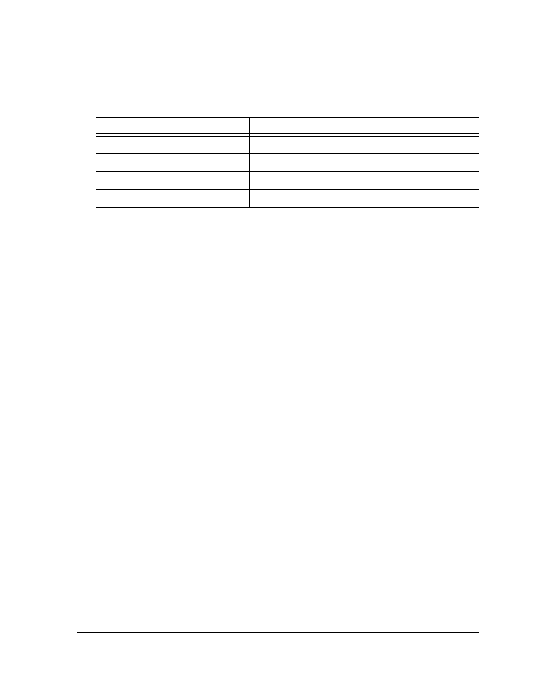
Table 1. Related Processor Publications
Title
Description
ADSP-21467/ADSP-21469 SHARC Processor Data
Sheet
General functional description, pinout, and
timing of the processor
ADSP-214xx SHARC Processor Hardware Reference Description of the internal processor archi-
tecture, registers, and all peripheral functions
SHARC Processor Programming Reference
Description of all allowed processor assembly
instructions

Notation Conventions
xx
ADSP-21469 EZ-Board Evaluation System Manual
Notation Conventions
Text conventions used in this manual are identified and described as
follows.
Example
Description
Close command
(File menu)
Titles in reference sections indicate the location of an item within the
development environment’s menu system (for example, the Close com-
mand appears on the File menu).
{this | that}
Alternative required items in syntax descriptions appear within curly
brackets and separated by vertical bars; read the example as
this
or
that
. One or the other is required.
[this | that]
Optional items in syntax descriptions appear within brackets and sepa-
rated by vertical bars; read the example as an optional
this
or
that
.
[this,…]
Optional item lists in syntax descriptions appear within brackets delim-
ited by commas and terminated with an ellipse; read the example as an
optional comma-separated list of
this
.
.
SECTION
Commands, directives, keywords, and feature names are in text with
letter gothic
font.
filename
Non-keyword placeholders appear in text with italic style format.
Note: For correct operation, ...
A Note provides supplementary information on a related topic. In the
online version of this book, the word Note appears instead of this
symbol.
Caution: Incorrect device operation may result if ...
Caution: Device damage may result if ...
A Caution identifies conditions or inappropriate usage of the product
that could lead to undesirable results or product damage. In the online
version of this book, the word Caution appears instead of this symbol.
Warning: Injury to device users may result if ...
A Warning identifies conditions or inappropriate usage of the product
that could lead to conditions that are potentially hazardous for the
devices users. In the online version of this book, the word Warning
appears instead of this symbol.

ADSP-21469 EZ-Board Evaluation System Manual
1-1
1 USING THE ADSP-21469
EZ-BOARD
This chapter provides specific information to assist you with development
of programs for the ADSP-21469 EZ-Board evaluation system.
The following topics are covered.
•
“Package Contents” on page 1-2
•
“Default Configuration” on page 1-3
•
“CCES Install and Session Startup” on page 1-5
•
“VisualDSP++ Install and Session Startup” on page 1-9
•
“CCES Evaluation License” on page 1-11
•
“VisualDSP++ Evaluation License” on page 1-12
•
•
•
“Parallel Flash Memory Interface” on page 1-15
•
•
“Link Port Interface” on page 1-16
•
“Temperature Sensor Interface” on page 1-17
•
“S/PDIF Interface” on page 1-18
•

Package Contents
1-2
ADSP-21469 EZ-Board Evaluation System Manual
•
•
“LEDs and Push Buttons” on page 1-21
•
•
“Land Grid Array” on page 1-24
•
“Expansion Interface II” on page 1-25
•
“Power Measurements” on page 1-26
•
“Power-On-Self Test” on page 1-26
•
“Example Programs” on page 1-27
•
“Board Design Database” on page 1-27
For information on the graphical user interface, including the boot load-
ing, target options, and other facilities, refer to the online help.
For more information about the ADSP-21469 SHARC processor, see doc-
uments referenced in
.
Package Contents
Your ADSP-21469 EZ-Board evaluation system package contains the fol-
lowing items.
• ADSP-21469 EZ-Board
• Universal 5.0V DC power supply
• 3.5 mm stereo headphones
• 6-foot RCA audio cable
ADSP-21469 EZ-Board Evaluation System Manual
1-3
Using the ADSP-21469 EZ-Board
• 6-foot 3.5 mm/RCA x 2 Y-cable
• 3.5 mm stereo female to RCA male Y-cable
If any item is missing, contact the vendor where you purchased your
EZ-Board or contact Analog Devices, Inc.
Default Configuration
The ADSP-21469 EZ-Board is designed to run outside your personal
computer as a standalone unit. You do not have to open your computer
case.
When removing the EZ-Board from the package, handle the board care-
fully to avoid the discharge of static electricity, which can damage some
components.
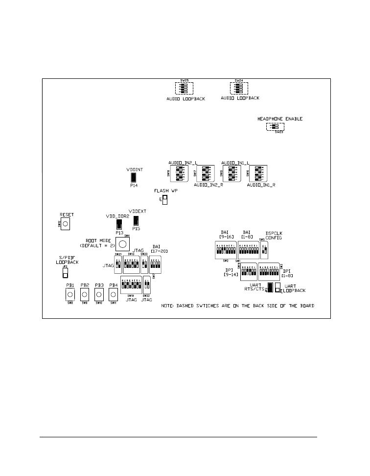
shows the default jumper and switch settings,
connector locations, and LEDs used in installation. Confirm that your
board is in the default configuration before using the board.
The EZ-Board evaluation system contains ESD (electrostatic discharge) sen-
sitive devices. Electrostatic charges readily accumulate on the human body
and equipment and can discharge without detection. Permanent damage may
occur on devices subjected to high-energy discharges. Proper ESD precau-
tions are recommended to avoid performance degradation or loss of function-
ality. Store unused EZ-Board in the protective shipping package.
Default Configuration
1-4
ADSP-21469 EZ-Board Evaluation System Manual
Figure 1-1. Default EZ-Board Hardware Setup

ADSP-21469 EZ-Board Evaluation System Manual
1-5
Using the ADSP-21469 EZ-Board
CCES Install and Session Startup
For information about CCES and to download the software, go to
. A link for the ADSP-21469 EZ-Board Support
Package (BSP) for CCES can be found at
http://www.analog.com/SHARC/EZKits
.
Follow these instructions to ensure correct operation of the product soft-
ware and hardware.
Step 1: Connect the EZ-Board to a personal computer (PC) running
CCES using one of two options: an Analog Devices emulator or via the
debug agent.
Using an Emulator:
1. Plug one side of the USB cable into the USB connector of the emu-
lator. Plug the other side into a USB port of the PC running
CCES.
2. Attach the emulator to the header connector
P1
(labeled
JTAG
) on
the EZ-Board.
Using the standalone Debug Agent:
1. Attach the standalone debug agent to connectors
ZP1
and
ZP4
of
the EZ-Board.
2. Plug one side of the provided USB cable into the USB connector of
the debug agent
ZP1
(labeled
USB
). Plug the other side of the cable
into a USB port of the PC running CCES.

CCES Install and Session Startup
1-6
ADSP-21469 EZ-Board Evaluation System Manual
Step 2: Attach the provided cord and appropriate plug to the 5V power
adaptor.
1. Plug the jack-end of the power adaptor into the power connector
P16
(labeled
5V
) on the EZ-Board.
2. Plug the other side of the power adaptor into a power outlet. The
power LED (labeled
LED9
) is lit green when power is applied to the
board.
3. Power the emulator (if used). Plug the jack-end of the assembled
power adaptor into the emulator and plug the other side of the
power adaptor into a power outlet. The enable/power indicator is
lit green when power is applied.
Step 3 (if connected through the debug agent): Verify that the yellow
USB monitor LED (labeled
LED2
) and the green power LED (labeled
LED1
) on the debug agent are both on. This signifies that the board is com-
municating properly with the host PC and ready to run CCES.
Session Startup
It is assumed that the CrossCore Embedded Studio software is installed
and running on your PC.
Note: If you connect the board or emulator first (before installing
CCES) to the PC, the Windows driver wizard may not find the
board drivers.
1. Navigate to the CCES environment via the Start menu.
Note that CCES is not connected to the target board.

ADSP-21469 EZ-Board Evaluation System Manual
1-7
Using the ADSP-21469 EZ-Board
2. Use the system configuration utility to connect to the EZ-Board.
If a debug configuration exists already, select the appropriate
configuration and click Apply and Debug or Debug. Go to step 8.
To create a debug configuration, do one of the following:
• Click the down arrow next to the little bug icon, select
Debug Configurations
• Choose Run > Debug Configurations.
The Debug Configuration dialog box appears.
3. Select CrossCore Embedded Studio Application and click
(New launch configuration).
The Select Processor page of the Session Wizard appears.
4. Ensure Blackfin is selected in Processor family. In Processor type,
select ADSP-21469. Click Next.
The Select Connection Type page of the Session Wizard appears.
5. Select one of the following:
• For standalone debug agent connections, EZ-Board and
click Next.
• For emulator connections, Emulator and click Next.
The Select Platform page of the Session Wizard appears.

CCES Install and Session Startup
1-8
ADSP-21469 EZ-Board Evaluation System Manual
6. Do one of the following:
• For standalone debug agent connections, ensure that the
selected platform is ADSP-21469 EZ-Board via Debug
Agent.
• For emulator connections, choose the type of emulator that
is connected to the board.
7. Click Finish to close the wizard.
The new debug configuration is created and added to the pro-
gram(s) to load list.
8. In the Program(s) to load section, choose the program to load
when connecting to the board. If not loading any program upon
connection to the target, do not make any changes.
Note that while connected to the target, there is no way to choose a
program to download. To load a program once connected, termi-
nate the session.
To delete a configuration, go to the Debug Configurations dialog
box and select the configuration to delete. Click
and choose Yes
when asked if you wish to delete the selected launch configuration.
Then Close the dialog box.
To disconnect from the target board, click the terminate button
(red box) or choose Run > Terminate.
To delete a session, choose Target > Session > Session List. Select
the session name from the list and click Delete. Click OK.

ADSP-21469 EZ-Board Evaluation System Manual
1-9
Using the ADSP-21469 EZ-Board
VisualDSP++ Install and Session Startup
For information about VisualDSP++ and to download the software, go to
There are two options to connect the EZ-Board hardware to a personal
computer (PC) running VisualDSP++: via an Analog Devices emulator or
via a standalone debug agent module. The standalone debug agent allows
a debug agent to interface to the ADSP-21469 EZ-Board. The standalone
debug agent is shipped with the kit.
To connect the EZ-Board to a PC via an emulator:
1. Plug the 5V adaptor into connector
P16
(labeled
5.0V
).
2. Attach the emulator header to connector
P1
(labeled
JTAG
) on the
back side of the EZ-Board.
To connect the EZ-Board to a PC via a standalone debug agent:
The debug agent can be used only when power is supplied from the
wall adaptor.
1. Attach the standalone debug agent to connectors
P1
(labeled
JTAG
)
and
ZP1
on the backside of the EZ-Board, watching for the keying
pin of
P1
to connect correctly.
2. Plug the 5V adaptor into connector
P16
(labeled
5.0V
).
3. Plug one side of the provided USB cable into a USB connector of
the standalone debug agent. Plug the other side of the cable into
a USB port of the PC running VisualDSP++.
4. Verify that the yellow USB monitor LED on the standalone debug
agent (
LED4
, located on the back side of the board) is lit. This signi-
fies that the board is communicating properly with the host PC
and ready to run VisualDSP++.

VisualDSP++ Install and Session Startup
1-10
ADSP-21469 EZ-Board Evaluation System Manual
Session Startup
1. If you are running VisualDSP++ for the first time, navigate to the
VisualDSP++ environment via the Start > Programs menu. The
main window appears. Note that VisualDSP++ is not connected to
any session. Skip the rest of this step to step 2.
If you have run VisualDSP++ previously, the last opened session
appears on the screen. You can override the default behavior and
force VisualDSP++ to start a new session by pressing and holding
down the Ctrl key while starting VisualDSP++. Do not release the
Ctrl key until the Session Wizard appears on the screen. Go to
step 3.
2. To connect to a new EZ-Board session, start Session Wizard by
selecting one of the following.
• From the Session menu, New Session.
• From the Session menu, Session List. Then click New Ses-
sion from the Session List dialog box.
• From the Session menu, Connect to Target.
3. The Select Processor page of the wizard appears on the screen.
Ensure SHARC is selected in Processor family. In Choose a target
processor, select ADSP-21469. Click Next.
4. The Select Connection Type page of the wizard appears on the
screen. For standalone debug agent connections, select EZ-Board
and click Next. For emulator connections, select Emulator, and
click Next.
5. The Select Platform page of the wizard appears on the screen.
For standalone debug agent connections, ensure that the selected
platform is ADSP-21469 EZ-Board via Debug Agent. For emula-
tor connections, choose the type of emulator that is connected.

ADSP-21469 EZ-Board Evaluation System Manual
1-11
Using the ADSP-21469 EZ-Board
Specify your own Session name for the session or accept the default
name.
The session name can be a string of any length; although, the box
displays approximately 32 characters. The session name can
include space characters. If you do not specify a session name,
VisualDSP++ creates a session name by combining the name of the
selected platform with the selected processor. The only way to
change a session name later is to delete the session and open a new
session.
Click Next.
6. The Finish page of the wizard appears on the screen. The page dis-
plays your selections. Check the selections. If you are not satisfied,
click Back to make changes; otherwise, click Finish. VisualDSP++
creates the new session and connects to the EZ-Board. Once con-
nected, the main window’s title is changed to include the session
name set in step 5.
To disconnect from a session, click the disconnect button
or select Session > Disconnect from Target.
To delete a session, select Session > Session List. Select the session
name from the list and click Delete. Click OK.
CCES Evaluation License
The ADSP-21469 EZ-Board software is part of the Board Support Pack-
age (BSP) for the SHARC ADSP-2146x family. The EZ-Board is a
licensed product that offers an unrestricted evaluation license for 90 days
after activation. Once the evaluation period ends, the evaluation license
becomes permanently disabled. If the evaluation license is installed but

VisualDSP++ Evaluation License
1-12
ADSP-21469 EZ-Board Evaluation System Manual
not activated, it allows 10 days of unrestricted use and then becomes dis-
abled. The license can be re-enabled by activation.
An evaluation license can be upgraded to a full license. Licenses can be
purchased from:
• Analog Devices directly. Call (800) 262-5645 or 781-937-2384 or
go to:
http://www.analog.com/buyonline
.
• Analog Devices, Inc. local sales office or authorized distributor. To
locate one, go to:
http://www.analog.com/salesdir/continent.asp
.
The EZ-Board hardware must be connected and powered up to use
CCES with a valid evaluation or full license.
VisualDSP++ Evaluation License
The ADSP-21469 EZ-Board installation is part of the VisualDSP++
installation. The EZ-Board is a licensed product that offers an unrestricted
evaluation license for the first 90 days. Once the initial unrestricted
90-day evaluation license expires:
• VisualDSP++ restricts a connection to the ADSP-21469 EZ-Board
via the USB port of the standalone debug agent interface only.
Connections to simulators and emulation products are no longer
allowed.
• The linker restricts a user program to 27306 words of memory for
code space with no restrictions for data space.
To avoid errors when opening VisualDSP++, the EZ-KIT Lite
hardware must be connected and powered up. This is true for using
VisualDSP++ with a valid evaluation or full license.
ADSP-21469 EZ-Board Evaluation System Manual
1-13
Using the ADSP-21469 EZ-Board
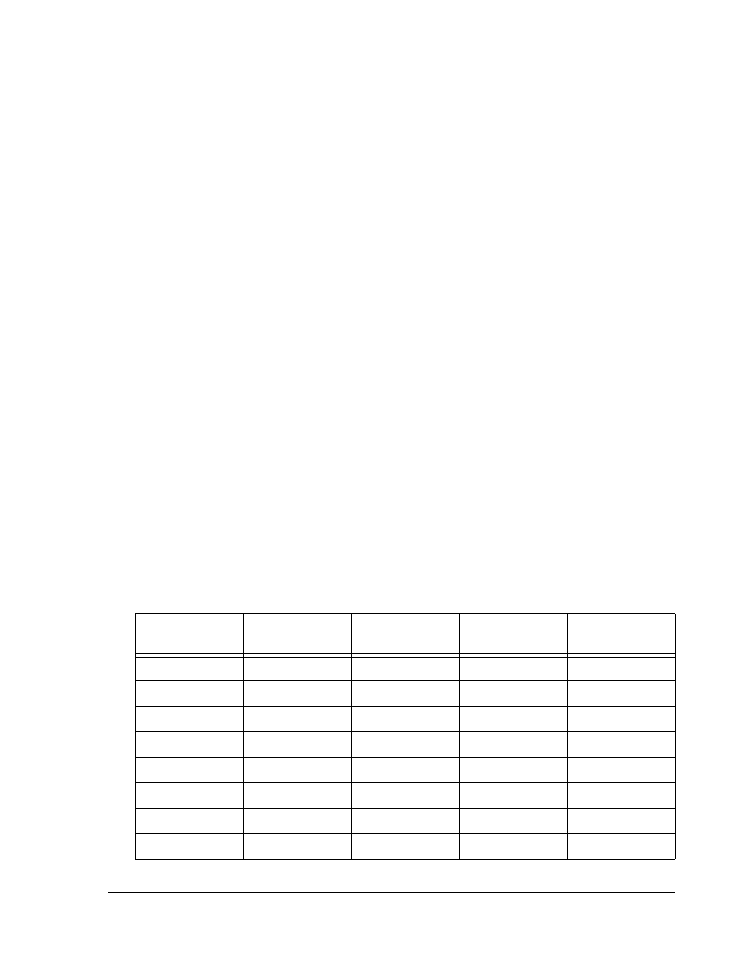
Memory Map
The ADSP-21469 processor has internal static random access memory
(SRAM) for instructions and data storage; see
memory details can be found in the ADSP-214xx SHARC Processor Hard-
ware Reference.
The ADSP-21469 EZ-Board includes three types of external memory:
double data rate two synchronous dynamic random access memory
(DDR2 SDRAM), serial peripheral interconnect (SPI) flash, and parallel
flash. See
. For more information about a specific memory type,
go to the respective section in this chapter.
Table 1-1. Processor Internal Memory Space
Start Address
End Address
Contents
0x0000 0000
0x0003 FFFF
IOP Registers
0x0009 2000
0x0009 DFFF
BLOCK 0 RAM
0x0009 E000
0x000B 1FFF
Reserved
0x000B 2000
0x000B DFFF
BLOCK 1 RAM
0x000B E000
0x000B FFFF
Reserved
0x000C 0000
0x000C 7FFF
BLOCK 2 RAM
0x000C 8000
0x000D FFFF
Reserved
0x000E 0000
0x000E 7FFF
BLOCK 3 RAM
DDR2 Interface
1-14
ADSP-21469 EZ-Board Evaluation System Manual
DDR2 Interface
The ADSP-21469 processor connects to a 128 MB Micron
MT47H64M16HR-3 chip through the DDR2 SDRAM controller. The
DDR2 memory controller on the processor and DDR2 memory chip are
powered by an on-board 1.8V regulator. Data is transferred between the
processor and DDR2 on both the rising and falling edges of the DDR2
clock. The DDR2 controller on the processor can operate at a maximum
clock frequency of half the processor’s core clock. This equates to a DDR2
clock rate of 225 MHz, which is the ADSP-21469 processor limitation.
With a CCES or VisualDSP++ session running and connected to the
EZ-Board via the USB standalone debug agent, the DDR2 registers are
configured automatically each time the processor is reset. The values are
used whenever DDR2 is accessed through the debugger (for example,
when viewing memory windows or loading a program).
To disable the automatic setting of the SDRAM registers, do one of the
following:
• CCES users, choose Target > Settings > Target Options and clear
the Use XML reset values check box.
• VisualDSP++ users, choose Settings > Target Options and clear
the Use XML reset values check box.
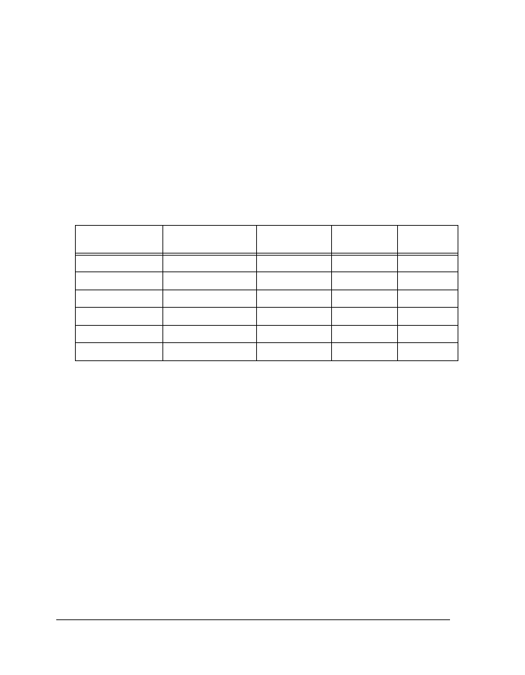
Table 1-2. EZ-Board External Memory Map
Start Address
End Address
Content
0x0020 0000
0x021F FFFF
DDR2 (
DDR2CS0
)
0x0400 0000
0x043F FFFF
Flash memory (
MS1
)
0x0800 0000
0x0800 0000
0x08FF FFFF
0x0BFF FFFF
Unused chip select (
MS2
) for non-DDR2 addresses
Unused chip select (
DDR2_CS2
) for DDR2 addresses
0x0C00 0000
0x0C00 0000
0x0CFF FFFF
0x0FFF FFFF
Unused chip select (
MS3
) for non-DDR2 addresses
Unused chip select (
DDR2_CS3
) for DDR2 addresses

ADSP-21469 EZ-Board Evaluation System Manual
1-15
Using the ADSP-21469 EZ-Board
For more information on changing the reset values, refer to the online
help.
An example program is included in the EZ-Board installation directory to
demonstrate how to setup and access the DDR2 interface.
For more information on how to initialize the registers after a reset, search
the online help for “reset values”.
Parallel Flash Memory Interface
The parallel flash memory interface of the ADSP-21469 EZ-Board con-
tains a 4 MB (4M x 8 bits) Numonyx M29W320EB chip. Flash memory
connects to the 8-bit data bus and address lines 0 through 21. Chip enable
is decoded by the
MS1
select line (default) through switch
SW13
position 2;
see
“Asynchronous Control Enable Switch (SW13)” on page 2-13
the
MS0
line instead of
MS1
to interface to flash memory, make the respec-
tive change to
SW13
. The address range for flash memory is
0x0400 0000
to
0x043F FFFF
.
Flash memory is pre-loaded with boot code for the power-on-self test
(POST) program. For more information, refer to
By default, the EZ-Board boots from the 8-bit parallel flash memory. The
processor boots from flash memory if the boot mode select switch (
SW4
) is
set to position 2; see
“Boot Mode Select Switch (SW4)” on page 2-10
.
Flash memory also is preloaded with configuration flash information, such
as board revision, BOM revision, and other data.
Flash memory code can be modified. For instructions, refer to the online
help and example program included in the EZ-Board installation
directory.
For more information about the parallel flash device, refer to the
Numonyx Web site:
.

SPI Interface
1-16
ADSP-21469 EZ-Board Evaluation System Manual
SPI Interface
The ADSP-21469 processor has two SPI ports which can be accessed via
the digital peripheral interface (DPI) pins.
The SPI flash memory, a 16 Mb ST M25P16 device, connects to the SPI
port of the processor and designates:
• DPI pin 5 (
DPI_P5
) as a chip select
• DPI pin 3 (
DPI_P3
) as the SPI clock
• DPI pin 1 (
DPI_P1
) as the master out slave in (MOSI) pin
• DPI pin 2 (
DPI_P2
) as the master in slave out (MISO) pin
The same SPI port and DPI pins connect to the serial flash memory and
audio codec via switch
SW3
“DPI [1–8] Enable Switch (SW3)” on
. The DPI pins also are available on the expansion interface II.
By default, the EZ-Board boots from the 8-bit flash parallel memory. SPI
flash can be selected as the boot source by setting the boot mode select
switch (
SW4
) to position 1. See
“Boot Mode Select Switch (SW4)” on
.
The audio codec is set up to use DPI pin 4 as the SPI chip select. For more
information, refer to
“Audio Interface” on page 1-19
.
Link Port Interface
The ADSP-21469 processor has two dedicated link ports. Each link port
has a clock pin, an acknowledge pin, and eight data pins. The ports can
operate at up to 166 MHz and act as either a receiver or a transmitter. The
ports can be used to interface gluelessly to other ADSP-21469 processors
that also have the link port pins brought out.

ADSP-21469 EZ-Board Evaluation System Manual
1-17
Using the ADSP-21469 EZ-Board
The EZ-Board enables access to link ports 0 and 1 via connectors
P12
and
J3
, respectively. Two ADSP-21469 EZ-Boards can mate gluelessly via the
link port connectors. The processors can communicate via the link ports,
all while performing independent tasks on each of the EZ-Boards. To
loopback the link port connectors on one EZ-Board or connect three or
more EZ-Boards, obtain a standard, off the shelf connector from Samtec.
For more information, see
“Link Port 0 Connector (P12)” on page 2-30
The EZ-Board design enables a multi-processor JTAG session using con-
nectors
J3
and
P12
. Two or more EZ-Boards can connect via the link ports
and JTAG interfaces and run in a single multi-processor debug session.
For more information, see “JTAG Interface” on page 1-23.
By default, the EZ-Board boots from the 8-bit flash parallel memory. Link
port 0 can be selected as the boot source by setting the boot mode select
switch (
SW4
) to position 4. See
“Boot Mode Select Switch (SW4)” on
.
Temperature Sensor Interface
Two external pins (
THD_P
and
THD_M
) of the processor are connected to an
internal thermal diode. The EZ-Board uses ON Semiconductor’s
ADM1032 digital thermometer and under/over temperature alarm to
monitor the processor’s temperature as well as the thermal diode that
exists inside the ADM1032 device. The device uses the I
2
C bus, DPI pins,
and flag pins to communicate to the processor. The following DPI and
flag pins are used by the processor and temperature sensing monitor.
• DPI pin 8 (
DPI_P8
) as the serial clock signal (
SCK
)
• DPI pin 7 (
DPI_P7
) as the serial data signal (
SDA
)
• Flag 3 as the IRQ (not used by default)
• Flag 0 as the thermal limit (not used by default)

S/PDIF Interface
1-18
ADSP-21469 EZ-Board Evaluation System Manual
The two DPI pins are required; the pins are connected to the temperature
sensing monitor via a switch (
SW3
) and can be shut off if the pins are used
on the expansion II interface. The thermal limit flag is connected to a
LED (
LED11
) for a visual alarm if the limit is exceeded. The thermal limit
flag and ADM1032 IRQ connect to the flag pins of the processor, but are
nonessential for communications. Consequently,
SW13
has both flag pins
defaulted in the
OFF
position.
See
“DPI [1–8] Enable Switch (SW3)” on page 2-9
and
Control Enable Switch (SW13)” on page 2-13
Example programs are included in the EZ-Board installation directory to
demonstrate sensor operations.
S/PDIF Interface
The ADSP-21469 processor has a built-in S/PDIF transmitter and
receiver for digital audio applications. The EZ-Board supports the S/PDIF
interface and brings out both the transmitter and receiver via RCA con-
nectors
J4
and
J5
, respectively. The S/PDIF’s in and out pins are
connected by DAI pins via switches
SW1
and
SW7
:
• DAI pin 1 (
DAI_P1
) as
SPDIF_OUT
• DAI pin 18 (
DPI_P18
) as
SPDIF_IN
SW1
and
SW7
can be turned off to disconnect the DAI pins from the RCA
connectors if the pins are used on the expansion II interface. See

ADSP-21469 EZ-Board Evaluation System Manual
1-19
Using the ADSP-21469 EZ-Board
Audio Interface
The AD1939 device is a high-performance, single-chip codec featuring
eight digital-to-analog converters (DACs) for audio output and four ana-
log-to-digital converters (ADCs) for audio input. This translates to four
stereo channels of audio out and two stereo channels of audio in.
The codec can input and output data at a sample rate of up to 192 kHz on
all channels.
The analog audio channels are available via single-ended RCA connectors
(
J4
and
J5
) or differential DB25 connectors (
P8
and
P9
). By default, the
EZ-Board is shipped with the RCA connectors used by the AD1939 codec
for audio in and out. To use the differential connectors, change DIP
switches
SW15–18
. A standard, off the shelf DB25 connector to XLR cables
is required to operate in this mode.
For more information, see
“Audio In1 Left Selection Switch (SW15)” on
through
“Audio In2 Left Selection Switch (SW18)” on
“ADSP-21469 EZ-Board Schematic” on page B-1
.
The processor interfaces with the codec via the DAI and DPI pins. The
DAI pins can be configured to transfer serial data from the codec in
Time-Division Multiplexing (TDM) or Integrated Interchip Sound (I
2
S)
mode. See
for more information about the
AD1939 connection to the DAI. The DPI interface pins can be config-
ured to use the SPI interface of the processor to set up the codec’s control
registers. See
for more information about the
AD1939 connection to the DPI.
The master input clock (
MCLK
) of the codec is generated by the on-board
12.288 MHz oscillator. The internal PLL of the codec is used to generate
varying sample rates. The codec can be set up for 48 KHz, 96 KHz, or
192 KHz frequencies. The codec can run at these frequencies in both
TDM and I
2
S modes with all ADCs inputs and DACs outputs. To run
192 KHz with all ADCs and DACs in TDM mode, the codec must run in
dual-line TDM mode.

UART Interface
1-20
ADSP-21469 EZ-Board Evaluation System Manual
For information on how to configure the multi-channel codec, refer to the
product datasheet at
.
The EZ-Board is connected to the AD1939 codec in master mode. The
internal PLL drives the
ABCLK
and
ALRCLK
clock signals out. Both clocks
are driven back to the codec’s
DBCLK
and
DLRCLK
pins via the
R257
and
R258
resistors. The
ABCLK
and
ALRCLK
clocks that are driven by the codec also
connect to the processor’s serial ports via the DAI pins. Resistors
R262
and
R263
are used to feed the bit clock and frame sync signals of the processor’s
serial ports. Connecting the codec in this manner enables a flexible audio
sample rate and allows the processor to run at the maximum core
frequency.
The audio interface also has a 3.5 mm connector (
J8
) for headphones. The
headphones share the output with the external
DAC5
and
DAC6
circuits of
the analog audio interface. Switch
SW23
must be enabled for the head-
phones. A volume control potentiometer (
R493
) is used to increase or
decrease the headphone’s volume.
For more information, see “Headphone
Enable Switch (SW23)” on page 2-19.
Example programs are included in the EZ-Board installation directory to
demonstrate how to configure and use the board’s analog audio interface.
The DAI and DPI pins going to the AD1939 device can be disabled, then
used on the expansion II interface. Refer to
for more information about the DAI and
DPI switches.
UART Interface
The ADSP-21469 processor features a built-in universal asynchronous
receiver and transmitter (UART). The UART interface supports full
RS-232 functionality via the Analog Devices 3.3V ADM3202 line driver
and receiver (
U42
). The UART signals are available on the EZ-Board via
DIP switch
SW14
. The UART signals are routed through a DIP switch, can

ADSP-21469 EZ-Board Evaluation System Manual
1-21
Using the ADSP-21469 EZ-Board
be disconnected from the respective DPI interface, and used on the expan-
sion II interface. The following DPI pins are used for the RS-232
interface.
• DPI pin 9 (
DPI_P9
) as
UART_TX
• DPI pin 10 (
DPI_P10
) as
UART_RX
• DPI pin 11 (
DPI_P11
) as
UART_RTS
• DPI pin 12 (
DPI_P12
) as
UART_CTS
Example programs are included in the EZ-Board installation directory to
demonstrate UART and RS-232 operations.
For more information about the UART interface, refer to the
ADSP-214xx SHARC Processor Hardware Reference.
LEDs and Push Buttons
The EZ-Board has eight general-purpose user LEDs connected directly to
the processor, one LED connected to the temperature sensing monitor
(ADM1032), one EZ-Board power LED, and one board reset LED. The
EZ-board also has five push buttons: four general-purpose push buttons,
connected directly to the processor, and one push button for a board reset.
summarizes the LED connections to the processor. To use the
LEDs connected to the DAI or DPI interface, configure the respective reg-
isters of the processor. For more information, refer to the ADSP-214xx
SHARC Processor Hardware Reference.

LEDs and Push Buttons
1-22
ADSP-21469 EZ-Board Evaluation System Manual
Two general-purpose push buttons are attached to the flag pins of the pro-
cessor, while the other two are attached to the DAI pins. All of the push
buttons and LEDs connect to the processor through DIP switches. The
DIP switches can disconnect the processor pins, which, in turn, connect
to the push buttons and LEDs. See the respective switch section in
“ADSP-21469 EZ-Board Hardware Reference” on page 2-1
.
The state of the push buttons, connected to the flag pins, can be deter-
mined by reading the
FLAG
register. The push buttons connected to the
DAI pins must be configured as interrupts. It is necessary to set up an
interrupt routine to determine each pin’s state.
button and processor connections.
Table 1-3. LED Connections
LED Reference Designator
Processor Pin
Connected via Switch
LED1
DPI_P6
SW3.6
LED2
DPI_P13
SW14.5
LED3
DPI_P14
SW14.6
LED4
DAI_P3
SW1.3
LED5
DAI_P4
SW1.4
LED6
DAI_P15
SW2.7
LED7
DAI_P16
SW2.8
LED8
DAI_P17
SW7.1
ADSP-21469 EZ-Board Evaluation System Manual
1-23
Using the ADSP-21469 EZ-Board
An example program is included in the ADSP-21469 installation directory
to demonstrate functionality of the LEDs and push buttons.
JTAG Interface
The JTAG connector (
P1
) allows the standalone debug agent module to
connect a debug session to the ADSP-21469 processor. The debug agent
operates only when the external 5V wall adaptor (
P16
) is used.
The standalone debug agent can be replaced by an external emulator, such
as the Analog Devices high-performance USB-based emulator. Be careful
not to damage the connectors when removing the debug agent. The emu-
lator connects to
P1
on the back side of the board; see
“VisualDSP++ Install and Session
for more information.
The ADSP-21469 EZ-Board can be set up as a single- or multi-processor
system. By default, the board is set up in single-processor mode. In sin-
gle-processor mode, create a session based on a standalone debug agent or
an external emulator. To use the EZ-Board in multi-processor mode,
install an external emulator. Only one external emulator is required for
the main EZ-Board; other EZ-Boards in the JTAG chain do not require
an emulator. In this mode, create a platform based on the number of
JTAG devices in the JTAG chain using the VisualDSP++ Configurator.
Then create a session in VisualDSP++ based on the newly created plat-
form. For multiprocessor mode under CCES, create a platform based on
Table 1-4. Push Button Connections
PB Reference Designator
Processor Pin
Connected via Switch
SW8
(
PB1
)
FLAG1
/
IRQ1
SW13.4
SW9
(
PB2
)
FLAG2
/
IRQ2
/
MS2
SW13.5
SW10
(
PB3
)
DAI_P19
SW7.3
SW11
(
PB4
)
DAI_P20
SW7.4

Land Grid Array
1-24
ADSP-21469 EZ-Board Evaluation System Manual
the number of JTAG devices in the JTAG chain using the Target
Configurator. Then create a Debug Configuration in CCES based on the
newly created platform.
For a dual ADSP-21469 EZ-Board session, connect two EZ-Boards via
connectors
J3
and
P12
. Flip one of the two EZ-Boards by 180 degrees to
allow the boards to mate. To switch between single- and multi-processor
modes, use DIP switches
SW19–22
.
For more information, see “JTAG
Switches (SW19–22)” on page 2-17.
For three or more ADSP-21469 EZ-Board sessions, connect each of the
EZ-Board with the link port cables. The cables connect the link ports and
JTAG pins of each EZ-Board. By using the link port cables, you put the
EZ-Board in a JTAG serial chain and the ADSP-21469 processors’ link
ports in a ring. For three EZ-Boards, three link port cables are required.
Similarly, for four EZ-Boards, four link port cables are required. Note that
each respective EZ-board also requires its own power supply.
Part numbers for Samtec standard, off the shelf link port cables can be
found in
“Link Port 0 Connector (P12)” on page 2-30
For more information about emulators, go to:
http://www.analog.com/processors/tools/sharc
Land Grid Array
The ADSP-21469 EZ-Board has provisions for probing every DAI pin,
DPI pin, and the asynchronous memory interface pins of the processor on
connectors
P5–7
. The connector locations are designed to be used in con-
junction with a Tektronix DMAX logic analyzer connector, but can be
probed with any oscilloscope or logic analyzer. For pinout information,
refer to
“ADSP-21469 EZ-Board Schematic” on page B-1
.
For more information on the Tektronix DMAX logic analyzer interface,
go to the Tektronix Web site.

ADSP-21469 EZ-Board Evaluation System Manual
1-25
Using the ADSP-21469 EZ-Board
Expansion Interface II
The expansion interface II allows an Analog Devices EZ-Extender
®
or a
custom-design daughter board to be tested across various hardware plat-
forms with identical expansion interfaces.
The expansion interface II implemented on the ADSP-21469 EZ-Board
consists of two connectors: a 0.1 in. shrouded header (
P2
) and a Samtec
QMS series header (
J1
). The connectors contain a majority of the
ADSP-21469 processor’s signals.
DDR2 interface is not brought out to the expansion interface
because the interface layout and net length is critical.
For pinout information, go to
“ADSP-21469 EZ-Board Schematic” on
. The mechanical dimensions of the expansion connectors can be
obtained by contacting
.
For more information about daughter boards, visit the Analog Devices
Web site at:
http://www.analog.com/processors/tools/sharc
Limits to current and interface speed must be taken into consideration
when using the expansion interface II. Current for the expansion
interface II is sourced from the EZ-Board; therefore, the current should be
limited to 1A for 5V and 500 mA for the 3.3V planes. If more current is
required, then a separate power connector and a regulator must be
designed on a daughter card. Additional circuitry can add extra loading to
signals, decreasing their maximum effective speed.
Analog Devices does not support and is not responsible for the
effects of additional circuitry.

Power Measurements
1-26
ADSP-21469 EZ-Board Evaluation System Manual
Power Measurements
Several locations are provided for measuring the current draw from vari-
ous power planes. Precision 0.05 ohm shunt resistors are available on the
VDDINT, VDDEXT, and VDD_DDR2 voltage domains. For current
draw measuments, the associated jumper on connector
P13—15
must be
removed. Once the jumper is removed, voltage across the resistor can be
measured using an oscilloscope. Once voltage is measured, current can be
calculated by dividing the voltage by 0.05. For the highest accuracy, a dif-
ferential probe should be used for measuring voltage across the resistor.
For more information, see
“VDD_DDR2 Power Connector (P13)” on
“VDDINT Power Connector (P14)” on page 2-30
, and
“VDDEXT Power Connector (P15)” on page 2-30
.
Power-On-Self Test
The power-on-self-test program (POST) tests all EZ-Board peripherals
and validates functionality as well as connectivity to the processor. Once
assembled, each EZ-Board is fully tested for an extended period of time
with a POST. All EZ-Boards are shipped with the POST preloaded into
one of its on-board flash memories. The POST is executed by resetting the
board and pressing the proper push button(s). The POST also can be used
as a reference in custom software designs or hardware troubleshooting.
Note that the source code for the POST program is included in the instal-
lation directory along with the readme file, which describes how the
EZ-Board is configured to run a POST.
The POST program is only available when using VisualDSP++.

ADSP-21469 EZ-Board Evaluation System Manual
1-27
Using the ADSP-21469 EZ-Board
Example Programs
Example programs are provided with the ADSP-21469 EZ-KIT Lite to
demonstrate various capabilities of the product. The programs are
included in the product installation kit and can be found in the
Examples
folder of the installation. Refer to a readme file provided with each exam-
ple for more information.
CCES users are encouraged to use the example browser to find examples
included with the EZ-KIT Lite Board Support Package.
Board Design Database
A
.zip
file containing all of the electronic information required for the
design, layout, fabrication and assembly of the product is available for
download from the Analog Devices board design database at:

Board Design Database
1-28
ADSP-21469 EZ-Board Evaluation System Manual

ADSP-21469 EZ-Board Evaluation System Manual
2-1
2 ADSP-21469 EZ-BOARD
HARDWARE REFERENCE
This chapter describes the hardware design of the ADSP-21469 EZ-Board
board.
The following topics are covered.
•
“System Architecture” on page 2-2
Describes the ADSP-21469 EZ-Board configuration and explains
how the board components interface with the processor.
•
“Flags and Memory Selects” on page 2-5
Shows the locations and describes the DAI pins, DPI pins, general
purpose flags, and asynchronous memory select lines.
•
“Push Button and Switch Settings” on page 2-7
Shows the locations and describes the push buttons and switches.
•
Shows the locations and describes the configuration jumpers.
•
Shows the locations and describes the LEDs.
•
Shows the locations and provides part numbers for the on-board
connectors. In addition, the manufacturer and part number infor-
mation is provided for the mating parts.
System Architecture
2-2
ADSP-21469 EZ-Board Evaluation System Manual
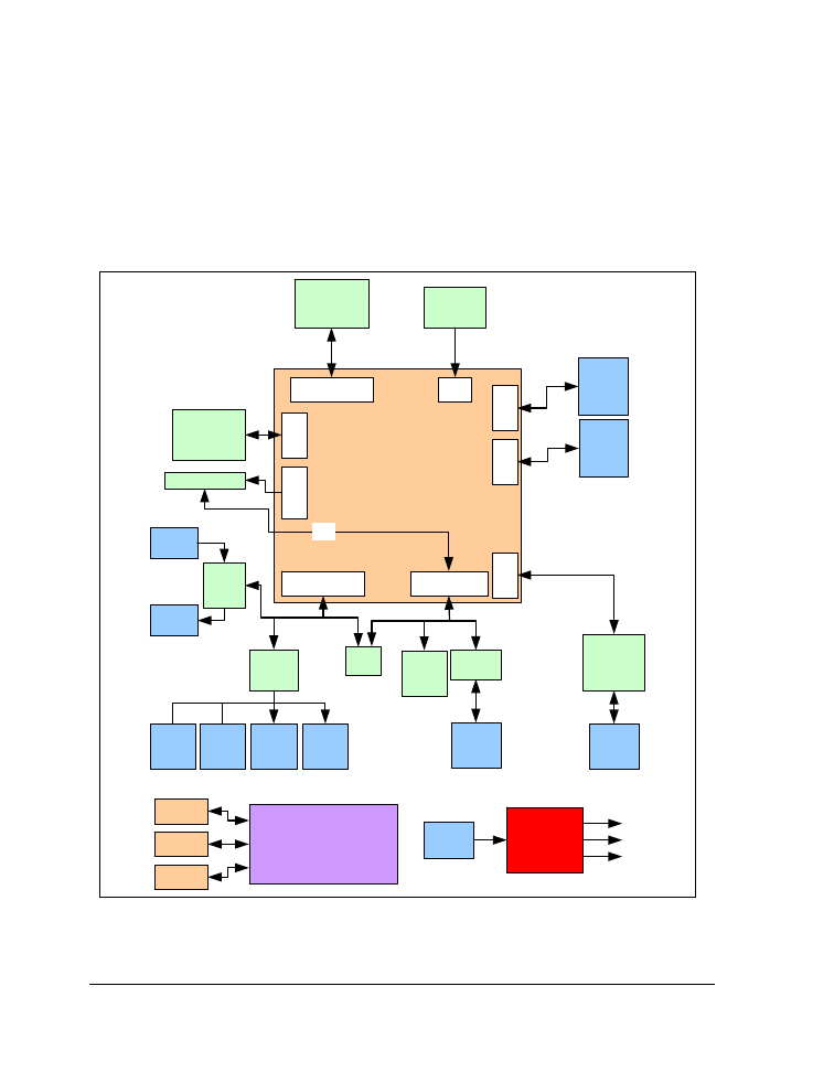
System Architecture
This section describes the processor’s configuration on the EZ-Board
(
Figure 2-1. System Architecture
ADSP-21469
DSP
450 MHz
324-lead PBGA
JT
A
G
Port
128 MB
DDR2
(64M x 16)
25 MHz
Oscillator
DPI
Power
Regulation
AD1939
CODEC
HP
Out
Aud
In
(4)
Head
Out
Aud
Out
(8)
Link
Port 1
AMI
4 MB
Flash
(4M x 8 )
Li
n
k
Po
rt 0
DAI
CLK
TE
MP
Sen
sor
LINK
PORT
CONN
DDR2
JTAG
CONN
Stand
Alone
Debug
Agent
ADM1032
SPI
Flash
16Mb
ADM3202
RS232
CONN
SPDIF
CIRC
SPDIF
IN
SPDIF
OUT
I2C
5V
PWR
IN
3.3V
1.8V
1.1V
Sharc Expansion
Interface II.
DAI = 0.1" Header
DPI = 0.1" Header
AMI = High Speed Conn.
AMI
DAI
DPI
PBs/
LEDs
LINK
PORT
CONN
ADSP-21469 EZ-Board Evaluation System Manual
2-3
ADSP-21469 EZ-Board Hardware Reference
The EZ-Board is designed to demonstrate the ADSP-21469 SHARC pro-
cessor capabilities. The processor has an I/O voltage of 3.3V. The core
voltage of the processor is 1.1V, and the double data rate (DDR2) voltage
is 1.8V.
The input clock is 25 MHz. The default boot mode of the processor is
external parallel flash boot. See
“Boot Mode Select Switch (SW4)” on
for information on how to change the default boot mode.
DAI Interface
The digital application interface (DAI) pins are connected to the signal
routing unit (SRU) of the processor. The SRU is a flexible routing system
providing a large system of signal flows within the processor. The SRU
allows you to route the DAI pins to different internal peripherals in vari-
ous combinations.
The DAI connects various peripherals on the EZ-Board.
shows
the DAI pin names, associated peripheral and net names, switch designa-
tors through which the pins connect to the peripherals, and default switch
settings.
Table 2-1. DAI Connections
DAI Pin
Peripheral
Peripheral Net
Connected via
Switch
Switch Setting
(Default)
DAI_P1
S/PDIF
SPDIF_OUT
SW1.1
ON
DAI_P2
AD1939
SOFT_RESET
SW1.2
ON
DAI_P3
LEDs
LED4
SW1.3
ON
DAI_P4
LEDs
LED5
SW1.4
ON
DAI_P5
AD1939
ASDATA1
SW1.5
ON
DAI_P6
AD1939
ASDATA2
SW1.6
ON
DAI_P7
AD1939
ABCLK
SW1.7
ON
DAI_P8
AD1939
ALRCLK
SW1.8
ON

System Architecture
2-4
ADSP-21469 EZ-Board Evaluation System Manual
To use the DAI on the expansion II interface, disable any signal driving a
DAI pin with the associated switch. The pinout of the expansion connec-
tors can be found in
“ADSP-21469 EZ-Board Schematic” on page B-1
.
DPI Interface
The digital peripheral interface (DPI) pins are connected to a second sig-
nal routing unit of the processor (SRU2). The SRU2 unit, similar to the
SRU, is a flexible routing system providing a large system of signal flows
within the processor. The SRU2 allows you to route the DPI pins to dif-
ferent internal peripherals in various combinations.
The DPI connects various peripherals on the EZ-Board.
shows
the DPI pin names, associated peripheral and net names, switch
designators through which the pins connect to the peripherals, and default
switch settings.
DAI_P9
AD1939
DSDATA4
SW2.1
ON
DAI_P10
AD1939
DSDATA3
SW2.2
ON
DAI_P11
AD1939
DSDATA2
SW2.3
ON
DAI_P12
AD1939
DSDATA1
SW2.4
ON
DAI_P13
AD1939
DBCLK
SW2.5
ON
DAI_P14
AD1939
DLRCLK
SW2.6
ON
DAI_P15
LEDs
LED6
SW2.7
ON
DAI_P16
LEDs
LED7
SW2.8
ON
DAI_P17
LEDs
LED8
SW7.1
ON
DAI_P18
S/PDIF
SPDIF_IN
SW7.2
ON
DAI_P19
Push buttons
PB3
SW7.3
ON
DAI_P20
Push buttons
PB4
SW7.4
ON
Table 2-1. DAI Connections (Cont’d)
DAI Pin
Peripheral
Peripheral Net
Connected via
Switch
Switch Setting
(Default)

ADSP-21469 EZ-Board Evaluation System Manual
2-5
ADSP-21469 EZ-Board Hardware Reference
To use the DPI on the expansion II interface, disable any signal driving a
DPI pin with the associated switch. The pinout of the expansion connec-
tors can be found in
“ADSP-21469 EZ-Board Schematic” on page B-1
.
Flags and Memory Selects
The processor has four asynchronous memory selects, four flag pins, three
interrupt request pins, and one timer expired pin. All flag/memory pins
are multi-functional and depend on the ADSP-21469 processor setup.
shows the pin names, corresponding peripheral and net names,
Table 2-2. DPI Connections
DPI Pin
Peripheral
Peripheral Net
Connected via
Switch
Switch Setting
(Default)
DPI_P1
SPI memory
AD1939
SPI_MOSI
SW3.1
ON
DPI_P2
SPI memory
AD1939
SPI_MISO
SW3.2
ON
DPI_P3
SPI memory
AD1939
SPI_CLK
SW3.3
ON
DPI_P4
AD1939
AD1939_CS
SW3.4
ON
DPI_P5
SPI memory
SPI_CS
SW3.5
ON
DPI_P6
LEDs
LED1
SW3.6
ON
DPI_P7
Temp sensor
TEMP_SDA
SW3.7
ON
DPI_P8
Temp sensor
TEMP_SCK
SW3.8
ON
DPI_P9
UART
UART_TX
SW14.1
ON
DPI_P10
UART
UART_RX
SW14.2
ON
DPI_P11
UART
UART_RTS
SW14.3
OFF
DPI_P12
UART
UART_CTS
SW14.4
OFF
DPI_P13
LEDs
LED2
SW14.5
ON
DPI_P14
LEDs
LED3
SW14.6
ON
Flags and Memory Selects
2-6
ADSP-21469 EZ-Board Evaluation System Manual
switch designators through which the pins connect to the peripherals, and
default switch settings.
To use the flags or memory selects on the expansion II interface, disable
any signal driving a flag or memory pin with the associated switch. The
pinout of the expansion connectors can be found in
EZ-Board Schematic” on page B-1
Table 2-3. Flags and Memory Select Connections
Flag/Memory Pin
Peripheral
Peripheral Net
Connected via
Switch
Switch Setting
(Default)
MS0
Parallel flash memory
FLASH_CS
SW13.1
OFF
MS1
Parallel flash memory
FLASH_CS
SW13.2
ON
FLAG0
/
IRQ0
Temp sensor
THERMAL_LIMIT
SW13.3
OFF
FLAG1
/
IRQ1
Push buttons
PB1
SW13.4
ON
FLAG2
/
IRQ2
/
MS2
Push buttons
PB2
SW13.5
ON
FLAG3
/
TIMEXP
/
MS3
Temp sensor
TEMP_IRQ
SW13.6
OFF
ADSP-21469 EZ-Board Evaluation System Manual
2-7
ADSP-21469 EZ-Board Hardware Reference
Push Button and Switch Settings
This section describes operation of the push buttons and switches. The
push button and switch locations are shown in
.
Figure 2-2. Push Button and Switch Locations

Push Button and Switch Settings
2-8
ADSP-21469 EZ-Board Evaluation System Manual
DAI [1–8] Enable Switch (SW1)
The DAI [1–8] enable switch (
SW1
) disconnects the DAI pins one through
eight on the processor from the associated peripherals on the EZ-Board
and allows the DAI signals to be used on the expansion II interface; see
.
DAI [9–16] Enable Switch (SW2)
The DAI [9–16] enable switch (
SW2
) disconnects the DAI pins nine
through 16 on the processor from the associated peripherals on the
EZ-Board and allows the DAI signals to be used on the expansion II inter-
face; see
.
Table 2-4. DAI [1–8] Enable Switch (SW1)
SW1 Position
DAI Pin
Peripheral
Peripheral Net
Switch Setting
(Default)
SW1.1
DAI_P1
S/PDIF
SPDIF_OUT
ON
SW1.2
DAI_P2
AD1939
SOFT_RESET
ON
SW1.3
DAI_P3
LEDs
LED4
ON
SW1.4
DAI_P4
LEDs
LED5
ON
SW1.5
DAI_P5
AD1939
ASDATA1
ON
SW1.6
DAI_P6
AD1939
ASDATA2
ON
SW1.7
DAI_P7
AD1939
ABCLK
ON
SW1.8
DAI_P8
AD1939
ALRCLK
ON
ADSP-21469 EZ-Board Evaluation System Manual
2-9
ADSP-21469 EZ-Board Hardware Reference
DPI [1–8] Enable Switch (SW3)
The DPI [1–8] enable switch (
SW3
) disconnects the DPI pins one through
eight on the processor from the associated peripherals on the EZ-Board
and allows the DPI signals to be used on the expansion II interface; see
.
Table 2-5. DAI [9–16] Enable Switch (SW2)
SW2 Position
DAI Pin
Peripheral
Peripheral Net
Switch Setting
(Default)
SW2.1
DAI_P9
AD1939
DSDATA4
ON
SW2.2
DAI_P10
AD1939
DSDATA3
ON
SW2.3
DAI_P11
AD1939
DSDATA2
ON
SW2.4
DAI_P12
AD1939
DSDATA1
ON
SW2.5
DAI_P13
AD1939
DBCLK
OFF
SW2.6
DAI_P14
AD1939
DLRCLK
OFF
SW2.7
DAI_P15
LEDs
LED6
ON
SW2.8
DAI_P16
LEDs
LED7
ON
Table 2-6. DPI [1–8] Enable Switch (SW3)
SW3 Position
DPI Pin
Peripheral
Peripheral Net
Switch Setting
(Default)
SW3.1
DPI_P1
SPI memory
AD1939
SPI_MOSI
ON
SW3.2
DPI_P2
SPI memory
AD1939
SPI_MISO
ON
SW3.3
DPI_P3
SPI memory
AD1939
SPI_CLK
ON
SW3.4
DPI_P4
AD1939
AD1939_CS
ON
SW3.5
DPI_P5
SPI memory
SPI_CS
ON
SW3.6
DPI_P6
LEDs
LED1
ON
Push Button and Switch Settings
2-10
ADSP-21469 EZ-Board Evaluation System Manual
Boot Mode Select Switch (SW4)
The boot mode select switch (
SW4
) determines the boot mode of the pro-
cessor.
shows the available boot mode settings. By default, the
processor boots from the on-board parallel flash memory.
The selected position of
SW4
is marked by the notch down the entire rotat-
ing portion of the switch, not the small arrow.
SW3.7
DPI_P7
Temp sensor
TEMP_SDA
ON
SW3.8
DPI_P8
Temp sensor
TEMP_SCK
ON
Table 2-7. Boot Mode Select Switch (SW4)
SW4 Position
Processor Boot Mode
0
SPI slave boot
1
Boot from SPI flash memory (SPI master boot)
2
Boot from 8 external parallel flash memory (default)
3
Reserved
4
Link port 0 boot
5
Reserved
6
Reserved
7
Reserved
Table 2-6. DPI [1–8] Enable Switch (SW3) (Cont’d)
SW3 Position
DPI Pin
Peripheral
Peripheral Net
Switch Setting
(Default)
ADSP-21469 EZ-Board Evaluation System Manual
2-11
ADSP-21469 EZ-Board Hardware Reference
DSP Clock Configuration Switch (SW5)
The clock configuration switch (
SW5
) controls the core frequency of the
processor at power up. The core to clock-in ratio is multiplied by the
25 MHz oscillator (
U41
) to produce the power up core frequency.
shows the switch settings.
The core clock frequency can be increased or decreased via software by
writing to the
PMCTL
register. For more information on changing the core
clock frequency and other settings, refer to the ADSP-214xx SHARC Pro-
cessor Hardware Reference.
DAI [17–20] Enable Switch (SW7)
The DAI [17–20] enable switch (
SW7
) disconnects the DAI pins 17
through 20 on the processor from the associated peripherals on the
EZ-Board and allows the DAI signals to be used on the expansion II inter-
face; see
.
Table 2-8. Processor Clock Configuration Switch (SW5)
Position 1
CLKCFG0
Position 2
CLKCFG0
Clock Ratio
Core: Clock
ON
ON
Reserved
ON
OFF
32:1
OFF
ON
16:1 (default)
OFF
OFF
6:1
Table 2-9. DAI [17–20] Enable Switch (SW7)
SW7 Position
DAI Pin
Peripheral
Peripheral Net
Switch Setting
(Default)
SW7.1
DAI_P17
LEDs
LED8
ON
SW7.2
DAI_P18
S/PDIF
SPDIF_IN
ON

Push Button and Switch Settings
2-12
ADSP-21469 EZ-Board Evaluation System Manual
Programmable Flag Push Buttons (SW8–11)
Four momentary push buttons (
SW8–11
) are provided for general-purpose
user input. The buttons are connected to the GPIO pins of the processor.
The push buttons are active high and, when pressed, send a high (
1
) to the
processor. Switches
SW7
and
SW13
disconnect the push buttons from the
responding signals. Refer to
“DAI [17–20] Enable Switch (SW7)” on
and
“Asynchronous Control Enable Switch (SW13)” on
for more information.
Reset Push Button (SW12)
The reset push button (
SW12
) resets the following ICs:
• ADSP-21469 processor (
U1
)
• AD1939 audio codec (
U45
)
• Parallel flash memory (
U18
)
The reset also is linked to the expansion II interface; any daughter card
connected to the expansion interface that requires a reset can use
SW12
.
The reset push button does not reset the standalone debug agent once the
debug agent is connected to a personal computer (PC). After communica-
tion between the debug agent and PC is initialized, pushing a reset button
does not reset the USB chip on the debug agent. The only way to reset the
USB chip on the debug agent is to power down the EZ-Board.
SW7.3
DAI_P19
Push buttons
PB3
ON
SW7.4
DAI_P20
Push buttons
PB4
ON
Table 2-9. DAI [17–20] Enable Switch (SW7) (Cont’d)
SW7 Position
DAI Pin
Peripheral
Peripheral Net
Switch Setting
(Default)
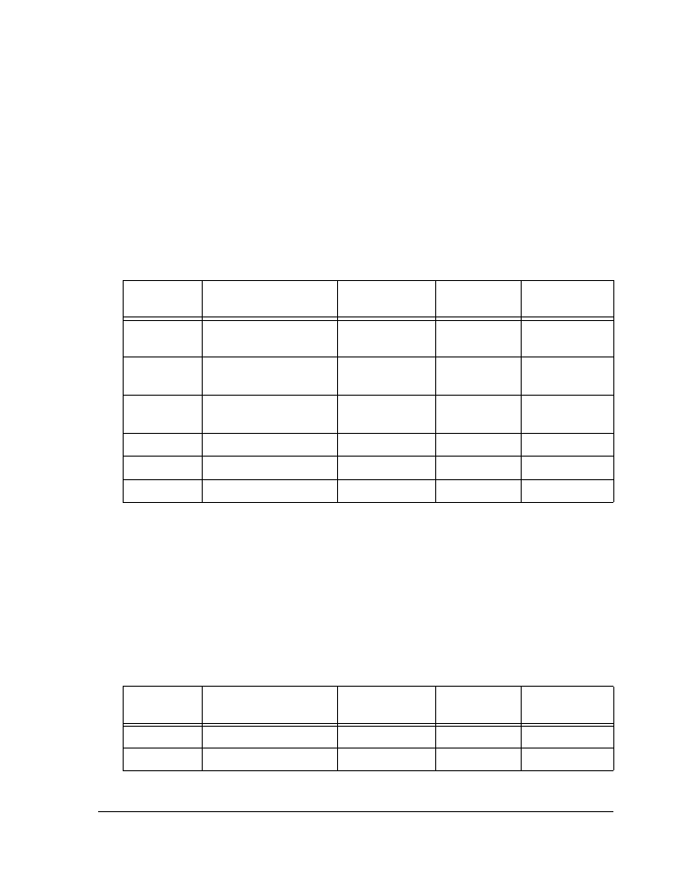
ADSP-21469 EZ-Board Evaluation System Manual
2-13
ADSP-21469 EZ-Board Hardware Reference
Asynchronous Control Enable Switch (SW13)
The asynchronous control enable switch (
SW13
) disconnects the control
pins of the processor from the associated peripherals on the EZ-Board and
allows the respective control signals to be used on the expansion II inter-
face; see
.
DPI [9–14] Enable Switch (SW14)
The DPI [9–14] enable switch (
SW14
) disconnects the DPI pins nine
through 14 on the processors from the associated peripherals on the
EZ-Board and allows the DPI signals to be used on the expansion II inter-
face; see
.
Table 2-10. Asynchronous Control Enable Switch (SW13)
SW13
Position
Processor Pin
Peripheral
Peripheral Net Switch Setting
(Default)
SW13.1
MS0
Parallel flash
memory
FLASH_CS
OFF
SW13.2
MS1
Parallel flash
memory
FLASH_CS
ON
SW13.3
FLAG0
/
IRQ0
Temp sensor
THERMAL
LIMIT
OFF
SW13.4
FLAG1
/
IRQ1
Push buttons
PB1
ON
SW13.5
FLAG2
/
IRQ2
/
MS2
Push buttons
PB2
ON
SW13.6
FLAG3
/
TIMEXP
/
MS3
Temp sensor
TEMP_IRQ
OFF
Table 2-11. DPI [9–14] Enable Switch (SW14)
SW14
Position
DPI Pin
Peripheral
Peripheral Net Switch Setting
(Default)
SW14.1
DPI_P9
UART
UART_TX
ON
SW14.2
DPI_P10
UART
UART_RX
ON
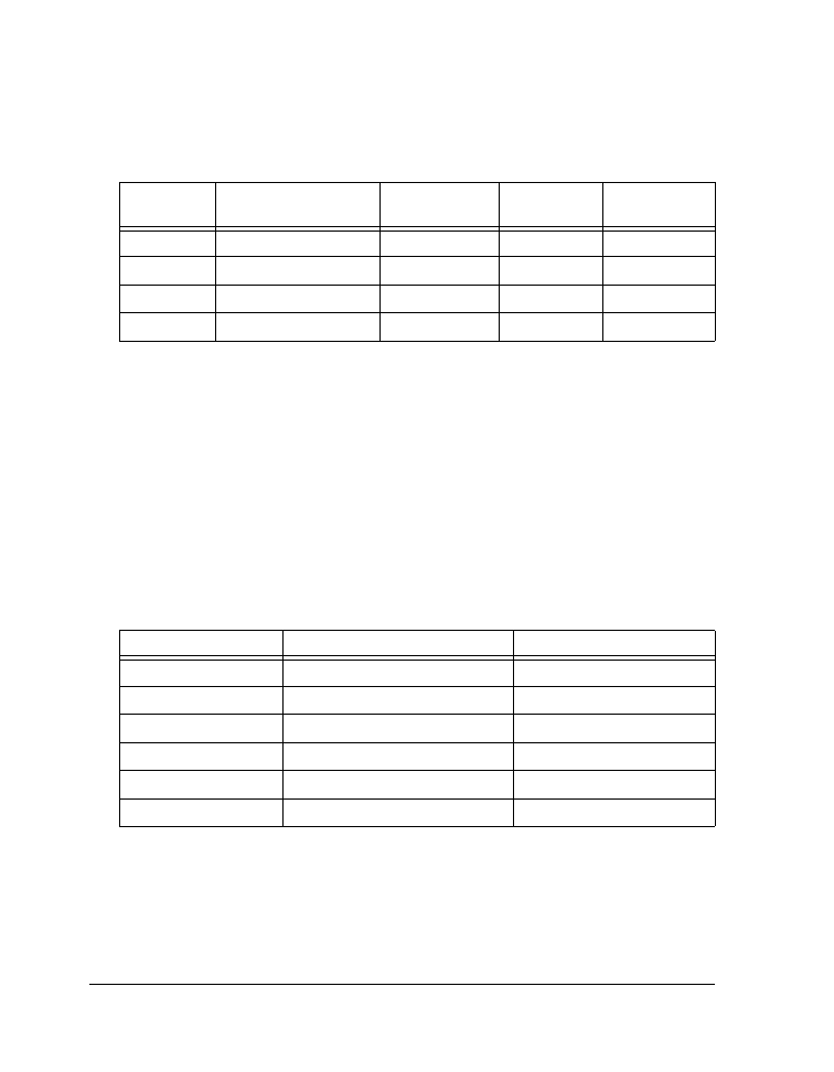
Push Button and Switch Settings
2-14
ADSP-21469 EZ-Board Evaluation System Manual
Audio In1 Left Selection Switch (SW15)
The audio selection switch (
SW15
) connects the left channel of the
In1
line,
connected to the AD1939’s
ADC1
circuit, to either the single-ended RCA
connectors or the differential DB25 connector. By default,
SW15
is set up
to use the RCA connectors. To use the standard, off the shelf DB25 con-
nector to XLR cables, change the switch to the differential setting; see
For more information, see “Differential In/Out Connectors
SW14.3
DPI_P11
UART
UART_RTS
OFF
SW14.4
DPI_P12
UART
UART_CTS
OFF
SW14.5
DPI_P13
LEDs
LED2
ON
SW14.6
DPI_P14
LEDs
LED3
ON
Table 2-12. Audio In1 Left Selection Switch (SW15)
SW15 Position
Single-Ended RCA IN (Default)
Differential DB25 IN (P8)
SW15.1
ON
OFF
SW15.2
OFF
ON
SW15.3
ON
OFF
SW15.4
OFF
ON
SW15.5
ON
OFF
SW15.6
OFF
ON
Table 2-11. DPI [9–14] Enable Switch (SW14) (Cont’d)
SW14
Position
DPI Pin
Peripheral
Peripheral Net Switch Setting
(Default)
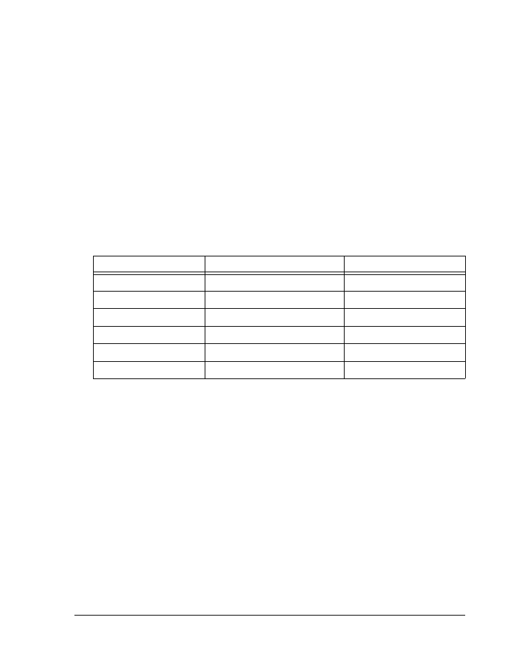
ADSP-21469 EZ-Board Evaluation System Manual
2-15
ADSP-21469 EZ-Board Hardware Reference
Audio In1 Right Selection Switch (SW16)
The audio selection switch (
SW16
) connects the right channel of the
In1
line, connected to the AD1939’s
ADC2
circuit, to either the single-ended
RCA connectors or the differential DB25 connector. By default, the
switch is set up to use the RCA connectors for audio in. To use the stan-
dard, off the shelf DB25 connector to XLR cables, change the switch to
the differential setting; see
For more information, see “Differ-
ential In/Out Connectors (P8–9)” on page 2-29.
Audio In2 Right Selection Switch (SW17)
The audio selection switch (
SW17
) connects the right channel of the
In2
line, connected to the AD1939’s
ADC4
circuit, to either the single-ended
RCA connectors or the differential DB25 connector. By default, the
switch is set up to use the RCA connectors for audio in. To use the stan-
dard, off the shelf DB25 connector to XLR cables, change the switch to
the differential setting; see
For more information, see “Differ-
ential In/Out Connectors (P8–9)” on page 2-29.
Table 2-13. Audio In1 Right Selection Switch (SW16)
SW16 Position
Single-Ended RCA IN (Default)
Differential DB25 IN (P8)
SW16.1
ON
OFF
SW16.2
OFF
ON
SW16.3
ON
OFF
SW16.4
OFF
ON
SW16.5
ON
OFF
SW16.6
OFF
ON
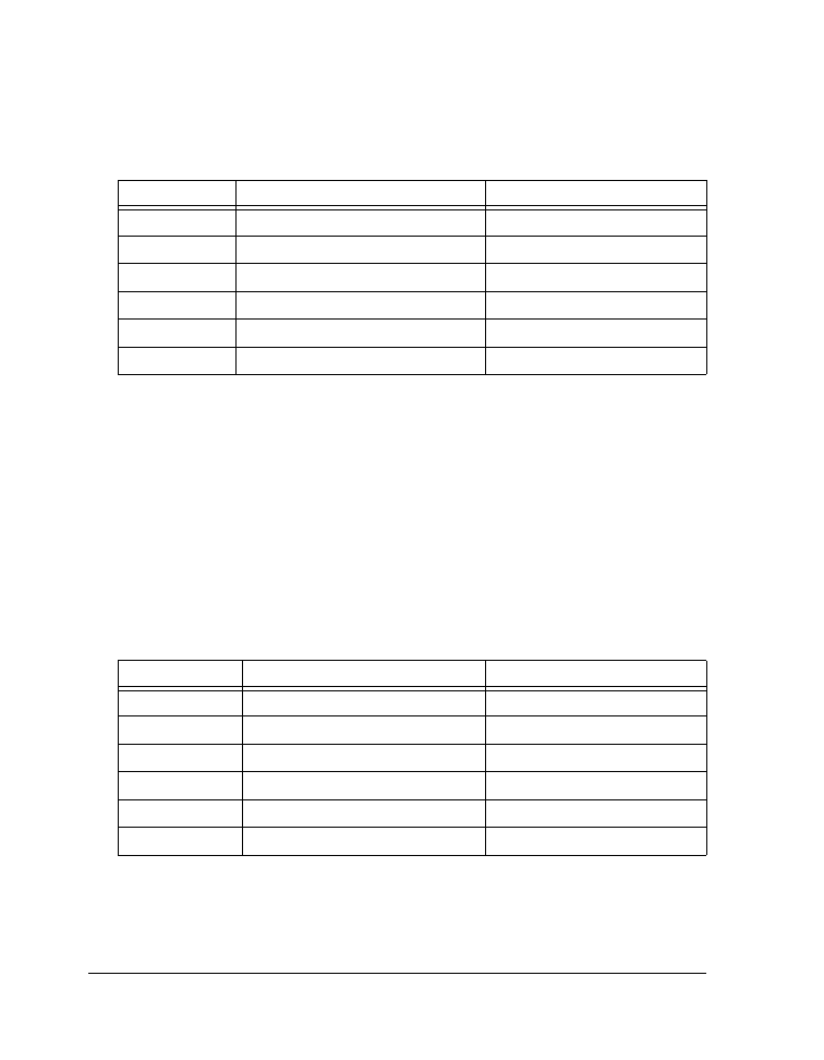
Push Button and Switch Settings
2-16
ADSP-21469 EZ-Board Evaluation System Manual
Audio In2 Left Selection Switch (SW18)
The audio selection switch (
SW18
) connects the left channel of the
In2
line,
connected to the AD1939’s
ADC3
circuit, to either the single-ended RCA
connectors or the differential DB25 connector. By default, the switch is
set up to use the RCA connectors for audio in. To use the standard, off
the shelf DB25 connector to XLR cables, change the switch to the differ-
ential setting; see
.
For more information, see “Differential
In/Out Connectors (P8–9)” on page 2-29.
Table 2-14. Audio In2 Right Selection Switch (SW17)
SW17 Position
Single Ended Use RCA IN (Default)
Differential DB25 IN (P8)
SW17.1
ON
OFF
SW17.2
OFF
ON
SW17.3
ON
OFF
SW17.4
OFF
ON
SW17.5
ON
OFF
SW17.6
OFF
ON
Table 2-15. Audio In2 Left Selection Switch (SW18)
SW18 Position
Single Ended RCA IN (Default)
Differential DB25 IN (P8)
SW18.1
ON
OFF
SW18.2
OFF
ON
SW18.3
ON
OFF
SW18.4
OFF
ON
SW18.5
ON
OFF
SW18.6
OFF
ON

ADSP-21469 EZ-Board Evaluation System Manual
2-17
ADSP-21469 EZ-Board Hardware Reference
JTAG Switches (SW19–22)
The JTAG switches (
SW19–22
) select between a single-processor (one
EZ-Board) and multi-processor (more than one EZ-Board) configura-
tions. By default, the four DIP switches are set up for a single EZ-Board
configuration; see
The default configuration applies to either a debug agent or an external
emulator, such as the Analog Devices high-performance USB-based emu-
lator (HP-USB ICE for short). To use an external emulator and multiple
EZ-Boards simultaneously in one multi-processor session, set up the
boards as shown in
. Attach the boards to each other via con-
nectors
J3
and
P12
. For two EZ-Boards, no external cables are required.
For three or more EZ-Boards, obtain Samtec link port cables described in
“Link Port 1 Connector (J3)” on page 2-26
and
.
Table 2-16. Single-Processor Configuration
Switch Position
Single EZ-Board Use (Default)
SW19.1
ON
SW19.2
OFF
SW19.3
ON
SW19.4
OFF
SW19.5
ON
SW19.6
OFF
SW19.7
ON
SW19.8
OFF
SW20.1
ON
SW20.2
OFF
SW21.1
ON
SW21.2
OFF
Push Button and Switch Settings
2-18
ADSP-21469 EZ-Board Evaluation System Manual
SW22.1
OFF
SW22.2
OFF
Table 2-17. Multiple-Processor Configuration
Switch Position
Main EZ-Board
Attached to Emulator
EZ-Board(s)
Not Attached to Emulator
SW19.1
ON
OFF
SW19.2
ON
ON
SW19.3
ON
OFF
SW19.4
ON
ON
SW19.5
ON
OFF
SW19.6
ON
ON
SW19.7
ON
OFF
SW19.8
ON
ON
SW20.1
ON
OFF
SW20.2
OFF
OFF
SW21.1
OFF
OFF
SW21.2
ON
ON
SW22.1
OFF
ON
SW22.2
ON
OFF
Table 2-16. Single-Processor Configuration (Cont’d)
Switch Position
Single EZ-Board Use (Default)

ADSP-21469 EZ-Board Evaluation System Manual
2-19
ADSP-21469 EZ-Board Hardware Reference
Headphone Enable Switch (SW23)
The headphone enable switch (
SW23
) connects the AD1939’s
OUT3
circuit
to the 3.5 mm headphone connector (
J8
). By default, the headphone
enable switch is disabled. To use the headphones, set
SW23
to all
ON
.
more information, see “Headphone Out Connector (J8)” on page 2-28.
Audio Loopback Switches (SW24–25)
The audio loopback switches (
SW24
and
SW25
) are used for testing only.
The switches loop back any analog signal generated from the AD1939’s
digital-to-analog converter (DAC) circuit to analog-to-digital converter
(ADC) circuit.
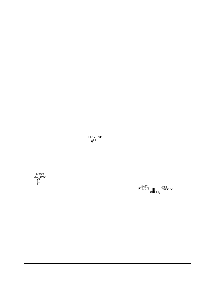
Jumpers
2-20
ADSP-21469 EZ-Board Evaluation System Manual
Jumpers
This section describes functionality of the configuration jumpers.
Figure 2-3. Configuration Jumper Locations

ADSP-21469 EZ-Board Evaluation System Manual
2-21
ADSP-21469 EZ-Board Hardware Reference
Flash WP Jumper (JP1)
The flash WP jumper (
JP1
) write-protects block 0 of the parallel flash
chip. Block 0 is located at address range
0x0400 0000–0x0400 1FFF
. The
POST begins at block 0 and continues on to other blocks in flash mem-
ory. When the jumper is installed on
JP1
, and the parallel flash driver
from Analog Devices is used, block 0 is read-only. By default,
JP1
is not
installed.
S/PDIF Loopback Jumper (JP2)
The S/PDIF loop back jumper (
JP2
) is used for internal testing only. The
jumper loops back any digital audio signal from the S/PDIF’s
Data Out
pin to the S/PDIF’s
Data In
pin. By default,
JP2
is not installed.
UART RTS/CTS Jumper (JP3)
The UART RTS/CTS jumper (
JP3
) connects the
RTS
and
CTS
pins of the
RS-232 interface. By default,
JP3
is installed.
UART Loopback Jumper (JP4)
The UART loop back jumper (
JP4
) is used for internal testing only. The
jumper loops back the UART receive data from the UART transmit data.
By default,
JP4
is not installed.
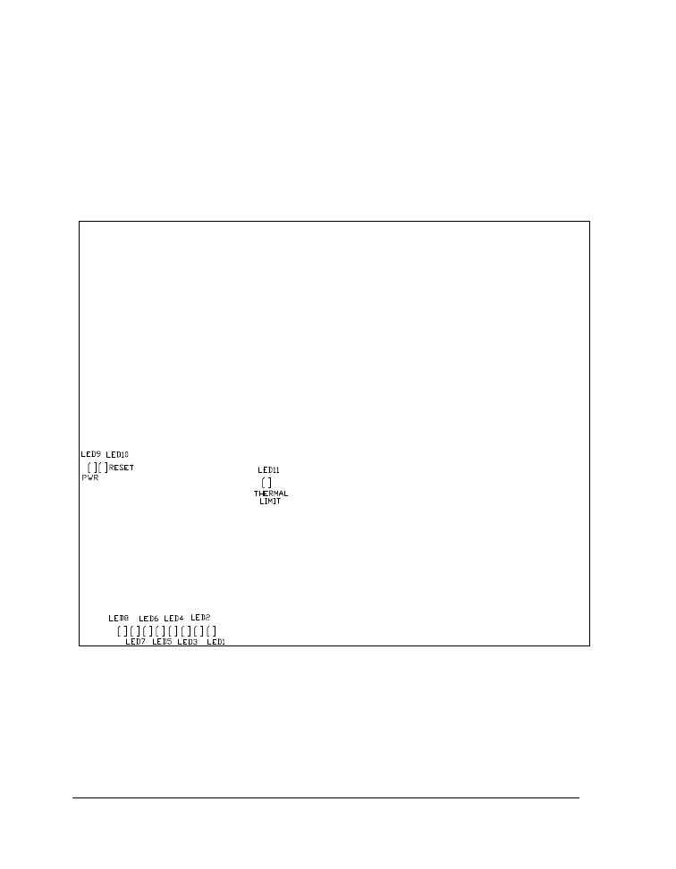
LEDs
2-22
ADSP-21469 EZ-Board Evaluation System Manual
LEDs
This section describes the on-board LEDs.
shows the LED
locations.
Figure 2-4. LED Locations
ADSP-21469 EZ-Board Evaluation System Manual
2-23
ADSP-21469 EZ-Board Hardware Reference
GPIO LEDs (LED1–8)
Eight LEDs connect to the DAI and DPI pins of the processor; see
. The LEDs are active high and lit by writing a ‘
1
’ to the correct
DAI or DPI pin.
Power LED (LED9)
When
LED9
is lit solid, it indicates that the board is powered.
Reset LED (LED10)
When
LED10
is lit, it indicates that a master reset of all major ICs is active.
The reset LED is controlled by the Analog Devices ADM708 supervisory
reset circuit. You can assert the reset push button (
SW12
) to assert a master
reset and activate
LED10
.
For more information, see “Reset Push Button
Table 2-18. GPIO LEDs
LED Reference Designator
Processor Pin
LED1
DPI_P6
LED2
DPI_P13
LED3
DPI_14
LED4
DAI_P3
LED5
DAI_P4
LED6
DAI_P15
LED7
DAI_P16
LED8
DAI_P17

LEDs
2-24
ADSP-21469 EZ-Board Evaluation System Manual
Thermal Limit LED (LED11)
The thermal limit LED (
LED11
) reports a status of the thermal sensor,
ADM1032 (
U43
). The thermal sensor monitors the processor’s tempera-
ture. When the high temperature limit set by the IC is violated,
LED11
is
turned on as a visual indicator. The ADM1032 has built-in hysteresis,
which causes the LED to de-activate only when the temperature is signifi-
cantly within the limit.
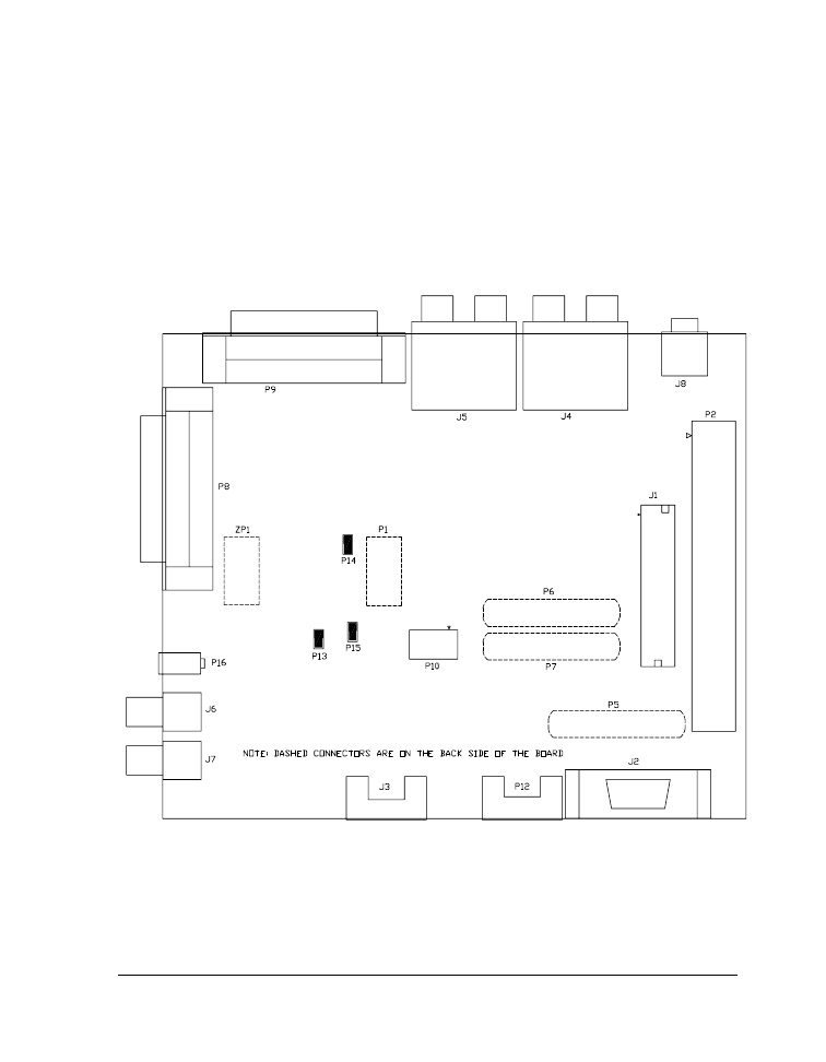
ADSP-21469 EZ-Board Evaluation System Manual
2-25
ADSP-21469 EZ-Board Hardware Reference
Connectors
This section describes connector functionality and provides information
about mating connectors. The connector locations are shown in
Figure 2-5. Connector Locations

Connectors
2-26
ADSP-21469 EZ-Board Evaluation System Manual
Expansion Interface II Connector (J1)
J1
is a board-to-board connector providing signals from the asynchronous
memory interface (AMI) of the processor. The connector is located on the
right edge of the board. For more information, see
. For availability and pricing of the connector, contact
Samtec.
RS-232 Connector (J2)
Link Port 1 Connector (J3)
Part Description
Manufacturer
Part Number
104-position 0.025”, SMT header
SAMTEC
QMS-052-06.75-L-D-A
Mating Connector
104-position 0.025”, SMT socket
SAMTEC
QFS-052-04.25-L-D-A
Part Description
Manufacturer
Part Number
DB9, female, vertical mount
NORCOMP
191-009-213-L-571
Mating Cable
2m female-to-female cable
DIGI-KEY
AE1020-ND
Part Description
Manufacturer
Part Number
ERF8 10X2, RA female
SAMTEC
ERF8-010-01-S-D-RA-L
Mating Cable
6” cable ERF8 to ERM8 10X2
SAMTEC
ERCD-010-06.00-TBL-SBR-1
ADSP-21469 EZ-Board Evaluation System Manual
2-27
ADSP-21469 EZ-Board Hardware Reference
RCA Audio Connector (J4)
RCA Audio Connector (J5)
S/PDIF IN Connector (J6)
S/PDIF OUT Connector (J7)
Part Description
Manufacturer
Part Number
RCA 2x3
KYOYAKU ENT
WSP-256V1-09
Mating Cable (shipped with the EZ-KIT)
6' RCA audio cable
CABLESTOGO
03171
Part Description
Manufacturer
Part Number
RCA 2x3
KYOYAKU ENT
WSP-256V1-09
Mating Cable (shipped with the EZ-KIT)
6' RCA audio cable
CABLESTOGO
03171
Part Description
Manufacturer
Part Number
RCA 1X1
SWITCHCRAFT
PJRAN1X1U01X
Mating Cable (shipped with the EZ-KIT)
6' RCA audio cable
CABLESTOGO
03171
Part Description
Manufacturer
Part Number
RCA 1X1
SWITCHCRAFT
PJRAN1X1U01X
Mating Cable (shipped with the EZ-KIT)
6' RCA audio cable
CABLESTOGO
03171
Connectors
2-28
ADSP-21469 EZ-Board Evaluation System Manual
Headphone Out Connector (J8)
JTAG Connector (P1)
The
P1
connector provides access to the JTAG signals of the ADSP-21469
processor. The standalone debug agent requires two connectors,
P1
and
ZP1
. Pin 3 is missing to provide keying. Pin 3 in the mating connector
must have a plug.
For more information, see “JTAG Interface” on
Remove the standalone debug agent when an emulator is used with the
EZ-Board. Follow the installation instructions provided in
and Session Startup” on page 1-5
or
“VisualDSP++ Install and Session
P1
as the JTAG connection point.
Expansion Interface II Connector (P2)
P2
is a board-to-board connector providing signals for the DAI and DPI
interfaces and GPIO signals of the processor. The connector is located on
the right edge of the board.
For more information, see “Expansion Inter-
For availability and pricing of the connectors,
contact Samtec.
Part Description
Manufacturer
Part Number
3.5mm stereo_jack
CUI
SJ1-3525NG
Mating Headphones (shipped with the EZ-KIT)
Stereo headphones
KOSS
151225 UR5
Part Description
Manufacturer
Part Number
60-position 0.1”, SMT header
SAMTEC
TSSH-130-01-L-DV-A
Mating Connector
60-position 0.1”, SMT socket
SAMTEC
SSW-130-22-F-D-VS

ADSP-21469 EZ-Board Evaluation System Manual
2-29
ADSP-21469 EZ-Board Hardware Reference
DMAX Land Grid Array Connectors (P5–7)
The land grid array areas (
P5–7
) are intended for probing of the processor
signals. The pads are exposed and designed to attach a Tektronix logic
analyzer to the connectors listed in the following table. For more informa-
tion about the land grid array, consult the Tektronix Web site.
Differential In/Out Connectors (P8–9)
The differential in and out connectors (
P8–9
) are intended for an evalua-
tion of the AD1939 codec via XLR connectors. A standard, off the shelf
DB25 connector to XLR cables is required; the cable details can be found
in the following table.
MLB Connector (P10)
The media local bus (MLB) connector (
P10
) is intended for an evaluation
of the ADSP-21462 processor’s MLB interface.
P10
is not available on the
ADSP-21469 EZ-Board because the ADSP-21469 processor does not sup-
port MLB.
Part Description
Manufacturer
Part Number
Primary retention
TEKTRONIX
020290800
Alternate retention
TEKTRONIX
020291000
Part Description
Manufacturer
Part Number
25-position DB25 socket
TYCO
1734350-2
Mating cables
Snake (8)XLRF-25P 9.9’
HOSA
DTF-803
Snake (8)XLRM-25P 9.9’
HOSA
DTM-803
Connectors
2-30
ADSP-21469 EZ-Board Evaluation System Manual
Link Port 0 Connector (P12)
VDD_DDR2 Power Connector (P13)
The
VDD_DDR2
power connector (
P13
) is used to measure voltage and cur-
rent supplied to the DDR2 memory interface of the processor. By default,
P13
is
ON
, and the power flows through the two-pin IDC header. To mea-
sure power, remove the jumper on
P13
and measure voltage across the
0.1 ohm resistor. Once voltage is measured, power can be calculated. For
more information, refer to
“Power Measurements” on page 1-26
.
VDDINT Power Connector (P14)
The
VDDINT
power connector (
P14
) is used to measure voltage and current
supplied to the processor core. By default,
P14
is
ON
, and the power flows
through the two-pin IDC header. To measure power, remove the jumper
on
P14
and measure voltage across the 0.1 ohm resistor. Once voltage is
measured, power can be calculated. For more information, refer to
VDDEXT Power Connector (P15)
The
VDDEXT
power connector (
P15
) is used to measure the processor’s I/O
voltage and current. By default,
P15
is
ON
, and the power flows through the
two-pin IDC header. To measure power, remove the jumper on
P15
and
measure voltage across the 0.1 ohm resistor. Once voltage is measured,
power can be calculated. For more information, refer to
.
Part Description
Manufacturer
Part Number
ERM8 10X2, RA Male
SAMTEC
ERM8-010-01-S-D-RA
Mating Cable
6” cable ERF8 to ERM8 10X2
SAMTEC
ERCD-010-06.00-TBL-SBR-1
ADSP-21469 EZ-Board Evaluation System Manual
2-31
ADSP-21469 EZ-Board Hardware Reference
Power Connector (P16)
The power connector (
P16
) provides all of the power necessary to operate
the EZ-Board.
Standalone Debug Agent Connector (ZP1)
ZP1
connects the standalone debug agent to the EZ-Board. The standalone
debug agent requires two connectors,
ZP1
and
P1
.
see “JTAG Connector (P1)” on page 2-28.
Part Description
Manufacturer
Part Number
0.65 mm power jack
CUI
045-0883R
Mating Power Supply (shipped with the EZ-Board and EZ-KIT)
5.0VDC@3.6A power supply
GLOBTEK
GS-1750(R)

Connectors
2-32
ADSP-21469 EZ-Board Evaluation System Manual

ADSP-21469 EZ-Board Evaluation System Manual
A-1
A ADSP-21469 EZ-BOARD BILL
OF MATERIALS
The bill of materials corresponds to
“ADSP-21469 EZ-Board Schematic”
.
Ref.
Qty.
Description
Reference Designator
Manufacturer
Part Number
1
1
74LVC14A
SOIC14
U14
TI
74LVC14AD
2
1
IDT74FCT3244
APY SSOP20
U17
IDT
IDT74FCT3244APYG
3
1
12.288MHZ
OSC003
U12
EPSON
SG-8002CA MP
4
1
25MHZ OSC003
U41
EPSON
SG-8002CA MP
5
3
SN74LVC1G08
SOT23-5
U48-50
TI
SN74LVC1G08DBVR
6
1
SN65LVDS2D
SOIC8
U44
NATIONAL
SEMI
DS90LV018ATM
7
1
M25P16 SO8W
U40
ST MICRO
M25P16-VMW6G
8
1
MT47H64M16
FBGA84
U2
MICRON
MT47H64M16HR-3
9
1
ADM1032
SOIC_N8
U43
ON SEMI
ADM1032ARZ
10
2
SI7601DN
ICS010
U15-16
VISHAY
SI7601DN
11
1
21469
M29W320EB
"U18"
U18
ST MICRO
M29W320EB70ZE6E

A-2
ADSP-21469 EZ-Board Evaluation System Manual
12
1
ADM708SARZ
SOIC8
U46
ANALOG
DEVICES
ADM708SARZ
13
1
ADM3202ARNZ
SOIC16
U42
ANALOG
DEVICES
ADM3202ARNZ
14
1
ADSP-21469
PBGA324
U1
ANALOG
DEVICES
ADSP-21469KBZ-ENG
15
2
ADP1864AUJZ
SOT23-6
VR2-3
ANALOG
DEVICES
ADP1864AUJZ-R7
16
1
ADP1710
TSOT5
VR1
ANALOG
DEVICES
ADP1710AUJZ-R7
17
1
ADP1715
MSOP8
VR4
ANALOG
DEVICES
ADP1715ARMZ-1.8-R7
18
1
AD1939 LQFP64
U45
ANALOG
DEVICES
AD1939YSTZ
19
16
AD8652ARZ
SOIC_N8
U20-26,U28-30,U32-3
4,U36-38
ANALOG
DEVICES
AD8652ARZ
20
1
AD8397
SOIC_N8_EP
U51
ANALOG
DEVICES
AD8397ARDZ
21
1
ADM1085
SC70_6
U52
ANALOG
DEVICES
ADM1085AKSZ-REEL7
22
2
RCA 1X1
CON012
J6-7
SWITCH-
CRAFT
PJRAN1X1U01X
23
5
MOMENTARY
SWT013
SW8-12
PANASONIC
EVQ-PAD04M
24
4
DIP8 SWT016
SW1-3,SW19
C&K
TDA08H0SB1
25
6
DIP6 SWT017
SW13-18
CTS
218-6LPST
26
3
DIP4 SWT018
SW7,SW24-25
ITT
TDA04HOSB1
27
1
DB9 9PIN
CON038
J2
NORCOMP
191-009-213-L-571
28
5
DIP2 SWT020
SW5,SW20-23
C&K
CKN9064-ND
Ref.
Qty.
Description
Reference Designator
Manufacturer
Part Number

ADSP-21469 EZ-Board Evaluation System Manual
A-3
ADSP-21469 EZ-Board Bill Of Materials
29
3
IDC 2X1
IDC2X1
P13-15
FCI
90726-402HLF
30
4
IDC 2X1
IDC2X1
JP1-4
FCI
90726-402HLF
31
3
IDC
2PIN_JUMPER_
SHORT
SJ1-3
DIGI-KEY
S9001-ND
32
1
3.5MM
STEREO_JACK
CON001
J8
DIGI-KEY
CP1-3525NG-ND
33
1
PWR .65MM
CON045
P16
CUI
045-0883R
34
1
5A RESETABLE
FUS005
F1
MOUSER
650-RGEF500
35
1
QMS 52x2
QMS52x2_SMT
J1
SAMTEC
QMS-052-06.75-L-D-A
36
1
IDC 7x2
IDC7x2_SMTA
P1
SAMTEC
TSM-107-01-T-DV-A
37
1
ROTARY
SWT027
SW4
COPAL
S-8110
38
2
RCA 2x3
CON_RCA_6B
J4-5
KYOYAKU
ENT.
WSP-256V1-09
39
1
ERM8 10X2
ERM8_10X2_S
MT
P12
SAMTEC
ERM8-010-01-S-D-RA
40
1
ERF8 10X2
ERF8_10X2_SM
T
J3
SAMTEC
ERF8-010-01-S-D-RA-L
41
2
DB25 25PIN
DB25F
P8-9
TYCO
1734350-2
42
1
IDC 30x2
IDC30X2_SMTA
P2
SAMTEC
TSSH-130-01-L-DV-A
Ref.
Qty.
Description
Reference Designator
Manufacturer
Part Number

A-4
ADSP-21469 EZ-Board Evaluation System Manual
43
9
YELLOW
LED001
LED1-8,LED11
PANASONIC
LN1461C
44
2
22PF 50V 5%
0805
C262-263
AVX
08055A220JAT
45
2
0.22UF 25V 10%
0805
C126-127
AVX
08053C224KAT2A
46
1
0.1UF 50V 10%
0805
C123
AVX
08055C104KAT
47
1
600 100MHZ
200MA 0603
FER5
DIGI-KEY
490-1014-2-ND
48
2
600 100MHZ
500MA 1206
FER7-8
STEWARD
HZ1206B601R-10
49
2
10UF 16V 20%
CAP002
CT59-60
PANASONIC
EEE1CA100SR
50
1
190 100MHZ 5A
FER002
FER9
MURATA
DLW5BSN191SQ2
51
8
10UF 6.3V 10%
0805
C97-98,C100-101,
C103-104,C254,
C257
AVX
08056D106KAT2A
52
2
4.7UF 6.3V 10%
0805
C240,C246
AVX
08056D475KAT2A
53
35
0.1UF 10V 10%
0402
C26-27,C53,C117-
120,C148,C151-152,
C160,C162,C169-
170,C178,C188-189,
C191,C197,C199-
200,C211,C213-214,
C225,C227-228,
C237,C264,C267-
271,C273
AVX
0402ZD104KAT2A
Ref.
Qty.
Description
Reference Designator
Manufacturer
Part Number

ADSP-21469 EZ-Board Evaluation System Manual
A-5
ADSP-21469 EZ-Board Bill Of Materials
54
94
0.01UF 16V 10%
0402
C28,C30-43,C45-50,
C52,C54-96,C99,
C102,C105-116,
C121-122,C125,
C128-131,C136-142,
C266
AVX
0402YC103KAT2A
55
33
10K 1/16W 5%
0402
R99,R190,R196-200,
R202,R205-210,R217,
R224-225,R233-239,
R256,R259-260,
R463-466,R469,R494
VISHAY
CRCW040210K0FKED
56
2
4.7K 1/16W 5%
0402
R185,R501
VISHAY
CRCW04024K70JNED
57
4
0 1/16W 5%
0402
R462,R485,R492,
R498
PANASONIC
ERJ-2GE0R00X
58
1
22 1/16W 5%
0402
R230
PANASONIC
ERJ-2GEJ220X
59
13
33 1/16W 5%
0402
R191-192,R201,
R203-204,R211,
R257-258,R261-263,
R495-496
VISHAY
CRCW040233R0JNEA
60
1
100UF 10V 10%
C
CT61
AVX
TPSC107K010R0075
61
2
2.2UF 10V 10%
0805
C238-239
AVX
0805ZD225KAT2A
62
1
1000PF 50V 5%
0402
C51
AVX
04025C102JAT2A
63
2
1A SK12
DO-214AA
D4-5
DIODES INC
B120B-13-F
64
1
107.0 1/10W 1%
0805
R228
DIGI-KEY
311-107CRTR-ND
65
1
249.0 1/10W 1%
0805
R227
DIGI-KEY
311-249CRTR-ND
Ref.
Qty.
Description
Reference Designator
Manufacturer
Part Number

A-6
ADSP-21469 EZ-Board Evaluation System Manual
66
2
0.1UF 16V 10%
0603
C255-256
AVX
0603YC104KAT2A
67
2
1UF 16V 10%
0603
C260-261
PANASONIC
ECJ-1VB1C105K
68
2
68PF 50V 5%
0603
C243,C249
AVX
06035A680JAT2A
69
2
470PF 50V 5%
0603
C242,C248
AVX
06033A471JAT2A
70
1
220UF 6.3V 20%
D2E
CT45
SANYO
10TPE220ML
71
11
330 1/10W 5%
0603
R248-255,R467-468,
R497
VISHAY
CRCW0603330RJNEA
72
2
0 1/10W 5%
0603
R452,R458
PHYCOMP
232270296001L
73
4
10 1/10W 5%
0603
R244-247
VISHAY
CRCW060310R0JNEA
74
1
10.0K 1/16W 1%
0603
R231
DALE
CRCW060310K0FKEA
75
8
237.0 1/10W 1%
0603
R267,R272,R280,
R285,R293,R298-299,
R304
DIGI-KEY
311-237HRTR-ND
76
24
49.9K 1/10W 1%
0603
R265,R271,R282,
R284,R295,R297,
R300,R302,R310,
R336-337,R343-344,
R363-364,R369,R378,
R397-398,R403,R412,
R431-432,R437
DIGI-KEY
311-49.9KHRTR-ND
77
1
75.0 1/10W 1%
0603
R229
DALE
CRCW060375R0FKEA
78
4
1UF 6.3V 20%
0402
C132-135
PANASONIC
ECJ-0EB0J105M
Ref.
Qty.
Description
Reference Designator
Manufacturer
Part Number

ADSP-21469 EZ-Board Evaluation System Manual
A-7
ADSP-21469 EZ-Board Bill Of Materials
79
4
100 1/16W 5%
0402
R240-243
DIGI-KEY
311-100JRTR-ND
80
1
562.0 1/10W 1%
0603
R461
VISHAY
CRCW0603562RFKEA
81
1
390PF 25V 5%
0603
C258
AVX
06033A391FAT2A
82
1
5600PF 16V 5%
0805
C259
AVX
0805YA562JAT2A
83
1
15.0K 1/16W 1%
0603
R232
DIGI-KEY
311-15.0KHRTR-ND
84
40
4.99K 1/16W 1%
0603
R264,R273,R278-279,
R291-292,R305-306,
R311,R313-314,R324,
R326-328,R342,
R349-350,R352-354,
R357,R366,R371,
R383-384,R386-388,
R391,R400,R405,
R417-418,R420-422,
R425,R434,R439
VISHAY
CRCW06034K99FKEA
85
2
24.9K 1/10W 1%
0603
R448,R454
DIGI-KEY
311-24.9KHTR-ND
86
1
31.6K 1/16W 1%
0603
R473
PANASONIC
ERJ-3EKF3162V
87
3
10UF 10V 10%
0805
C29,C161,C265
PANASONIC
ECJ-2FB1A106K
88
8
5.76K 1/16W 1%
0603
R266,R269,R277,
R281,R290,R294,
R303,R307
PANASONIC
ERJ-3EKF5761V
89
3
0.05 1/2W 1%
1206
R446,R459-460
SEI
CSF 1/2 0.05 1%R
90
3
10UF 16V 10%
1210
C244-245,C250
AVX
1210YD106KAT2A
91
1
GREEN LED001
LED9
PANASONIC
LN1361CTR
Ref.
Qty.
Description
Reference Designator
Manufacturer
Part Number

A-8
ADSP-21469 EZ-Board Evaluation System Manual
92
1
RED LED001
LED10
PANASONIC
LN1261CTR
93
2
1000PF 50V 5%
1206
C236,C251
AVX
12065A102JAT2A
94
1
255.0K 1/10W
1% 0603
R447
VISHAY
CRCW06032553FK
95
2
80.6K 1/10W 1%
0603
R449,R455
DIGI-KEY
311-80.6KHRCT-ND
96
3
5A
MBRS540T3G
SMC
D1-3
ON SEMI
MBRS540T3G
97
2
2.5UH 30%
IND013
L1-2
COILCRAFT
MSS1038-252NLB
98
3
1.0K 1/16W 1%
0402
R194-195,R287
PANASONIC
ERJ-2RKF1001X
99
1
8.20K 1/10W 1%
0603
R502
DIGI-KEY
541-8.20KHCT-ND
100
6
10.0K 1/16W 1%
0402
R474,R486-488,R491,
R499
DIGI-KEY
541-10.0KLCT-ND
101
10
100K 1/16W 5%
0402
R475-484
DIGI-KEY
541-100KJTR-ND
102
1
30.9K 1/16W 1%
0402
R453
DIGI-KEY
541-30.9KLCT-ND
103
25
33 1/32W 5%
RNS005
RN1-14,RN18,RN22,
RN26-34
PANASONIC
EXB-28V330JX
104
4
51.1 1/16W 1%
0402
R218-221
DIGI-KEY
541-51.1LCT-ND
105
16
2.67K 1/16W 1%
0402
R316,R318,R322,
R338,R367-368,R373,
R377,R401-402,R407,
R411,R435-436,R441,
R445
PANASONIC
ERJ-2RKF2671X
Ref.
Qty.
Description
Reference Designator
Manufacturer
Part Number

ADSP-21469 EZ-Board Evaluation System Manual
A-9
ADSP-21469 EZ-Board Bill Of Materials
106
31
100.0 1/16W 1%
0402
R193,R274-275,R288,
R309,R331-335,R340,
R351,R358-362,R385,
R392-396,R419,
R426-430,R489-490
DIGI-KEY
541-100LCT-ND
107
2
47UF 16V 20%
ELEC_6MM
CT57-58
PANASONIC
EEE-FC1C470P
108
4
37.4K 1/16W 1%
0402
R268,R276,R289,
R308
DIGI-KEY
541-37.4KLCT-ND
109
8
1000PF 50V 5%
0402
C144,C150,C154,
C159,C164,C168,
C171,C176
DIGI-KEY
490-3244-1-ND
110
4
100pF 50V 5%
0402
C147,C155,C165,
C175
MURATA
GCM1555C1H101JZ13
D
111
8
300PF 100V 5%
0603
C143,C145,C153,
C157,C163,C173,
C177,C179
DIGI-KEY
490-1362-1-ND
112
16
2.43K 1/16W 1%
0402
R315,R319,R323,
R325,R346-347,
R374-375,R380-381,
R408-409,R414-415,
R442-443
DIGI-KEY
541-2.43KLCT-ND
113
16
750.0 1/16W 1%
0402
R317,R320-321,R341,
R345,R348,R372,
R376,R379,R382,
R406,R410,R413,
R416,R440,R444
DIGI-KEY
541-750LCT-ND
114
16
620PF 50V 5%
0402
C181,C186-187,
C192,C194-195,
C201,C204,C208-
209,C215,C218,
C222-223,C229,C232
DIGI-KEY
490-3239-1-ND
Ref.
Qty.
Description
Reference Designator
Manufacturer
Part Number

A-10
ADSP-21469 EZ-Board Evaluation System Manual
115
16
680PF 50V 5%
0402
C182-183,C185,
C193,C202-203,
C206-207,C216-217,
C220-221,C230-231,
C234-235
DIGI-KEY
490-3240-1-ND
116
4
0.036 1/2W 1%
1206
R450-451,R456-457
SUSUMU
RL1632S-R036-F
117
1
470UF 2.5V 20%
D2E
CT47
SANYO
2R5TPE470MF
118
40
22UF 6.3V 20%
ELEC_4MM
CT1,CT3,CT5-6,
CT8-11,CT14,CT16,
CT18-19,CT23-24,
CT27-28,CT31-32,
CT35-36,CT39-40,
CT43-44,CT49-56,
CT62-69
PANASONIC
EEE-FC0J220R
119
8
22UF 6.3V 20%
ELEC_5MM
C180,C184,C196,
C205,C210,C219,
C224,C233
MOUSER
647-UWP0J220MCL
120
1
5K 1/20W 20%
RES_POT_DUA
L
R493
PANASONIC
EVJ-Y15F03A53
121
4
51 1/32W 5%
RNS005
RN35-38
DIGI-KEY
EXB-28V510JX
122
9
10 1/32W 5%
RNS005
RN15-17,RN19-21,
RN23-25
PANASONIC
EXB-28V100JX
123
9
82 1/32W 5%
RNS005
RN40-48
PANASONIC
EXB-28V820JX
124
9
47PF 50V 10%
CNS001
CN1-9
TDK CORP
CKCL44C0G1H470K
125
16
6.81K 1/10W 1%
0603
R312,R329-330,R339,
R355-356,R365,R370,
R389-390,R399,R404,
R423-424,R433,R438
DIGI-KEY
311-6.81KHRTR-ND
Ref.
Qty.
Description
Reference Designator
Manufacturer
Part Number

ADSP-21469 EZ-Board Evaluation System Manual
A-11
ADSP-21469 EZ-Board Bill Of Materials
126
1
806 1/10W 1%
0402
R286
VISHAY
CRCW0402806RFKED
127
1
30A GSOT05
SOT23-3
D6
VISHAY
GSOT05-GS08
128
2
30A GSOT03
SOT23-3
D7,D10
VISHAY
GSOT03-GS08
129
1
40A
ESD5Z2.5T1
SOD-523
D8
ON SEMI
ESD5Z2.5T1G
130
1
7A
VESD01-02V-GS
08 SOD-52
D9
VISHAY
VESD01-02V-GS08
131
1
16.9K 1/16W 1%
0402
R500
VISHAY
CRCW040216K9FKED
Ref.
Qty.
Description
Reference Designator
Manufacturer
Part Number

A-12
ADSP-21469 EZ-Board Evaluation System Manual
3-13-2009_14:36
D
4
3
2
1
A
B
C
20 Cotton Road
Nashua, NH 03063
A
B
C
D
4
3
2
1
PH: 1-800-ANALOGD
C
Title
Size
Board No.
Date
Sheet
of
DEVICES
ANALOG
Rev
A0221-2008
ADSP-21469 EZ-BOARD
0.2
SCHEMATIC
ADSP-21469 EZ-BOARD
1
16
TITLE
R4B
R3B
R2B
R1B
R1A
R2A
R4A
R3A
R4B
R3B
R2B
R1B
R1A
R2A
R4A
R3A
R4B
R3B
R2B
R1B
R1A
R2A
R4A
R3A
R4B
R3B
R2B
R1B
R1A
R2A
R4A
R3A
R4B
R3B
R2B
R1B
R1A
R2A
R4A
R3A
R4B
R3B
R2B
R1B
R1A
R2A
R4A
R3A
R4B
R3B
R2B
R1B
R1A
R2A
R4A
R3A
R4B
R3B
R2B
R1B
R1A
R2A
R4A
R3A
R4B
R3B
R2B
R1B
R1A
R2A
R4A
R3A
R4B
R3B
R2B
R1B
R1A
R2A
R4A
R3A
R4B
R3B
R2B
R1B
R1A
R2A
R4A
R3A
R4B
R3B
R2B
R1B
R1A
R2A
R4A
R3A
R4B
R3B
R2B
R1B
R1A
R2A
R4A
R3A
D
4
3
2
1
A
B
C
20 Cotton Road
Nashua, NH 03063
A
B
C
D
4
3
2
1
PH: 1-800-ANALOGD
C
Title
Size
Board No.
Date
Sheet
of
DEVICES
ANALOG
Rev
A0221-2008
ADSP-21469 EZ-BOARD
0.2
R4B
R3B
R2B
R1B
R1A
R2A
R4A
R3A
DDR2_ADDR0
DDR2_ADDR1
DDR2_ADDR10
DDR2_ADDR11
DDR2_ADDR12
DDR2_ADDR13
DDR2_ADDR14
DDR2_ADDR15
DDR2_ADDR2
DDR2_ADDR3
DDR2_ADDR4
DDR2_ADDR5
DDR2_ADDR6
DDR2_ADDR7
DDR2_ADDR8
DDR2_ADDR9
DDR2_BA0
DDR2_BA1
DDR2_BA2
DDR2_CKE
DDR2_CLK0
DDR2_CLK1
DDR2_DATA0
DDR2_DATA1
DDR2_DATA10
DDR2_DATA11
DDR2_DATA12
DDR2_DATA13
DDR2_DATA14
DDR2_DATA15
DDR2_DATA2
DDR2_DATA3
DDR2_DATA4
DDR2_DATA5
DDR2_DATA6
DDR2_DATA7
DDR2_DATA8
DDR2_DATA9
DDR2_DM0
DDR2_DM1
DDR2_DQS0
DDR2_DQS1
DDR2_ODT
VREF1
VREF2
DDR2_CAS
DDR2_CLK0
DDR2_CLK1
DDR2_CS0
DDR2_CS1
DDR2_CS2
DDR2_CS3
DDR2_DQS0
DDR2_DQS1
DDR2_RAS
DDR2_WE
A0
A1
A10/AP
A11
A12
A2
A3
A4
A5
A6
A7
A8
A9
BA0
BA1
BA2
CK
CKE
DQ0
DQ1
DQ10
DQ11
DQ12
DQ13
DQ14
DQ15
DQ2
DQ3
DQ4
DQ5
DQ6
DQ7
DQ8
DQ9
GND1
GND2
GND3
GND4
GND5
GNDL
GNDQ1
GNDQ10
GNDQ2
GNDQ3
GNDQ4
GNDQ5
GNDQ6
GNDQ7
GNDQ8
GNDQ9
LDM
LDQS
NC1
NC2
ODT
RFU/A13
RFU/A14
RFU/A15
UDM
UDQS
VDD1
VDD2
VDD3
VDD4
VDD5
VDDL
VDDQ1
VDDQ10
VDDQ2
VDDQ3
VDDQ4
VDDQ5
VDDQ6
VDDQ7
VDDQ8
VDDQ9
VREF
CAS
CK
CS
LDQS
RAS
UDQS
WE
For a custom design, please adhere to any EE-note from ADI
and any recommendations by the memory manufacturer.
DDR2 end of line terminators and VTT tracking circuit have been
omitted since overall trace length is less than 2.5" for each net.
P9
N1
J3
E3
A3
E7
F2
F8
H2
H8
K9
J1
E9
G1
G3
R7
A8
E8
K8
C9
C7
C3
C1
A9
D8
D2
B8
B2
A7
C2
C8
F9
F1
H9
H1
B9
B1
D9
D1
D3
D7
G2
G8
E2
A2
L2
P3
P8
P2
N7
N3
N8
N2
M7
P7
M2
M3
F7
B7
R8
R3
L3
L1
G9
G7
B3
F3
K7
L7
K3
L8
K2
A1
E1
J9
M9
R1
J7
J2
R2
H7
J8
M8
H3
U2
FBGA84
MT47H64M16
D11
C18
C17
B1
C7
C10
C9
D2
C2
D1
B13
A13
B7
A7
C11
C3
A10
B10
B4
A12
B11
A11
A9
B9
A8
B8
C16
B16
A16
D16
A15
B15
C15
D15
D13
C13
D14
C14
B14
A14
A2
B3
A3
B5
A5
B6
A6
B2
B12
A4
A17
B17
C1
B18
E1
D4
ADSP-21469
PBGA324
U1
5
6
7
8
1
2
4
3
RN3
RNS005
33
2
16
3-31-2009_10:10
DSP - DDR2 INTERFACE
3
4
2
1
8
7
6
5
RN2
RNS005
33
3
4
2
1
8
7
6
5
RN11
RNS005
33
5
6
7
8
1
2
4
3
RN12
RNS005
33
3
4
2
1
8
7
6
5
RN13
RNS005
33
5
6
7
8
1
2
4
3
RN14
RNS005
33
5
6
7
8
1
2
4
3
RN10
RNS005
33
3
4
2
1
8
7
6
5
RN9
RNS005
33
5
6
7
8
1
2
4
3
RN8
RNS005
33
3
4
2
1
8
7
6
5
RN7
RNS005
33
5
6
7
8
1
2
4
3
RN1
RNS005
33
3
4
2
1
8
7
6
5
RN6
RNS005
33
5
6
7
8
1
2
4
3
RN5
RNS005
33
3
4
2
1
8
7
6
5
RN4
RNS005
33
R193
100.0
0402
R195
1.0K
0402
0402
0.01UF
C30
C29
10UF
0805
C28
0.01UF
0402
C27
0.1UF
0402
C26
0.1UF
0402
R191
0402
33
R192
0402
33
R194
1.0K
0402
C31
0.01UF
0402
0402
0.01UF
C32
C36
0.01UF
0402
0402
0.01UF
C35
C34
0.01UF
0402
0402
0.01UF
C33
C42
0.01UF
0402
0402
0.01UF
C41
C40
0.01UF
0402
0402
0.01UF
C39
C38
0.01UF
0402
0402
0.01UF
C37
C43
0.01UF
0402
3.3V
3.3V
0
1
2
3
4
5
6
7
3.3V
GND
OE
OUT
VDD
3.3V
3.3V
3.3V
3.3V
3.3V
3.3V
3.3V
1
2
ON
D
4
3
2
1
A
B
C
20 Cotton Road
Nashua, NH 03063
A
B
C
D
4
3
2
1
PH: 1-800-ANALOGD
C
Title
Size
Board No.
Date
Sheet
of
DEVICES
ANALOG
Rev
A0221-2008
ADSP-21469 EZ-BOARD
0.2
R4B
R3B
R2B
R1B
R1A
R2A
R4A
R3A
R4B
R3B
R2B
R1B
R1A
R2A
R4A
R3A
R4B
R3B
R2B
R1B
R1A
R2A
R4A
R3A
R4B
R3B
R2B
R1B
R1A
R2A
R4A
R3A
R4B
R3B
R2B
R1B
R1A
R2A
R4A
R3A
R4B
R3B
R2B
R1B
R1A
R2A
R4A
R3A
R4B
R3B
R2B
R1B
R1A
R2A
R4A
R3A
R4B
R3B
R2B
R1B
R1A
R2A
R4A
R3A
R4B
R3B
R2B
R1B
R1A
R2A
R4A
R3A
R4B
R3B
R2B
R1B
R1A
R2A
R4A
R3A
R4B
R3B
R2B
R1B
R1A
R2A
R4A
R3A
R4B
R3B
R2B
R1B
R1A
R2A
R4A
R3A
R4B
R3B
R2B
R1B
R1A
R2A
R4A
R3A
R4B
R3B
R2B
R1B
R1A
R2A
R4A
R3A
R4B
R3B
R2B
R1B
R1A
R2A
R4A
R3A
R4B
R3B
R2B
R1B
R1A
R2A
R4A
R3A
R4B
R3B
R2B
R1B
R1A
R2A
R4A
R3A
C1A
C1B
C2A
C2B
C3A
C3B
C4A
C4B
C1A
C1B
C2A
C2B
C3A
C3B
C4A
C4B
C1A
C1B
C2A
C2B
C3A
C3B
C4A
C4B
C1A
C1B
C2A
C2B
C3A
C3B
C4A
C4B
C1A
C1B
C2A
C2B
C3A
C3B
C4A
C4B
C1A
C1B
C2A
C2B
C3A
C3B
C4A
C4B
C1A
C1B
C2A
C2B
C3A
C3B
C4A
C4B
C1A
C1B
C2A
C2B
C3A
C3B
C4A
C4B
C1A
C1B
C2A
C2B
C3A
C3B
C4A
C4B
R4B
R3B
R2B
R1B
R1A
R2A
R4A
R3A
R4B
R3B
R2B
R1B
R1A
R2A
R4A
R3A
R4B
R3B
R2B
R1B
R1A
R2A
R4A
R3A
AMI_ACK
AMI_ADDR0
AMI_ADDR1
AMI_ADDR10
AMI_ADDR11
AMI_ADDR12
AMI_ADDR13
AMI_ADDR14
AMI_ADDR15
AMI_ADDR16
AMI_ADDR17
AMI_ADDR18
AMI_ADDR19
AMI_ADDR2
AMI_ADDR20
AMI_ADDR21
AMI_ADDR22
AMI_ADDR23
AMI_ADDR3
AMI_ADDR4
AMI_ADDR5
AMI_ADDR6
AMI_ADDR7
AMI_ADDR8
AMI_ADDR9
AMI_DATA0
AMI_DATA1
AMI_DATA2
AMI_DATA3
AMI_DATA4
AMI_DATA5
AMI_DATA6
AMI_DATA7
BOOT_CFG0
BOOT_CFG1
BOOT_CFG2
CLKIN
CLKOUT
CLK_CFG0
CLK_CFG1
FLAG0/IRQ0
FLAG1/IRQ1
FLAG2/IRQ2/AMI_MS2
FLAG3/TIMEXP/AMI_MS3
MLBCLK
MLBD0
MLBDAT
MLBSIG
MLBSO
TCK
TDI
TDO
THD_M
THD_P
TMS
XTAL
AMI_MS0
AMI_MS1
AMI_WR
AM_RD
EMU
RESET
TRST
3.3V
3.3V
A0
A1
A10
A11
A12
A13
A14
A15
A16
A17
A18
A19
A2
A20
A3
A4
A5
A6
A7
A8
A9
D0
D1
D10
D11
D12
D13
D14
D15/A-1
D2
D3
D4
D5
D6
D7
D8
D9
GND1
GND2
NC
RY/BY~
VDD
BYTE
CE
OE
RESET
VPP/WP~
WE
MLB_DEVICE
D_MINUS
D_PLUS
GND
SCK
SI
VCC
ALERT
THERM
3.3V
1
2
4
5
6
ON
3
6:1
ON
ON
OFF
OFF
OFF
ON
OFF
DSP OSC
OSC
MLB NOT SUPPORTED ON 21469 DSP
P10 UNPOPULATED BY DEFAULT
SPI Master Boot
16:1
Reserved
Reserved
SPI Slave Boot
CLKCFG0
2
1
CLKCFG1
0
1
2
4
Link Port 0 Boot
CLOCK RATIO
CORE:CLKIN
32:1
SW13: ASYNC CONTROL ENABLE
JP1 DEFAULT: OFF
XTAL PIN TEST POINT
DO NOT POPULATE C44
DEFAULT
DEFAULT: OFF ON OFF ON ON OFF
SW5: DSP CLOCK CONFIG
P10 CAN BE USED WITH A 21462 DSP
ON
AMI Boot (Parallel Flash)
SW4: BOOT MODE SELECT
POSITION
BOOT MODE
DEFAULT
3,5,6 or 7
R196
10K
0402
0.01UF
0402
C46
1
2
3
4
5
6
7
8
9
10
11
12
SW13
DIP6
SWT017
2
3
7
8
4
6
1
5
U43
SOIC_N8
ADM1032
1
10
2
3
4
6
7
8
9
5
P10
5X2_2MM
DNP
R203
0402
33
E1
C5
D5
B6
A6
C6
D6
B2
C3
D4
C1
D3
A1
B1
D2
C2
A2
B5
A5
E2
H2
F3
G3
F4
G5
F5
E3
H3
H4
E4
H5
E5
F2
G2
H6
A3
F1
G1
B3
A4
G4
D1
G6
E6
B4
F6
H1
C4
U18
TFBGA48
M29W320EB
1
2
JP1
IDC2X1
0402
10K
R206
R217
10K
0402
L3
L2
U10
K3
K4
L4
R14
V13
U13
T13
R13
V12
U12
T12
R12
V11
U11
T11
R11
T14
U14
V14
R15
T15
V16
U16
T16
R16
V15
U15
U18
T18
R18
P18
V17
U17
T17
R17
T10
J4
V10
R10
R8
V7
U7
T7
J2
J3
H3
G1
L1
M2
N11
N12
M15
L15
K16
K15
N15
K2
G2
K1
M1
ADSP-21469
PBGA324
U1
5
6
7
8
1
2
4
3
RN22
RNS005
33
3
4
2
1
8
7
6
5
RN18
RNS005
33
5
6
7
8
1
2
4
3
RN24
RNS005
10
5
6
7
8
1
2
4
3
CN1
5
6
7
8
1
2
4
3
CN9
3
4
2
1
8
7
6
5
CN8
5
6
7
8
1
2
4
3
CN7
3
4
2
1
8
7
6
5
CN6
3
4
2
1
8
7
6
5
CN5
5
6
7
8
1
2
4
3
CN4
5
6
7
8
1
2
4
3
CN3
5
6
7
8
1
2
4
3
CN2
3
4
2
1
8
7
6
5
82
RNS005
RN45
3
4
2
1
8
7
6
5
82
RNS005
RN46
5
6
7
8
1
2
4
3
82
RNS005
RN47
3
4
2
1
8
7
6
5
82
RNS005
RN48
5
6
7
8
1
2
4
3
82
RNS005
RN40
5
6
7
8
1
2
4
3
82
RNS005
RN44
3
4
2
1
8
7
6
5
82
RNS005
RN43
5
6
7
8
1
2
4
3
82
RNS005
RN42
3
4
2
1
8
7
6
5
82
RNS005
RN41
5
6
7
8
1
2
4
3
RN20
RNS005
10
3
4
2
1
8
7
6
5
RN21
RNS005
10
5
6
7
8
1
2
4
3
RN23
RNS005
10
3
4
2
1
8
7
6
5
RN19
RNS005
10
5
6
7
8
1
2
4
3
RN17
RNS005
10
3
4
2
1
8
7
6
5
RN16
RNS005
10
5
6
7
8
1
2
4
3
RN15
RNS005
10
3
4
2
1
8
7
6
5
RN25
RNS005
10
3
16
4-14-2009_10:36
DSP - ASYNC INTERFACE
R205
10K
0402
C48
0402
0.01UF
0402
10K
R209
R210
10K
0402
0.01UF
0402
C45
R201
33
0402
C44
0402
0.1UF
DNP
33
0402
R211
1
2
4
3
SW5
DIP2
SWT020
R198
10K
0402
R202
10K
0402
0
0402
R462
R208
10K
0402
0402
10K
R207
0.01UF
0402
C47
TP1
RDY/BSY
33
0402
R204
2
1
3
4
U41
25MHZ
OSC003
R200
10K
0402
0402
10K
R199
1
2
4
C
SW4
ROTARY
SWT027
0.01UF
0402
C49
R197
10K
0402
WP
3.3V
3.3V
3.3V
D
4
3
2
1
A
B
C
20 Cotton Road
Nashua, NH 03063
A
B
C
D
4
3
2
1
PH: 1-800-ANALOGD
C
Title
Size
Board No.
Date
Sheet
of
DEVICES
ANALOG
Rev
A0221-2008
ADSP-21469 EZ-BOARD
0.2
8
1
2
4
5
6
7
ON
3
3.3V
GND
SCK
SI
SO
VCC
CS
HOLD
WP
8
1
2
4
5
6
7
ON
3
8
1
2
4
5
6
7
ON
3
R4B
R3B
R2B
R1B
R1A
R2A
R4A
R3A
R4B
R3B
R2B
R1B
R1A
R2A
R4A
R3A
R4B
R3B
R2B
R1B
R1A
R2A
R4A
R3A
R4B
R3B
R2B
R1B
R1A
R2A
R4A
R3A
R4B
R3B
R2B
R1B
R1A
R2A
R4A
R3A
R4B
R3B
R2B
R1B
R1A
R2A
R4A
R3A
R4B
R3B
R2B
R1B
R1A
R2A
R4A
R3A
R4B
R3B
R2B
R1B
R1A
R2A
R4A
R3A
R4B
R3B
R2B
R1B
R1A
R2A
R4A
R3A
R4B
R3B
R2B
R1B
R1A
R2A
R4A
R3A
R4B
R3B
R2B
R1B
R1A
R2A
R4A
R3A
R4B
R3B
R2B
R1B
R1A
R2A
R4A
R3A
R4B
R3B
R2B
R1B
R1A
R2A
R4A
R3A
DAI_P1
DAI_P10
DAI_P11
DAI_P12
DAI_P13
DAI_P14
DAI_P15
DAI_P16
DAI_P17
DAI_P18
DAI_P19
DAI_P2
DAI_P20
DAI_P3
DAI_P4
DAI_P5
DAI_P6
DAI_P7
DAI_P8
DAI_P9
DPI_P1
DPI_P10
DPI_P11
DPI_P12
DPI_P13
DPI_P14
DPI_P2
DPI_P3
DPI_P4
DPI_P5
DPI_P6
DPI_P7
DPI_P8
DPI_P9
LACK_0
LACK_1
LCLK_0
LCLK_1
LDAT0_0
LDAT0_1
LDAT0_2
LDAT0_3
LDAT0_4
LDAT0_5
LDAT0_6
LDAT0_7
LDAT1_0
LDAT1_1
LDAT1_2
LDAT1_3
LDAT1_4
LDAT1_5
LDAT1_6
LDAT1_7
ACK
CLK
D0
D1
D2
D3
D4
D5
D6
D7
GND1
GND2
GND3
GND4
MSC1
MSC2
MSC3
MSC4
MSC5
MSC6
LINKPORT_EDGE_F
ACK
CLK
D0
D1
D2
D3
D4
D5
D6
D7
GND1
GND2
GND3
GND4
MSC1
MSC2
MSC3
MSC4
MSC5
MSC6
LINKPORT_EDGE_M
ON
1
2
3
4
1
2
4
5
6
ON
3
DEFAULT: ALL ON
DPI PINS VIA THE EXPANSION II INTERFACE.
SW2: DPI [9-16] ENABLE
SW7: DPI [17-20] ENABLE
NOTE: SHUTTING OFF DIP SWITCHES SW1, SW2, SW3
SW7, OR SW14 ALLOWS A USER TO USE THESE DAI OR
SW14: DPI [9-14] ENABLE
SW1: DAI [1-8] ENABLE
LINK PORT 0 / JTAG OUT
DEFAULT: ALL ON EXCEPT POS. 5 & 6 OFF
DEFAULT: ALL ON
DEFAULT: ALL ON EXCEPT POS 3 & 4 OFF
DEFAULT: ALL ON
LINK PORT 1 / JTAG IN
SW3: DPI [1-8] ENABLE
1
2
3
4
5
6
7
8
9
10
11
12
SW14
DIP6
SWT017
2
3
1
4
5
6
7
8
SW7
DIP4
SWT018
19
17
15
13
11
9
7
5
3
1
8
10
12
14
16
18
20
2
4
6
P12
ERM8_10X2_SMT
1
3
5
7
9
11
13
15
17
19
2
4
6
8
10
12
14
16
18
20
J3
ERF8_10X2_SMT
J16
H17
H16
G18
F18
F17
P4
N1
N2
N3
N4
M3
M4
P3
P2
P1
R1
T1
U1
U3
T3
T6
T2
U4
T4
U6
U2
R4
V6
V2
R5
V4
U5
R3
R7
V5
R6
K17
E18
K18
P17
L16
L17
L18
M16
M17
N16
P16
G17
R2
N18
J18
T5
V3
ADSP-21469
PBGA324
U1
0402
10K
R222
DNP
0402
10K
R223
DNP
3
4
2
1
8
7
6
5
RN35
RNS005
51
5
6
7
8
1
2
4
3
RN36
RNS005
51
3
4
2
1
8
7
6
5
RN37
RNS005
51
5
6
7
8
1
2
4
3
RN38
RNS005
51
3
4
2
1
8
7
6
5
RN34
RNS005
33
5
6
7
8
1
2
4
3
RN33
RNS005
33
3
4
2
1
8
7
6
5
RN32
RNS005
33
5
6
7
8
1
2
4
3
RN31
RNS005
33
3
4
2
1
8
7
6
5
RN30
RNS005
33
3
4
2
1
8
7
6
5
RN29
RNS005
33
5
6
7
8
1
2
4
3
RN28
RNS005
33
3
4
2
1
8
7
6
5
RN27
RNS005
33
5
6
7
8
1
2
4
3
RN26
RNS005
33
8
1
2
7
3
6
5
4
16
15
14
13
12
11
10
9
SW2
DIP8
SWT016
R463
10K
0402
R220
0402
51.1
51.1
0402
R219
51.1
0402
R221
R218
0402
51.1
8
1
2
7
3
6
5
4
16
15
14
13
12
11
10
9
SW3
DIP8
SWT016
5
6
1
3
7
2
4
8
U40
M25P16
SO8W
C50
0402
0.01UF
8
1
2
7
3
6
5
4
16
15
14
13
12
11
10
9
SW1
DIP8
SWT016
0402
10K
R464
4
16
3-31-2009_14:34
DSP - DAI, DPI, LINK PORT INTERFACES
R225
10K
0402
R224
10K
0402
R465
10K
0402
0402
10K
R466
D
4
3
2
1
A
B
C
20 Cotton Road
Nashua, NH 03063
A
B
C
D
4
3
2
1
PH: 1-800-ANALOGD
C
Title
Size
Board No.
Date
Sheet
of
DEVICES
ANALOG
Rev
A0221-2008
ADSP-21469 EZ-BOARD
0.2
VSS1
VSS10
VSS11
VSS12
VSS13
VSS14
VSS15
VSS16
VSS17
VSS18
VSS19
VSS2
VSS20
VSS21
VSS22
VSS23
VSS24
VSS25
VSS26
VSS27
VSS28
VSS29
VSS3
VSS30
VSS31
VSS32
VSS33
VSS34
VSS35
VSS36
VSS37
VSS38
VSS39
VSS4
VSS40
VSS41
VSS42
VSS43
VSS44
VSS45
VSS46
VSS47
VSS48
VSS49
VSS5
VSS50
VSS51
VSS52
VSS53
VSS54
VSS55
VSS56
VSS57
VSS58
VSS59
VSS6
VSS60
VSS61
VSS62
VSS63
VSS64
VSS65
VSS66
VSS67
VSS68
VSS69
VSS7
VSS70
VSS71
VSS72
VSS73
VSS74
VSS75
VSS76
VSS77
VSS8
VSS9
VDD_A
VDD_DDR2_1
VDD_DDR2_10
VDD_DDR2_11
VDD_DDR2_12
VDD_DDR2_13
VDD_DDR2_14
VDD_DDR2_15
VDD_DDR2_16
VDD_DDR2_17
VDD_DDR2_2
VDD_DDR2_3
VDD_DDR2_4
VDD_DDR2_5
VDD_DDR2_6
VDD_DDR2_7
VDD_DDR2_8
VDD_DDR2_9
VDD_EXT1
VDD_EXT10
VDD_EXT11
VDD_EXT12
VDD_EXT13
VDD_EXT14
VDD_EXT15
VDD_EXT16
VDD_EXT17
VDD_EXT18
VDD_EXT19
VDD_EXT2
VDD_EXT20
VDD_EXT21
VDD_EXT3
VDD_EXT4
VDD_EXT5
VDD_EXT6
VDD_EXT7
VDD_EXT8
VDD_EXT9
VDD_INT1
VDD_INT10
VDD_INT11
VDD_INT12
VDD_INT13
VDD_INT14
VDD_INT15
VDD_INT16
VDD_INT17
VDD_INT18
VDD_INT19
VDD_INT2
VDD_INT20
VDD_INT21
VDD_INT22
VDD_INT23
VDD_INT24
VDD_INT25
VDD_INT26
VDD_INT27
VDD_INT28
VDD_INT29
VDD_INT3
VDD_INT30
VDD_INT31
VDD_INT32
VDD_INT33
VDD_INT4
VDD_INT5
VDD_INT6
VDD_INT7
VDD_INT8
VDD_INT9
VDD_THD
VSS_A
T8
V8
U8
N8
N7
N6
M13
M6
L13
L6
K13
K6
J13
J6
H14
H13
H6
H5
G13
F13
F12
F11
F10
F9
F8
F7
F6
E15
E14
E9
E8
E6
P14
P12
P10
P8
P6
N5
M18
M14
L5
K14
J15
J5
H18
G14
F15
F5
F3
E17
E11
E10
E7
E4
E2
D18
D8
D6
C12
C5
G16
H15
D12
N9
P15
D3
G6
N13
V9
U9
H1
T9
N10
H2
ADSP-21469
PBGA324
U1
R9
G5
G4
G3
V1
P13
P11
P9
P7
P5
N17
M11
M10
M9
M8
M7
M5
L14
L12
L11
L10
L9
L8
L7
K12
K11
K10
K9
K8
K7
K5
J17
J14
J12
J11
J10
J7
J1
H12
H11
H10
H9
H8
H7
H4
G15
G12
G11
G10
G9
G8
G7
F16
F14
F4
F2
E16
E13
E12
E5
E3
D17
D10
D9
D7
D5
C8
C6
A18
C4
J8
J9
A1
M12
N14
V18
F1
ADSP-21469
PBGA324
U1
0.01UF
0402
C105
C115
0402
0.01UF
0.01UF
0402
C114
C113
0402
0.01UF
C111
0402
0.01UF
0.01UF
0402
C112
C107
0402
0.01UF
0.01UF
0402
C106
C108
0402
0.01UF
0.01UF
0402
C109
C110
0402
0.01UF
10UF
0805
C103
C104
0805
10UF
C101
0805
10UF
10UF
0805
C100
C98
0805
10UF
10UF
0805
C97
C89
0402
0.01UF
0.01UF
0402
C90
C96
0402
0.01UF
0.01UF
0402
C54
C55
0402
0.01UF
0.01UF
0402
C88
C63
0402
0.01UF
0.01UF
0402
C64
0.01UF
0402
C102
C72
0402
0.01UF
0.01UF
0402
C65
C66
0402
0.01UF
0.01UF
0402
C67
C68
0402
0.01UF
0.01UF
0402
C69
C70
0402
0.01UF
0.01UF
0402
C71
C86
0402
0.01UF
0.01UF
C87
0402
5
16
3-19-2009_12:57
DSP - POWER
0.01UF
0402
C84
C95
0402
0.01UF
0.01UF
0402
C94
0.01UF
0402
C93
C92
0402
0.01UF
C91
0402
0.01UF
C85
0402
0.01UF
C83
0402
0.01UF
0.01UF
0402
C82
C81
0402
0.01UF
0.01UF
0402
C80
0.01UF
0402
C79
C78
0402
0.01UF
0.01UF
0402
C77
C76
0402
0.01UF
0.01UF
0402
C75
0.01UF
0402
C74
C73
0402
0.01UF
0.01UF
0402
C62
C61
0402
0.01UF
0.01UF
0402
C60
C59
0402
0.01UF
0.01UF
0402
C58
0.01UF
0402
C57
0.01UF
0402
C56
C99
0402
0.01UF
C51
0402
1000PF
C52
0402
0.01UF
C53
0402
0.1UF
FER5
0603
600
0.01UF
0402
C116
1
2
ON
1
2
ON
1
2
ON
8
1
2
4
5
6
7
ON
3
3.3V
3.3V
5V
3.3V
3.3V
3.3V
C1+
C1-
C2+
C2-
R1IN
R1OUT
R2IN
R2OUT
T1IN
T1OUT
T2IN
T2OUT
V+
V-
3.3V
3.3V
3.3V
3.3V
D
4
3
2
1
A
B
C
20 Cotton Road
Nashua, NH 03063
A
B
C
D
4
3
2
1
PH: 1-800-ANALOGD
C
Title
Size
Board No.
Date
Sheet
of
DEVICES
ANALOG
Rev
A0221-2008
ADSP-21469 EZ-BOARD
0.2
DA_STANDALONE
DA_PWR
VDD_EXT_DSP
GND
DA_SOFT_RESET
RESET
GND
NC1
NC2
NC3
RIN+
RIN-
ROUT
VCC
OFF
ON
OFF
OFF
ON
ON
OFF
ON
OFF
ON
OFF
ON
OFF
OFF
ON
ON
ON
ON
ON
OFF
OFF
OFF
ON
OFF
ON
OFF
ON
SW21.2
SW21.1
SW20.2
SW20.1
SW19.2
SW19.3
SW19.4
SW19.5
SW19.6
SW19.7
SW19.8
SW22.1
SW22.2
SW19.1
SW21.2
SW21.1
SW20.2
SW20.1
been omitted from this schematic.
All USB interface circuitry is considered proprietary and has
SN74LVC1G08
COAX
SPDIF
OUT
SN74LVC1G08
65LVDS2D
SPDIF
COAX
INPUT
ADM3202
"JTAG"
When designing your JTAG interface please refer to the
Engineer to Engineer Note EE-68 which can be found at
http://www.analog.com
JTAG SWITCHES
SW19.2
SW19.3
SW19.4
SW19.5
SW19.6
SW19.7
SW19.8
SW22.1
SW22.2
SW19.1
SWITCH
OFF
ON
OFF
ON
ON
ON
ON
ON
OFF
OFF
ON
OFF
ON
OFF
VIA HP-USB EMUALTOR OR DEBUG AGENT (DEFAULT)
MULTI PROCESSOR JTAG SETTINGS VIA HP-USB EMUALTOR
REQUIRED FOR MORE THAN TWO BOARDS)
USING TWO OR MORE EZ-BOARDS (LINK PORT CABLES
SERIAL PORT
JP3 DEFAULT: ON
FOR TESTING PURPOSES ONLY
JP2 DEFAULT: OFF
FOR TESTING PURPOSES ONLY
JP4 DEFAULT: OFF
LOOPBACK HEADER
SINGLE PROCESSOR JTAG SETTINGS
ON
SWITCH
LOOPBACK HEADER
BOARD ATTACHED
TO EMULATOR
BOARD(S) NOT ATTACHED
TO EMULATOR
BOARD ATTACHED
TO EMULATOR
1
J6
CON012
2
1
CON012
J7
2
1
JP2
IDC2X1
3
5
6
7
8
4
2
1
SOIC8
U44
SN65LVDS2D
3
4
5
1
6
2
7
8
9
J2
CON038
R185
4.7K
0402
6
16
4-1-2009_17:04
SPDIF, RS-232, JTAG INTERFACES
1
2
JP4
IDC2X1
C125
0402
0.01UF
1
3
4
5
13
12
8
9
14
10
7
6
2
11
U42
SOIC16
ADM3202ARNZ
0.01UF
0402
C121
C120
0.1UF
0402
0402
0.1UF
C119
0402
0.1UF
C118
C117
0.1UF
0402
R232
0603
15.0K
C127
0805
0.22UF
0603
10.0K
R231
0402
22
R230
R229
75.0
0603
C126
0805
0.22UF
C124
0402
0.01UF
DNP
1
2
4
U48
SOT23-5
SN74LVC1G08
4
2
1
U47
SOT23-5
SN74LVC1G08
DNP
R228
107.0
0805
0805
0.1UF
C123
R227
249.0
0805
0.01UF
0402
C122
0402
10K
R190
R99
10K
0402
1
3
5
7
9
11
13
2
4
6
8
10
12
14
P1
IDC7X2_SMTA
2
1
JP3
IDC2X1
8
1
2
7
3
6
5
4
16
15
14
13
12
11
10
9
SW19
DIP8
SWT016
1
2
4
3
SW21
DIP2
SWT020
1
2
4
3
SW20
DIP2
SWT020
1
2
4
3
SW22
DIP2
SWT020
PFI
RESET
MR
PFO
RESET
1A1
1A2
1A3
1A4
1Y1
1Y2
1Y3
1Y4
2A1
2A2
2A3
2A4
2Y1
2Y2
2Y3
2Y4
OE1
OE2
3.3V
3.3V
3.3V
3.3V
D
4
3
2
1
A
B
C
20 Cotton Road
Nashua, NH 03063
A
B
C
D
4
3
2
1
PH: 1-800-ANALOGD
C
Title
Size
Board No.
Date
Sheet
of
DEVICES
ANALOG
Rev
A0221-2008
ADSP-21469 EZ-BOARD
0.2
3.3V
3.3V
SW7.1
CONNECTED
DPI_P6
POWER
RESET
ADM708
74LVC14A
IDT74FCT3244
LABEL "PB1"
LABEL "PB2"
LABEL "PB3"
LABEL "PB4"
SN74LVC1G08
RESET
PB1
PB2
PB3
PB4
LED1
LED2
LED3
LED4
LED5
LED6
LED7
LED8
CONNECTED TO
DPI_P13
DPI_P14
DAI_P3
DAI_P4
DAI_P15
DAI_P17
DAI_P16
DAI_P19
DAI_P20
FLAG2/IRQ2/MS2
DSP PIN
VIA SWITCH
FLAG1/IRQ1
SW13.5
SW7.3
SW7.4
SW3.6
SW14.5
SW14.6
SW1.4
SW1.3
SW2.7
SW2.8
SW13.4
COMPONENT
0603
330
R497
LED11
LED001
YELLOW
YELLOW
LED001
LED1
LED001
RED
LED10
0603
330
R255
7
16
3-31-2009_14:34
RESET CIRCUIT, PUSHBUTTONS, LEDS
10K
0402
R256
SWT013
MOMENTARY
SW12
GREEN
LED001
LED9
LED001
YELLOW
LED2
LED001
YELLOW
LED6
YELLOW
LED001
LED4
YELLOW
LED001
LED5
LED7
LED001
YELLOW
LED8
YELLOW
LED001
0603
330
R248
R249
330
0603
0402
0.01UF
C128
1
2
4
SOT23-5
U49
SN74LVC1G08
R239
0402
10K
MOMENTARY
SWT013
SW11
SWT013
MOMENTARY
SW10
MOMENTARY
SWT013
SW9
SWT013
MOMENTARY
SW8
YELLOW
LED001
LED3
0603
330
R254
R253
330
0603
0603
330
R252
R251
330
0603
0603
330
R250
0603
10
R247
R246
10
0603
0603
10
R245
R244
10
0603
2
4
6
8
13
15
17
18
16
14
12
9
7
11
3
5
1
19
SSOP20
U17
IDT74FCT3244APY
13
12
SOIC14
U14
74LVC14A
10
11
U14
SOIC14
74LVC14A
9
8
SOIC14
U14
74LVC14A
6
5
SOIC14
U14
74LVC14A
3
4
SOIC14
U14
74LVC14A
2
1
SOIC14
U14
74LVC14A
4
8
1
5
7
SOIC8
U46
ADM708SARZ
0402
100
R243
R242
100
0402
0402
100
R241
R240
100
0402
C135
0402
1UF
1UF
0402
C134
C133
0402
1UF
1UF
0402
C132
0402
0.01UF
C131
R238
0402
10K
10K
0402
R237
10K
0402
R236
10K
0402
R235
10K
0402
R234
10K
0402
R233
C130
0.01UF
0402
0402
0.01UF
C129
0603
330
R468
R467
330
0603
R469
0402
10K
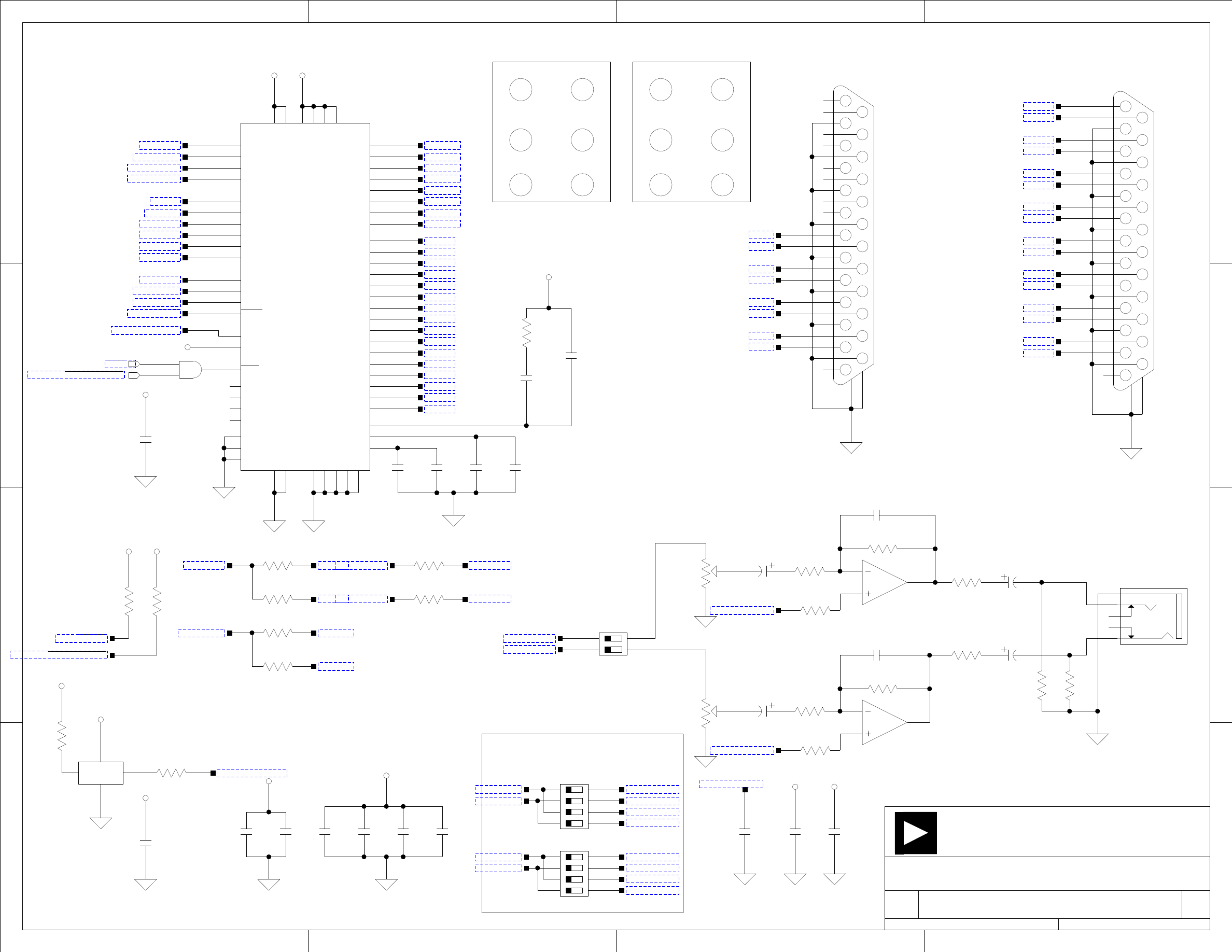
3.3V
ON
1
2
3
4
5V
3.3V
A3V
3.3V
3.3V
3.3V
3.3V
3.3V
A3V
A3V
1
2
ON
5V
ON
1
2
3
4
ABCLK
ADC1LN
ADC1LP
ADC1RN
ADC1RP
ADC2LN
ADC2LP
ADC2RN
ADC2RP
AGND1
AGND2
AGND3
AGND4
AGND5
ALRCLK
ASDATA1
ASDATA2
AVDD1
AVDD2
AVDD3
AVDD4
CCLK
CIN
CM
COUT
DBCLK
DGND1
DGND2
DLRCLK
DSDATA1
DSDATA2
DSDATA3
DSDATA4
DVDD1
DVDD2
FILTR
LF
MCLKI_XI
MCLKO_XO
NC1
NC2
NC3
NC4
OL1N
OL1P
OL2N
OL2P
OL3N
OL3P
OL4N
OL4P
OR1N
OR1P
OR2N
OR2P
OR3N
OR3P
OR4N
OR4P
VDRIVE
VSENSE
VSUPPLY
CLATCH
RESET
GND
OE
OUT
VDD
D
4
3
2
1
A
B
C
20 Cotton Road
Nashua, NH 03063
A
B
C
D
4
3
2
1
PH: 1-800-ANALOGD
C
Title
Size
Board No.
Date
Sheet
of
DEVICES
ANALOG
Rev
A0221-2008
ADSP-21469 EZ-BOARD
0.2
WHITE (LEFT)
RED (RIGHT)
3
4
9
10
6
5
5
6
10
9
4
3
AD1939 OSC
AD1939 OSC
HEADPHONE OUT (SHARED WITH OUT3/DAC5&6)
DEFAULT: ALL OFF
FOR TESTING PURPOSES ONLY
LOOPBACK CONNECTOR
RED (RIGHT)
WHITE (LEFT)
IN1 (L)
IN1 (R)
OUT3 (L)
OUT3 (R)
OUT1 (R)
PIN NUMBER FOR THE RESPECTIVE CONNECTOR.
NOTE: THE NUMBER INSIDE EACH OF THE CIRCLES IS THE ACTUAL
IN2 (L)
IN2 (R)
OUT2 (L)
OUT2 (R)
OUT4 (L)
OUT4 (R)
J4
J5
OUT1 (L)
DB25 Female Connectors for Conversion to XLR Connectors
SW23: HEAD PHONE ENABLE
DEFAULT: ALL OFF
NOTE: A USER NEEDS TO TURN SWITCH SW23
ON IN ORDER TO USE THE HEAD PHONE CONNECTOR.
8
16
3-31-2009_14:45
AUDIO PAGE 1
1
4
3
2
U12
12.288MHZ
OSC003
1
3
2
AD8397
SOIC_N8_EP
U51
1
4
3
2
5
J8
CON001
1
6
2
R493
RES_POT_DUAL
5K
1
4
48
46
44
33
16
17
32
5
45
51
62
14
2
3
34
30
31
35
28
29
27
26
21
22
20
19
18
15
47
52
61
49
63
64
50
23
24
25
54
53
56
55
58
57
60
59
37
36
39
38
41
40
43
42
7
6
9
8
11
10
13
12
U45
LQFP64
AD1939
1
10
11
12
13
14
15
16
17
18
19
2
20
21
22
23
24
25
26
27
3
4
5
6
7
8
9
P9
DB25F
9
8
7
6
5
4
3
27
26
25
24
23
22
21
20
2
19
18
17
16
15
14
13
12
11
10
1
P8
DB25F
0402
10.0K
R487
R488
10.0K
0402
R486
10.0K
0402
0402
33
R496
R495
33
0402
0402
33
R258
R263
33
0402
4
2
1
U50
SOT23-5
SN74LVC1G08
CT60
10UF
CAP002
CT59
10UF
CAP002
7
5
6
U51
SOIC_N8_EP
AD8397
2
3
1
4
5
6
7
8
SW24
DIP4
SWT018
4
5
3
R493
RES_POT_DUAL
5K
1
2
4
3
SW23
DIP2
SWT020
R484
100K
0402
0402
0
R492
AD1939_LF
AD1939_CM
TP9
0.01UF
0402
C142
0402
33
R262
0402
10K
R259
R257
33
0402
R261
33
0402
R260
10K
0402
C136
0402
0.01UF
0.01UF
0402
C137
0.01UF
0402
C138
C139
0402
0.01UF
0.01UF
0402
C140
C141
0402
0.01UF
5600PF
0805
C259
390PF
0603
C258
0603
562.0
R461
C257
10UF
0805
0603
0.1UF
C256
C255
0.1UF
0603
0805
10UF
C254
0402
10.0K
R491
0402
100.0
R490
R489
100.0
0402
C263
22PF
0805
C262
22PF
0805
CT58
47UF
ELEC_6MM
R485
0
0402
CT57
47UF
ELEC_6MM
100K
R483
0402
0.1UF
0402
C264
R494
10K
0402
C265
10UF
0805
8
7
6
5
4
1
3
2
SWT018
DIP4
SW25
0.01UF
0402
C266
C271
0402
0.1UF
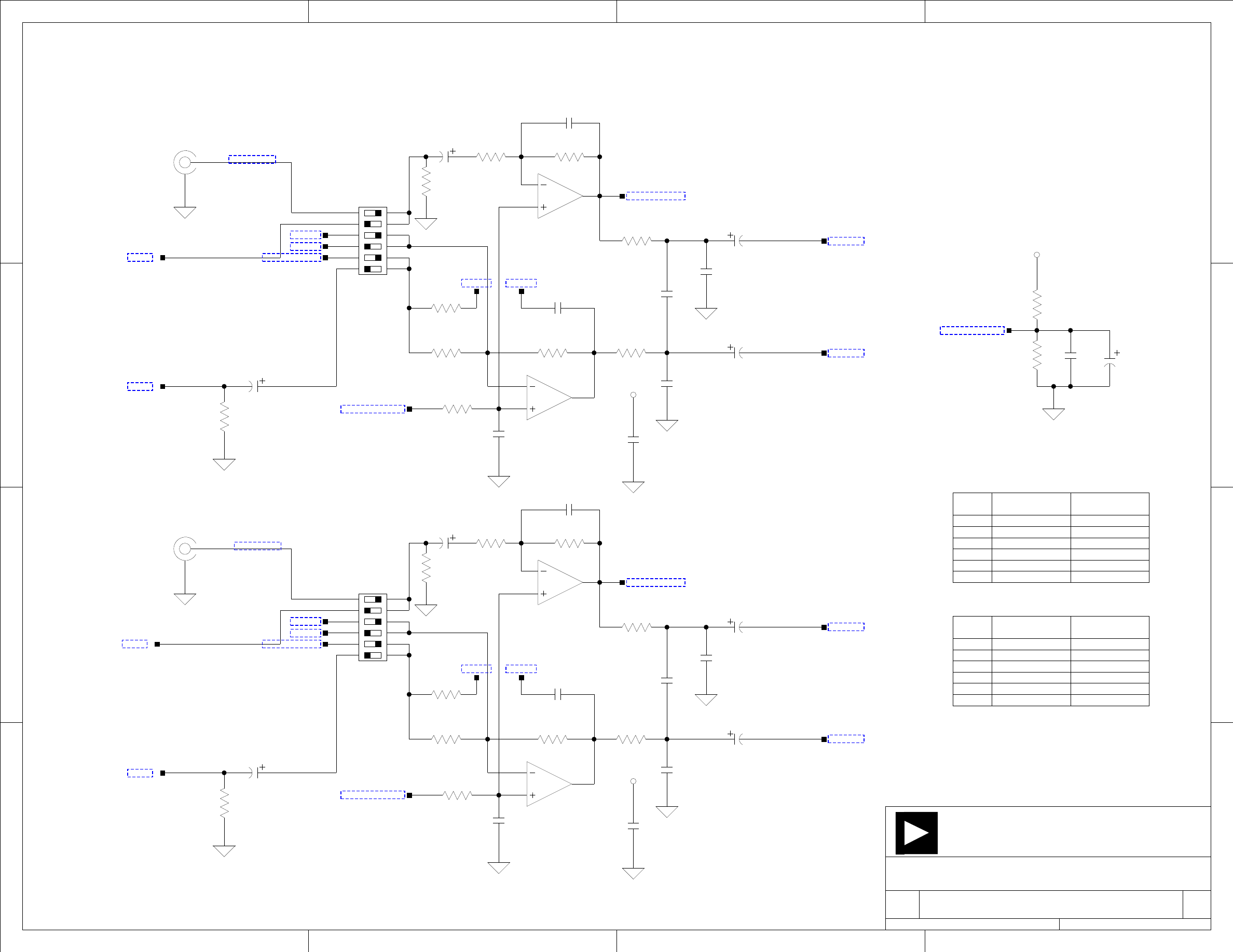
5V
1
2
4
5
6
ON
3
5V
5V
D
4
3
2
1
A
B
C
20 Cotton Road
Nashua, NH 03063
A
B
C
D
4
3
2
1
PH: 1-800-ANALOGD
C
Title
Size
Board No.
Date
Sheet
of
DEVICES
ANALOG
Rev
A0221-2008
ADSP-21469 EZ-BOARD
0.2
1
2
4
5
6
ON
3
OFF
ON
OFF
OFF
RCA IN (DEFAULT)
SINGLE ENDED USE
ON
ON
SWITCH
OFF
ON
OFF
ON
OFF
ON
ON
OFF
ON
OFF
ON
OFF
ON
ON
Bottom Left (White)
Bottom Right (Red)
IN1
SW15.1
SW15.2
SW15.3
SW15.4
SW15.5
SW15.6
SINGLE ENDED USE
RCA IN (DEFAULT)
OFF
OFF
ON
IN1 (LEFT) SETTINGS
IN1 (RIGHT) SETTINGS
SW16.1
SW16.2
SW16.3
SW16.4
SW16.5
SW16.6
NOTE: DIFFERENTIAL USE REQUIRES A DB25 TO XLR CABLE.
NOTE: DIFFERENTIAL USE REQUIRES A DB25 TO XLR CABLE.
OFF
DIFFERENTIAL USE
DB25 IN (P8)
DIFFERENTIAL USE
DB25 IN (P8)
SWITCH
ELEC_4MM
22UF
CT63
CT62
22UF
ELEC_4MM
R267
0603
237.0
CT1
ELEC_4MM
22UF
R286
806
0402
12
11
10
9
8
7
6
5
4
3
2
1
SWT017
DIP6
SW15
5.76K
0603
R281
22UF
ELEC_4MM
CT5
R266
0603
5.76K
R265
0603
49.9K
1
3
2
U20
SOIC_N8
AD8652ARZ
9
16
AUDIO PAGE 2
3-31-2009_14:34
2
5
J4
CON_RCA_6B
237.0
0603
R272
C161
10UF
0805
2
3
1
AD8652ARZ
SOIC_N8
U21
7
5
6
U20
SOIC_N8
AD8652ARZ
300PF
0603
C157
C148
0402
0.1UF
C145
0603
300PF
C147
0402
100PF
R274
0402
100.0
R268
0402
37.4K
C143
0603
300PF
R269
0603
5.76K
R273
0603
4.99K
R264
0603
4.99K
1
3
J4
CON_RCA_6B
R271
0603
49.9K
1000PF
0402
C150
0.1UF
0402
C151
CT3
ELEC_4MM
22UF
22UF
ELEC_4MM
CT6
C160
0402
0.1UF
C159
0402
1000PF
R285
0603
237.0
49.9K
0603
R284
1
2
3
4
5
6
7
8
9
10
11
12
SW16
DIP6
SWT017
237.0
0603
R280
4.99K
0603
R279
4.99K
0603
R278
5.76K
0603
R277
37.4K
0402
R276
100.0
0402
R275
100PF
0402
C155
300PF
0603
C153
0.1UF
0402
C152
7
5
6
U21
SOIC_N8
AD8652ARZ
R287
1.0K
0402
49.9K
0603
R282
CT61
100UF
C
C144
0402
1000PF
1000PF
0402
C154
ELEC_4MM
22UF
CT65
CT64
22UF
ELEC_4MM
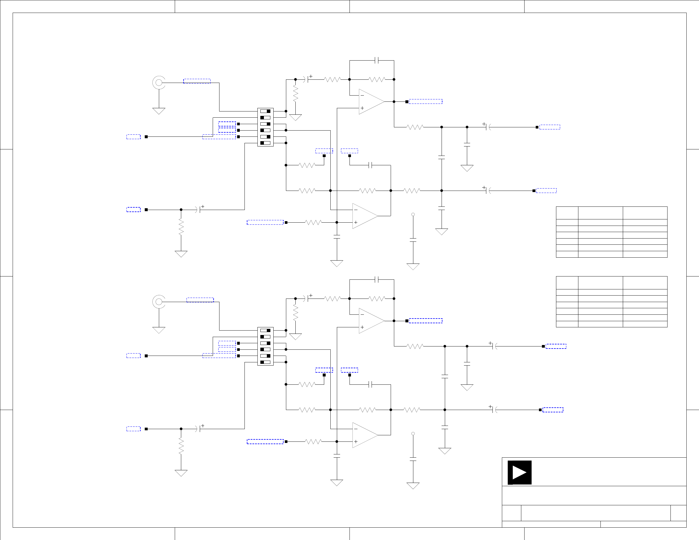
5V
1
2
4
5
6
ON
3
5V
D
4
3
2
1
A
B
C
20 Cotton Road
Nashua, NH 03063
A
B
C
D
4
3
2
1
PH: 1-800-ANALOGD
C
Title
Size
Board No.
Date
Sheet
of
DEVICES
ANALOG
Rev
A0221-2008
ADSP-21469 EZ-BOARD
0.2
1
2
4
5
6
ON
3
OFF
ON
OFF
OFF
RCA IN (DEFAULT)
SINGLE ENDED USE
ON
ON
SWITCH
OFF
ON
OFF
ON
OFF
ON
ON
OFF
ON
OFF
ON
OFF
ON
ON
SINGLE ENDED USE
RCA IN (DEFAULT)
OFF
OFF
ON
NOTE: DIFFERENTIAL USE REQUIRES A DB25 TO XLR CABLE.
NOTE: DIFFERENTIAL USE REQUIRES A DB25 TO XLR CABLE.
OFF
DIFFERENTIAL USE
DB25 IN (P8)
DIFFERENTIAL USE
DB25 IN (P8)
SWITCH
Bottom Left (White)
Bottom Right (Red)
IN2
IN2 (LEFT) SETTINGS
IN2 (RIGHT) SETTINGS
SW18.1
SW18.2
SW18.3
SW18.4
SW18.5
SW18.6
SW17.1
SW17.2
SW17.3
SW17.4
SW17.5
SW17.6
CT69
22UF
ELEC_4MM
ELEC_4MM
22UF
CT68
0.1UF
0402
C170
22UF
ELEC_4MM
CT9
1
2
3
4
5
6
7
8
9
10
11
12
SW17
DIP6
SWT017
5.76K
0603
R294
22UF
ELEC_4MM
CT8
R303
0603
5.76K
CT11
ELEC_4MM
22UF
10
16
3-31-2009_14:34
AUDIO PAGE 3
2
5
J5
CON_RCA_6B
1
3
J5
CON_RCA_6B
6
5
7
AD8652ARZ
SOIC_N8
U23
1
3
2
U23
SOIC_N8
AD8652ARZ
7
5
6
U22
SOIC_N8
AD8652ARZ
300PF
0603
C179
C178
0402
0.1UF
C177
0603
300PF
C175
0402
100PF
R309
0402
100.0
R308
0402
37.4K
C173
0603
300PF
R307
0603
5.76K
R306
0603
4.99K
R305
0603
4.99K
R304
0603
237.0
12
11
10
9
8
7
6
5
4
3
2
1
SWT017
DIP6
SW18
R300
0603
49.9K
237.0
0603
R299
1000PF
0402
C171
CT10
ELEC_4MM
22UF
C169
0402
0.1UF
C168
0402
1000PF
R298
0603
237.0
49.9K
0603
R297
237.0
0603
R293
4.99K
0603
R292
4.99K
0603
R291
5.76K
0603
R290
37.4K
0402
R289
100.0
0402
R288
100PF
0402
C165
300PF
0603
C163
0.1UF
0402
C162
1
3
2
U22
SOIC_N8
AD8652ARZ
R302
0603
49.9K
49.9K
0603
R295
1000PF
0402
C164
C176
0402
1000PF
ELEC_4MM
22UF
CT67
CT66
22UF
ELEC_4MM
5V
5V
5V
D
4
3
2
1
A
B
C
20 Cotton Road
Nashua, NH 03063
A
B
C
D
4
3
2
1
PH: 1-800-ANALOGD
C
Title
Size
Board No.
Date
Sheet
of
DEVICES
ANALOG
Rev
A0221-2008
ADSP-21469 EZ-BOARD
0.2
Middle Right (Red)
MIddle Left (White)
OUT1
R330
0603
6.81K
6.81K
0603
R329
R339
0603
6.81K
6.81K
0603
R312
100K
0402
R475
CT49
22UF
ELEC_4MM
R343
0603
49.9K
1
J4
CON_RCA_6B
6
7
5
U25
SOIC_N8
AD8652ARZ
11
16
3-19-2009_12:57
AUDIO PAGE 4
2
6
J4
CON_RCA_6B
2
3
1
AD8652ARZ
SOIC_N8
U26
1
3
2
U24
SOIC_N8
AD8652ARZ
2
1
3
U25
SOIC_N8
AD8652ARZ
6
7
5
U26
SOIC_N8
AD8652ARZ
6
7
5
U24
SOIC_N8
AD8652ARZ
R336
0603
49.9K
49.9K
0603
R310
R340
0402
100.0
R332
0402
100.0
100.0
0402
R333
100.0
0402
R331
R342
0603
4.99K
4.99K
0603
R327
R328
0603
4.99K
4.99K
0603
R311
C180
ELEC_5MM
22UF
R324
0603
4.99K
4.99K
0603
R314
R321
0402
750.0
C186
0402
620PF
620PF
0402
C181
2.43K
0402
R323
R319
0402
2.43K
750.0
0402
R317
680PF
0402
C182
2.67K
0402
R316
R320
0402
750.0
2.43K
0402
R315
R325
0402
2.43K
R338
0402
2.67K
C193
0402
680PF
R341
0402
750.0
C184
ELEC_5MM
22UF
C192
0402
620PF
R313
0603
4.99K
ELEC_4MM
22UF
CT16
CT14
22UF
ELEC_4MM
ELEC_4MM
22UF
CT19
CT18
22UF
ELEC_4MM
C183
0402
680PF
R318
0402
2.67K
R322
0402
2.67K
C185
0402
680PF
620PF
0402
C187
4.99K
0603
R326
100.0
0402
R334
100.0
0402
R335
49.9K
0603
R337
0.1UF
0402
C188
C189
0402
0.1UF
0.1UF
0402
C191
100K
0402
R476
CT50
22UF
ELEC_4MM
C267
0402
0.1UF
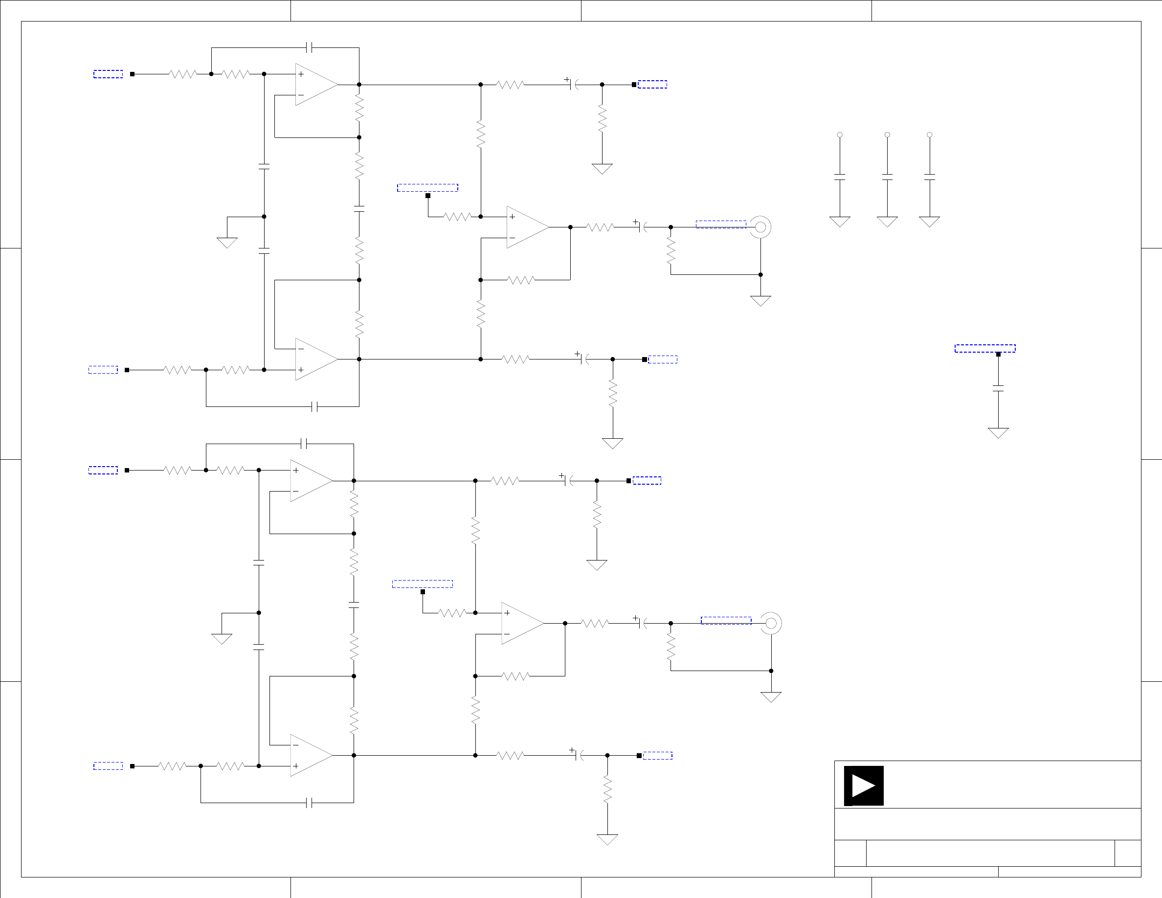
5V
5V
5V
D
4
3
2
1
A
B
C
20 Cotton Road
Nashua, NH 03063
A
B
C
D
4
3
2
1
PH: 1-800-ANALOGD
C
Title
Size
Board No.
Date
Sheet
of
DEVICES
ANALOG
Rev
A0221-2008
ADSP-21469 EZ-BOARD
0.2
MIddle Left (White)
Middle Right (Red)
OUT2
R365
0603
6.81K
6.81K
0603
R356
R355
0603
6.81K
6.81K
0603
R370
2
6
J5
CON_RCA_6B
6
7
5
U29
SOIC_N8
AD8652ARZ
12
16
3-19-2009_12:57
AUDIO PAGE 5
1
J5
CON_RCA_6B
3
1
2
AD8652ARZ
SOIC_N8
U29
1
3
2
U30
SOIC_N8
AD8652ARZ
6
7
5
U30
SOIC_N8
AD8652ARZ
1
3
2
U28
SOIC_N8
AD8652ARZ
6
7
5
U28
SOIC_N8
AD8652ARZ
0.1UF
0402
C200
C199
0402
0.1UF
C197
0402
0.1UF
R364
0603
49.9K
49.9K
0603
R363
R361
0402
100.0
R360
0402
100.0
100.0
0402
R359
100.0
0402
R358
R357
0603
4.99K
4.99K
0603
R354
R353
0603
4.99K
4.99K
0603
R352
C196
ELEC_5MM
22UF
R350
0603
4.99K
4.99K
0603
R349
R348
0402
750.0
C195
0402
620PF
620PF
0402
C194
2.43K
0402
R347
R346
0402
2.43K
750.0
0402
R345
680PF
0402
C207
2.67K
0402
R377
R376
0402
750.0
2.43K
0402
R375
R374
0402
2.43K
R373
0402
2.67K
C206
0402
680PF
R372
0402
750.0
C205
ELEC_5MM
22UF
C204
0402
620PF
R371
0603
4.99K
R369
0603
49.9K
ELEC_4MM
22UF
CT28
CT27
22UF
ELEC_4MM
ELEC_4MM
22UF
CT24
CT23
22UF
ELEC_4MM
C203
0402
680PF
R368
0402
2.67K
R367
0402
2.67K
C202
0402
680PF
620PF
0402
C201
4.99K
0603
R366
100.0
0402
R362
100.0
0402
R351
49.9K
0603
R344
ELEC_4MM
22UF
CT51
R477
0402
100K
ELEC_4MM
22UF
CT52
R478
0402
100K
C268
0402
0.1UF
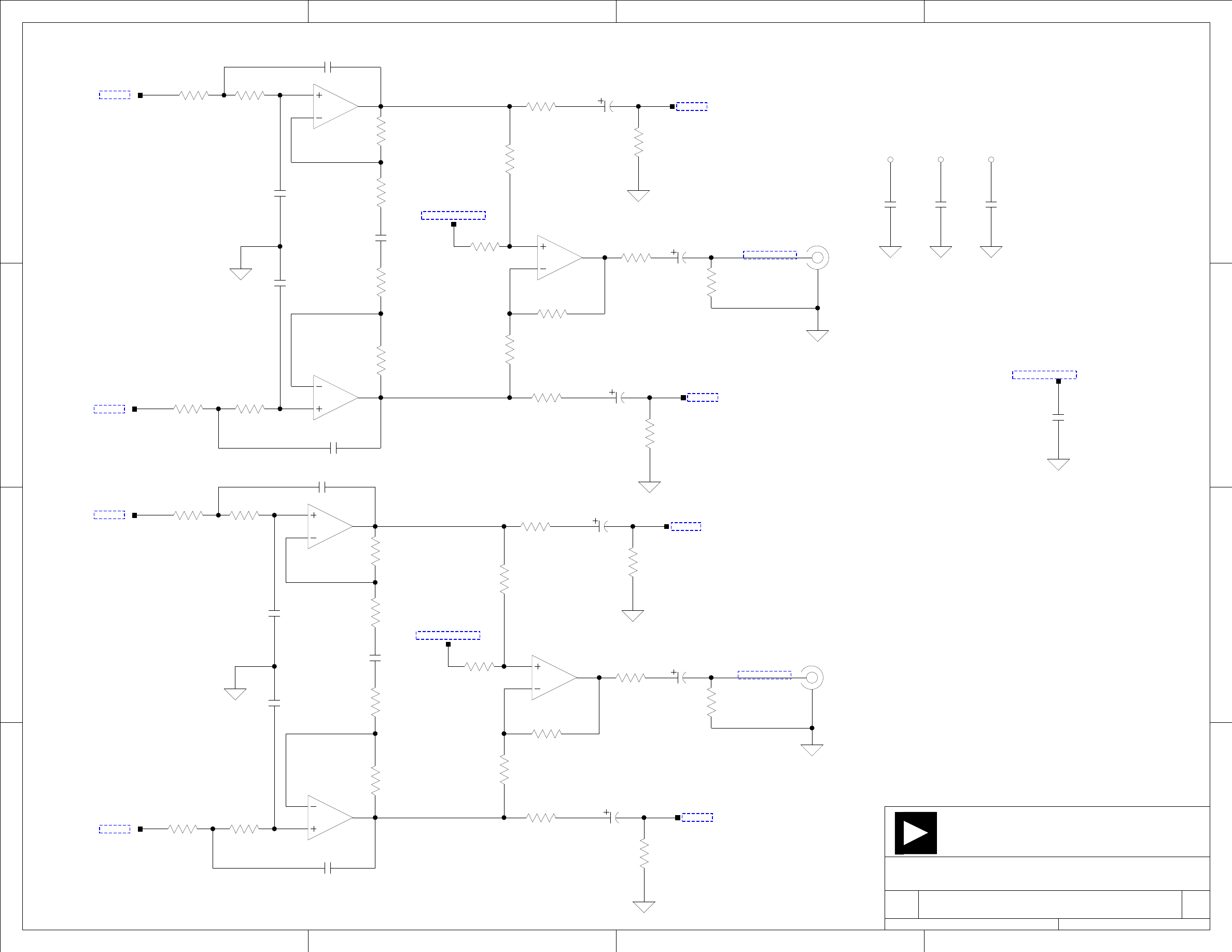
5V
5V
5V
D
4
3
2
1
A
B
C
20 Cotton Road
Nashua, NH 03063
A
B
C
D
4
3
2
1
PH: 1-800-ANALOGD
C
Title
Size
Board No.
Date
Sheet
of
DEVICES
ANALOG
Rev
A0221-2008
ADSP-21469 EZ-BOARD
0.2
OUT3
Top Right (Red)
Top Left (White)
R399
0603
6.81K
6.81K
0603
R390
R389
0603
6.81K
6.81K
0603
R404
R479
0402
100K
ELEC_4MM
22UF
CT53
C210
ELEC_5MM
22UF
C219
ELEC_5MM
22UF
6
7
5
U33
SOIC_N8
AD8652ARZ
13
16
3-19-2009_12:57
AUDIO PAGE 6
8
J4
CON_RCA_6B
7
9
J4
CON_RCA_6B
1
3
2
U34
SOIC_N8
AD8652ARZ
1
3
2
U32
SOIC_N8
AD8652ARZ
6
7
5
U34
SOIC_N8
AD8652ARZ
6
7
5
U32
SOIC_N8
AD8652ARZ
2
1
3
U33
SOIC_N8
AD8652ARZ
0.1UF
0402
C214
C213
0402
0.1UF
C211
0402
0.1UF
R398
0603
49.9K
49.9K
0603
R397
R395
0402
100.0
R394
0402
100.0
100.0
0402
R393
100.0
0402
R392
R391
0603
4.99K
4.99K
0603
R388
R387
0603
4.99K
4.99K
0603
R386
R384
0603
4.99K
4.99K
0603
R383
R382
0402
750.0
C209
0402
620PF
620PF
0402
C208
2.43K
0402
R381
R380
0402
2.43K
750.0
0402
R379
680PF
0402
C221
2.67K
0402
R411
R410
0402
750.0
2.43K
0402
R409
R408
0402
2.43K
R407
0402
2.67K
C220
0402
680PF
R406
0402
750.0
C218
0402
620PF
R405
0603
4.99K
R403
0603
49.9K
ELEC_4MM
22UF
CT36
CT35
22UF
ELEC_4MM
ELEC_4MM
22UF
CT32
CT31
22UF
ELEC_4MM
C217
0402
680PF
R402
0402
2.67K
R401
0402
2.67K
C216
0402
680PF
620PF
0402
C215
4.99K
0603
R400
100.0
0402
R396
100.0
0402
R385
49.9K
0603
R378
ELEC_4MM
22UF
CT54
R480
0402
100K
C269
0402
0.1UF
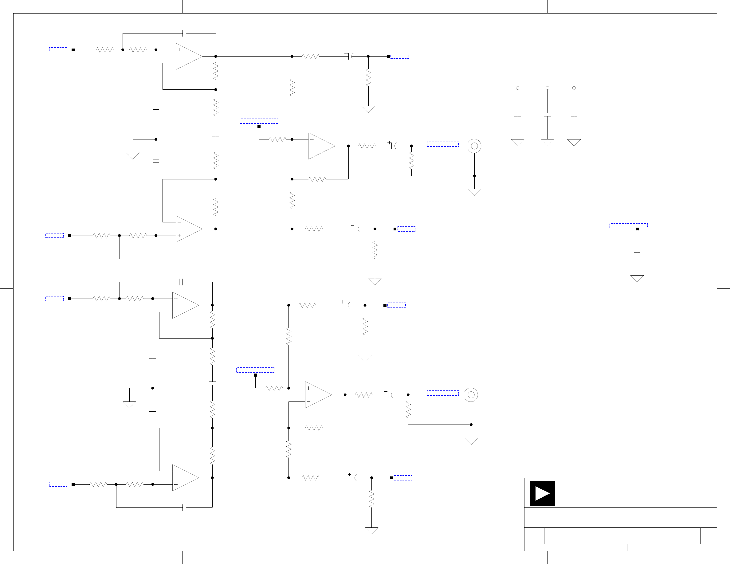
5V
5V
5V
D
4
3
2
1
A
B
C
20 Cotton Road
Nashua, NH 03063
A
B
C
D
4
3
2
1
PH: 1-800-ANALOGD
C
Title
Size
Board No.
Date
Sheet
of
DEVICES
ANALOG
Rev
A0221-2008
ADSP-21469 EZ-BOARD
0.2
Top Right (Red)
Top Left (White)
OUT4
C270
0402
0.1UF
R433
0603
6.81K
6.81K
0603
R424
R423
0603
6.81K
6.81K
0603
R438
6
7
5
U37
SOIC_N8
AD8652ARZ
14
16
3-19-2009_12:57
AUDIO PAGE 7
8
J5
CON_RCA_6B
1
3
2
U38
SOIC_N8
AD8652ARZ
6
7
5
U38
SOIC_N8
AD8652ARZ
1
3
2
U36
SOIC_N8
AD8652ARZ
6
7
5
U36
SOIC_N8
AD8652ARZ
2
1
3
U37
SOIC_N8
AD8652ARZ
0.1UF
0402
C228
C227
0402
0.1UF
C225
0402
0.1UF
R432
0603
49.9K
49.9K
0603
R431
R429
0402
100.0
R428
0402
100.0
100.0
0402
R427
100.0
0402
R426
R425
0603
4.99K
4.99K
0603
R422
R421
0603
4.99K
4.99K
0603
R420
C224
ELEC_5MM
22UF
R418
0603
4.99K
4.99K
0603
R417
R416
0402
750.0
C223
0402
620PF
620PF
0402
C222
2.43K
0402
R415
R414
0402
2.43K
750.0
0402
R413
680PF
0402
C235
2.67K
0402
R445
R444
0402
750.0
2.43K
0402
R443
R442
0402
2.43K
R441
0402
2.67K
C234
0402
680PF
R440
0402
750.0
C233
ELEC_5MM
22UF
C232
0402
620PF
R439
0603
4.99K
R437
0603
49.9K
ELEC_4MM
22UF
CT44
CT43
22UF
ELEC_4MM
ELEC_4MM
22UF
CT40
CT39
22UF
ELEC_4MM
C231
0402
680PF
R436
0402
2.67K
R435
0402
2.67K
C230
0402
680PF
620PF
0402
C229
4.99K
0603
R434
100.0
0402
R430
100.0
0402
R419
49.9K
0603
R412
7
9
J5
CON_RCA_6B
ELEC_4MM
22UF
CT55
R481
0402
100K
ELEC_4MM
22UF
CT56
R482
0402
100K
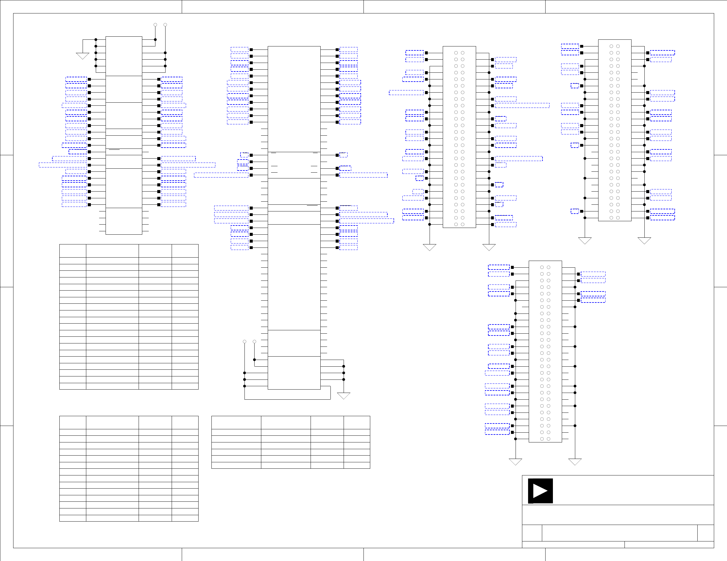
5V
3.3V
3.3V
CLK1+
CLK1-
CLK2+
CLK2-
D0
D1
D10
D11
D12
D13
D14
D15
D16
D17
D18
D19
D2
D20
D21
D22
D23
D24
D25
D26
D27
D28
D29
D3
D30
D31
D4
D5
D6
D7
D8
D9
GND0
GND1
GND10
GND11
GND12
GND13
GND14
GND15
GND16
GND17
GND2
GND3
GND4
GND5
GND6
GND7
GND8
GND9
CLK1+
CLK1-
CLK2+
CLK2-
D0
D1
D10
D11
D12
D13
D14
D15
D16
D17
D18
D19
D2
D20
D21
D22
D23
D24
D25
D26
D27
D28
D29
D3
D30
D31
D4
D5
D6
D7
D8
D9
GND0
GND1
GND10
GND11
GND12
GND13
GND14
GND15
GND16
GND17
GND2
GND3
GND4
GND5
GND6
GND7
GND8
GND9
5V
D
4
3
2
1
A
B
C
20 Cotton Road
Nashua, NH 03063
A
B
C
D
4
3
2
1
PH: 1-800-ANALOGD
C
Title
Size
Board No.
Date
Sheet
of
DEVICES
ANALOG
Rev
A0221-2008
ADSP-21469 EZ-BOARD
0.2
3.3V1
3.3V2
ACK
ADDR0
ADDR1
ADDR10
ADDR11
ADDR12
ADDR13
ADDR14
ADDR15
ADDR16
ADDR17
ADDR18
ADDR19
ADDR2
ADDR20
ADDR21
ADDR22
ADDR23
ADDR24
ADDR25
ADDR26
ADDR27
ADDR28
ADDR29
ADDR3
ADDR30
ADDR31
ADDR4
ADDR5
ADDR6
ADDR7
ADDR8
ADDR9
CLKOUT
DATA0
DATA1
DATA10
DATA11
DATA12
DATA13
DATA14
DATA15
DATA16
DATA17
DATA18
DATA19
DATA2
DATA20
DATA21
DATA22
DATA23
DATA24
DATA25
DATA26
DATA27
DATA28
DATA29
DATA3
DATA30
DATA31
DATA4
DATA5
DATA6
DATA7
DATA8
DATA9
FLAG0
FLAG1
FLAG2
FLAG3
GND1
GND2
GND3
GND4
PWR_IN1
PWR_IN2
RSVD1
RSVD10
RSVD11
RSVD12
RSVD13
RSVD14
RSVD15
RSVD16
RSVD17
RSVD2
RSVD3
RSVD4
RSVD5
RSVD6
RSVD7
RSVD8
RSVD9
VDDIO1
VDDIO2
MS0
MS1
MS2
MS3
RD
RESET
WR
3.3V1
3.3V2
DAI1
DAI10
DAI11
DAI12
DAI13
DAI14
DAI15
DAI16
DAI17
DAI18
DAI19
DAI2
DAI20
DAI3
DAI4
DAI5
DAI6
DAI7
DAI8
DAI9
DPI1
DPI10
DPI11
DPI12
DPI13
DPI14
DPI2
DPI3
DPI4
DPI5
DPI6
DPI7
DPI8
DPI9
FLAG0
FLAG1
FLAG2
FLAG3
GND1
GND2
GND3
GND4
GND5
GND6
NC
PWR_IN1
PWR_IN2
RSVD1
RSVD2
RSVD3
RSVD4
RSVD5
RSVD6
RSVD7
RSVD8
VDDIO1
VDDIO2
RESET
CLK1+
CLK1-
CLK2+
CLK2-
D0
D1
D10
D11
D12
D13
D14
D15
D16
D17
D18
D19
D2
D20
D21
D22
D23
D24
D25
D26
D27
D28
D29
D3
D30
D31
D4
D5
D6
D7
D8
D9
GND0
GND1
GND10
GND11
GND12
GND13
GND14
GND15
GND16
GND17
GND2
GND3
GND4
GND5
GND6
GND7
GND8
GND9
PERIPHERAL ON THE EZ-BOARD.
NOTE: SHUTTING OFF ANY OF THE SWITCHES FOR EXPANSION USE
FLASH_CS
ON
ON
CONNECTED
CONNECTED TO
PERIPHERAL NET
VIA SWITCH
DEFAULT
SWITCH
ON
ON
ON
SWITCH
DEFAULT
PERIPHERAL NET
CONNECTED TO
NAME
DSP PIN
ON
ON
ON
ON
ON
ON
ON
ON
ON
ON
ON
ON
ON
ON
ON
ON
ON
ON
ON
ON
ON
ON
ON
ON
LED8
DSP PIN
NAME
DAI_P1
DAI_P2
DAI_P3
DAI_P4
DAI_P5
DAI_P6
DAI_P7
DAI_P8
DAI_P9
DAI_P10
DAI_P11
DAI_P12
DAI_P13
DAI_P14
DAI_P15
DAI_P16
DAI_P17
DAI_P18
DAI_P19
DAI_P20
LED4
ASDATA1
ASDATA2
ABCLK
ALRCLK
DSDATA4
DSDATA3
DSDATA2
DSDATA1
DBCLK
DLRCLK
LED5
LED6
LED7
SPDIF_IN
PB3
PB4
SW1.2
SW1.3
SW1.4
SW1.5
SW1.6
SW1.7
SW1.8
SW2.5
SW2.6
SW2.7
SW2.8
SW2.1
SW2.2
SW2.3
SW2.4
SW7.1
SW7.2
SW7.3
SW7.4
DEFAULT
SWITCH
SW1.1
ON
ON
OFF
OFF
DPI_P1
DPI_P2
DPI_P3
DPI_P4
DPI_P5
DPI_P6
DPI_P7
DPI_P8
DPI_P9
DPI_P10
DPI_P11
DPI_P12
DPI_P13
DPI_P14
SPI_MOSI
SPI_MISO
SPI_CLK
AD1939_CS
SPI_CS
LED1
TEMP_SDA
TEMP_SCK
UART_TX
UART_RX
UART_RTS
UART_CTS
LED2
LED3
SW3.1
SW3.2
SW3.3
SW3.4
SW3.5
SW3.6
SW3.7
SW3.8
SW14.1
SW14.2
SW14.3
SW14.4
SW14.5
SW14.6
ON
ON
OFF
OFF
FLAG2/IRQ2/MS2
FLAG3/TIMEXP/MS3
FLASH_CS
TEMP_THERM
PB1
PB2
TEMP_IRQ
SW13.1
SW13.2
SW13.3
SW13.4
SW13.5
SW13.6
OFF
OFF
OFF
NOTE: SHUTTING OFF ANY OF THE SWITCHES FOR EXPANSION USE
WILL CAUSE LOSS OF FUNCTIONALITY TO THE RESPECTIVE
PERIPHERAL ON THE EZ-BOARD.
PERIPHERAL NET
CONNECTED TO
SPDIF_OUT
AD1939_SOFT_RESET
VIA SWITCH
CONNECTED
NOTE: SHUTTING OFF ANY OF THE SWITCHES FOR EXPANSION USE
WILL CAUSE LOSS OF FUNCTIONALITY TO THE RESPECTIVE
PERIPHERAL ON THE EZ-BOARD.
DSP PIN
NAME
MS0
MS1
FLAG0/IRQ0
FLAG1/IRQ1
CONNECTED
VIA SWITCH
WILL CAUSE LOSS OF FUNCTIONALITY TO THE RESPECTIVE
B23
B24
B25
B26
B27
B22
B21
B20
B19
B18
B17
B16
B15
B14
B13
B12
B11
B10
B9
B8
B7
A27
A26
A25
A24
A23
A22
A21
A20
A19
A18
A17
A16
A15
A14
A13
A12
A11
A10
A9
A8
A7
A6
A5
A4
A2
A3
A1
B6
B5
B4
B3
B2
B1
P6
DMAX_ALT
DNP
57
55
53
51
59
60
58
56
54
10
12
14
16
1
3
5
7
9
11
38
40
36
20
18
42
44
46
48
30
21
23
26
19
28
34
32
2
4
6
8
50
49
22
24
13
17
15
25
27
29
31
33
35
37
39
41
43
45
47
52
P2
IDC30X2_SMTA
87
88
104
99
95
98
101
102
100
103
92
94
90
96
89
91
93
97
79
75
73
71
78
72
76
74
85
82
84
83
80
77
81
86
70
65
61
64
67
68
66
69
11
35
36
1
3
5
7
4
6
18
16
17
28
27
30
29
32
31
34
33
20
19
22
21
24
23
26
25
13
14
15
42
54
58
60
52
38
40
44
46
48
50
56
39
41
43
45
47
51
37
2
9
10
12
8
62
49
55
53
57
59
63
J1
QMS52X2_SMT
15
16
3-31-2009_14:34
EXPANSION II INTERFACE / L.A. CONNECTORS
B23
B24
B25
B26
B27
B22
B21
B20
B19
B18
B17
B16
B15
B14
B13
B12
B11
B10
B9
B8
B7
A27
A26
A25
A24
A23
A22
A21
A20
A19
A18
A17
A16
A15
A14
A13
A12
A11
A10
A9
A8
A7
A6
A5
A4
A2
A3
A1
B6
B5
B4
B3
B2
B1
P7
DMAX_ALT
DNP
B1
B2
B3
B4
B5
B6
A1
A3
A2
A4
A5
A6
A7
A8
A9
A10
A11
A12
A13
A14
A15
A16
A17
A18
A19
A20
A21
A22
A23
A24
A25
A26
A27
B7
B8
B9
B10
B11
B12
B13
B14
B15
B16
B17
B18
B19
B20
B21
B22
B27
B26
B25
B24
B23
P5
DMAX_ALT
DNP
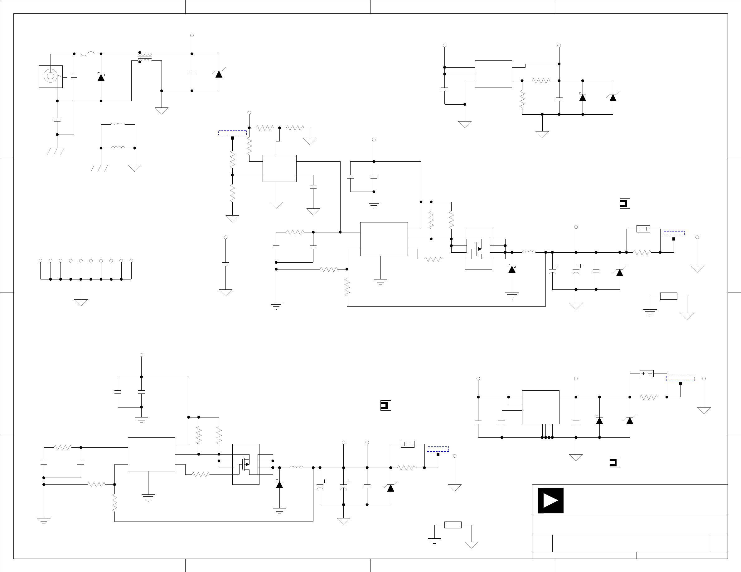
5V
5V
PGND2
PGND2
PGND2
PGND2
PGND
PGND
PGND
JUMPER
SHORTING
3.3V
JUMPER
SHORTING
SHGND
SHGND
POWER
5V
3.3V
5V
PGND
PGND
PGND2
D
4
3
2
1
A
B
C
20 Cotton Road
Nashua, NH 03063
A
B
C
D
4
3
2
1
PH: 1-800-ANALOGD
C
Title
Size
Board No.
Date
Sheet
of
DEVICES
ANALOG
Rev
A0221-2008
ADSP-21469 EZ-BOARD
0.2
A3V
IN
EN
GND
OUT
ADJ
GND4
GND3
GND2
EN
OUT
GND1
IN
SS
COPPER
COPPER
JUMPER
SHORTING
5V
GND
EN_OUT
CEXT
VDD
VIN
EN_IN
IN
CS
PGATE
FB
COMP
GND
IN
CS
PGATE
FB
COMP
GND
5V
LABEL "GND" ON ALL TPs
"5V"
"VDD_DDR2"
3.3V @ 2A
1.8V @ 500mA
"VDDEXT"
1.1V @ 2A
Remove P14 when measuring VDDINT
ANALOG AUDIO (AD1939) POWER
Remove P13 when measuring VDD_DDR2
GND Test Points are scattered on PCB for Test Measurement Purposes.
Remove P15 when measuring VDDEXT
D10
30A
GSOT03
SOT23-3
D8
40A
ESD5Z2.5T1
SOD-523
D9
7A
VESD01-02V-GS08
SOD-523
SOT23-3
GSOT03
30A
D7
SOT23-3
GSOT05
30A
D6
R502
8.20K
0603
0402
4.7K
R501
R498
0
0402
R458
0
0603
R499
10.0K
0402
0402
16.9K
R500
2
6
3
1
5
4
VR2
ADP1864AUJZ
SOT23-6
2
6
3
1
5
4
VR3
ADP1864AUJZ
SOT23-6
D4
1A
SK12
DO-214AA
0402
10000PF
C272
DNP
3
2
1
4
5
6
U52
SC70_6
ADM1085
C249
68PF
0603
DEFAULT=INSTALLLED
SJ1
W1
4A
DO-214AA
SK12
1A
D5
1206
0.05
R446
C239
2.2UF
0805
D1
5A
MBRS540T3G
SMC
D3
5A
MBRS540T3G
SMC
D2
5A
MBRS540T3G
SMC
TP7
W2
4A
TP3
TP16
8
7
6
1
3
5
2
4
VR4
ADP1715
MSOP8
R453
30.9K
0402
R449
80.6K
0603
4
3
2
1
8
7
6
5
U15
SI7601DN
ICS010
4
3
2
1
8
7
6
5
U16
SI7601DN
ICS010
1206
0.036
R451
R450
0.036
1206
1206
0.036
R457
R456
0.036
1206
CT45
220UF
D2E
1
3
2
5
4
VR1
ADP1710
TSOT5
0402
10.0K
R474
0603
31.6K
R473
C261
1UF
0603
0603
1UF
C260
16
16
3-31-2009_14:34
POWER
R447
255.0K
0603
1
2
3
P16
CON045
4
1
3
2
FER9
FER002
190
C245
10UF
1210
F1
FUS005
5A
C236
1206
1000PF
C251
1206
1000PF
1206
FER8
600
FER7
1206
600
1
2
IDC2X1
P15
SJ3
DEFAULT=INSTALLLED
R460
0.05
1206
TP8
2
1
P13
IDC2X1
TP4
0805
2.2UF
C238
C237
0.1UF
0402
R452
0
0603
C244
10UF
1210
C243
68PF
0603
C242
470PF
0603
R448
24.9K
0603
C241
10UF
0805
DNP
L1
2.5UH
IND013
C240
4.7UF
0805
CT46
2.2UF
B
DNP
TP5
C250
10UF
1210
R455
80.6K
0603
C248
470PF
0603
R454
24.9K
0603
C247
10UF
0805
DNP
L2
2.5UH
IND013
C246
4.7UF
0805
CT48
2.2UF
B
DNP
CT47
470UF
D2E
TP6
1206
0.05
R459
DEFAULT=INSTALLLED
SJ2
2
1
P14
IDC2X1
TP19
TP18 TP17
TP15
TP14
TP13
TP12
TP11
TP10
C273
0402
0.1UF

ADSP-21469 EZ-Board Evaluation System Manual
I-1
I
INDEX
A
ABCLK signal,
,
AD1939 codec,
,
,
AD1939_CS signal,
ALRCLK signal,
analog audio interface, See audio
analog-to-digital converters (ADCs), See
AD1939 codec
architecture, of this EZ-Board,
ASDATA1-2 signals,
async control enable switch (SW13),
,
,
audio
codec, See also AD1939 codec
interface,
left select switch (SW15),
left select switch (SW18),
loopback switches (SW24-25),
RCA connectors (J4-5),
right select switch (SW16),
right select switch (SW17),
B
bill of materials,
board design database,
board schematic (ADSP-21469),
boot
modes,
mode select switch (SW4),
,
,
C
configuration, of this EZ-Board,
connectors
diagram of locations,
J1 (expansion interface II),
J2 (RS-232),
,
,
J4 (RCA),
J5 (RCA),
J6 (S/PDIF in),
J7 (S/PDIF out),
J8 (headphones),
,
P10 (MLB),
P12 (link port 0),
,
P13 (VDD_DDR2 power),
P15 (VDDEXT power),
P16 (5.0V wall adaptor),
P1 (JTAG),
,
P2 (expansion interface II),
P5-7 (DMAX land grid array),
P8-9 (diff in/out),

Index
I-2
ADSP-21469 EZ-Board Evaluation System Manual
contents, of this EZ-Board package,
core voltage,
D
DAI_P1-2 pins,
DAI_P15-17 pins,
DAI_P19-20 pins,
,
DAI_P3-4 pins,
DAI_P5-14 pins,
DB25 connector,
,
DBCLK signal,
,
,
debug agent connector (ZP1),
default configuration, of this EZ-Board,
differential on/out connectors (P8-9),
digital audio interface (DAI)
LED connections,
SW1 switch,
SW2 switch,
SW7 switch,
,
digital peripheral interface (DPI)
LED connections,
SPI memory connections,
SW14 switch,
SW3 switch,
,
digital-to-analog converters (DACs), See
AD1939 codec
DLRCLK signal,
,
,
double data rate (DDR2) memory,
DPI_13-14 pins,
DPI_P6 pin,
DSP clock config switch (SW5),
E
evaluation license
expansion interface II
J1 connector,
P2 connector,
F
features, of this EZ-Board,
FLASH_CS singal,
flash WP jumper (JP1),
G
general-purpose IO pins (GPIO),
,
H
headphones
enable switch (SW23),
,
I
installation, of this EZ-Board,
Integrated Interchip Sound (I2C) mode,
internal memory space,
IO voltage,
,

ADSP-21469 EZ-Board Evaluation System Manual
I-3
Index
J
J3 (link port 0) connector,
,
J8 (headphones) connector,
JTAG,
interface,
,
SW19-22 switches,
,
jumpers
diagram of locations,
JP2 (S/PDIF loopback),
JP3 (UART RTS/CTS),
JP4 (UART loopback),
P14 (VDDEXT power),
P15 (VDD_DDR2 power),
L
land grid array connectors (P5-7),
,
LEDs
diagram of locations,
LED11 (thermal limit),
LED1-8 (DAI, DPI),
LED1 (DPI_P6, SW3),
,
LED2 (DPI_P13, SW14),
,
LED3 (DPI_14, SW14),
,
LED4 (DAI_P3, SW1),
,
LED5 (DAI_P4, SW1),
,
LED6 (DAIP15, SW2),
,
LED7 (DAI_16, SW2),
LED8 (DAI_P17, SW7),
LED9 (power),
license restrictions,
link port
,
,
interface,
M
master input clock (MCLK),
media local bus (MLB) connector (P10),
MS0-1 select lines,
MS2-3 select lines,
multi-processor configuration,
N
notation conventions,
O
P
,
,
,
parallel flash memory,
,
,
PB1-2,
PB3-4,
POST (power-on-self test) program,
power
5V wall adaptor (P16),
,
,
LED (LED9),
measurements,
product information,
push buttons
connections,
SW8-11 (IO) switches,
,

Index
I-4
ADSP-21469 EZ-Board Evaluation System Manual
R
RCA audio connector
J4,
J5,
reset
LED (LED10),
push button (SW12),
RS-232 connector (J2),
S
schematic, of ADSP-21469 EZ-Board,
SDRAM interface,
serial clock signal (SCK),
serial data signal (SDA),
serial peripheral interconnect (SPI) ports,
See SPI interface
signal routing units
SRU2 (DPI interface),
SRU (DAI interface),
single-processor configuration,
SOFT_RESET signal,
SPDIF_IN signal,
,
S/PDIF interface
in connector (J6),
SPDIF_OUT signal,
,
SPI_CLK signal,
,
SPI_CS signal,
SPI interface,
,
SPI_MISO signal,
,
SPI_MOSI signal,
,
SRAM memory,
standalone debug agent,
,
startup, of this EZ-Board
CCES,
SW12 (reset) push button,
SW13 (async control enable),
,
,
,
SW14 (DPI 9-14 enable) switch,
SW15 (audio left select) switch,
SW16 (audio right select) switch,
SW17 (audio right select) switch,
SW18 (audio left select) switch,
SW19-22 (JTAG) switches,
SW1 (DAI 1-8 enable) switch,
SW23 (headphone enable) switch,
,
SW24-25 (audio loopback) switches,
SW2 (DAI 9-16 enable) switch,
SW4 (boot mode select) switch,
,
SW7 (DAI 17-20 enable) switch,
,
,
SW8-11 (IO) push buttons,
,
switches, diagram of locations,
system architecture, of this EZ-Board,
T
technical support,
,
TEMP_SDA signal,
temp sensor interface,
thermal limit LED (LED11),
time-division multiplexed (TDM) mode,

ADSP-21469 EZ-Board Evaluation System Manual
I-5
Index
U
UART
interface connections,
RTS/CTS jumper (JP3),
UART_CTS signal,
,
UART_RTS signal,
,
,
UART_RX signal,
,
UART_TX signal,
universal asynchronous receiver
transmitter, See UART
USB monitor LED (LED4),
V
VDD_DDR2
power connectors (P13),
voltage domain,
VDDEXT
power connector (P15),
voltage domain,
VDDINT
power connector (P14),
voltage domain,
voltage planes,
,
Document Outline
- ADSP-21469 EZ-Board Evaluation System Manual, Revision 1.1, July 2012
- Contents
- Preface
- 1 Using the ADSP-21469 EZ-Board
- Package Contents
- Default Configuration
- CCES Install and Session Startup
- VisualDSP++ Install and Session Startup
- CCES Evaluation License
- VisualDSP++ Evaluation License
- Memory Map
- DDR2 Interface
- Parallel Flash Memory Interface
- SPI Interface
- Link Port Interface
- Temperature Sensor Interface
- S/PDIF Interface
- Audio Interface
- UART Interface
- LEDs and Push Buttons
- JTAG Interface
- Land Grid Array
- Expansion Interface II
- Power Measurements
- Power-On-Self Test
- Example Programs
- Board Design Database
- 2 ADSP-21469 EZ-Board Hardware Reference
- System Architecture
- Flags and Memory Selects
- Push Button and Switch Settings
- DAI [1–8] Enable Switch (SW1)
- DAI [9–16] Enable Switch (SW2)
- DPI [1–8] Enable Switch (SW3)
- Boot Mode Select Switch (SW4)
- DSP Clock Configuration Switch (SW5)
- DAI [17–20] Enable Switch (SW7)
- Programmable Flag Push Buttons (SW8–11)
- Reset Push Button (SW12)
- Asynchronous Control Enable Switch (SW13)
- DPI [9–14] Enable Switch (SW14)
- Audio In1 Left Selection Switch (SW15)
- Audio In1 Right Selection Switch (SW16)
- Audio In2 Right Selection Switch (SW17)
- Audio In2 Left Selection Switch (SW18)
- JTAG Switches (SW19–22)
- Headphone Enable Switch (SW23)
- Audio Loopback Switches (SW24–25)
- Jumpers
- LEDs
- Connectors
- Expansion Interface II Connector (J1)
- RS-232 Connector (J2)
- Link Port 1 Connector (J3)
- RCA Audio Connector (J4)
- RCA Audio Connector (J5)
- S/PDIF IN Connector (J6)
- S/PDIF OUT Connector (J7)
- Headphone Out Connector (J8)
- JTAG Connector (P1)
- Expansion Interface II Connector (P2)
- DMAX Land Grid Array Connectors (P5–7)
- Differential In/Out Connectors (P8–9)
- MLB Connector (P10)
- Link Port 0 Connector (P12)
- VDD_DDR2 Power Connector (P13)
- VDDINT Power Connector (P14)
- VDDEXT Power Connector (P15)
- Power Connector (P16)
- Standalone Debug Agent Connector (ZP1)
- A ADSP-21469 EZ-Board Bill Of Materials
- B ADSP-21469 EZ-Board Schematic
- Title Page
- Processor - DDR2 Interface
- Processor - ASYNC Interface
- Processor - DAI, DPI, Link Port Interfaces
- Processor - Power
- S/PDIF, RS-232, JTAG Interfaces
- Reset Circuit, Push Buttons, LEDs
- Audio Page 1
- Audio Page 2
- Audio Page 3
- Audio Page 4
- Audio Page 5
- Audio Page 6
- Audio Page 7
- Expansion II Interface / L.A. Connectors
- Power
- I Index
Wyszukiwarka
Podobne podstrony:
ADSP 21467 21469
NP 003 Rev 0, ERP Man Overboard, STW
03 2000 Revisions Overview Rev 3 1 03
05 DFC 4 1 Sequence and Interation of Key QMS Processes Rev 3 1 03
400 man
man ar900
Przegląd układu tłokowo – korbowego silnika MAN B&W – L 2330 H
Procol Harum The Dead Man's Dream
43. de Man, teoria literatury!!!
In literary studies literary translation is a term of two meanings rev ag
ADSP 2186M 0
juma rx1 main SCH Rev E
man ar2700
MAN Ogrzewanie Webasto Thermo 230,300,350 obsługa i montaż(1)
Cheddar Man provisions of Oxford
czytanie koło II Man?out the House
Odd Man Out
więcej podobnych podstron