
1
Advantages
- is easy available renewable energy source (not necessary extraction, it's free)
- its use does not pollute the environment
- more even distribution in comparison with the world's reserves of conventional
and exhaustible fuels such as oil, coal and natural gas.
Disadvantages
- much lower energy density, due to the relatively low efficiency of energy
conversion
(for 1 MW photovoltaic power plant it is required about 2-3 ha)
.
- unstable availability
5.2 Possibilities of using sunlight for energy
Advantages and disadvantages of using solar radiation

2
There are several principles of conversion of
solar energy
into another form
of energy, the most common is the transformation into:
1) electricity
a) by direct form
- the principle is in the using of the photoelectric effect in
photovoltaic cells
,
which convert solar energy directly into electricity
b) by indirect form
- the principle is in converting solar energy into heat energy and subsequent
conversion by suitable devices (solar thermal) into electrical energy
- indirect conversion efficiency of solar energy is higher than that of photovoltaic
systems, so that we can achieve higher performance per unit area of solar
power.
2) thermal energy
- conversion of solar energy into heat energy by the
collector
(liquid, air)
Principles of conversion solar energy into another form

3
5.2.1 The conversion of solar energy into electricity by direct form -
solar power plants
Photovoltaic (solar) cell
is a large semiconductor device that converts solar energy
directly into electricity using the
photoelectric effect.
Photovoltaic cells have many applications. They are used for feeding of the small
devices (eg calculators, chargers, lights, ...) in the space industry (artificial satellite)
and also in large are being used in the energy industry.

4
Photoelectric effect - historical development
The first experiments in which the observed photoelectric effect
will be taken by a French physicist Mr. Becquerel in 1839.
The FV cell was based on metal electrodes immersed in the
electrolyte. When exposed to sunlight observed increase tension
on them.
- the further development of PV technologies have a major impact
theoretical clarification of the photoelectric effect by Albert Einstein
in 1905
- for the technology of modern silicon cells was an important the
discovery of method for production of pure monocrystalline silicon
developed by Mr. Jan Czochralski in 1916
http://www.eia.gov/kids/energy.cfm?page=tl_photovoltaic
- in 1877 Mr. Adams and Mr. Day, produced the first solid photovoltaic cell from selenium
- In 1883 Mr. Fritts produced the cel with efficiency 1 %

5
Photoelectric effect - historical development
- in the middle of 50th years of 20ht century started the development of semiconductors.
Essential element for the production of semiconductor materials is silicon, that is on the
surface in large quantities.
- in 1954 was created the first silicon (Si) photovoltaic panel with P-N junction with
efficiency 7 %
- first real energy sources on the principle of direct conversion of solar energy into
electricity were produced in the years 1955-58 and used for satellite Sputnik and
Avantgard
- PV cells was first time commercially used as a power source for miniature electronics
(calculators, watches).
- strong impulse for the development of solar energy was the oil crisis in Europe in 1973
(after the Arab-Israeli conflict), which started the process more efficient production and
use of energy resources.
- very intensively was PV systems developed in recent years, due to the subsidy programs,
which caused great interest of investors in this area of electricity.
http://www.eia.gov/kids/energy.cfm?page=tl_photovoltaic

6
The principle of photoelectric effect
http://web.svf.stuba.sk/kat/FYZ/fyzika_ta_vola/skripta/other/opt_javy_polovodice.pdf
http://elektronika.yweb.sk/ele/text/ucivo/1/d/index.html
http://www.jajo.sk/diplomovka/diplomovka.htm
http://www.ecooenergy.com/fotowoltanika.html
(in Poland)
Solar cells (essentially large-scale semiconductor
diodes) are composed of two semiconductor
(such as silicon) layers:
- upper layer of silicon (1) is a semiconductor
type N (negatively doped phosphorus layer,
the conduction is mediated by electrons)
- lower layer of silicon (2) is a semiconductor
type P (positively doped boron layer, the
conduction is mediated by holes).
- the impact of solar radiation on the photovoltaic cell energy photon can release electrons
from their atomic bonds in the lattice.
- the released electrons are then free moving and in its original location leave a positive charge
(hole)
- internal electric field of photovoltaic cells causes the electrons and holes are attracted to the
opposite direction. Electrons go to the top contact (4) and hole to the bottom contact (3).
- area N is charged negatively and area P is charged positively.
- due to the opposite polarity occurs the potential difference (as a voltage) between the top
and bottom side.
- by the closing of the circuit, the electric current starts to flow.

7
Volt-ampere characteristics of photovoltaic (PV) cells
- provides basic information on the activities of the PV cell
- limit values on the volt-ampere characteristics are: open circuit voltage (
V
0C
) and short-
circuit current (
I
SC
)
- open circuit voltage is the maximum voltage for PV cell that can be achieved (when to the
cell is not connected any appliance)
- short-circuit current is the maximum current (short circuit current), which can be supplied
by PV cell for appropriate intensity of solar radiation
- PV cell has no power when it is in a state of no-load and short-circuit
- for each of the PV cells there is exists the maxim power point (MPP) in the characteristic, in
which the maximal power is achieved (i.e. for voltage
V
mp
and current
I
mp
)
Example of V-I and V-P characteristics of PV cells
MPP
MPP
MPP
I
V
P
Power of a PV cells depends on:
- the intensity of solar irradiation,
- the temperature of PV cell,
- the spectrum of solar radiation.

8
Current generated by PV cells is directly proportional to the
intensity of solar radiation
, i.e.
to the amount of photons incident on the surface of the PV cell.
Example of V-I characteristics of PV cells to the
change of intensity of solar radiation
Example of V-P characteristics of PV cells to the
change of intensity of solar radiation
http://www.pvresources.com/Introduction/SolarCells.aspx

9
Voltage generated in the PV cell is influenced by the
temperature of the material
.
With increasing of temperature, the voltage is decreased. This decreasing is characterised
by the temperature coefficient specific to each material.
With prolonged sun intensity and degraded modes of PV cell cooling (no wind), when the
temperature reaches 40 °C, the surface temperature is increased to 80 °C. At such high
temperatures, there is a change in electrical properties of PV cell, which lead to a reduction
in load characteristics to the lower voltage. Optimal voltage drop causes a decrease power
output.
For the PV cells from crystalline silicon (c-Si) is a decreasing of
U
OC
about 0,4% / K and
decreasing of PV cell efficiency is approximately 0.5% / K.
Example of V-I characteristics of PV cells to the
change of temperature of material
Example of V-P characteristics of PV cells to the
change of temperature of material

11
Efficiency of PV cell
is defined as the ratio of the maximal power point
MPP of PV cell and incident solar radiation power (Pin).
in
MPP
MPP
P
I
U
Efficiency of different types of photovoltaic cells
Spectral sensitivity characteristics of PV cells
http://www.pvpowerway.com/en/knowledge/photovoltaic.html
Nominal output of photovoltaic panels
is measured in
units of watts peak (Wp). This is a power of solar panel
for standardized performance tests - energy density of
radiation 1000 W/m2, temperature 25 ° C and light
spectrum (Air Mass 1.5) corresponding to the sunlight
passing cloudless atmosphere of the earth. Watt peak
(Wp) is a unit of peak power solar panel under ideal
conditions, ie. that this is the approximate power output
for normal cloudless summer day.

12
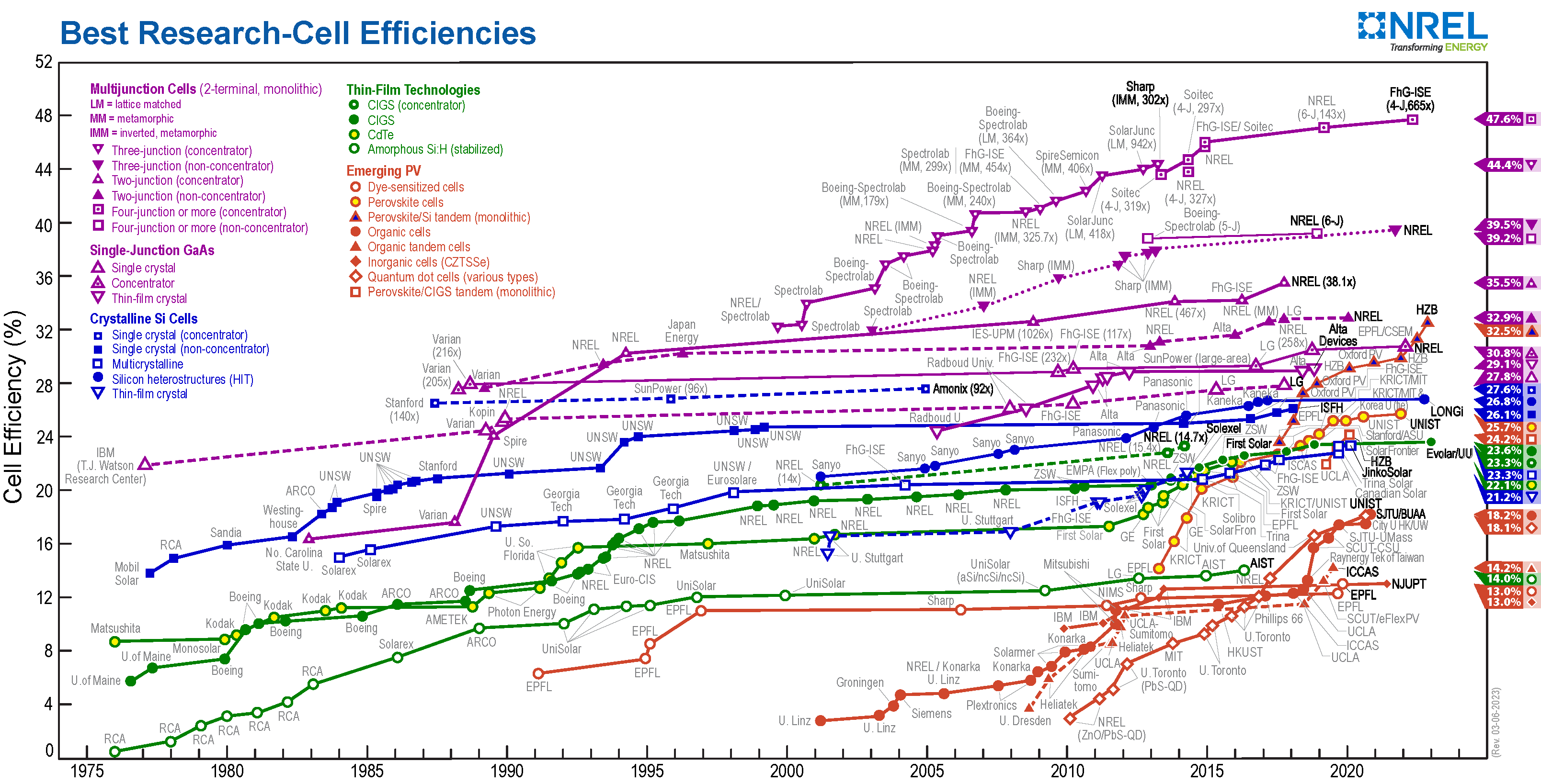
http://upload.wikimedia.org/wikipedia/commons/3/35/Best_Research-Cell_Efficiencies.png
Maximal solar cell efficiency - 44.0% with multiple-junction concentrated photovoltaics.

13
http://ffden-2.phys.uaf.edu/631fall2008_web.dir/wallace_webpage/8_Sun.html
- radiation, which causes the release of electrons in a semiconductor can not be arbitrary,
photons incident radiation must have the necessary energy
- size of required energy depends on the used semiconductor. For silicon is required
energy 1.1 eV, corresponding to a wavelength of 1100 nm
Usable radiation spectrum for Si cells
h
≅ 6,626 . 10
-34
J.s (Planck constant)
- for generation of the power is therefore used only photons with a shorter wavelength,
i.e. with larger energy

14
Series-parallel connection of photovoltaic cells
- crystalline solar cells usually have low power (appr. 1 – 2,5 W in dependency of the size
and material). Also, the voltage reaches a very low value, typically about 0,5 to 0,6 V.
- for practical use of the energy from PV cells, it is necessary to join them into modules and
strings.
- individual cells are connected in series (to increase voltage) and parallel (to increase
current)
- note: usually are used solar panels with power 160 to 240 Wp (output DC voltage about
40 V and the current about 5 A)

15
In most nowadays manufactured panel, individual cells are linked
in series
.
- in this connection, the output voltage is the sum of the voltages of cells, and the current
is as large as the current generated by the weakest cell in the series.
- therefore it is clear that if there is shading of one or more cells (e.g. fallen leaves), the
total generated current in the cell can be decreased down to zero.
Series connection of photovoltaic cells
http://www.solartechnika.sk/solartechnika-32011/pracuje-vase-fotovoltaicka-elektrarna-jak-by-mela.html
- these situations can be prevented by the
bridge (bypass) diode
. In case of shading of
the cell, the current generated in no-shaded cells will flow by bypass diode.

16
- the same solar cells can be connected in parallel, so the output currents are summed
and the output voltage is equal to the output voltage of a single cell.
- however, the problem occurs when there are a large differences between output voltage
of individual cells, when the balancing currents can flow between individual cells
- in case of the shading of cells arranged in parallel, the diodes are also applying, because
in this case the shaded cell acts as a load.
[Hudák, J.: Diplomová práca. 2012. TU v Košiciach]
Parallel connection of photovoltaic cells
http://www.pvpowerway.com/en/knowledge/modules.html
Defective cells in panels
(thermometric measurements)

17
Bypass diodes

18
Currently, the
silicon
is the most used materials for the production of photovoltaic cells. It is used
in several forms, depending on the technology used in production. They are the following forms:
- monocrystalline silicon,
- polycrystalline silicon,
- amorphous silicon (thin film panels).
Materials for the production of PV cells
http://www.solarenvi.sk/s11article10.html
Panels from crystalline silicon
- crystalline silicon cells are formed by cutting of silicon ingots created in a blast furnace at
temperatures of 1500 °C,
- silicon ingot
is a cylinder made of monocrystalline or (or multicrystalline) silicon weighing
about 100 kg, diameter of about 14 cm and a length of over 80 cm,
- conventional crystalline cells have a thickness of about 0,3 mm.
Silicon ingot is cut into thin plates
http://www.solarna-technika.sk/component/content/article/48
For the production of PV cells are also other elements or compounds used. For example: gallium
arsenide, cadmium telluride, cadmium sulphide and finally rapidly expanding organic compounds.

19
Monocrystalline and polycrystalline silicon cell
Monocrystalline silicon panels –
they
are expensive, but have the best effect.
Disadvantage – they are most effective when the sun shines on them straight - in diffuse
radiation efficiency is reduced.
Polycrystalline silicon panels -
they are cheaper, slightly lower efficiency, are much more
sensitive to diffuse the light - the light need not shine directly.
Amorphous panel in good weather and in the
the rain
Amorphous panel
Note: Amorphous silicon panels are
changing colors, the color depends
on the weather and the angle of
view.
Amorphous panels
- amorphous modules are produced in a vacuum chamber at about 200 ° C, where steam is
applied a layer of amorphous silicon on glass, plastic or metal foil
- amorphous silicon is applied in a layer of 0,001 mm (thin film technology).
- production of amorphous modules is therefore cheaper and less material and energy consuming
compared to crystalline technology
- they are less effective, they are the cheapest, least sensitive to the direction of the incident light

20
Comparison of material and energy expenses for production of thin film (left) and crystalline
(right) cells

21
The production process of of photovoltaic cells and modules from the
crystalline silicon
1) Silicon ingot
is the starting material.
It is cylinder from monocrystalline or (or multi-
crystalline) silicon weighing about 100 kg, diameter
about 14 cm and a length of over 80 cm. Silicon
with boron (P-type semiconductor) must meet very
strict criteria (1 boron atom to around 5 million
silicon atoms)
2) cutting the ingot to the plates
with thickness of about 0,3 mm. These plates are the
foundation for future PV cells. By cutting the ingot it is obtained appr. 750 plates with total
weight of about 40 kg. Residues ingot are returning to melt and re-processing.
Silicon ingot (1) is cut into thin plates (2).
http://www.cez.cz/edee/content/microsites/solarni/k41.htm
http://www.1sg.sk/www/data/as/projekty/2006_2007/diamonds/zdroje_energie/webd/solarne.htm

22
3) the etching of plates
- removes damage the surface when cutting. The result is a
textured surface. This surface is creating by miniature silicon pyramids, decreased reflection
of the light. This operation significantly increases the effectiveness of future photocell.
By etching a textured surface is created on the surface of the thin plates (1). A large-scale transition
PN (2) is then formed in the plates.
4) diffusing phosphorus (thus creating wafer-thin layer of N-type semiconductor).
Replacing
one tetravalent silicon atom (4 valence electrons) pentavalent phosphorus atom. With its
incorporation in the crystal lattice its four valence electrons participate in covalent bond and
the fifth electron, which has a covalent bond can not attend, remain poorly bonded to the
phosphorus atom, and even at a relatively low temperature breaks away from him and
becomes a free electron - therefore is the excess of free electrons in silicon polluted by
phosphorus. Thickness of this N layer is about 500 nm, i.e. 0.0005 mm. In this operation
occurs just below the surface silicon plate transition PN which is the basis of the cell
functionality. The original circular plates is cropped to square with rounded corners.
http://www.cez.cz/edee/content/microsites/solarni/k41.htm
http://www.1sg.sk/www/data/as/projekty/2006_2007/diamonds/zdroje_energie/webd/solarne.htm

23
5)
After removing of the phosphorus-silicate glass produced during diffusion surface is
covered with
antireflective layer
. An anti-reflective layer of insulating silicon nitride or
titanium dioxide (SiN
x
alebo TiO
2
) is responsible for reducing surface reflectivity, like texturing
etching. It also protects the surface against mechanical damage. An anti-reflective layer has
a thickness of about 80 nm and causes bluish coloration of PV surface.
http://www.cez.cz/edee/content/microsites/solarni/k41.htm
http://www.1sg.sk/www/data/as/projekty/2006_2007/diamonds/zdroje_energie/webd/solarne.htm
6) Conductive contacts
for the offtake of electricity from the PV cell is made by screen
printing method. On the bottom surface (non-illuminated) the dense grid bus surface is
formed (contacts). On the illuminated part of the surface is in the form of thin conductive
strips. Contacts are smelted across the anti-reflective layer (in high temperatures) to the
silicon material.
Surface of plate covered with anti-reflection layer has a blue tint (1).
Contacts applied by screen printing are smelted in an annealing furnace (2).

24
7) Measurement and grading
is the final stage of
production.
- this operation passes through each cell, because the cells
connected to photovoltaic panels must have
approximately the same properties.
- during the measurement, the cell is irradiated with a
intensity of 1000 W/m
2
(corresponded to sunlight)
- basic parameter for grading is the current generated at
the cell voltage appr. 0.45 V. It means, the cells are
assorted according to the current corresponded to
maximum power point
I
mp
.
http://www.cez.cz/edee/content/microsites/solarni/k41.htm
http://www.1sg.sk/www/data/as/projekty/2006_2007/diamonds/zdroje_energie/webd/solarne.htm
8)
The solar cells from the crystalline silicon have an operating voltage around 0,5 V and a
current density of several tens of mA/cm
2
(≈35 mA/cm
2
).
Photovoltaic panel
is created by serial and parallel connections according to the required
photovoltaic voltage and current. The panel is covered with a translucent plate and airtight
closed to protect against external influences.
The finished cells are measured (1)
and photovoltaic panels are
compiled from them (2).

25
Mechanical construction of PV cells
To achieve the high lifetime of the cells, they must protected against the destructive effects of
the environment.
- solar cells are usually inserted into the ethylene-vinyl acetate (EVA) foil
- the front side is also protected by a highly translucent, specially tempered glass due to
protection of the cell against wind, rain, hailstorm and other weather conditions.
- back side is closed by the multilayer, a highly solid plastic foil or by the second glass plate
and the space between the panes is sealed
- most of the modules for increased stability and better handling has a metal frame, usually
made of aluminum
Mechanical construction of a solar
module with frame:
1. aluminum frame,
2. seal
3. tempered glass,
4. EVA foil
5. PV cell,
6. waterproof plastic foil
http://www.oze.stuba.sk/oze/slnecna-energia/
