1 4
2 2
3 4
4 4
5 2
5 8
6 8
7 4
7 8
Selecting an
Architecture
by Walter Banks
A
Embedded Controller Prototype
by Randy Heisch
Add an I/O Coprocessor to Your Embedded PC
by Bill Houghton
Embedding the ARM7500
Part 1: The Chip and Development Board
by Art Sobel
Four Bits Unleashed
by Brad Stewart
A Universal IR Remote-Control Receiver
by Daniel
Michael Miller
q
Standards for Electromagnetic Compliance Testing
Part 4: Testing Houses
Toe
q
From the Bench
Infrared Remotes are Everywhere...
If You Can Find ‘Em
Bachiochi
q
Silicon Update
Modem
Vu
Tom Can
Task Manager
Ken Davidson
Let’s Do Lunch
I
Reader
Letters to the Editor
New Product News
edited by Harv Weiner
I
1
Excerpts from
the Circuit Cellar BBS
conducted by
Ken Davidson
Priority Interrupt
Steve Ciarcia
Processing-A
Matter of Definition
Advertiser Index
Circuit Cellar INK@
Issue 92 May 1997
OFF THE MAP
DON’T FORGET E-MAIL
I have a couple comments about “The Global
I know the $500 Web browser is attractive to many
tioning System” by Do-While Jones
77 and 78).
manufacturers since they see a huge, currently untapped
All the GPS receivers I’ve encountered display their
market. But, I’d propose they also think about a $50
position in WGS-84 or else give the user a choice of
mail interface with a built-in
modem,
display datum. A practical problem is that most U.S.
based
x lo-line (or even smaller) LCD, and
land maps, including such software as Precision
built-in keyboard, maybe with a parallel port or an Access.-
ping (Chicago Map, Inc.) use the North American Datum
bus port to interface to a printer or desktop system.
of 1927 (NAD-27). Depending on where in the country
E-mail used to be the most used ‘Net application. I
you are, this can give quite a bit of error in transferring
don’t know if that’s still true, but I think many people
your GPS position to a map.
could be enticed into Internet computing through
a
There are two DOS shareware programs that can
device, especially since E-mail is primarily text based.
help. DATUM converts one datum to another and
includes 99 different systems the author located in
David Bley
worldwide use. (It includes both WGS-84 and NAD-27.)
The other program, GEOD, calculates surface distance
between a pair of Earth coordinates.
BACK IN THE FAMILY
Ron
A CALL TO ALARMS
Recently, my family’s house was
The thieves kicked in the front door and stole two
My dirty little secret is that I read my cousin Chris
Arndt’s article
The X-10 Radio-Control
System,” INK 80) in a borrowed copy of INK! I liked the
whole magazine so much, I subscribed on the spot!
I used to read Steve’s columns years ago when he
wrote for BYTE. He stopped the columns, and I dropped
BYTE. Somehow, I never got caught up again-till now.
complete AMD computer systems, two televisions, a
L. M.
VCR, a halogen desk lamp, and my daughter’s backpack.
Although they took the computers-speakers, mice,
surge protectors, and all-they left my checkbook
behind. Interestingly enough, they made off with a 6”
silicon IC wafer and my copy of Circuit Cellar INK.
Obviously, they were real connoisseurs!
This type of crime is on the rise. Computers are
especially tempting targets because they can be
sembled, making them virtually impossible to trace.
Contacting Circuit Cellar
We at Circuit Cellar
communication between
our readers and our staff, so we have made every effort to make
contacting us easy. We prefer electronic communications, but
feel free to use any of the following:
As fellow computer users, don’t forget to take steps to
Mail: Letters to the Editor may be sent to: Editor, Circuit Cellar INK,
deter criminals from selecting your home. Protect your
4 Park St., Vernon, CT 06066.
possessions. Invest in an alarm system. Make sure your
Phone: Direct all subscription inquiries to (800) 269-6301.
doors and locks are secure.
Contact our editorial off ices at (860) 875-2199.
Consider marking your valuables, especially the
Fax: All faxes may be sent to (860)
expensive electronics. A permanently marked item is
BBS: All of our editors and regular authors frequent the Circuit
worthless on the black market. Keep an accurate
Cellar BBS and are available to answer questions. Call
inventory of your possessions (i.e., the make, model,
(860) 871-1988 with your modem
bps,
purchase data and price, and serial number).
Internet: Letters to the editor may be sent to
And, don’t make the big mistake I did-always back
corn. Send new subscription orders, renewals, and
up your computer data. As it slowly dawns on me how
dress changes to
Be sure to
much work I lost, I wish I’d invested a few hundred
include your complete mailing address and return E-mail
dollars on data insurance.
address in all correspondence. Author E-mail addresses
(when available) may be found at the end of each article.
Chip Freitag
For more information, send E-mail to
WWW: Point your browser to
6
Issue 82 May
1997
Circuit Cellar INK@
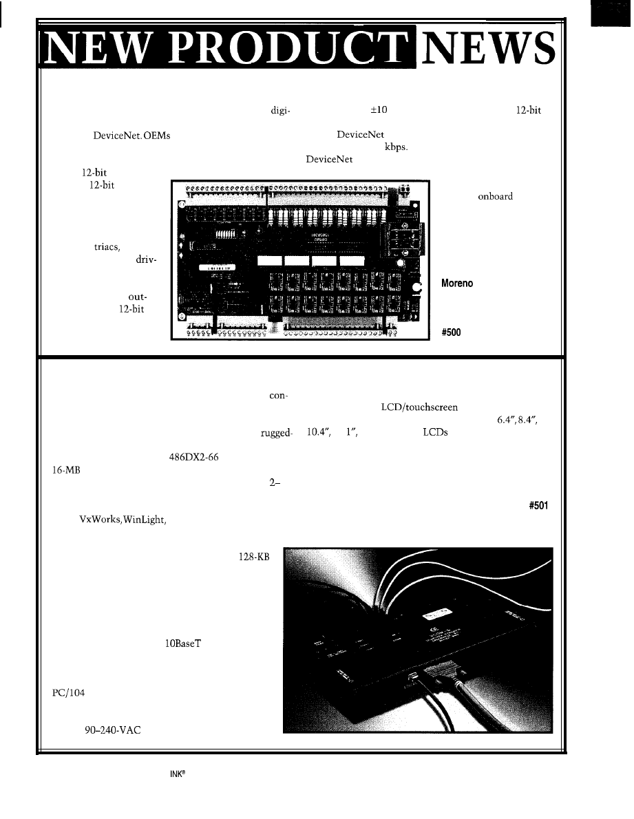
I/O CONTROL FOR DEVICENET
Edited by Harv Weiner
The DN502 provides a wide range of analog and
O-5 V, O-10 V,
V, or a current loop. The four
tal I/O capability for use with distributed I/O systems
analog outputs are configured for 0-10-V operation.
using the
may specify the exact I/O
The
interface may be configured to be fully
mix for custom applications.
isolated up to 500
A second option permits the
The DN502 contains 16 digital inputs and outputs, 8
power to provide power to the controller. The
analog
inputs, and
MAC ID and operating
4 analog
outputs.
speed may be configured
The digital inputs can be
from an
switch
120 VAC or 24 VAC/DC
or under software.
and the outputs may be
The fully configured
specified with relays,
DN502 sells for $710.
120-VAC
or
24-VDC solid-state
DIP Industrial Products
ers. Status indicators
P.O. Box 9550
show the state of all
Valley, CA 92552
digital inputs and
(909) 924-l 730
puts. The eight
Fax: (909) 924-3359
analog inputs may be
software configurable for
EMBEDDED COMMUNICATIONS CONTROLLER
The VCOM-6 is an embedded communications
70°C with no fan required. The VCOM-6 is available
troller that offers full European, U.S., and Canadian
with an optional
kit that can be
agency approvals. The unit is designed for OEM and
mounted remotely. Display choices include
end-user machine-control applications requiring
12. and 13.8” TFT
with guided acoustic
ness, a variety of I/O, and small size.
wave, IR, and resistive touchscreens.
The VCOM-6 features a
SBC with up to
The VCOM-6 sells for $1425.
DRAM. Since operating from solid-state memory
greatly improves system reliability, the unit offers
Computer Dynamics
32 MB of flash memory configurable as the boot drive.
7640 Pelham Rd.
l
Greenville, SC 29615
It’s well-suited for embedded operating systems such as
(864) 627-8800
l
Fax: (864) 675-0106
QNX,
and ROM-DOS. Pro-
gram changes can be made remotely via serial port
using a software utility program that enables firm-
ware to be downloaded to flash memory. A
battery-backed SRAM is also included for nonvola-
tile memory.
The VCOM-6 video controller directly drives
flat-panel displays (e.g., CRTs) and features Low
Voltage Differential Signaling (LVDS) to lower EM1
and RFI. All communications ports (six RS-232
ports capable of 115 kbps,
Ethernet inter-
face, and video connector) are mounted in the metal
housing for easy access. An optional hard/floppy
disk-drive interface card can be added via the unit’s
connector.
The complete system measures 14” x 9” x 2” and
includes a 65-W autosensing power supply that
accepts
input. It operates from 0” to
8
Issue
92 May 1997
Circuit Cellar
SERIAL RAM MODULE
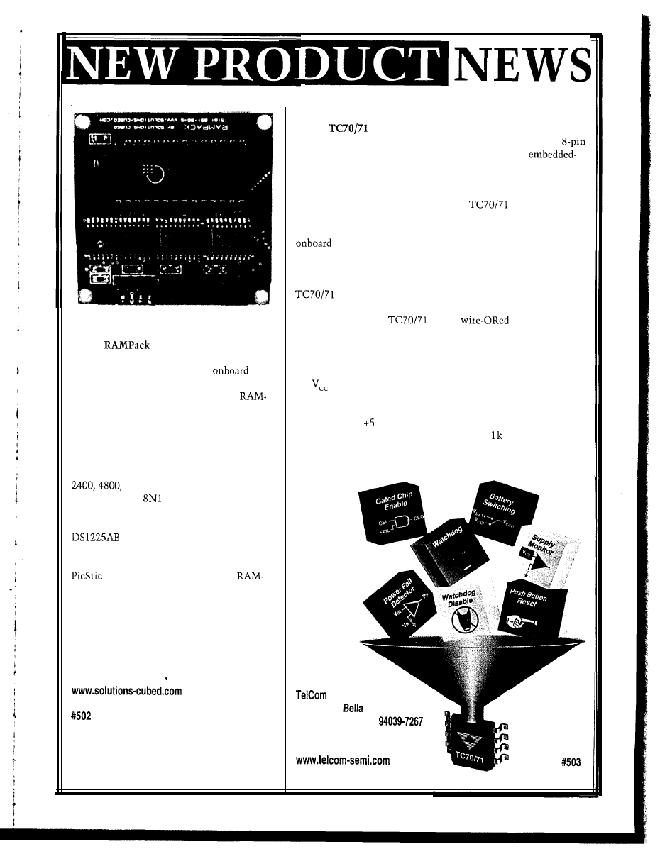
The
module provides low-cost
serial storage of data into 8 KB of RAM. The
module employs buffers and an
microcontroller to allow addressable access
to the RAM using only two I/O lines.
Pack can store data from data loggers or ex-
tend variable space in microcontrollers. It
can also serve as a serial data buffer.
An automatic baud-rate detection scheme
enables a variety of baud rates to be selected
without hardware jumpers. Rates of 1200,
and 9600 bps are supported using
a specific serial
communications proto-
col. The SRAM provided with the system is
socketed so that it can be replaced with a
NVRAM, if desired. NVRAM
retains data after power is lost or removed.
The 2” x 2” board is perfect for use with
or BASIC Stamp designs. The
Pack sells for $24.95. NVRAM is sold sepa-
rately.
Solutions Cubed
3029 Esplanade, Ste. F
Chico, CA 95973
(916) 891-8045
Fax: (916) 891-1643
SYSTEM SUPERVISOR CHIP
The
is a fully-integrated power-supply monitor, reset
generator, watchdog timer, and battery-backup circuit in an
package. The chips are ideal for applications such as
control and mission-critical microprocessor-based systems. Other
typical applications include test equipment, instrumentation, and
set-top boxes.
When power is initially applied, the
holds the proces-
sor in its reset state for a minimum of 500 ms to ensure stable
system startup. After startup, processor sanity is monitored by the
watchdog circuit. The processor must provide periodic
high-to-low level transitions to the chip to verify proper execution.
Should the processor fail to supply this signal within the specified
timeout period, an out-of-control processor is indicated and the
issues a momentary processor reset. The TC70 also fea-
tures a watchdog disable pin to facilitate system test and debug.
The output of the
can be
to a push-button
switch (or electronic signal) to reset the processor. When connected
to a push-button switch, the chip provides contact debounce. The
chip’s integrated battery-backup circuit converts CMOS RAM into
nonvolatile memory by first write-protecting and then switching
the
line of the RAM over to an external battery. The TC71
incorporates an additional 1.3-V threshold detector for power-fail
warning, low-battery detection, or monitoring power-supply volt-
ages other than V.
Pricing for the TC70 or TC71 is $1.57 in
quantities.
Semiconductor, Inc.
1300 Terra
Ave.
Mountain View, CA
(415) 968-9241
Fax: (415) 967-l 590
Circuit Cellar INK@
Issue 82
May
1997
9
SERIAL-INTERFACE LCD
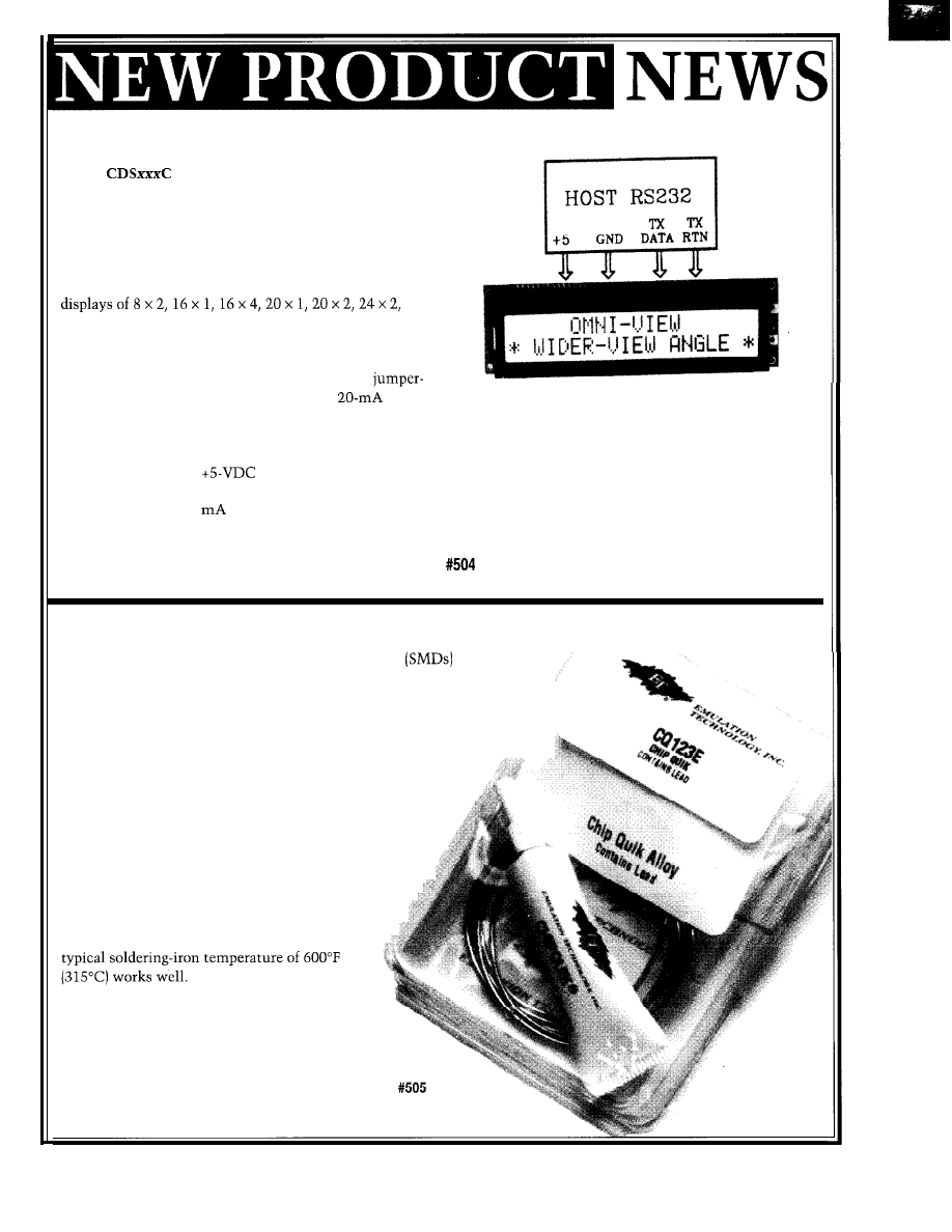
The
line of character-based LCD modules
features a serial RS-232 interface to a host processor.
The modules can be used for OEM applications where
only serial I/O ports are available or where extended
cable lengths for host-to-display data communications
are required.
The full line of serial modules includes character
40 x 2, and 40 x 4 (characters x lines). Versions are avail-
able with supertwist fluid for wide viewing angle, ex-
tended temperature range, and LED or EL backlighting.
The modules accept serial data at one of four
selectable baud rates at RS-232, RS-422, or
cur-
rent loop levels. Data word arrangements and parity are
also selectable. Display instructions are a serial version
of the industry-standard HD44780 LCD controller. Most
modules require only
input and a single mating
connector or cable of 9-l 1 pins. Power consumption is
typically less than 35
excluding backlighting, if
required.
Prices in 100 units for the complete assembly start at
$35 for a reflective supertwist 16 x 2 character display
and go up to $89 for an LED backlit, supertwist 40 x 4
character display.
Apollo Display Technologies, Inc.
194-22 Morris Ave.
Holtsville, NY 11742
(516) 654-l 143
Fax: (516) 654-l 496
SMD REMOVAL KIT
A method for removing Surface Mounted Devices
with-
out damage to circuit boards or components is available from Emu-
lation Technology. The Chip Quik SMD Removal Kit, a specially
formulated alloy in wire form, is designed to melt at the low
temperature of 136°F (58°C).
The removal process is surprisingly easy. A special liquid
flux is applied to all leads of the SMD to be removed. A
soldering iron is then used to melt the Chip Quik alloy
uniformly on all leads of the SMD. The iron keeps the
alloy in a molten state long enough to dissolve into
the existing solder. The resultant molten tempera-
ture of the two alloys causes complete reflow at a
temperature less than 220°F (93°C). While in this
molten state, the SMD can easily be removed
with a vacuum pen. The iron’s temperature
determines the speed of the process. A
Emulation Technology, Inc.
2344 Walsh Ave., Bldg. F
Santa Clara, CA 95051-1301
(408) 982-0660
Fax: (408) 982-0664
Circuit Cellar INK@
Issue 82
May 1997
11
NEWS
MACRO CROSS-ASSEMBLER
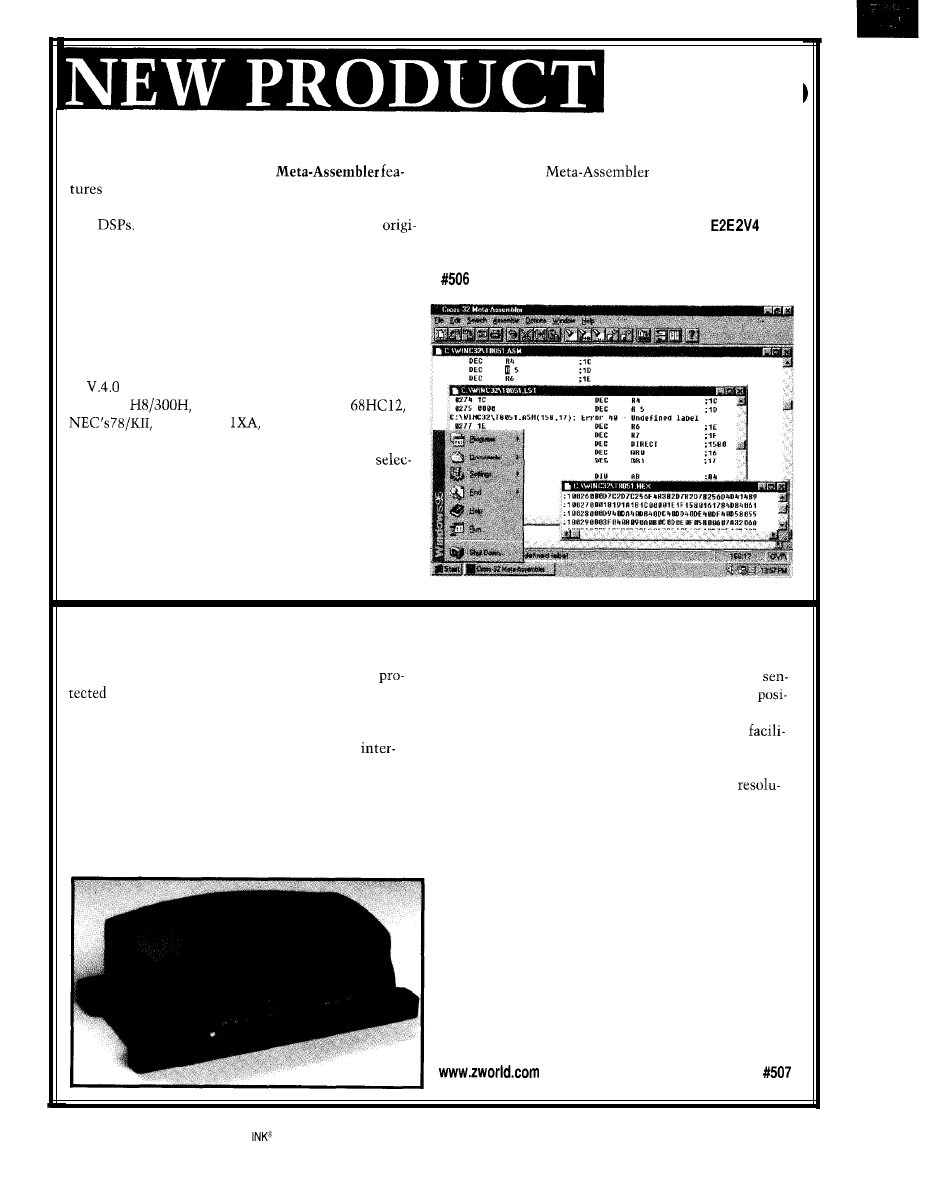
The Windows-based Cross-32
The Cross-32
sells for $199.
table-driven macro cross-assemblers that compile
assembler programs for over 50 processors, controllers,
Universal Cross-Assemblers
and
The tables use the chip manufacturer’s
9 Westminster Dr.
l
Quispamsis, NB
l
Canada
nal assembly-language mnemonics. Full instructions are
(506) 849-8952
l
Fax: (506) 847-0681
included so you can create new tables for other chips.
Cross-32 reads an assembly-language source file and a
corresponding assembler instruction table and then
writes list, error, and absolute hexadecimal machine
files in binary, Intel, or Motorola formats. The hexadeci-
mal file can then be downloaded to most EPROM pro-
grammers, EPROM emulators, and in-circuit emulators.
includes support for many new chips, such as
Hitachi’s
Intel’s 80251, Motorola’s
Philip’s 805
and Zilog’s 2380, among
others. The text editors handle up to a billion lines of
code with adjustable tab sizes and Windows font
tion. A literal text replacement directive (RPTXT) lets
you replace almost any register or variable with any text
string, making code easier to read and the assembler
more versatile. Support for IEEE floating-point number
definitions (DFF) is provided, along with the option of
making the assembler case sensitive (CASE).
C-PROGRAMMABLE CONTROLLER
The Z-World PK2300 is a versatile controller that
includes KS-232 and RS-485 serial communication ports,
contains user-configurable I/O providing up to 16
power supervision, a real-time clock, and a resistive
digital inputs and 8 high-current outputs. Initially,
sor-measurement input for capturing temperature,
the 19 I/O lines are set as 11 inputs and 8 outputs, but 5
tion, and potentiometer values. Flash memory enables
of the outputs and 6 of the inputs are jumper selectable.
nonvolatile storage of program code and data and
Possible configurations include level-sensitive
tates remote programming. Easy-to-use software drivers
rupts and protected inputs, an analog-resistive input,
are included for all I/O, including PWM for seven of the
and an RS-485 port. Screw terminals facilitate quick
eight high-current drivers. PWM frequency and
wiring, and the rugged enclosure easily mounts to a flat
tion are adjustable under software control.
surface or any of the three DIN rail sizes.
The PK2300 is programmed using Z-World’s Dynamic
The PK2300 features high-current outputs that can
C, a version of the industry-standard C programming
drive inductive loads (e.g., solenoids and relays). It also
language optimized for real-time control. Dynamic C is a
software development system that’s an integrated editor,
compiler, and interactive debugger. The compiler, run-
ning on a host PC, compiles directly into the 128 KB of
flash memory of the PK2300 for in-target software devel-
opment. This feature eliminates the need for expensive
test equipment (e.g., ROM or in-circuit emulators).
Pricing in single quantities is $179.
Z-World
1724 Picasso Ave.
l
Davis, CA 95616
(916) 757-3737
l
Fax: (916) 753-5141
12
Issue 82 May
1997
Circuit Cellar
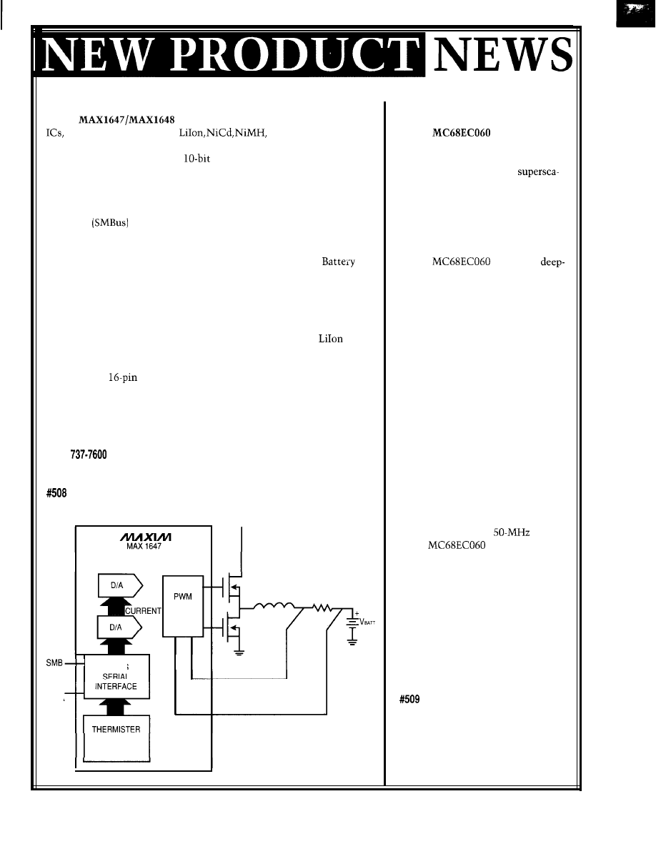
CHEMISTRY-INDEPENDENT BATTERY CHARGER
The
are chemistry-independent battery-charger
each capable of charging
and other battery
types. The chargers provide 1 l-bit resolution for control of the charging
current (4, 2, or 1 A max.) and
resolution for control of the ap-
plied compliance voltage (18 V max.).
The MAX1648 delivers charging voltage and current to the battery in
proportion to control voltages applied to its input pins. The MAX1647
sets these parameters via its interface to the two-wire System Manage-
ment Bus
by Intel. This bus enables the MAX1647 to set the
charging voltage and current and provide thermal status information to
the external system.
The MAX1647 is compliant with the Duracell/Intel Smart
Charger specification as a Level 2 charger. In addition, it generates inter-
rupts that signal the host when power is applied to the charger or when a
battery is installed or removed. Other status bits enable the host to check
whether the charger has enough input voltage and whether the battery
current and voltage are properly regulated. This capability allows the
host to determine, without interrogating the battery, when a
bat-
tery is fully charged.
The MAX1647 is available in a 20-pin SSOP, and the MAX1648 is
available in a
DIP. Prices start at $4.75 for the MAX1647 and
$4.25 for the MAX1648 in quantity.
Maxim Integrated Products
120 San Gabriel Dr.
Sunnyvale, CA 94086
(408)
Fax: (408) 737-7194
DC INPUT
VOLTAGE
CLK
SMBUS
SMB
DATA
COMPARATORS
AND AC DETECT
SUPERSCALAR
MICROPROCESSOR
The
is an implemen-
tation of an MC68060 optimized for
embedded applications. It provides
the highest level of 680x0
lar integer performance of 102 MIPS
at 66 MHz. Its high performance,
low power consumption, and eco-
nomical pricing make it an excellent
solution for cost-sensitive advanced
applications in embedded control.
The
employs a
pipeline, dual-issue superscalar ex-
ecution, a branch cache, and 8 KB
each of on-chip instruction and data
caches. Its architecture permits si-
multaneous execution of one branch
and two integer instructions during
each clock cycle. The microproces-
sor automatically minimizes power
dissipation via fully static design,
dynamic power management, and
low-voltage operation. It also auto-
matically powers down internal
functional blocks that aren’t needed
on a clock-by-clock basis. Power
consumption can be controlled from
the operating system.
The chip is available in a 206-lead
ceramic Pin Grid Array (PGA) and
operates off of a single 3.3-V power
supply. It is also 5-V input tolerant.
The list price for the
version
of the
is $75 in quan-
tity. The 66-MHz version costs $180
in quantity.
Motorola
Communications and Advanced
Consumer Technologies Group
6501 William Cannon Dr. W
Austin, TX 787358598
(512) 891-2134
Fax: (512) 891-4465
Circuit Cellar INK@
Issue 82
May 1997
13
FEATURES
Selecting an
Architecture
A
Embedded Controller
Prototype
Add an Coprocessor to
Your Embedded PC
Embedding
the ARM7500
Four Bits Unleashed
A Universal IR
Remote-Control Receiver
Walter Banks
Selecting an
Architecture
ost
embedded
crocomputers
from a
chip processor of the
1970s. And, those were based on the
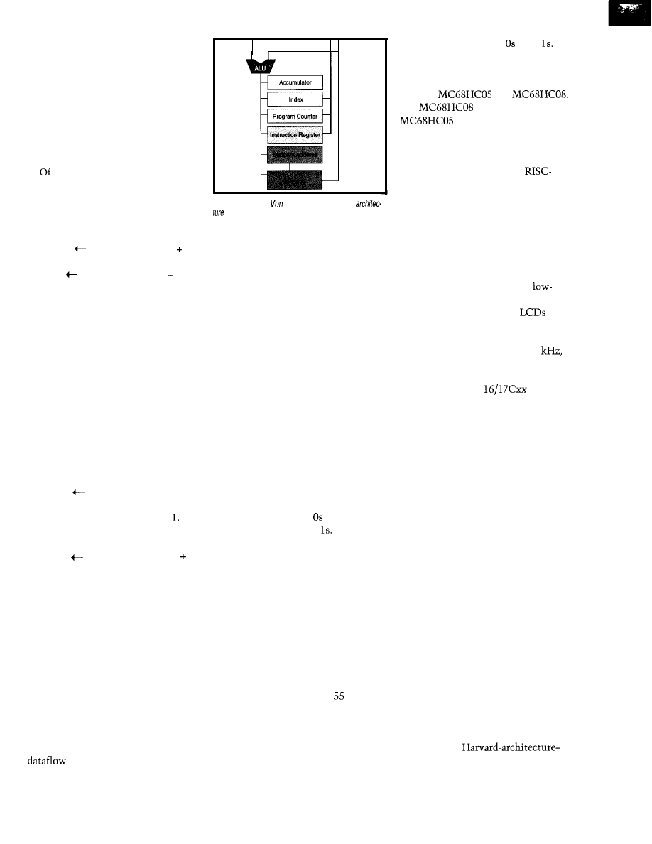
minicomputers of a decade earlier.
The dominant processor architecture
was the classical Von Neumann com-
puter with a uniform address space
containing memory that could be used
for either program or data storage.
Figure 1 shows the Von Neumann
architecture.
The systems’ designs were simple
and easy to program. Most of these
computers used a small number of
general-purpose registers for arithmetic
calculations.
Designers found that an applica-
tion’s execution speed depended on the
rate that data could be passed through
the registers performing calculations.
By increasing the number of
purpose registers or by making access
to the data registers quicker, substan-
tial improvements in performance
could be achieved while still using the
same basic logic-operation speed.
By overlapping access to the instruc-
tion with data accesses, a style of pro-
cessor with separate instruction and
data spaces was developed. This style
was further optimized by tailoring the
size of the instruction and data space
to the intended application’s require-
ments.
14
Issue 82 May
1997
Circuit Cellar INK@
Extending the width of the instruc-
tion word (i.e., increasing its parallel-
ism) meant fewer instruction fetches
were needed to execute a given task,
resulting in even better system perfor-
mance. It became reasonable that data
paths were 4 or 8 bits and instruction
paths were 12, 16, or more bits.
CARRY IN SUBTRACTS
all computer instructions, sub-
tract is the one instruction that’s least
consistently implemented. Here’s a
nonexhaustive list of different imple-
mentations:
register register + *memory
1
register tregister + (*memory +
1)
register register + *memory carry
register t register + *memory + *carry
The first two implementations may
seem identical, and certainly they
generate correct results. But, when
zero is the value in memory, the carry
bit is set in the first case and cleared in
the second case.
In many microprocessors, the com-
pare instruction (if it exists) is based
on the subtract, so interpreting results
can be difficult.
Let’s looks at an example where
both register and memory are initially
both equal to 0:
register register + *memory + 1
results in register = 0 and carry = But,
when:
register register + (*memory
1)
then register = 0 and carry = 0.
The resulting carry may be different
depending on the order of execution in
the processor ALU. This can change
how compares are evaluated between
processors with similar architectures.
MEMORY-TO-MEMORY MOVES
On the surface, memory-to-memory
move instructions appear to be a small
savings in the ROM requirements as
well as in one less opcode fetch. This
is certainly true for data initialization.
Another saving from improved
is often overlooked. Many
times, a value has to be read from a
1
Figure I-Classical
Neumann
computer
stores
both program and dafa
information in the
same
address
space.
sensor or port, saved, and used later for
calculations. Avoiding the use of the
accumulator means that code savings
can be substantial, saving and restor-
ing the accumulator as well as the
saved opcode fetch.
OVERFLOW BIT
Of all the condition code bits, the
overflow bit (V bit) is the least under-
stood. Primarily, its role is akin to the
carry bit for signed numbers. A surpris-
ing number of embedded microcom-
puter applications are implemented on
processors lacking an overflow bit.
Signed numbers are represented by
a circular number system whose small-
est number has only the most signifi-
cant bit (MSB) set and the largest has
only the MSB cleared. This system is
unlike unsigned numbers where the
smallest number is all and the larg-
est is represented by all
During implementation, the code to
compare numbers is the same for equal-
ity and nonequality for both signed
and unsigned number systems.
Most microcomputer instruction
sets lacking a V bit can clearly com-
pare unsigned magnitudes, but signed
compares of relative magnitudes can
be a considerable problem. Most tradi-
tional approaches fail in some of the
many possible combinations. (In com-
piler implementations I’ve done, there
are rules for no fewer than special
cases of comparisons.)
The need for the V bit is extremely
application dependent. To implement
a signed compare without a V bit, I
rotate the number system when execut-
ing comparisons so the signed number
system ranges from all to all All
comparisons are then executed with
just the carry and zero bits.
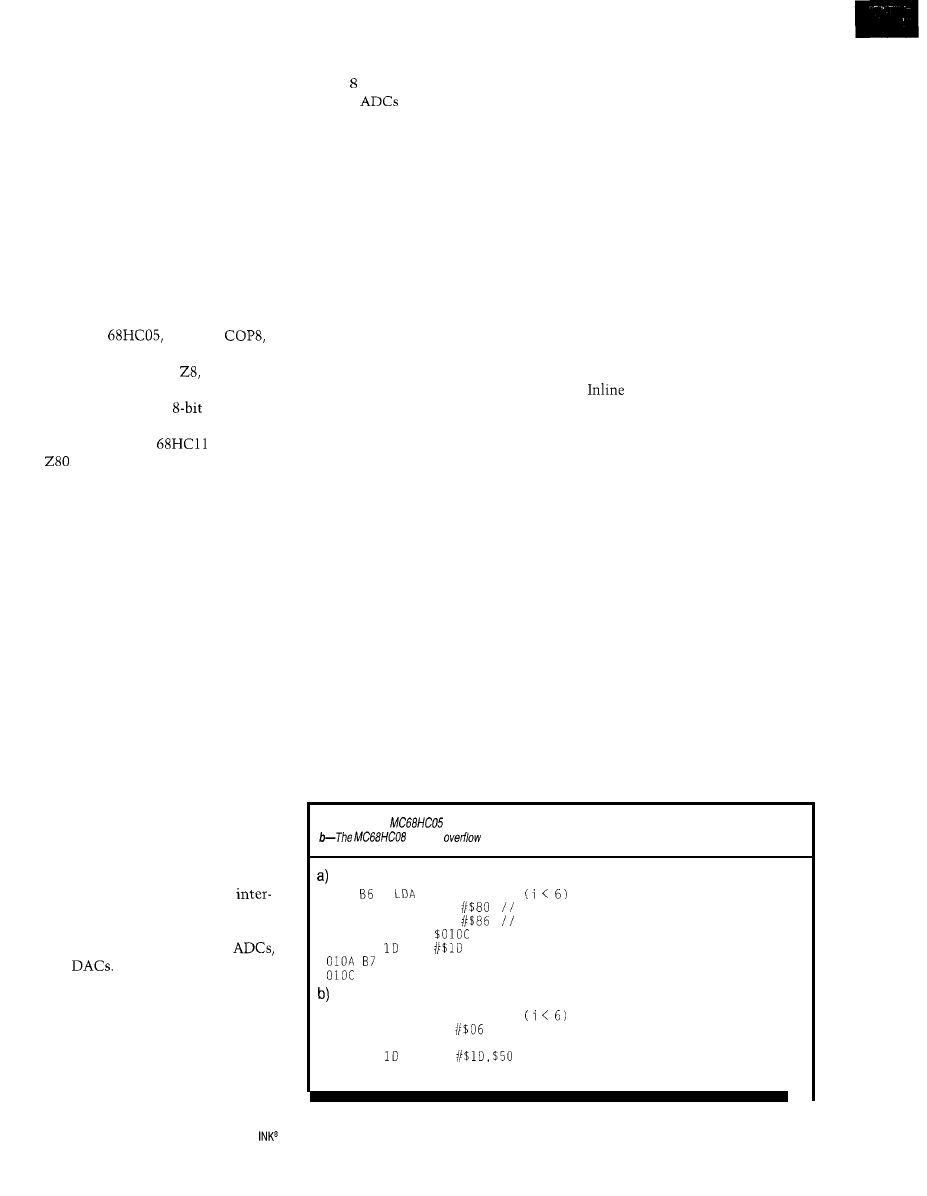
Listing
1
compares the generated
code for
and
The
has a V bit, and the
does not.
RISC IN EMBEDDED SYSTEMS
At least two vendors-Microchip
and Sanyo-have developed
architecture embedded micros that
execute at essentially one instruction
per clock cycle. In both cases, they use
a Harvard architecture (see Figure 2)
with different instruction word and
data sizes.
The Sanyo processor instruction
space is
16
bits, and the data space is
4 bits. This part is targeted to
power, low-speed, high-volume appli-
cations involving time and
(e.g.,
watches and consumer products).
RISC meets the processor’s need for
low power. The clock rate is 32
and the processor rate is 4096 instruc-
tions per second.
Microchip’s PIC
proces-
sors are unique. The instruction paths
are 12, 14, or 16 bits wide, and the data
path is 8 bits.
The RISC aspect of Microchip’s
processor is only one of its advantages.
The instruction set is designed so many
of the traditional load-operate-store
sequences can be executed with the
two-instruction load-operate sequence.
By combining the operate-store pair in
one cycle, the PIC processors can be
impressively fast.
The separate instruction and data
space of both these processors cause
them to share the problems of constant
data found in most Harvard-architec-
ture computers. Constant data arrays
are either not available or very diffi-
cult to reach.
In a similar manner, RAM address-
ing in a Harvard-architecture-based
processor is a compromise of code
representation, size, and address space.
Instruction-set designers solve this
problem by extending the number of
addressing modes or implementing a
RAM memory-management scheme.
Almost all
based processors have a memory-man-
agement scheme available. This isn’t a
Circuit Cellar INK@
Issue 82
May
1997
15
problem, but to achieve efficient code,
care must be taken in locating variables
in RAM.
What about I/O? There are three
common ways of implementing I/O on
embedded computer systems:
l
map the I/O control registers into the
data space on the microcomputer
l
develop a separate I/O address space
serviced with extra I/O instructions
l
add I/O application-specific instruc-
tions
Starting with an informal survey of
Motorola
National
Intel 8051, Microchip PIC series of
processors, and Zilog
I discovered
remarkable similarities between the
offerings from these
processor
families. Although not included in the
list, the Motorola
and Zilog
also have similar I/O resources.
Together, these processor families
have 95% of the market in application
designs and production volume. Al-
though functionally similar, each fam-
ily has implementation quirks that tax
potential portability between platforms.
PORTS
Port support is perhaps the simplest
I/O support for embedded systems, but
initializing the data direction-control
registers complicates it. On some pro-
cessors, initialization requires a 1, and
others, a control bit of 0.
The serial-port I/O support for both
synchronous and asynchronous serial
protocols is available from many ven-
dors. Most serial-port implementations
contain baud-rate generators and, in
some cases, hardware to assist in imple-
menting synchronous serial protocols.
This family of serial I/O support
buses can provide a wide variety of I/O
support facilities ranging from
processor communications to inter-
faces with external serial and parallel
ports, RAM, ROM, EEPROM,
and
Multiprocessor implemen-
tations of sub
$1
microcontrollers are
using this technology for interprocessor
communications.
CONVERSIONS
Embedded microcomputers have
between one and eight analog input
16
Issue
82 May 1997
Circuit Cellar
channels with current resolution be-
tween and 16 bits.
Most
need some general
setup. Typical setups require a refer-
ence source and sometimes resolution
and conversion time parameters. In
looking at application code, I’ve noticed
that this doesn’t change over the course
of code execution in an application.
Very few embedded systems have a
DAC built into them. In some applica-
tions, PWM ports generate an analog
output voltage smoothed with a simple
low-pass filter.
PWM ports are flexible output ports
that can generate levels, sophisticated
pulse trains, and with a simple low-pass
filter, analog outputs. The number of
PWM channels varies from 2 to 16,
with the generated pulse-stream reso-
lution between 6 and 14 bits.
WATCHDOG TIMERS
Embedded systems use watchdog
timers as a check against runaway
execution of code. Their hardware
implementation varies considerably
between different processors.
In general, these timers must be
turned on once, often within the first
few cycles, after being reset. They must
then be reset periodically within the
software. Some can be programmed for
different time-out delays.
The reset sequence can be as simple
as a specialized instruction or as com-
plex as sending a sequence of bytes to
a port. Watchdog timers either reset
the processor or execute an interrupt
on timeout.
HIGH-LEVEL LANGUAGES
High-level languages, the most
common being C, are frequently used
on embedded microcomputers. There
are several standard arguments-devel-
opment ease, maintainability, portabil-
ity-to using high-level languages.
High-level languages let you avoid
the need for alternative sources for the
embedded processors. A well-supported
high-level language can enable applica-
tions to run on several platforms.
Early implementations of C tended
to be based on a mythical model of an
ideal C machine. The elements of this
model were then run on various target
micros either by making library calls
or through macro expansion.
code was, for the most part,
generated by using a subset of the
whole instruction set. The result was a
quick implementation with good port-
ability between various targets. This
approach was useful for prototyping
and applications where execution time
was not too critical, involving low
production volumes.
With the arrival of the PC and the
need for better application performance
and reasonable costs, a new era of
software tools began to appear in the
marketplace.
Good optimizing C compilers are
now available for most common em-
bedded microcomputers. Their code
competes with well-written assembler,
requiring technology that could exhaus-
tively optimize the generated code.
Here’s just how complex the task can
be:
Listing la--The
code compares two signed numbers using the carry bit as an overflow indicator.
uses an
bit for comparing signed numbers.
0 1 0 0 50
$50
if i = 29;
0102 A8 80 EOR
Load I rotate number system
0104 Al 86 CMP
Compare against 6 in new number system
0106 24 04 BCC
0108 A6
LDA
50 STA $50
81
RTS
0100 B6 50
LDA $50
if i = 29;
0102 Al 06
CMP
0104 90 03
BGE $0109
0106 6E
50 MOV
0109 81
RTS
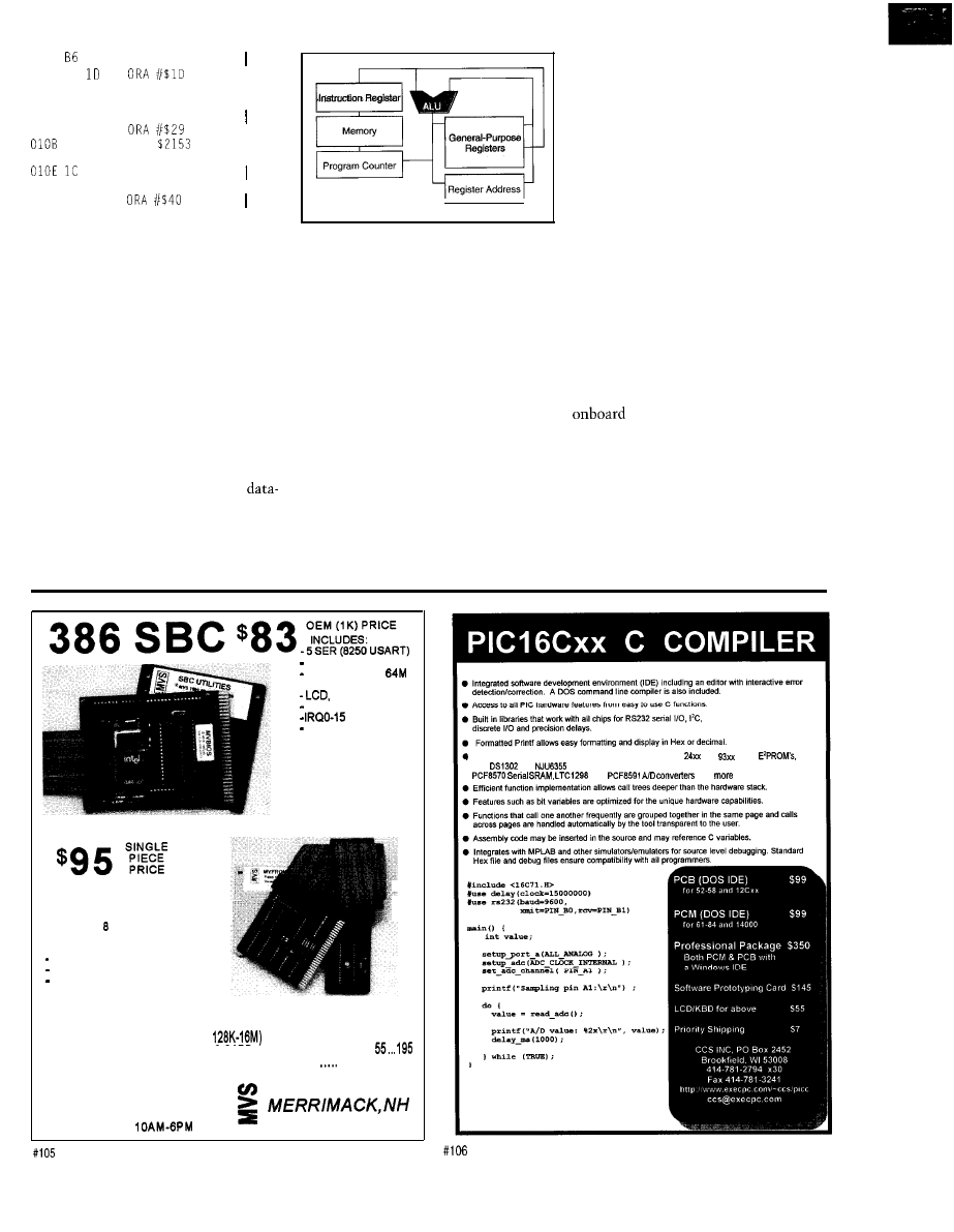
0100
44
LDA $44
i = i
29:
0102 AA
0104 B7 44
STA $44
0106 C6 21 53 LDA $2153 j = j
41;
0109 AA 29
C7 21 53 STA
44
BSET 6,844 i = i
64;
0110 AA 40
j = j
64:
0112 C7 21 53 STA $2153
In each source line, syntactically iden-
tical code generates different results.
The generated code varies between
two and eight bytes, depending on data
location, known data, and previous
execution history in the application.
WHICH MICRO?
There are many available micro-
computers on the market for embed-
ded applications. At last count, about
50 varieties were competing for engi-
neers’ embedded designs. Just say the
word, and there will be a flood of
books and helpful field-application
engineers at your door.
Think about the important issues in
the application. To name a few, the
Figure
P-Harvard architecture has separate code and
data memory spaces.
underlying technology must address
issues of power consumption, number
of I/O pins, cost, size, and availability.
Timely execution of the application
code and the ability to transfer the
application algorithms to the underly-
ing silicon are also important.
SUPPORT
Embedded applications are com-
plex, usually requiring both a clear
understanding of the application area
and the implementation technology.
Chip-vendor field-application engi-
neers are usually well-equipped to
provide answers to all your questions.
Support also comes from vendor
seminars, conferences, reference mate-
rial, and software-tool vendors. Most
silicon and software-tool vendors have
Web sites supporting their products.
These sources give you clues about the
acceptability of a particular product or
tool for a specific application.
Finally, talk to the people who
develop the tools. These individuals
are usually willing to frankly discuss
the strengths (and weaknesses) of their
product.
TIMES ARE CHANGING
Starting about five years ago, most
silicon vendors competed against each
other with functionally similar prod-
ucts. Single-chip computers had some
RAM, ROM, or EPROM and
perhaps
10
pins of I/O. At least half of
the top-ten selling micros could easily
be substituted with minimum board
redesign and receding an already work-
ing application.
Application designers are now able
to put out layout boards that accept
silicon from more than one vendor.
3 PAR (32 BITS MAX)
32K RAM, EXP
-STANDARD PC BUS
KBD PORT
BATT. BACK. RTC
(8259 X2)
0237 DMA 0253 TMR
-BUILT-IN LED DISP.
-UP TO 8 MEG ROM
-CMOS NVRAM
USE TURBO C,
BASIC, MASM
RUNS DOS AND
WINDOWS
EVAL KIT $295
UNIVERSAL
PROGRAMMER
-DOES
MEG EPROMS
-CMOS, EE, FLASH, NVRAM
-EASIER TO USE THAN MOST
POWERFUL SCRIPT ABILITY
MICROCONT. ADAPTERS
PLCC. MINI-DIP ADAPTERS
-SUPER FAST ALGORITHMS
OTHER PRODUCTS:
8088 SINGLE BOARD COMPUTER . . . . . . . OEM $27 . . . ‘95
PC FLASH/ROM DISKS
16 BIT 16 CHAN ADC-Da
. . . . . . . . . . . . . . . . . . 21 . . . . . 75
C CARD . . . . . . . . . . . . . . . . . . . . .
WATCHDOG (REBOOTS PC ON HANGUP)
27 . . . . . 95
‘EVAL KITS INCLUDE MANUAL
BRACKET AND SOFTWARE.
MVS BOX 850
5
YR LIMITED WARRANTY
FREE SHIPPING
HRS: MON-FRI
EST
a
.
(508) 792 9507
Source code drivers included for LCD modules, keypads,
and
serial
X10,
and
Real Time Clocks, Dallas Touch Memory Devices, DS2223 and
and
and
Circuit
Cellar INK@
Issue 82 May
1997
19
Effective high-level language tools
enable application code to be retargeted
easily between the most popular pro-
cessors.
Maybe I’m venturing too far into
the future, but I’m starting to see ven-
dors of standardized VHDL models
waiting for the day when a large FPGA
implements whole applications.
At the engineering level, local sup-
port is crucial. Getting answers to hard
technical questions ranks as an engi-
neer’s most critical need.
From my experience with both
vendors and customers from various
competing companies, I know that the
single most important issue to getting
a product out to the marketplace is
development support, closely followed
by product availability.
q
Special thanks to Bruno Bratti, who
surveyed the
facilities on the most
popular microcomputer products. His
work served as a foundation for mine.
Walter Banks is president of Byte
Craft Limited, a company specializing
in software tools for embedded micro-
processors. His interests include highly
reliable system design, code-generation
technology, programming-language
development, and formal code-verifi-
cation tools. You may reach him at
8051
Intel Corp.
5000 W. Chandler Blvd.
Chandler, AZ 85226-3699
(602) 554-8080
Fax: (602) 554-7436
Microchip Technology, Inc.
2355 W. Chandler Blvd.
Chandler, AZ 85224-6199
(602) 786-7200
Fax: (602) 786-7277
www.microchip.com
Motorola
MCU Information Line
P.O. Box 13026
Austin, TX 7871 l-3026
(512) 328-2268
Fax: (512) 891-4465
COP8
National Semiconductor
P.O. Box 58090
Santa Clara, CA
(408) 721-5000
Fax: (408) 739-9803
RISC architecture embedded micros
Sanyo Semiconductor Corp.
453 Ravendale Dr., Ste. G
Mountain View, CA 94043
( 4 1 5 )
Fax: (415) 960-8591
Zilog, Inc.
210 E. Hacienda Ave.
Campbell, CA 95008-6600
(408) 370-8000
Fax: (408) 370-8056
401 Very Useful
402 Moderately Useful
403 Not Useful
Professional.
real-
time
for DOS
and
Embedded Systems.
Borland C/C+ Microsoft C/C++, and Borland Pascal.
Libraries: $550 Source Code: add $500
Cross Development S stem
for 32-bit Embedded ystems.
Supports
386 and
little
for Borland C/C++,
C/C+ and
UC++.
Libraries: $1700 Source Code: add
Professional, high-performance real-
time multitasking system for 32-bit
Embedded Systems.
Supports
Intel 386 and
for Borland C/C++,
UC++, and Wattom C/C++.
Libraries:
Source Code: add $1650
20
Issue
82 May 1997
Circuit Cellar
403 architecture and describe it in a
minimal prototype implementation.
POWERPC FEATURES
Randy Heisch
A PowerPC
Based Embedded
Controller Prototype
he IBM PowerPC
403GA embedded
controller is a
performance 32-bit RISC
processor that supports the PowerPC
user instruction-set architecture and
provides a host of on-chip functions.
Targeted for applications such as
printers, copiers, and
the 403GA
is the first in IBM’s 400 series of em-
bedded controllers. It represents the
middle ground in price performance
between the low-end
and high-end
405 embedded controllers.
Both the instruction and write-back
data caches are two-way set associative
with 16-byte lines. The instruction
cache can supply two instructions per
cycle to the execution unit, which
enables predicting and folding out of
branch instructions (i.e., zero cycle
branches].
Its on-chip capabilities support
direct attachment of memory and I/O
devices, a
DMA controller,
an asynchronous interrupt controller,
multiple timers, and a
high-speed serial port.
In this article, I
Both caches load an entire line on a
cache miss and provide bypass forward-
ing with programmable target-word
first or sequential load modes.
The execution unit includes instruc-
tion fetch, decode, execute, queue
management, and branch prediction
and folding logic. All instructions
DRAM Control
overview the PowerPC
Address Bus
Figure l--The 403 contains a
high/y
processor core
with separate instruction and
data caches as
as multiple
peripheral interface units,
including
DRAM
control, chip-select logic,
and serial-port capability.
As shown in Figure 1, the 403GA
features direct attachment to memory
devices (including DRAM), byte and
half-word peripheral/memory support,
and separate 2-KB instruction and l-KB
data caches.
It has single-cycle execution of most
instructions as well as fast interrupt
service. It also includes an on-chip
serial port, hardware multiply and
divide, and thirty-two
purpose registers
The 403GA comes in
and
33-MHz versions. It operates at low
power (typically 200
and inter-
faces to both
and 5-V devices.
The RISC core contains the execu-
tion unit, split instruction and data
caches, and a robust set of timer facili-
ties, including a
time base regis-
ter, a
programmable interval
timer, a fixed interval timer, and a
watchdog timer.
Bus Interface Unit
22
Issue
82 May 1997
Circuit Cellar INK@
execute
in a single cycle with the ex-
ception of load/store multiple, load/
store
string, multiply, and divide.
The execution unit also contains
thirty-two 32-bit
and a set of
special-purpose (for in-core control)
and device-control (for outside-core
control) registers.
The bus interface unit (BIU) supports
direct attachment of combinations of
and 32-bit DRAM or static
(SRAM, ROM, or I/O) memory devices
in eight-bank groups. Memory access
parameters (e.g., set-up and hold cycle
times and device width and size) are
programmable for each bank.
All eight banks can be programmed
for static memory support. The upper
four banks (4-7) support configuration
for either static or DRAM devices.
Each bank controls an external
select signal (or DRAM RAS signal).
Interfacing byte-, half-word-, or
word- wide
in
chunks
is a breeze. External RAS and CAS sig-
nals connect directly to DRAM devices,
offering access timing,
cycles,
refresh interval, bank size/usage, and
device width. Other parameters are
fully programmable per DRAM bank.
The
address space is logically
partitioned into
regions
that may be cacheable or noncacheable
for both I and D caches. If a region is
noncacheable, load/store references or
instruction fetches bypass the cache
and directly access the target device-a
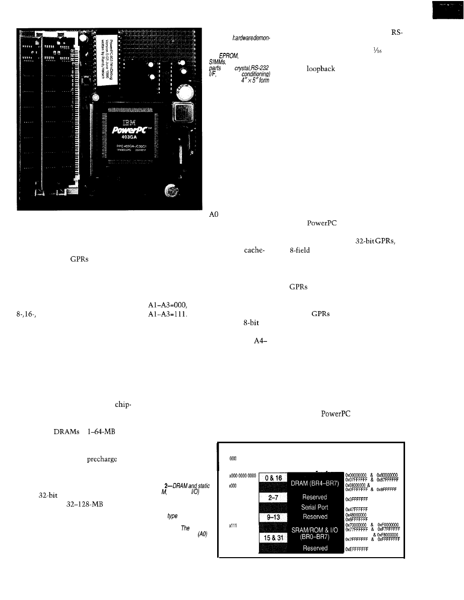
Photo l--The wire-wrapped
prototype
strafes a near-minima/
implementation with proces-
sor,
DRAM
and miscellaneous
(e.g.,
and power
contained in a
factor.
definite require-
ment when inter-
facing to most I/O
devices.
Figure 2 shows
the 403GA memory
map. Address bit
(the MSB) isn’t
used for external memory devices, so it
results in dual mapping for DRAM and
static devices. Both DRAM and static
memory decode split into two
ability regions, providing two groups of
chip-select areas (or bank-register mem-
ory regions) that can be selectively
cached for both memory types.
DRAM addresses need address bits
and static devices require
The BIU address-decode
logic effectively compares the
base address select (BAS) fields from
each bank register to address bits
Al 1 to generate the chip-select signals.
The DMA controller provides four
independent direct access memory
channels and includes BIU buffered
memory-to-peripheral, fly-by (BIU
bypass) memory-to-peripheral, and
memory-to-memory transfer modes
(supporting mismatched access time
memories). Memory-to-memory trans-
fers can also be initiated from software.
The built-in serial port provides
232 serial communication as well as a
high-speed mode timed from of the
processor clock. The serial port offers
internal
and auto echo modes
and may be a peripheral for DMA trans-
fers. Its control and status registers are
located at various offsets from address
0x40000000.
Asynchronous interrupts from exter-
nal sources and internal DMA, serial
port, and debug inputs are supported
through the on-chip interrupt control-
ler. Five external interrupt inputs are
individually programmable as active
high or low and edge triggered or level
sensitive. A negative edge-triggered
critical interrupt is also provided.
PROGRAMMING MODEL
Figure 3 shows the 403GA register
set. The
User Instruction Set
Architecture (UISA) is supported and
includes the thirty-two
an
condition code register (CR),
the fixed-point exception register (XER),
the link register (LR), and a branch-on
count (CTR) register.
O-3 1 are supported by nearly
all instructions. GPR 0 is used different-
ly for certain effective address calcula-
tions, and
1 and 2 are reserved for
the stack pointer and table of contents
(TOC) register by convention only.
The condition code register is di-
vided into eight 4-bit fields (CRO-7),
with each field containing LT, GT, EQ,
and SO bits. The XER provides carry
and overflow bits and serves as the
transfer byte count for load/store string
instructions. LR holds the return ad-
dress for the branch and link (b 1) in-
struction, the
CALL.
In true RISC fashion, the program-
mer (or compiler) has the freedom and
Addr bits AO-All
0000
0011
012345676901
Cache Reaion
Memory Type
Figure
(SRA ROM, and
memory
regions are fixed in
lower and upper address
ranges, respectively. Each
memory
can be
partitioned as cacheable or
noncacheable.
most
significant address bit
is ignored, resulting in a
double mapping across the
address space.
x00001111111
10000000
0x66000000
x00011111111
0001 0000 0000
0x10000000
001111111111
010000000000
0x40000000
010001111111
0100
10000000
011011111111
00000000
x1110111 1111
x11110000000
0x76000000
x1111111 1111
1001 00000000
0x90000000
11101111 1111
Circuit Cellar INK@
Issue 82 May 1997
2 3
Data Acquisition
new Value-Line has
uncompromising design features
and high quality components at
prices below the low cost guys!
Just
check out
the specs:
5500MF
8
channels
A/D,
16 digital
Counter/Timer
H i g h S p e e d
8 channels 12-bit
DMA
M u l t i - F u n c t i o n D M A
16 channels 12-bit A/D,
DMA, 16 digital
H i g h R e s o l u t i o n
5500HR
16 channels Id-bit A/D,
DMA, 8 digital
learn more:
voice
800-648-6589
Figure
403
supports PowerPC
user instruction-set architecture, including
thirty-two 32-M general-purpose registers
as well as several implementation-specific
peripheral-device control and
purpose registers to manage
features.
GPRO
0
0
0
PowerPC403
Specific
MSR
Device-Control
Registers
responsibility to manage the
(including the stack
pointer [rl by convention] and
LR) appropriately across proce-
dure calls. A leaf procedure
(i.e., one that doesn’t call an-
other procedure) need not save
the LR and may avoid this
extra overhead.
Special-Purpose
Registers
The count register (CTR) is
used by the conditional
on count instruction. It offers
a robust combination of decre-
ment count and branch on
CTR==O or CTR!=O and/or
condition code field (CR) bits.
Condition Register
XER Register
Link Register
LR
Count Register
CTR
A set of 403-specific device-control
the processor branches to the specific
and special-purpose registers are
exception vector based off the
ed for in- and out-of-core control and
tion vector prefix register (
EVPR
).
status. The device-control registers
offer eight BIU memory-bank control
INSTRUCTION SET
PowerPC
User Instruction
Set Architecture
G e n e r a l - P u r p o s e
Register
registers, bus error status, DMA con-
trol, external interrupt enable/status,
and an I/O configuration register.
The special-purpose registers use
debug breakpoint compare,
ity, memory write-protection bounds,
programmable interval timer, processor
version, time-base, and context switch
save/restore. These registers are
cessedusing
and
mf d
c
r (move to/from special-purpose/
device-control register) instructions.
The machine state register (MSR) is
a 3%bit register containing various
machine state bits. It is read and modi-
fied using mfms
r (move from/to
MSR).
The MSR includes the problem state
(PR) bit, external interrupt enable (EE)
bit, machine check (ME) bit, and little/
big
(LE) mode bits, among oth-
ers. The PR bit determines supervisor
or user mode.
When an exception or interrupt
condition occurs, the instruction ad-
dress register (IAR) and MSR are copied
to save/restore registers SRRO and
respectively. The MSR PR bit is
then changed to a supervisor state, and
Instructions are contained in a single
word with the high 6 bits speci-
fying a primary opcode. The remaining
bits are separated into various fields for
several different instruction formats,
including an extended opcode for many
instructions.
Most arithmetic, logical, and shift/
rotate instructions have both
register and register-immediate forms
such as:
add rD,rA,rB
rD,rA,simm
For the add immediate, if register is
0, then the sign-extended immediate
value is placed into (i.e., a load
immediate).
Several instruction forms employ
the convention “use the contents of
if != 0, otherwise use the value
zero.” Many instructions include a
record bit, Rc. It allows the instruction
to selectively alter the contents of
condition register field 0 (CRO).
The compare instructions include
register-register and register-immedi-
ate forms and offer selection of which
Issue a2 May 1997
Circuit Cellar INK@
condition register fields to alter
7). This example compares the contents
of GPR 5 to the value of 87 and sets
the appropriate condition bit in CR3:
cmpi
The conditional branch instructions
include five instruction fields-the
S-bit BO field specifying the conditional
branch type, the
BI field indicating
which condition register bit to test, a
branch displacement field, and
the AA [absolute address) and LK (pro-
cedure return link] fields.
The BO field offers combinations of
decrement CTR and branch if CTR==O
or CTR!=O, branch if bit BI in the con-
dition register is true false, and
branch always.
For example, in order to decrement
CTR and branch and link [i.e., save the
return address) to the subroutine at
absolute address 0x100 if CR1 indi-
cates less than or equal and the
CTR!=O, use:
Various extended branch mnemon-
ics provided by the assembler allow
simplifications such as:
beq
which branches to relative address
1 a be 1 1 if the EQ bit is set in CRO.
Most conditional-branch forms also
support a branch-prediction bit that
enables the programmer to indicate
the branch’s usual path. The processor
prefetches instructions down the speci-
fied taken or not-taken path.
For example, to indicate that a con-
ditional branch is usually taken, use:
bne+ label2
Load and store effective addressing
includes both indexed and direct forms
with or without update. Example for-
mats are:
Our Di
40 M
Sampling Oscilloscopes have 20 or
z maximum sampling rates with 8-bit
resolution. Both
have
32 Kbytes of storage; 7
sampling depths; 24 sampling rates; 6 input
voltage ranges; and multiple trigger
20 MHZ $
Our Logic Analyzer has 16
channels with
compatible logic inputs.
The maximum sampling
rate is 40 MHz with 6
internal clock rates and an
external clock input with +
or
going slope.
The
internal trigger
setup
allows bits to be low, high
or disabled. An external
logic level trigger is
provided as well as the
ability to trigger from our
DSO. The internal storage
is 32 Kbytes with 7
sampling depths and 3
trigger position options,
Units can be chained
for
larger data widths.
$199
26
Issue a2 May 1997
Circuit Cellar
lwz
stwx
The first instruction loads the word
at the specified effective address into
register
and the second stores the
word in register to the specified
effective address. Effective addresses
are calculated as:
l
displacement (d) form:
if == 0 b <= 0
else b
EA b +
l
indexed form:
if == 0 b <= 0
else b
EA <= b +
For update forms, the calculated
effective address EA is placed in regis-
ter after the memory reference is
complete (rA==O is invalid for update
forms).
Example load and store instructions
are:
lwzx
lwz
stw
stbu
The first instruction loads the word
at address
into r3. The second
loads the word at address
into
r12. The next instruction stores the
contents of r4 to memory address
0x1000. And, the last instruction stores
the least significant byte in to ad-
dress
and then puts the value
into register r3.
PROTOTYPE HARDWARE
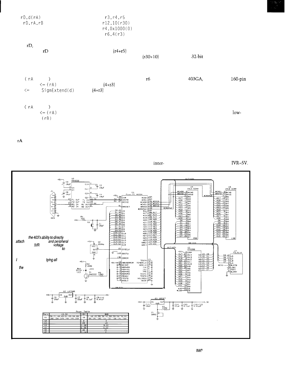
The prototype schematic, shown in
Figure 4, demonstrates a low-cost
403GA implementation. It isn’t de-
signed nor intended for production use.
The prototype
(see
Photo 1) com-
bines a byte-wide 32-KB (8K word)
EPROM containing initialization code
and a minidebugger with two 1 -MB
SIMM DRAM
S
, arranged as 1 M x 16
bits (5 12 K x 32-bit words), for program
and data. It includes an RS-232
face and a simple single-digit hexadeci-
mal display for initial debugging.
A minimal-cost system can also
easily employ a single byte-wide SIMM
by eliminating the second SIMM and
reprogramming the DRAM bank regis-
ter. Likewise, to maximize perfor-
mance, a
ROM and/or DRAM
configuration is a simple matter of
bank-register programming (and a few
extra bus wires).
The
available in a
plastic quad flat package (PQFP), is
attached to the Aries QFP-to-PGA
adapter and dropped into a surplus
AMP 15 x 15 PGA ZIF socket. The
cumulative adapter and (new) ZIF
socket cost nearly approaches
volume PC board NRE, but I chose the
adapter/socket and wire-wrapping
approach.
The 403 core operates at 3.3 V and
may interface either a 3-V system
exclusively or a mixed 3-15-V system
(as programmed by IVR, pin 39). This
implementation uses 5-V memory and
I/O devices and thus requires
Figure 4-A minima/ implementation
relies on
DRAM, EPROM,
devices. The
(interface
reference) pin enables interfacing
either mixed 345-V or exclusively 5-V
systems. To minimize initial debug time,
strongly recommend
unused
processor pins high or low as indicated
in processor specification.
Circuit Cellar
Issue a2 May 1997
27
I used an LM3 17 adjustable
regulator to provide the 3.3-V core
1
Initialize bank registers
supply. All 14 VDD power pins
2
Invalidate the
3
(and 19 GND pins) must connect
Enable EPROM cacheability
4
Test DRAM before data caching is enabled
to this supply. All unused inputs
5
Initialize
(interrupt) vectors
should be tied inactive. In particu-
6
7
lar, the manufacturing test inputs,
8
pins 23 and 24, must be tied low
9
and high, respectively.
10
11
Since memory-device width is
programmable, including the boot
ROM, some method must ini-
tially indicate the boot ROM’s
12
13
14
Initialize seriai port
Invalidate the
Enable DRAM cacheability
Set exception vector base address (EVPR)
Enable serial-port interrupts
Enable write-protection bounds
Initialize MSR
Set SRRO and
to simulate debug exception
Jump to debugger
width. This is achieved with the
Table
may
be somewhat less obvious, given the dual
on-chip
caches, memory-bank register programming, and
input (pin 11). Tying this
ability
used fhis sequence for my prototype
pin low selects an
boot ROM,
whereas tying it high selects a
boot ROM. Tying it to RESET (pin
91)
selects a
boot ROM.
The byte-wide boot/debug EPROM
requires the two least-significant ad-
dress bits (A30 and A31) to select the
byte within the
instruction or
data word. The
are not normally
required for
word references but
are provided for byte and half-word
accesses through signals WBE2 (pin
124) and WBE3 (pin
125).
BIU chip-select outputs
are controlled by bank registers
BR7, respectively.
l
CSO (pin 155) drives
the EPROM chip enable, and the
EPROM output enable pin is driven by
the processor *OE signal (pin 126).
bank 7) drives *RAS on both SIMM
When using DRAM devices,
processor outputs
are
controlled by bank registers
respectively (note the reverse number-
ing). The SIMM write signal is driven
by processor
(pin 138).
The single hexadecimal display
(TIL-311A) is a poor man’s alternative
to an in-circuit emulator or debugger
for initial system
It’s relatively
simple to debug and verify itself and
offers the capability of
sequen-
tial bring-up status while debugging
initialization code.
and BIU direct-attach memory
devices. Care must be taken to
invalidate the caches before use
and to properly initialize the
memory-bank registers before
attempting to access memory
outside the boot ROM region.
Table 1 shows the prototype ini-
tialization sequence.
First, I program the
bank registers to fully enable
EPROM, DRAM, and I/O accesses
and enable the device chip selects.
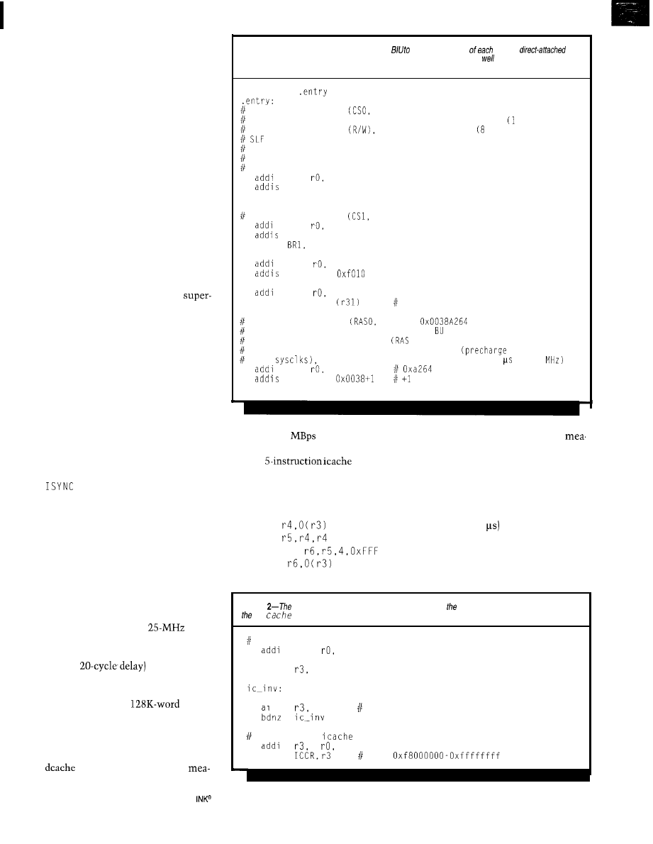
Listing 1 shows the assembly code
that sets up the bank registers.
The eight bank registers contain
various fields for base address selection,
hank size and usage, memory wait
states, ready enable, and other static or
DRAM specific settings.
For this implementation, hank
register 0 (BRO) is configured to select
the EPROM
is configured
for the hexadecimal display
l
CSl), and
BR7 is set to control the
DRAM
including refresh rate and cycle
times, attached to the
l
RASO memory
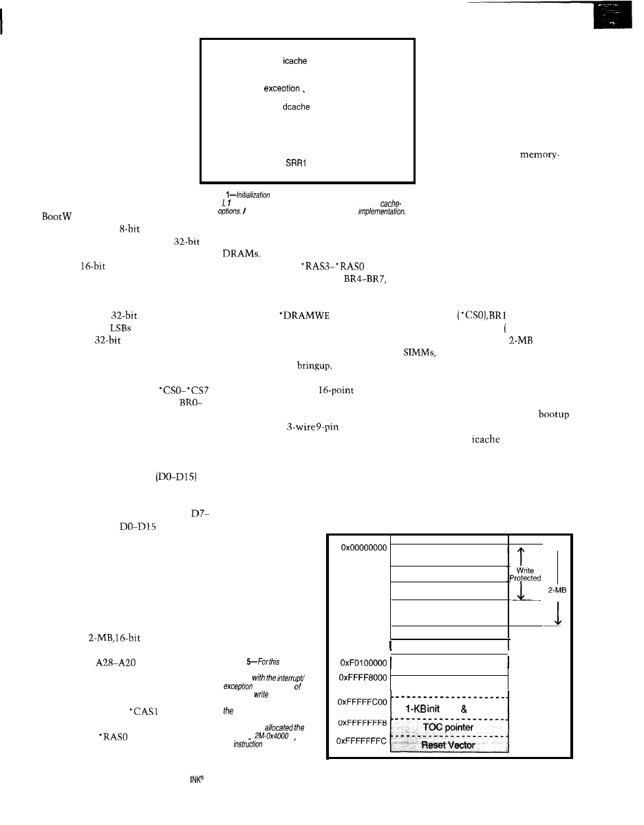
control pin. Figure 5 shows the result-
ing memory map.
Contrary to what you expect, the
high 8 (DO-D7) or high 16
data bits interface byte or half-word
wide devices. Data bits DO (MSB)-D7
(LSB) connect to EPROM data bits
DO, and data bits
connect to
the dual SIMM half-word DRAM.
DRAM multiplexed address bits
connect to SIMM address bits AO-A9
in a less than straightforward manner.
These processor address bits vary for
different bus and DRAM memory sizes
and are fully documented in the user
manual.
For the
DRAM con-
figuration implemented here, processor
address bits
and Al 7 connect
to SIMM address lines AO-A9. For a
16-bit DRAM configuration, processor
l
CASO (pin 142) drives MSB SIMM0
CAS, and processor
(pin 143)
drives LSB SIMM1
l
CAS.
Processor
(pin 146, the
DRAM chip-select pin for memory
28
Issue
82
May
1997
Circuit Cellar
Finally, the
D-shell
RS-232 interface uses a single-supply
MAX232 driver/receiver for processor
serial-port signals XMITD (pin 87) and
RECVD (pin 27). Note that processor
input ‘DSR (pin 28) is tied active.
INITIALIZATION SOFTWARE
Initialization
software is some-
what complicated by
the on-chip caches
Once the bank registers are config-
ured, I invalidate the unknown
contents of the instruction cache and
enable EPROM
cacheability to
boost initialization performance for the
remainder of the initialization sequence
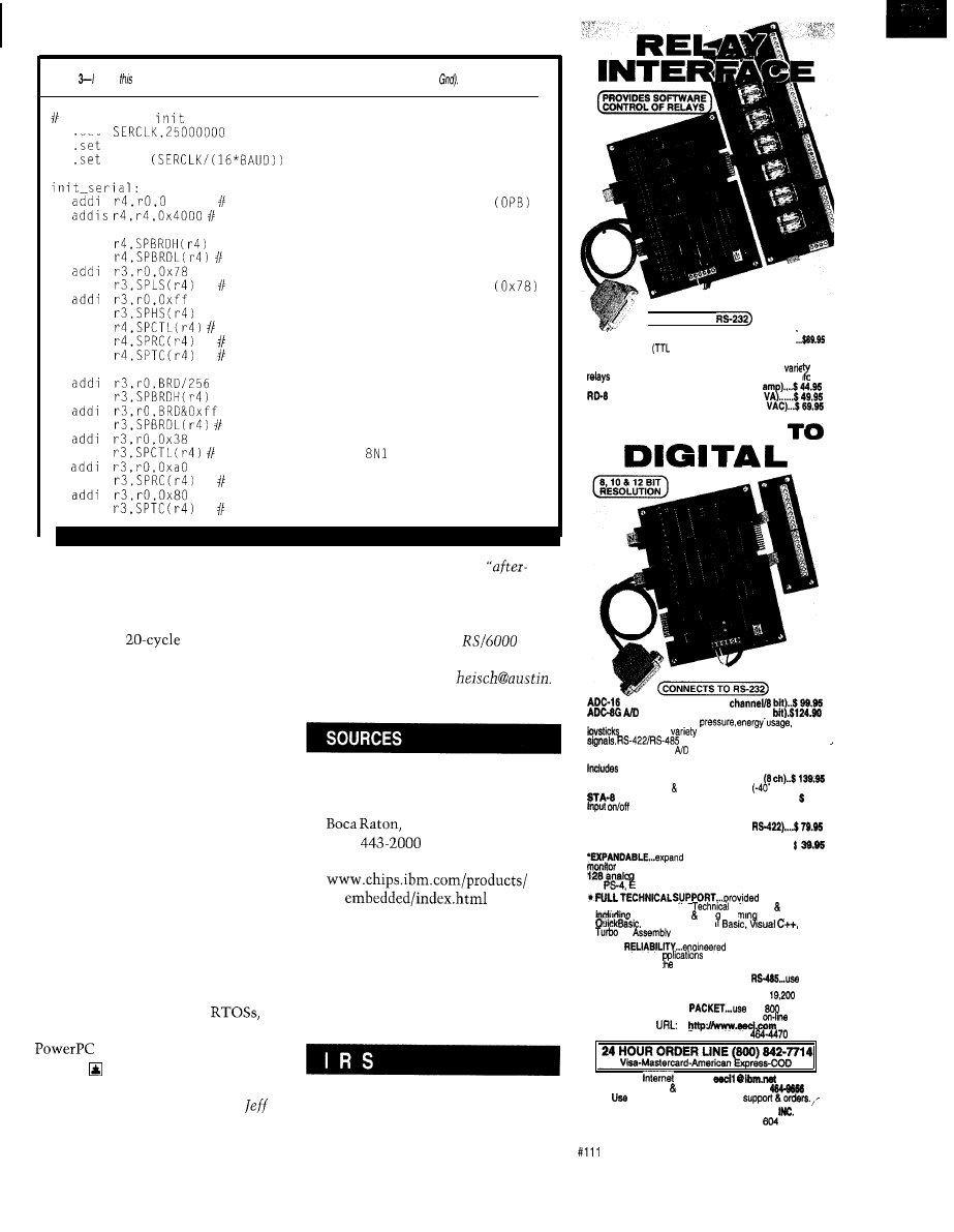
(see Listing 2).
At this point, and explicitly before
enabling DRAM data cacheability, I
verify DRAM integrity with several
Figure
implemen-
tation, fhe debugger shares
low RAM
vectors, bofh
which are
profecfed from
user-mode programs using
403 memory-profecfion
capabilities. User-mode
programs are
remaining
bvtes
for
and data
memory.
Debugger machine state
save area
0x00000100
0x00002100
Exception/interrupt vectors
Debugger stack area
0x00004000
User RAM
0x001 FFFFF
0x40000000
Serial Port
Hex debug display
32
KB x 8 (8K
word)
EPROM
data TOG
DRAM
memory test patterns. Once the mem-
ory is satisfactorily tested, I initialize
the exception vector prefix register
(EVPR) and exception/interrupt vectors
and configure the serial port control
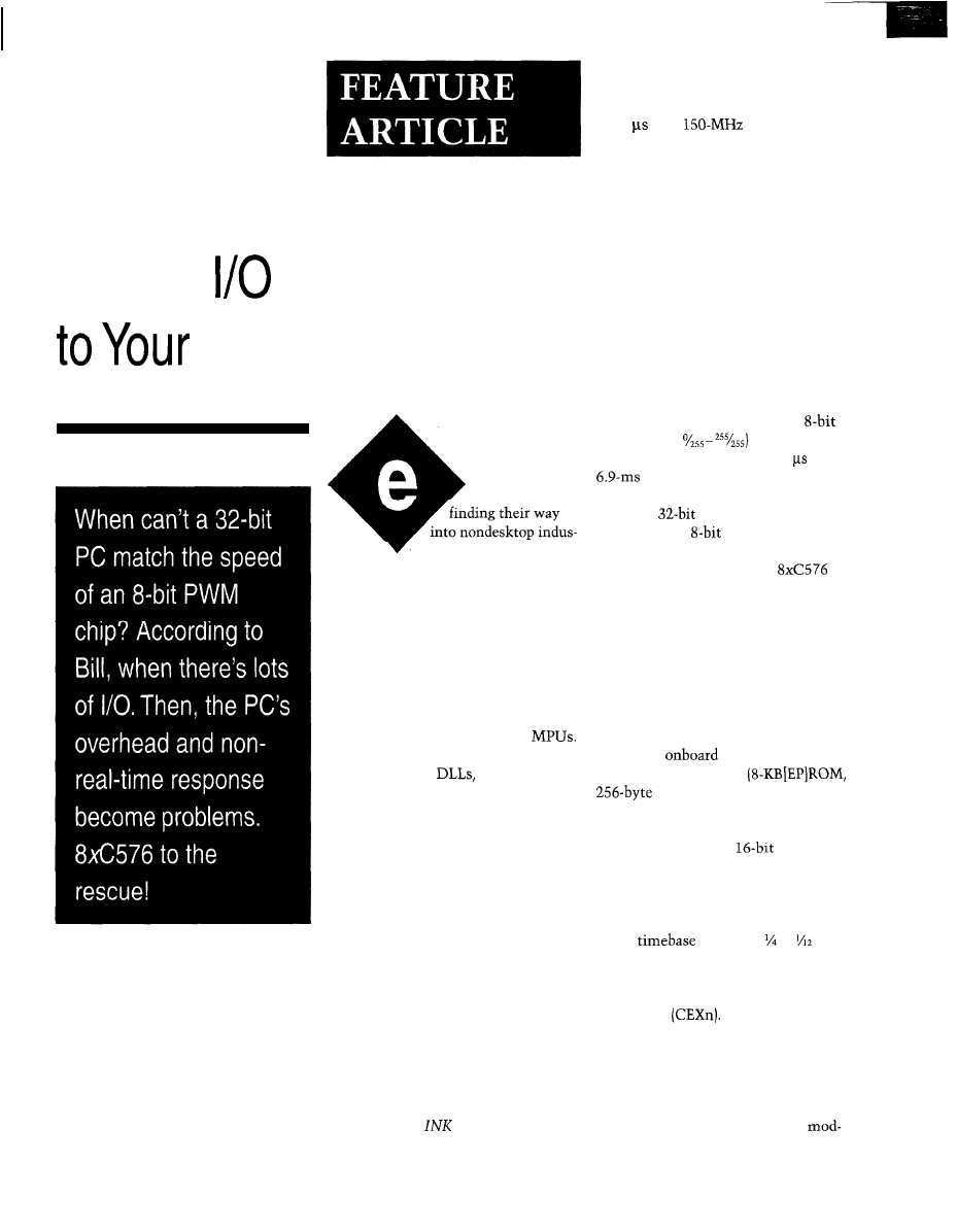
registers. The serial-port initialization
is shown in Listing 3.
The memory write-protection
bounds registers are initialized to catch
illegal user-mode program writes to
low-vector memory or past the end of
DRAM. The user mode MSR is initial-
ized and loaded, along with the IAR
(PC) of a dummy idle loop, into the
save/restore registers SRRl/SRRO to
simulate a debug exception. Control
then transfers from the assembler ini-
tialization to a C-level debug routine.
CONTEXT SYNCHRONIZATION
Since the 403 is a pipelined,
scalar processor, exercise due caution
when attempting certain operations
with CPU or memory context or se-
quence interdependencies.
For example, changing a memory
protection-bounds register for a mem-
ory area before executing a store in-
struction to that same area usually
causes a protection-bounds violation.
Ensure the protection-bounds update
is complete before attempting a mem-
ory write. Several CPU and memory
context synchronizing instructions
establish a known context including
and
EIEIO
(enforceinorder
execution of I/O).
PERFORMANCE
The primary disadvantage of the
reduced-cost, half-word DRAM con-
figuration implemented here is that it
requires two memory accesses per data
or instruction word reference.
Using a debugger developed for this
prototype, I downloaded and ran several
performance tests for a
imple-
mentation. Memory read access time
was measured at 808.4 ns per word (or
about a
for the given
DRAM configuration and bank-register
programming. The test read every other
fourth word from a
array,
thereby always missing the data cache.
This penalty can be halved via a
32-bit-wide DRAM configuration.
Sequential memory reads, missing the
on one out of four loads,
Listing l--The 403 bank registers configure the
the characteristics
specific
memory device, establishing memory size and fype, set-up and ho/d times, as
as DRAM interface and
refresh timings.
.globl
Set bank register 0
EPROM) = Oxff180700
BAS (base address select) = Oxff, BS (bank size) = 0 MB),
BU (bank usage) = 3
BW (bank width) = 0 bit),
(sequential line fill) = 0 (target word first),
BME (burst mode enable) = 0 (burst disabled),
RE (ready enable) = 0 (disabled), TWT (transfer wait states) = 7,
CSN = 0, OBN = 0, WBN = 0, WBF = 0, TH (transfer hold cycles) = 0
r3,
0x0700
r3, r3,
0xff18
mtdcr BRO, r3
Set bank register 1
hex display) = 0x01100200
r3,
0x0200
r3, r3,
0x0110
mtdcr
r3
r31,
0x0000
r31, r31,
ii r31 points to hex display
r30,
Oxf
stb
r30, 0
Write to debug display
Set bank register 7
DRAM) =
BAS (base address) = 0x00, BS = 2 MB, = RW
BW (bus width) = 16 bit, RCT
active to CAS active) = 1
FAC (first access timing) = 1, BAC = 0, PCC
cycles) = 1
(2.5
RAR = 1, RR (refresh rate) = 5 (7.68 at 25
r3,
-23964
r3, r3,
because low 16 is negative
mtdcr BR7, r3
sured at 18.9
or about five cycles
per load on average.
This
bound loop
verifies single-cycle instruction execu-
tion for given instructions with load
and store always hitting in the cache:
loop:
1
a
rlinm
st
bdnz loop
Average interrupt latency was
sured for both best- and typical-case
scenarios. The best response time of
17.5 cycles (700 ns) was measured for
interrupt-handler instruction fetches
and data references hitting the caches.
The typical-case latency measured
at 125 cycles (5
when the interrupt
handler always missed in both caches.
Both cases include six instructions of
extra overhead to generate an external
timing strobe.
Listing
insfrucfion cache contents are invalidated (using
i ccc i insfrucfion in a loop for each of
64 i
congruence classes) before if is enabled for use.
Invalidate the cache
r3,
64
mtspr CTR, r3
xor
r3, r3
iccci 0,
r3
r3, 16 next congruence class
Enable EPROM
cacheability
0x0001
mtspr
Make
icacheable
30
Issue
82 May 1997
Circuit Cellar
Listing
used serial-port initialization for the three-wire interface (Rx,
T
X
, and
Serial-port
set
BAUD,9600
BRD,
Base address to on-chip peripheral
Serial port (0x40000000) and 0 to low byte
stb
ii Baud rate div high = 0
stb
Baud rate div low = 0
stb
Clear serial port line status bits
stb
ii Clear serial port handshake status)
stb
Zero serial port control register
stb
Zero serial port Rx command reg
stb
Zero serial port T
X
command reg
stb
stb
Set serial port baud rate = 9600
stb
DTR = 1, RTS = 1,
stb
Enable receiver and RBR interrupts
stb
Enable transmitter
If you plan to call a C routine from
the interrupt handler or need to save
the entire machine state, interrupt
latency increases significantly (espe-
cially given a
cache miss
penalty). To maximize performance,
tune your code for both loads and stores
and instruction fetches to efficiently
use the caches and avoid cache-miss
penalties.
and encouragement of this
hours” project.
Randy Heisch is a senior engineer/
programmer in the IBM
Pro-
cessor and System Performance Group.
You may reach him at
ibm.com.
SIMPLY EMBEDDED SYSTEM
The 403GA provides a high-perfor-
mance, low-power RISC processor
with integrated on-chip caches and
support facilities. Its direct memory
attach bus unit makes it well-suited
for embedded applications.
My prototype implementation dem-
onstrates the simplicity and low parts
count possible for a minimum embed-
ded-controller system. IBM and select
independent vendors provide a full line
of software and hardware development
tools, including debuggers,
and
C/C++ compilers, supporting the
400 series of embedded con-
trollers.
Many thanks to Kaivalya Dixit,
Garelick, and IBM for their support
PowerPC 403GA
IBM
1000 NW 51 St.
FL 33432
(407)
Fax: (407) 443-4533
Aries QFP-to-PGA adapter
Digi-Key Corp.
701 Brooks Ave. S
Thief Falls, MN 56701-0677
(218) 681-6674
Fax: (218) 681-3380
404 Very Useful
405Moderately Useful
406Not Useful
( C
ONNECTS TO
AR-16 RELAY INTERFACE (16 channel) . . . . . . . . .
Two 8 channel
level) outputs are provided for
connection to relay cards or other devices (expandable
to 128 relays using EX-16 expansion cards). A
of
cards and relays are stocked. Call for more in o.
AR-2 RELAY INTERFACE (2 relays, 10
REED RELAY CARD (8 relays, 10
AH-8 RELAY CARD (IO amp SPDT, 277
A N A L O G
A/D CONVERTER* (16
CONVERTER’ (8 channel/IO
Input voltage, amperage.
light,
and a wide
of other types of analog
available (lengths to 4,000’).
Call for info on other
configurations and 12 bit
converters (terminal block and cable sold separately).
Data Acquisition software for Windows 95 or 3.1
ADC-BE TEMPERATURE INTERFACE’
Includes tan. block 8 temp. sensors
to 146’ F).
DIGITAL INTERFACE* (8 channel) . . . . . . . . . %.%
status of relays, switches, HVAC equipment,
security devices, keypads, and other devices.
FS-4 PORT SELECTOR (4 channels
Converts an RS-232 port into 4 selectable RS-422 ports.
CO.422 (RS.232 to RS-422 converter) . . . . . . . . . . . . . . . . . . .
your interface to control and
up to 512 relays, up to 576 digital inputs, up to
Ma
inputs or up to 126 temperature inputs using
X-18, ST-32 &AD-l6 expansion cards.
over the
telephone by our staff.
reference disk
test software pro rammin examples in
GW Basic, Visua
C,
and others are provided.
l
HIGH
for continuous 24
hour industrial a
performance in t
with 10 years of proven
energy management field.
l
CONNECTS TO RS-232, RS-422 or
with
IBM and compatibles, Mac and most computers. All
standard baud rates and protocols (50 to
baud).
FREE INFORMATION
our
number.
Fax or
E-mail to order. or visit our Internet
catalog.
Technical Support (614)
E-mail:
International Domestic FAX: (814)
for information. technical
ELECTRONIC ENERGY CONTROL,
380 South Fiih Street, Suite
Columbus, Ohio 43215.5491
Circuit Cellar INK@
Issue 82 May 1997
33
Bill Houghton
Add an Coprocessor
Embedded PC
mbedded PCs are
trial and scientific appli-
cations since there’s no doubt the PC
platform offers the most off-the-shelf
hardware and software options.
However, when it comes to real-
time data acquisition and control,
there are some skeletons in the PC
closet. All too often, it’s only after you
start rooting around that it becomes
clear that “real time” has a different
meaning on PCs than dedicated
Depending on the exact collection of
OS, BIOS, RTOS,
drivers, and
compiler, it can take a long time for
even the simplest I/O event to wend its
way between CPU and the real world.
Even the most streamlined PC set-
ups have a lot of overhead, imposing
dozens if not hundreds of microseconds
of overhead. Response time is poor and
subject to an annoying amount of jitter
(i.e., lack of determinism) due to every-
thing from cache effects to rude-neigh-
bor, cycle-hogging drivers.
If anything, the trend is getting
worse. For instance, Windows NT is
admired for achieving a degree of ro-
bustness required by embedded apps.
But, it so insulates the hardware that
it’s a major exercise to toggle a bit.
One recent series (“Embedded PCs
Go Industrial,”
75
and 77) mea-
sured the average latency associated
with NT’s built-in DPC (Deferred
Procedure Call) scheduling mechanism
as 27 for a
Pentium setup.
The worst-case response measured at
greater than 1 ms (or in the words of
the author, “essentially unbounded”).
While a few dozen microseconds
may not seem like much, it adds up
quickly. To paraphrase current wisdom,
“A few microseconds here, a few micro-
seconds there, pretty soon you’re talk-
ing
real
time.”
Consider the simple task of generat-
ing PWM output. Typically, a periodic
interrupt is handled by incrementing a
counter, comparing it to a value corre-
sponding with the desired duty cycle,
and toggling the output bit for matches.
A little math shows a simple
(duty cycle =
PWM is lucky
to run at 100 Hz (i.e., 256
x
27 =
cycle time) by the time a PC is
through with it.
That a
PC can’t match the I/O
handling of an
chip foreshadows
the solution. Use an MCU as an I/O
processor (IOP). The Philips
proves to be uniquely suited to the task.
‘576
TO THE RESCUE
Two issues come to the forefront
when choosing an IOP. Obviously, an
IOP needs lots of I/O for processing..
Though packaged in the 805 l’s
familiar 40-pin DIP or 44-pin PLCC
and QFP package, the ‘576 packs a lot
more stuff
than the original.
It’s double the memory
RAM) and has quite a few
high-value I/O functions added as you
see in Figure 1.
Along with a third
timer/
counter (the original ‘51 has two), the
‘576 adds a complete five-channel
Programmable Counter Array (PCA).
As shown in Figure 2, it comprises a
16-bit
(driven at or the
oscillator frequency from Timer 0
overflow or externally) feeding five
compare/capture modules, each with
its own pin
Each module can be independently
configured in compare or capture mode.
In capture mode, the pin becomes an
input which, on rising or falling edge
(programmable), latches the main
timer’s value into the associated
34
Issue
02
May
1997
Circuit Cellar INK@
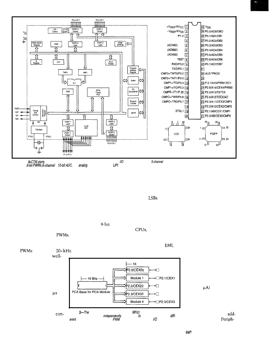
(ADINO)
(ADINO) P1.l
P1.3
P1.4
P1.5
XTAL2
“ s s
‘EANPP
‘PSEN
Figure l--The
with an enhanced 8051 core-CPU and adds significant functions, including
x
Id-bit PCA (Programmable Counter Array), hvo
dedicated
x
four
comparators, and a
(Universal Peripheral Interface).
ule capture/compare reg (both 16-bits).
In compare mode, the pin is an output
that toggles when the main timer
reaches the value programmed in a
module compare/capture reg.
The PCA is a powerful and speedy
(multimegahertz) unit, capable of many
tasks including interval timing, peri-
odic interrupt, PWM generation, and
watchdog timing. Nevertheless, it’s
supplemented with a dedicated watch-
dog timer and dual 8-bit
Un-
like a PC, which might struggle to hit
100 Hz with a software approach, the
‘576
run at up to
Though the various error specs (e.g.,
linearity, full scale, offset) range l-3
LSB, slow-changing signals can be
oversampled and averaged or the error
thrown away along with the two
by settling for 8-bit resolution.
The ‘51’s UART gets enhancements
as well, including framing error detec-
tion and automatic address recognition
for the
data mode. This mode,
offered on many vendors’
al-
lows simple multidrop networking by
relying on the ninth bit to signify that
the remaining eight bits should be
interpreted as a node address.
The ‘576 is equally
armed on the analog front
with a 6-channel IO-bit ADC
supplemented with four
analog comparators. The
ADC is capable of relatively
speedy conversion (48 in-
struction cycles, or 48 at
12 MHz), even though band-
width is usually limited to a
few kilohertz by slew rate
However, nodes must check all add-
resses for a software match. The ‘576
includes an address register with auto-
matic comparison, so it only interrupts
the CPU when a match occurs.
The ‘576 incorporates a number of
niceties addressing real-world design
concerns. The reset circuitry (active
low, as most chips are these days)
incorporates the watchdog timer along
with low-voltage and oscillator-failure
detection (allowed range: 6-l 6 MHz).
There are also modes to reduce
including cutting the clock drive
(reduces max clock to 12 MHz) and
turning off ALE (i.e.,
single-chip mode]. Low
active power
(a
little over
1 mA/MHz typical at 5 V)
is complemented with Idle
(0.5 mA/MHz) and Power
Down (5
modes.
With plenty of I/O pro-
cessing, all you need is a
mechanism for communi-
cation between the PC and
IOP. It’s the final ‘576
on-the Universal
Bits-1
PCA Timer/Counter
and sample-hold timing
Figure
PCA features high speed (up to 4
and resolution (16 bits). Each
of the five modules can be
programmed operate in a number of
straints.
modes, some of which (e.g.,
and edge capture) use an line (CEXC-4).
Circuit Cellar
Issue 82 May 1997
35
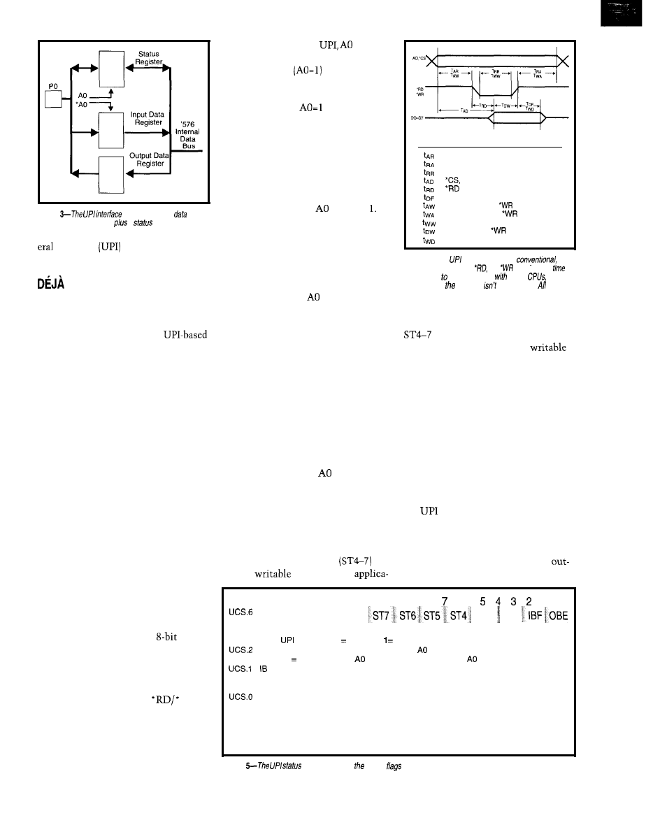
Figure
consists of one
register in each direction
a
register.
Interface
port-that’s makes
the PC connection.
VU
It’s
ironic that many don’t have a
clue what a UP1 is when almost every-
one uses one on a daily basis. Everyone,
that is, who uses a PC with a
micro on the receiving end of the key-
board cable.
Indeed, this is a classic example of
an MCU offloading the PC CPU of
mundane, time-consuming chores. No
doubt a Pentium, even burdened with
convoluted software, could manage a
keyboard’s clocked serial interface.
But, there’s also no question that it’s
not a bright idea. The fact that an MCU
with UP1 port made sense as an IOP
way back when reinforces the idea of
using one today for all sorts of other
I/O intensive and real-time tasks.
Fortunately, the UP1 is quite simple
to understand. Essentially, it’s a pair of
data registers [one in each direction)
and a status register (see Figure 3).
Together, they act as a communica-
tions mailbox between the ‘576 and PC.
It’s easiest to understand the way it
works by detailing port access from
each processor’s point of view.
The PC side accesses an
bidi-
rectional data bus (Port 0 of the ‘576)
and generates four control lines-•CS,
AO,
l
RD, and ‘WR. For the most part,
operation is straightforward, with *CS
enabling the UP1 port and
WR
strobing the data to/from the host.
Note that port access is quite fast as
shown in Figure 4. It is well able to
handle the historically relaxed (e.g.,
8 MHz) PC I/O expansion-bus timing.
36
Issue 82 May 1997
Circuit
Cellar INK@
For PC reads of the
works
as expected, selecting either the data
(AO=O) or status
registers.
Writes are a little trickier. While a
write with AO=O accesses the data
register, one with
does not di-
rectly write the status register.
Instead, it writes the data register
(i.e., same as when AO=O) and sets the
AF (Address Flag) bit in the status reg-
ister. In other words, writes from the
host always go to the data register, with
AF in the status register as the only
reflection of whether
was 0 or
Although it sounds odd, this scheme
makes sense. The decision not to allow
the PC to write the status register
directly is made purposefuliy to facili-
tate a robust protocol that minimizes
confusion about who’s doing what.
Simultaneously,
(accessible via
the AF bit of the status register) can
differentiate between subsystem com-
mands and data at the application level.
From the ‘576’s point of view, the
UP1 data bus is accessed as a byte (or
bit) addressable SFR (Special Function
Register address 80H) in the usual way.
Meanwhile, the UP1 status register is
also directly accessible via another SFR
address (86H).
Unlike the PC side, which can’t
write the status register (except the AF
bit via AO), the ‘576 has more write
The final piece of the puzzle is the
function of the various bits in the UP1
status register (see Figure 5). Besides AF
[the already described
flag], there’s
UE (UP1 Enable), IBF (Input Buffer
Full), and OBE/OBF (Output Buffer
Empty/Output Buffer Full).
Symbol Parameter
Min. Max.
‘CS,
A setup to ‘RD
0
‘CS,
A hold after
l
RD
0
l
RD pulse width
60
A to data out delay
70
to data out delay
60
l
RD to data float delay
5
l
CS,
A setup to
0
‘CS,
A hold after
5
‘WR pulse width
60
Data setup to
60
Data hold after ‘WR
5
Figure 4-The
interface is quite
relying on AO,
l
CS,
and
lines. Access
is
fast enough interface easily
most
and
if
ensures fhaf interface
a bottleneck. times
are in nanoseconds.
tion-specific flags. For example, the
UP1 handling PC keyboards defines
as parity and other error bits.
The UE bit is also always
by the ‘576 to enable or disable the UP1
interface. However, when the UP1 is
enabled, the key handshake flags AO,
IBF, and OBE/OBF are only affected by
hardware transactions.
Finally, IBF and OBE/OBF play the
critical role of handshaking transactions
across the UP1 data port. To keep things
Thus, during normal communica-
tions, the ‘576 doesn’t write these flags
since the hardware does it automati-
cally. And, in the interest of robust-
ness, it can’t write them. Of course,
during initialization and if things get
really goofed up, the ‘576 can disable
the
via UE to write protected flags.
access.
The upper four bits
are
straight, remember that input and
always
by the ‘576 as
put are from the ‘576’s point of view.
UCS.7
ST7 User-defined status bit
6
1
0
ST6 User-defined status bit
UCS.5 ST5 User-defined status bit
UE AF
UCS.4 ST4 User-defined status bit
UCS.3 UE
enable bit. 0 Disabled, Enabled
AF
Address Flag-contains the state of the
(Address) pin on the last write cycle.
0 Write cycle with
cleared, 1 = Write cycle with
set
F
Input Buffer Full Flag-set by hardware on the rising edge of a write
command to the alnput Data Register. Cleared by hardware on the
completion of a read cycle of the Input Data Register by the ‘576.
OBE’ Output Buffer Empty Flag-cleared by hardware on the completion of a
write cycle to the Ouput Data Register by the ‘576. Set by hardware on
the rising edge of the read command of the Output Data Register by the host.
*Note: This flag is OBE when read by the MCU but is inverted or OBF (Output Buffer Full)
when read by an external host.
Figure
register contains critical
enabling inferprocessor communication protocols
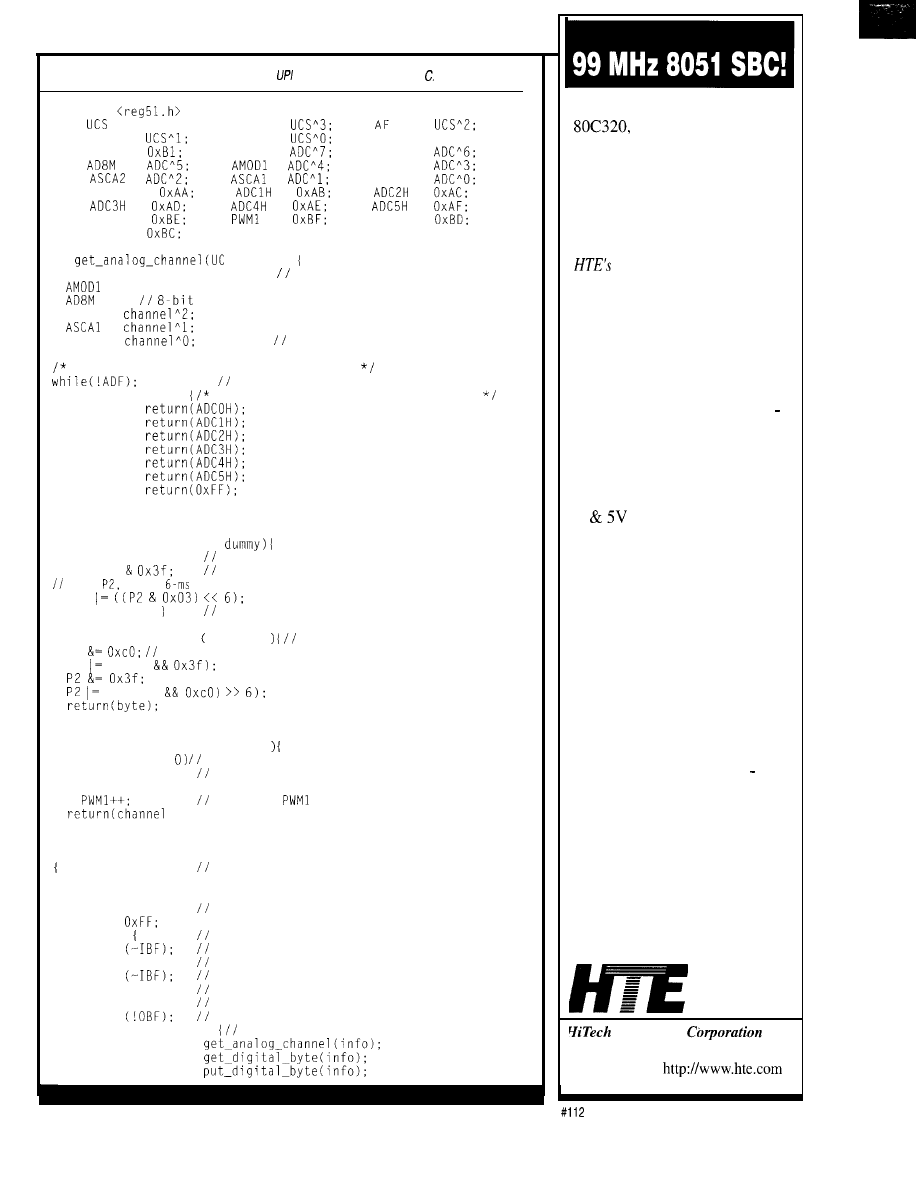
Listing l--This code demonstrates the use of the
on the ‘576 written in Franklin
#include
sfr
= 0x86:
sbit UE
=
sbit
=
sbit IBF
=
sbit OBF
=
sfr ADC
=
sbit ADF
=
sbit ADCE
=
sbit
=
sbit
=
sbit AMODO =
sbit
=
sbit
=
sbit ASCAO =
sfr ADCOH =
sfr
=
sfr
=
sfr
=
sfr
=
sfr
=
sfr PWMO
=
sfr
=
sfr PWMP
=
sfr PWCON =
UC
channel)
AMODO = 0;
Mode 0
= 0;
= 1:
mode
ASCAE =
=
ASCAO =
ADCE = 1; start conversion
poll ADF flag. Loop breaks when ADF = 1
wait for conversion to complete
switch (channel)
return ADC value by selected channel
case 0:
break;
case 1:
break;
case 2:
break;
case 3:
break:
case 4:
break:
case 5:
break:
default:
break:
UC get-digital-byte (UC
UC byte:
declare temporary variable
byte = P3
read P3 and strip the 2 M.S. bits
read
strip
bits, shift left 6 bits, OR with temporary var
byte
return (byte);
return result
UC put-digital-byte UC byte
clear current port value
P3
AND parm with mask, OR with cleared port value
P3 (byte
((byte
UC increase-pwm
if (channel ==
PWMO++;
else
UC channel
test channel parameter
increase PWMO
increase
void main 0
declare temp vars for cmd and info bytes
UC command:
UC info;
PWMP = 0x80:
initialize PWM controller
PWCON =
while(l)
wait for PC cmd re. when IBF flag is set
while
wait for the command
command = PO: read command byte. Clears IBF automatically
while
wait for next byte from PC
info = PO:
wait for information
PO = command: echo the command
while
wait for PC to read it
switch (command)
call approp funct, pass to parm
case 1: PO =
break;
case 2: PO =
break;
case 3: PO =
break:
(continued)
You’ve heard about the Dallas
and 805 1 compatible
CPU. It can really get the job
done fast, but you
need to get
started right now.
The 320SBC
features the ‘320 on a board that
is ready to go -- NOW.
32OSBC
features:
l
High speed 8051 Instruction
set, executes instructions up
to 3X as fast as a standard
805 1 at the same crystal
speed.
l
Cost effective: $179 for the
50 development version,
$149 for the -10 OEM
version in single qty.
l
Two serial ports: RS-232
l
Optional 3rd RS-232 serial
port can be used to free both
the ‘320 serial ports for your
application.
l
On board monitor eliminates
the need for an ICE in most
cases.
l
Development tools for C
or ASM
l
Production ready design
Now!
l
Special configurations
available that will reduce
cost and meet your specific
needs by including only the
features you need.
l
Compact size fits anywhere!
Equipment
,619) 566-1892
l
Fax:
(619) 530-1458
nfo@hte.com
Circuit Cellar INK@
Issue a2 May 1997
3 7
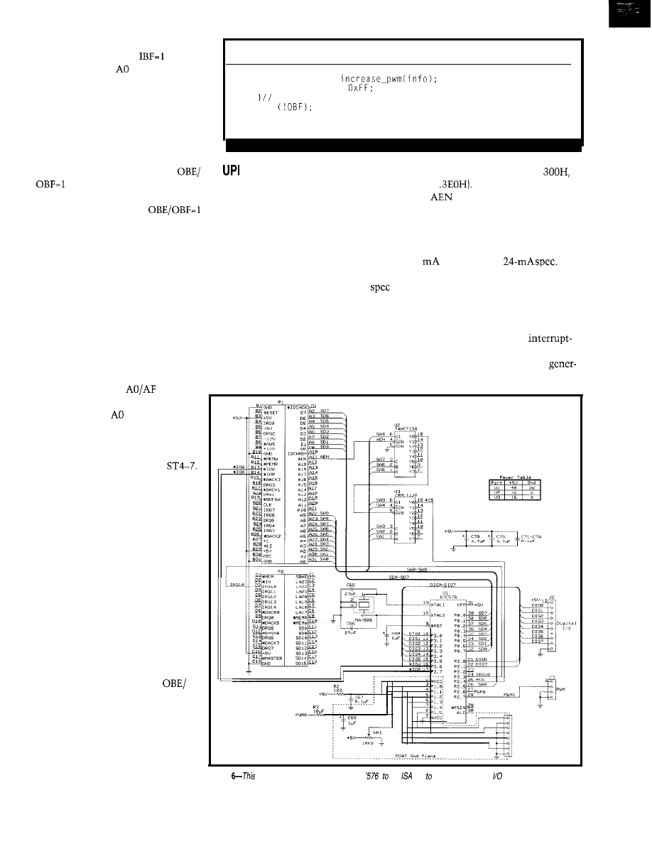
A PC write to the UP1 port (i.e., l CS
and * WR asserted) sets
(and AF
equals the state of
during the write).
A subsequent UP1 port read by the ‘576
clears IBF but doesn’t affect AF.
OBE/OBF is the only bit whose
definition isn’t straightforward. The
dual naming convention reflects the
fact that the sense of this bit is in-
verted between the ‘576 and host sides.
empty, so the ‘576 can write the next
From the ‘576 point of view,
byte. From the host side,
means the output buffer is
means the output buffer is full, so the
host should read the byte.
For coding purposes, you may want
to refer to OBE in the ‘576 software and
Listing l-continued
case 4: PO =
break;
default: PO =
break:
wait for PC to read information
while
IN ACTION
A sample application shows how
3EOH on 20H boundaries (i.e.,
320H..
Note that U2 is gated
OBF in the host code. In this case, a 1
in the bit is interpreted as a call for
action (i.e., host should read or ‘576
can write). Some may be more com-
fortable just choosing one name for
both host and ‘576 access and invert-
ing the bit’s polarity in software on
one side accordingly.
Beyond these basics, little protocol
is cast in stone. The
feature
need not be used, and if it is, the
interpretation of
is arbitrary. For
example, instead of differentiating
commands and data, the AF flag can
simply transfer a ninth data bit or act
as an auxiliary status bit like
is I/O addressed at ports 300H (data)
the UP1 facilitates the design of a PC
practical matter, the drive is sufficient
and 301H (status), which the ISA
with
to prevent unintended access
considering the historical progression
plug-in IOP. The design in Figure 6 uses
allocates for prototype cards, so the
of modern PC designs with the trend
during DMA cycles.
addresses aren’t likely already used.
the CPU, some address decode logic,
towards more logic on the motherboard
Should different addresses be required,
Though the UP1 interface presents
and less in the slots.
and little else to implement an ISA
simply choose another output from the
no timing problems for leisurely ISA
For experimenting with
decode logic.
plug-in.
driven protocols, this design wires a
The first decoder’s outputs (U2)
I/O cycles, the ‘576 can only deliver
‘576 output bit (Port 2, bit 3) to
address the board between 300H and
From the PC point of view, the UP1
ate an interrupt to the PC.
15
of the official
As a
Notice that the basic UP1 proto-
col is quite passive. That is, the PC
and ‘576 aren’t forced to rely on
possibly disruptive means (e.g., in-
terrupts, DMA) to communicate.
The ‘576 is the master in the
sense that it can enable or disable the
UP1 and directly set the flags. But,
the UP1 port can’t speak unless spo-
ken to by the PC. Similarly, there’s
nothing the PC can do to the ‘576
except send data which the ‘576 is
under no obligation to process.
Going beyond cooperative poll-
ing-type arrangements is completely
up to the designer. On the ‘576 side,
either or both of the IBF and
OBF bits can be programmed to
generate an internal interrupt
(whose priority, high or low, is indi-
vidually programmable as well). To
get the PC’s attention, just use a
‘576 port bit to output an interrupt
request to the PC.
38
Issue a2
May 1997
Circuit Cellar INK@
Figure
application example connects the
the bus create a PC plug-in coprocessor.
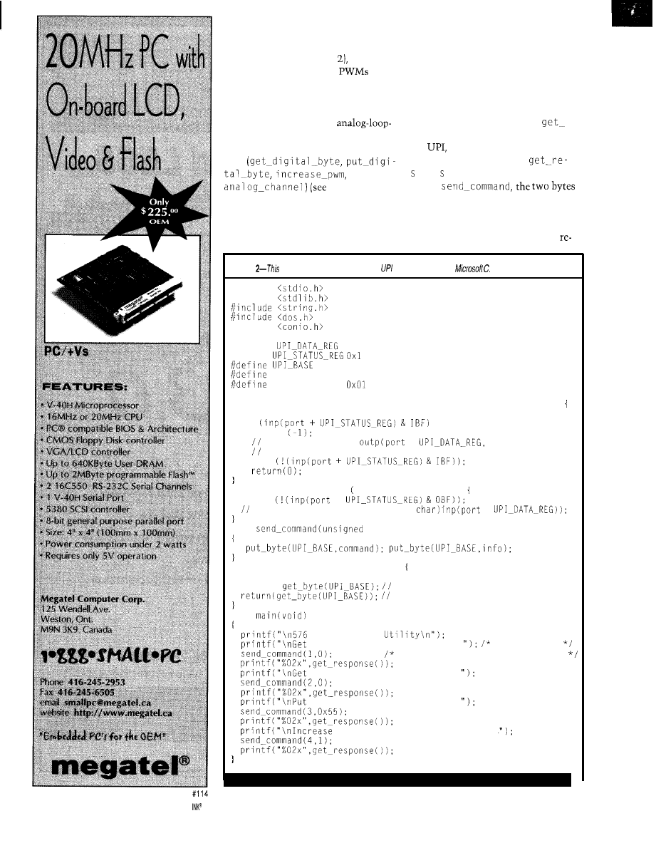
Eight bits of digital I/O (six from
Port 3 and two from Port four of the
A/D ports, and one of the
are
brought out to connectors. The second
PWM is configured as a DAC using an
RC filter and fed back to the fifth A/D
port to gain a convenient
back test capability.
The ‘576 code starts with four func-
tions
and
g e t _
Listing
1).
As
their names imply, they let the PC
The ma i n module simply waits for
the PC to issue the command and
performs the appropriate action. For
the read commands (digital and analog],
it returns the requested data.
On the PC side, the two functions
(see Listing 2) put-byte and
byte handle byte transfers to and from
the
respectively. Two other func-
tions, send-command and
pon e, assemble two-byte messages.
For
consist of the command and parameter.
request that the ‘576 read or write eight
For get-response, the first byte is a
bits of digital I/O, increase the PWM
dummy value (the echoed command),
value, or read the ADC.
and the second contains returned
Listing
code for the PC accesses the
pod and is written in
#include
#include
#include
#define
0x0
#define
0x300
IBF
0x02
OBF
unsigned char put-byte (unsigned short port, unsigned char data)
unsigned short dummy;
if
return
576 busy? dummy =
+
data);
send a byte, wait until 576 has read it
while
unsigned char get-byte unsigned short port)
while
+
wait for byte return ((unsigned
+
void
char command,unsigned char info)
unsigned char get-response (void)
unsigned char dummy:
dummy =
get the response
return the info byte
void
UP1 Interface
Analog Channel01 00 returned
send command
display result on sdtio (screen)
Digital Byte 02 00 returned
Digital Byte 03 55 returned
PWM
04 01 returned
40
Issue 82 May 1997
Circuit Cellar
for
get-anal
and
gi
ma i n
issues these four commands
sequentially and displays the results
onscreen. For testing digital I/O com-
mands, the PC first directs the ‘576 to
read the eight bits and then writes
to them. Probing the pins verifies the
alternating bit pattern output (i.e.,
or pull bits high or low
and see the results on the PC screen.
For the analog-loopback check, each
run of the PC program increases PWM.
Put the program in a loop and watch
the A/D input (at
resolution) value
cycle
from 00 to FF repeatedly.
MORE IS POSSIBLE
This example illustrates one
interface and protocol. Obviously,
level I/O commands can also be handled
with plain analog and digital I/O chips.
Full exploitation of the IOP calls for
high-level commands that offload a
large portion of the PC processing and
real-time burden. Then, instead of just
reading the ADC, it performs higher
level tasks (e.g., averaging multiple
readings or limit-checking the input).
Similarly, instead of just increasing
the PWM output, the ‘576 can autono-
mously perform complex waveform
generation. The goal is to fully offload
the PC of high-speed and short-latency
I/O tasks, freeing the main CPU for
ever-more complex application pro-
cessing.
Bill Houghton is a senior applications
engineer at Philips Semiconductors.
He has over 12 years’ experience spe-
cializing in the
microcontroller
family. You may reach him at bill.
Philips Semiconductors
8 11 E. Arques Ave.
Sunnyvale, CA 940883409
(408) 9915207
Fax: (408) 991-3773
407 Very Useful
408 Moderately Useful
409 Not Useful
116
“We’re impressed by the
documentation and the readability
You
Should
Choose Embedded
BIOS, Too
of
the code. M. Ryan
BIOS, DOS, Flash Disk With One Low Royalty
“We
pleased with the
General Software BIOS and look
Instant Boot, Console Redirection, Much More
forward to working
you to bring
to market. R.
Expert Support with Guaranteed Response Time
Embedded BIOS is well-structured
We Work Closely With
AMO, Intel,
and documented, end technical
to Deliver you a Proven, Tested, Feature-Packed BIOS
support at General
is
Millions of Units Already Licensed
sure we
mode the right
decision to buy our BIOS from
Kit Includes:
General Software
Complete Source Code
“Embedded BIOS is really
Binary Configuration Program
embedded PC designs.
You were absolutely right.
Quick Start + Over 600 Pages of Printed Documentation
3 ’ 2 0
108th Ave. N.E.. Suite 400
W A 9 8 0 0 4
T e l : 2 0 6 . 4 5 4 . 5 7 5 5 . Fax: 206.454.5744 . S a l e s : 8 0 0 . 8 5 0 . 5 7 5 5
E-Mail:
With Cimetrics’
you can link together up to 250 of the most popular and
microcontrollers
B-Bit
is:
Fast-
A high speed
baud) multidrop
master/ slave
network
Compatible with your
microcontrollers
Reliable- Robust 16-bit CRC and sequence
number error checking
.
Efficient-
Low microcontroller resource
requirements (uses your chip’s built-in serial
Friendly-
Simple-to-use C and assembly
language software libraries, with demonstration
programs
. Complete- Includes network software,
network monitor, and RS-485 hardware
.
is an asynchronous
adaptation of IEEE 1118
5 5 T e m p l e P l a c e
l
Boston, M A 0 2 1 1 1 - 1 3 0 0
l
Ph 617.350.7550
l
F x 6 1 7 . 3 5 0 . 7 5 5 2
Circuit Cellar
Issue 82 May 1997
43
Art Sobel
Embedding the ARM7500
Part 1: The Chip and Development Board
computer on a chip and
the design of a simple ARM7500 appli-
cation board. I also discuss the ARM
version of the
that’s been ported to the ARM7500.
The ARM7500 is a low-power,
performance, single-chip computer
centered around an ARM microproces-
sor core. This direct descendent of the
Acorn Archimedes computer contains
the original four-component custom
(i.e., CPU and memory, I/O,
and video/sound controllers) as well as
4 KB of cache memory, LCD support,
and PC peripherals.
In 1988, the original Acorn
was produced on a
CMOS pro-
cess. The current part is made with
VLSI’s
CMOS process.
Processor speed also improved. The
original chip ran at 8 MHz, producing
6,000 Dhrystones. The ARM7500 zips
along at 40 MHz, producing 59,000
Dhrystones. The raw performance is
similar to a
but without
the heatsink.
To maximize the potential of the
ARM processor macrocell, the
7500 contains memory and I/O control
on-chip, enabling external memory
devices and peripherals to connect
directly with minimal external compo-
nents.
Acorn designed the ARM7500 into
its low-cost
A7000, as well as
the Digital TV
box. It is also
present in Oracle’s Network Computer.
And, it’s in Teknema’s Easy Rider
Internet Browser Computer and
call America’s Webster.
ARM7500 has been in production
since July 1995. Figure 1 shows the
main components.
CPU CORE
The ARM704 CPU core powers the
ARM7500. It contains the ARM7 CPU
as well as 4 KB of cache, MMU, and
write buffer.
The cache is partitioned as a
way set interleave design. For each set
of upper address bits, four entries (each
containing four words) can be stored in
the cache. If all possible entries are
filled, one is randomly discarded and
overwritten.
MEMORY CONTROLLER
The memory controller interfaces
with the three types of memory in the
system-DRAM, ROM, and I/O. Most
of the memory is DRAM, and the
ARM7500 can directly control up to
256 MB, far more than is needed for
most applications.
DRAM is the common fast-page
variety with RAS before CAS refresh.
It can be configured to be 16 bits wide
for cost-sensitive applications, but that
halves its bandwidth capability.
High DRAM bandwidth is of utmost
importance when simultaneously
servicing a fast CPU and high-density
display. DRAM timing is directly con-
trolled by the MEMCLK input, which
can be asynchronous from the CPU
cache clock.
The ARM7500 handles ROM in
and 32-bit widths. ROM timing has a
programmable number of MEMCLK
cycles. Flash memory can be accom-
modated as a peripheral on the I/O
bus, but later versions have flash in
ROM space.
Many I/O cycles are similar to ROM
cycles, but some can be extended with
the WAIT pin. Although the external
I/O data bus is only 16 bits wide, it can
extend to 32 bits with external latches.
Issue 82
May
1997
Circuit Cellar INK@
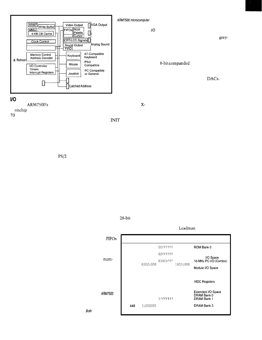
DRAM
Address
DMA Controller
LCD Output
Digital Sound
Purpose
Memory
Data
Peripheral Data
In the
full complement
of
peripherals, there are about
programmable registers in the I/O
and memory controller (52 in the inter-
nal I/O controller and 18 DMA control-
ler registers).
Of the 11 open-drain I/O pins, 8 can
be external interrupt pins. The key-
board and mouse interfaces have two
open-drain pins for data and clock
which support the AT and
mouse
interface protocols.
Three DMA regis-
ters for the video set
up a circular buffer
that can be used for
hardware scrolling.
However, this fea-
ture is not so useful
with windowing software (e.g.,
Windows or a Web browser).
The cursor DMA is simpler and has
a single DMA
register. Sound
output requires dual DMA pointers
that create a continuous datastream to
the sound circuits.
Four pins are used for the joystick
interface, which supports the PC-type
variable resistor joysticks with capaci-
tors on the motherboard. Each pin
connects to an open-drain clamp tran-
sistor and a comparator.
When the open-drain transistor is
turned off, a 16-bit counter operating at
2 MHz starts. It is stopped by the com-
parator being triggered as the variable
resistor charges the attached capacitor.
An interrupt is generated when the
programmed combination of compara-
tors is triggered.
This interface can also be used as
four general-purpose timers measuring
rising-edge timing from external sen-
sors (e.g., a sonar detector).
DMA
Three DMA channels supply the
internal video, video cursor, and sound
controller with data from the DRAM.
Fast-page DRAM has a limited total
bandwidth, so the display robs the CPU
of memory cycles. Beyond a certain
point of display resolution, either the
display or CPU is starved for memory
cycles.
Figure
l--This diagram of the
shows the main operational
blocks-CPU, memory
controller, video controller,
controller, and embedded-PC
peripherals.
VIDEO AND SOUND
DEVELOPMENT BOARD
The video and sound output logic is
derived from VIDC (video controller)
chips. The VIDC connects to the data
bus with one chip-select signal and
several DMA write signals.
The written control data contains
the address of each programmable
register and the controlled function’s
data field. With this configuration, the
registers are just write only.
When I contemplated the design of
an ARM7500 development board, I
tried to include support for all possible
uses customers might have for the
part. Any one application might have
features removed or modified. The
ultimate use was a Unix workstation.
Other applications were subsets.
There are 34 dedicated registers for
video functions and 10 sound-control
registers. Also included are 256 indi-
vidually addressed
video-palette
registers. They are split into 8 bits for
red, green, and blue entries for each
One important consideration was
the mechanical configuration of the
board. I decided that the best configu-
ration was a direct fit into a flat PC
workstation chassis.
The positions of the connector and
mounting holes were adjusted to fit a
case from
Electronics. The
logical color.
Separate
exist for regular
video, cursor,
and sound data.
The large
Table l--The memory
map for the
has assigned physical
addresses. These are
remapped by the Demon
(Debugging Monitor).
maps are shown.
ber of registers makes the video param-
eters very flexible.
The VIDC also supports LCD panels.
The video controller supports a variety
of single and dual panels, binary,
scale, and color. Some panels require
external circuitry for panel protection
and interfaces.
The old Acorn computers had an
audio DAC built into
the VIDC. Preserving that legacy, the
VLSI ARM7500 adds support for exter-
nal 16-bit CD-ROM serial
MEMORY MAP
The addresses in Table 1 are physi-
cal addresses encompassed in 29 of the
32 address bits. Their position in mem-
ory may be moved to other virtual
locations.
Thus, even in the debugging moni-
tor (Demon), the DRAM is moved to
lower addresses to allow for exception
vector programmability.
Megabytes From
To
Demon Map Description
0
00000000
20000000
16
01000000 Olffffff 21000000
ROM Bank0
32
02000000
disabled
Reserved
48
03000000 0300ffff 10000000
Module
03010000
10010000
0302ffff
Reserved
03030000 0303ffff 10030000
03040000 031fffff 10040000
Reserved
03200000 0320ffff 10200000
IOC Registers
03210000 033fffff 10210000
Simple I/O
03400000 034fffff 10400000
03500000 03fOffff 10500000
Reserved
64
04000000 07ffffff disabled
Reserved
128
08000000 Offfffff 18000000
256
10000000 13ffffff 00000000
320
14000000
disabled
384
18000000 lbffffff disabled
DRAM Bank2
lfffffff disabled
512
20000000
memory map
repeats
Circuit Cellar INK@
Issue 92 May 1997 4.5
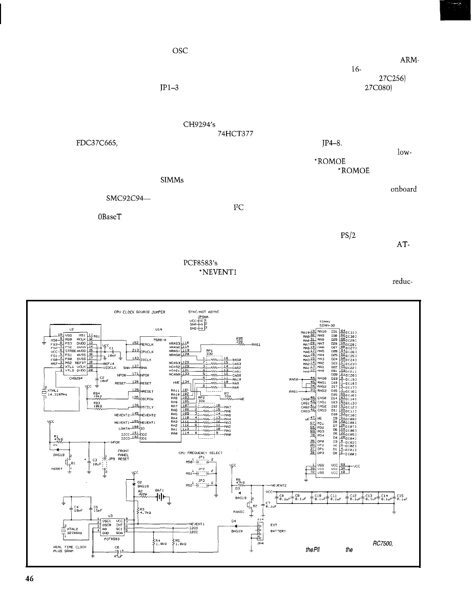
case
has a 100-W power supply, hold-
ers for 3.5” floppy and hard disks, and
a wide, open, back panel with room for
many I/O connectors.
A board extender inserts into an ISA
slot and offers three other slots at right
angles. The motherboard only includes
that ISA slot. The space usually allo-
cated to slots is taken up by peripher-
als that used to fit into I/O cards.
Two important chips complement
the CPU. For the I/O combo chip, I
chose the SMC
but simi-
lar chips from other suppliers can be
used. The ‘665 contains two 550-type
serial ports as well as a bidirectional
parallel port, high-density floppy con-
troller, and IDE chip select.
The second chip-the
is a self-contained Ethernet controller
that directly handles 1
with a
transformer filter.
THEORY OF OPERATION
Figure 2 shows the first page of the
RC7500 schematic. The board clocks
are generated by a Chrontel CH9294. It
14.318MHz 4x color-burst frequency
used on PC motherboards to generate
the
signal for the expansion slot.
The three 7500 clocks connect to
the MCLK output of the CH9294. This
output is programmed by the jumpers
to be nominally at 65 MHz.
Therefore, the processor cache clock
will be 32.5 MHz after being divided
by 2 internally.
The
VCLK output is
programmed by a
register.
This clock provides a video clock for
VGA and SVGA pixel rates and goes
back into the VIDC section of the
ARM7500. Standard 72-pin, 32-bit
are used for main memory.
The PCF8583 became the real-time
clock chip because the ARM7500 has
two pins dedicated for
operation. It
offers additional battery-backed RAM
for saving system hardware data. The
RC7500 has room for a 3-V lithium
battery or a standard external PC
motherboard battery.
The
alarm signal con-
nects to the
pin. The panic
interrupt can wake the ARM7500 from
power-down modes.
The RC7500 is equipped with four
ROM/EPROM sockets. Since the
7500 can support
and 32-bit memo-
ries, as little as 64 KB (2 x
or
as much as 4 MB (4 x
of ROM
can be used.
So, anything from a boot loader to a
complete OS with many utilities can
be placed in ROM. Addressing of vari-
ous types of EPROM is provided by
jumpers
The ARM7500 generates the
going
signal, which, is con-
nected to the
pins. When an
external ROM emulator is hooked up
to the logic analyzer port, the
ROM can be disabled by pulling the
DISAROM signal high.
The ARM7500 has two electrically
identical keyboard ports assigned to
keyboard and
mouse connectors
as shown in Figure 3. These are
compatible bidirectional open-drain
serial ports.
Dual diodes and capacitors are used
provides three clocks, one being the
button connects to
l
NEVENT2. Either
for static protection and noise
Figure 2-h this schematic of the
you
see clock chip, calendar timer chip,
and DRAM.
Issue 82 May 1997
Circuit Cellar INK@
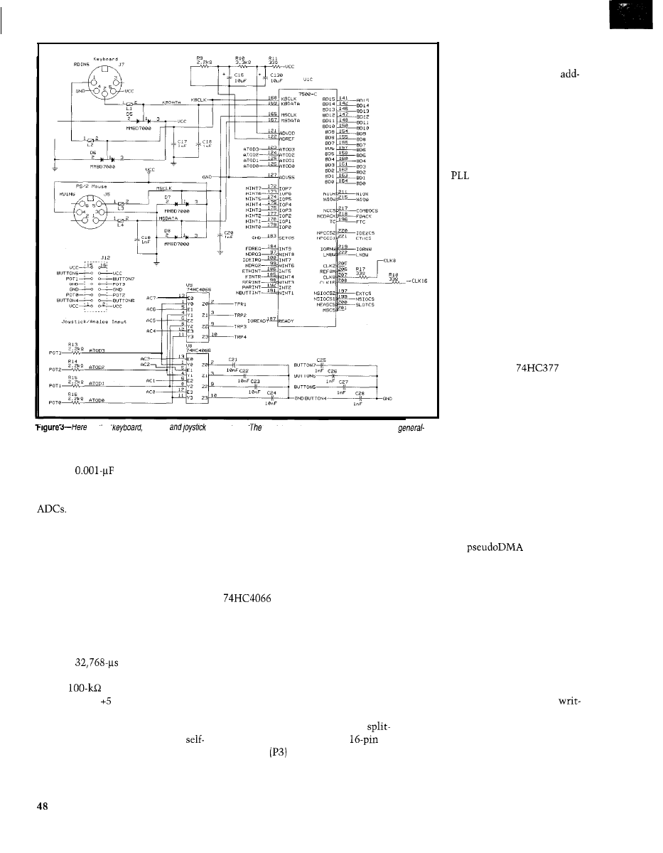
are me
mouse,
connecbons.
purpose timers.
joystick can be programmed for use as four
panel connected to the inter-
face. This connector also has
the signals for a genlock
on circuit.
The vertical sync resets
when the SINK pin is held
high. However, there’s no
such circuit for horizontal
sync. It must be achieved by
line locking with a dot-clock
and phase detector on
the horizontal sync pulses.
The sound output gener-
ated from the TDA1543
could have been connected to
a 3.5mm stereo connector. I
chose a more complicated
circuit, using the National
LMC1982 sound controller
IC, plus the LM2878 ampli-
fier SIP, which generates 5 W
per channel.
The LMC1982 is controll-
ed with a serial datastream,
using a minimum pin count
from an added
data
latch. The only problem left
is where to put the speakers!
Since this board is for
unique applications (or port-
ing old ones) for the ARM, I
tion. The bit rate on these pins is fairly
slow, so
caps do not affect the
signals.
The ARM7500 has four single-slope
Each pin has an open-drain
transistor and attached voltage compar-
ator controlling a 16-bit ripple counter.
When the transistor is off, the voltage
on the pin rises as current from a resis-
tor attached to the +5-V supply charges
a capacitor connected to ground.
When voltage rises to the compara-
tor threshold at 2 V, an interrupt is
signaled and the 16-bit ripple counter
stops. The counter is run from the
IOCLK divided by 32 [ideally 2 MHz),
giving a
maximum time
period.
The
joystick pots provide
the resistor to V. In a PC, they are
routed to an SE555 timer circuit timed
by the CPU with interrupts off for as
long as several milliseconds. The
timed ARM7500 A/D circuits prevent
having to turn the CPU interrupts off
for such a long period.
Issue
82 May 1997
Circuit Cellar INK@
These unique inputs are more versa-
tile than joystick-only ports. If an exter-
nal rising signal is substituted for the
resistor- and capacitor-formed slope,
the pins can be used for simple timers.
Distance to nearby objects can be
measured for four inputs simulta-
neously (up to 16’ at 2 ms per foot). To
be used as a timer, the capacitors are
switched out and pull-up resistors are
switched in to each A/D input with
analog switches.
The audio and video connections
are shown in Figure 4. I opted for the
higher fidelity of an inexpensive 16-bit
CD DAC [Philips TDA1543).
The ARM7500 supports direct-drive
RGB outputs into doubly terminated
75-R lines. I added protection diodes to
these outputs because CRTs can col-
lect static charges very easily.
LCD outputs for straight and
screen displays connect to a
connector
for convenience. Since
there is no standard LCD connector,
an adapter must be made for each LCD
provided an ISA-like plug (see
Figure 5). All signals to the slot are
buffered to protect the 7500. Most
existing boards can be made to work.
This board is not completely ISA
compatible, which would have required
a redesigned ARM7500. Principally,
the board only handles slave devices.
Only two
channels are
handled by FIQ interrupts. No byte
packing is done, so the designer must
know where the bytes are going in any
port. Software does byte packing and
unpacking. Slot addressing is carved
out of the expansion memory in several
segments for activating MEMR/W,
IOR/W, and DMA signals.
A 96-pin connector has a selection
of the bus signals for expansion into a
logic analyzer pod. It could also be
connected to a ROM emulator or
able control store. ROM, DRAM, and
many I/O operations can be decoded.
PORTS AND INTERFACES
The typical I/O devices found in a
PC are all compacted into Super IO or
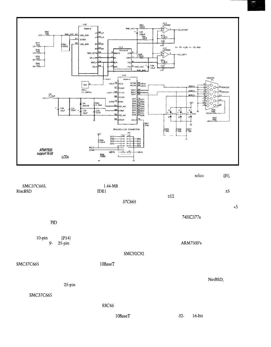
Figure 4-The
audio, video, and LCD
,
interfaces
stereo sound. Although
standard VGA is connected, the
require an
adaptor board.
combo chips.
I couldn’t resist these,
manufacturers shut down at the same
an
RJ-45 8-pin
connector
of
and neither could Acorn. We both use
time. The RC7500 chassis mounts a
which only 4 pins are used.
the
so software like
requires fewer rewrites.
There are two serial ports. Port 1
connects to a 9-pin subminiature D
connector (J2) that’s PC compatible and
also found in all other ARM develop-
ment boards. The same serial hookup
for VLSI and ARM
and PIE boards
can be used.
The second serial channel is termi-
nated by a
header
that can
be connected to a or
D con-
nector with mass-terminated wire as
found in many PC I/O boards.
The parallel port supported by the
is bidirectional and ECP
compatible. The proper driver supports
these IEEE-1284 interfaces. The paral-
lel port is terminated with a 26-pin
header that translates to a
D
connector with a short cable.
The
has a PC-compat-
ible enhanced floppy controller with
digital data separator. It directly drives
all normal floppy types up to 2.88 MB.
Unfortunately, all these floppy-drive
single
3.5” floppy drive.
is mapped in the combo’s
address space, and the chip selects are
produced by the
combo chip.
IDE2 is mapped in the simple expan-
sion space, so two different master
drives can operate simultaneously for
faster operation than a master/slave
configuration (although two masters
and two slaves can be supported). Usu-
ally, this is one hard drive and one
ATAPI IDE CD-ROM drive.
Ethernet is all the rage and fairly
inexpensive. The
supports
both twisted-pair and coaxial versions.
The
version uses shielded
twisted-pair wiring into star hubs.
With the proper software OS and
TCP/IP protocols, the RC7500 can be
made into a workstation that can coex-
ist in the same network with Unix
boxes and PCs-and onto the Internet!
The Ethernet local address is stored
in an
EEPROM that also has
room for the Host ID-if one is ever
needed. The
is terminated in
Power is provided by a standard PC
power connector, supplying the and
V needed by the motherboard and
expansion slot. A 4-pin disk-drive con-
nector can be used that supplies the
and + 12 V needed on the motherboard.
Two
control the LED bar
and the joystick input load program-
ming.
ARM7500 APPLICATIONS
The
range of features
makes it extremely flexible. It can be
programmed to optimize for high per-
formance, low power, or both.
The ARM has an eight-year history
in Acorn PCs. Its low cost and integra-
tion offers places like schools a lower
price computer. With
the
ARM offers display nodes for campus
networks.
Power-management circuitry and
the power-efficient characteristics
makes the chip particularly suitable
for low-power portable applications.
Since and
wide memory
5 0
Issue 82
May
1997
Circuit Cellar INK@
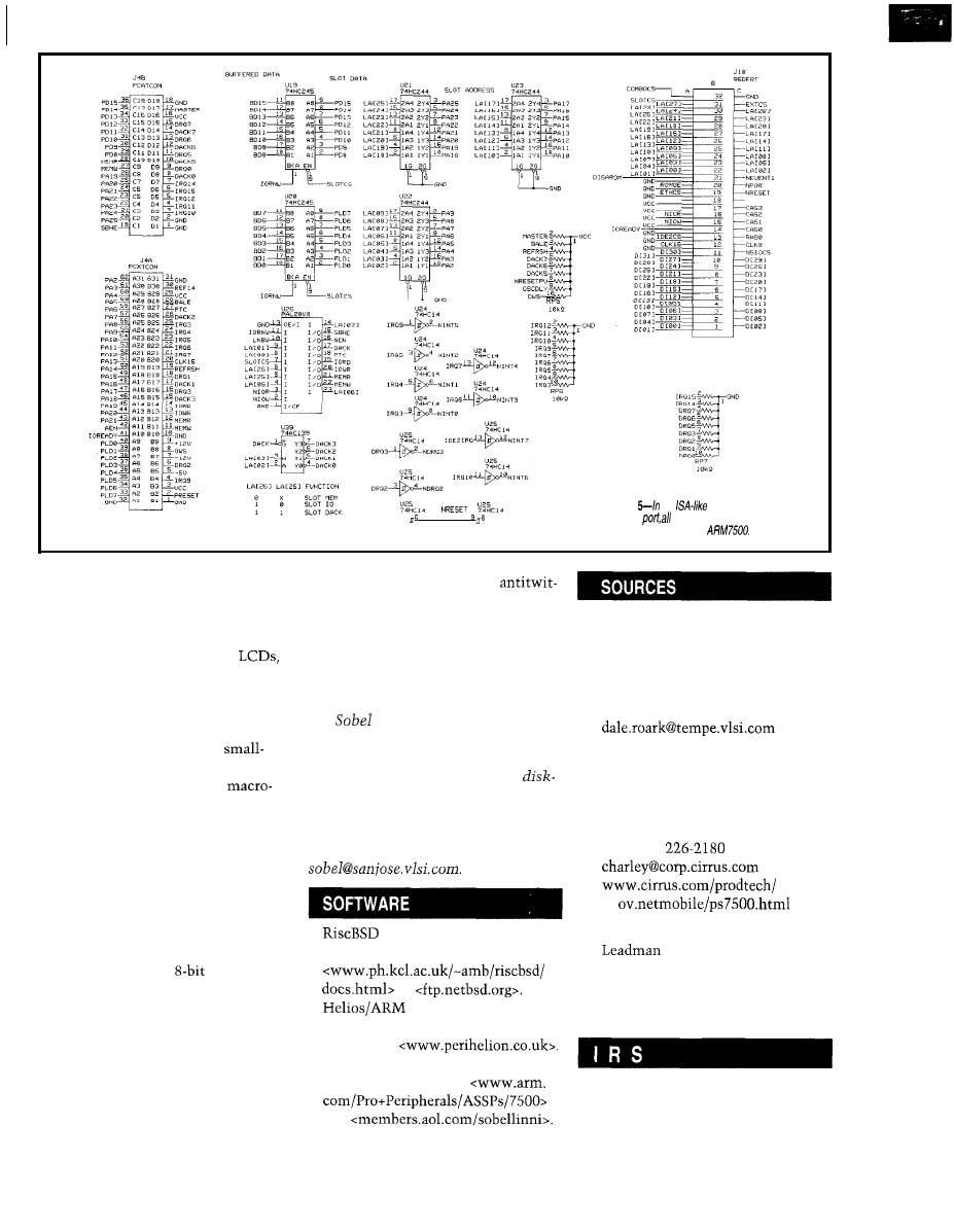
Figure
the
expansion and logic
RESET
l
PRESET
analyzer
of the expansion signals are
buffered to protect the
systems are supported, high-perfor-
mance 32-bit or lower-cost 16-bit sys-
tems can be designed.
The ARM7500 drives monochrome
(single or dual panel) and color
which is useful for electronic instru-
ment displays. The ARM7500 has been
designed into marine and aircraft GPS
and is presently being used in a cockpit
display system that makes a
aircraft panel resemble a 747’s.
The combination of ARM
cell processing power and peripheral
macrocells enable the chip to fit into
any application requiring high-quality
video, sound, and general data I/O
(e.g., laser karaoke and DVD players).
Its good performance, low cost, and
integration make it an economical
solution for the sub $500 Web termi-
nals. It can also be embedded in TVs,
replacing the simple
micro that
handles the IR receiver to switch chan-
nels and adjust volume.
As a display device, TV currently
suffers from low-bandwidth video
amplifiers and interlaced scan. It loses
display detail and has an annoying
flicker in high-contrast fonts and line
drawings. To compensate, high-detail
areas must be antialiased and
tered (i.e., the frames must blend into
each other to reduce contrast).
In Part 2, I’ll discuss programming
the ARM7500 in the RC7500 board.
I’ll also take at look at the Demon
ROM and console test program.
q
Art
is the hardware applications
manager for embedded products at
VLSI Technology. He has spent 24
years in Silicon Valley designing
drive electronics and controllers, laser
interferometers, laser-printer control-
lers, many controller chips, and speech
synthesizers. You may reach Art at
and GNU cross-develop-
ment software is downloadable from
or
A
RTOS package is avail-
able from Perihelion Distributed
Software at
More information on ARM7500 and
boards can be found at
and
ARM7500 chips and RC7500
development board
VLSI Technology
1109 McKay Dr.
San Jose, CA 95 13 1
(602) 752-8574
ARM7500
Cirrus Logic, Inc.
3100 W. Warren Ave.
Fremont, CA 94538
(510) 623-8300
Fax: (510)
ARM7500 case
Electronics
2980 Gordon Ave.
Santa Clara, CA 95051
(408) 738-1751
410
Very Useful
411 Moderately Useful
412 Not Useful
Circuit Cellar INK@
Issue 82 May 1997
5
1
Brad Stewart
0
our bits rule!
Billions of 4-bit
Here’s a short list: toasters, cam-
eras, watches, exercise equipment,
smart batteries, calculators (including
graphing and scientific), battery charg-
ers, bread makers, coffee makers, wash-
ing machines, and weather gauges.
microprocessors are in
use today in all kinds of
applications.
According to market research, the
number of 4-banger
(over a bil-
lion) shipped worldwide in 1996 ac-
counts for nearly 32% of all units sold.
That’s over four times the number of
MCU units sold. (For the record,
54% of MCU units sold are 8 bit.)
Oh, and then there are vacuum
cleaners, garage-door openers, ovens,
thermostats, hand-held games, sprin-
kler controls, water softeners, fishing
lures, automotive systems, telephones,
organizers, portable stereos, and remote
controllers, not to mention
meters and test instruments.
By far, the largest suppliers of 4-bit
are Japanese and Korean compa-
nies like NEC, Sharp,
Toshiba,
and S-MOS. Sharp has dozens of mod-
els and variants of their 4-bit micros,
each targeted for specific markets.
You may think that a 4-bit micro is
outdated, old fashioned, and even retro.
So, why are they still used in such large
numbers? And, why should you use a
nibble nosher when there are so many
or
to choose from?
There are many reasons, of course,
but consider these. These little guys
have been around a long time-over 25
years. Remember the
For example, the Sharp
has
a 3
LCD graphics driver, 8 KB
of SRAM, half a megabit of ROM, wide
supply voltage, and
standby cur-
rent. In addition, the LCD driver signals
are multiplexed to scan a keyboard and
access up to 16 MB of ROM.
They’re cheap. These
are
often around $1 in high quantity. And,
they consume very little power, often
only microamps. Some versions can
even run on 1.5 V.
This part is designed specifically for
electronic portable hand-held organiz-
ers, language translators, dictionaries,
and Bibles.
Four-bit
come in many pack-
age sizes and form factors, including
bare die which can be bonded directly
to a circuit board or a thin flex film.
Lower circuit complexity allows for
larger chip geometries which results in
an integrated circuit that is rugged and
less susceptible to static discharge and
high-voltage electromagnetic fields.
UNDER THE HOOD
Lower power means lower levels of
EM1 emissions making them easier to
FCC certify.
Let’s look at one of these nibble
crushers in more detail. Figure 1 shows
a block diagram of the
manu-
factured by Sharp Electronics.
These devices are feature rich and
include useful peripheral circuits such
as LCD and vacuum fluorescent display
drivers, timers, counters,
and
power management, real-time
clocks, LED drivers, I/O, serial ports,
sound generators, and interrupts.
This
parallel processor has 52
instructions, 4 KB of ROM, 256 nibbles
of RAM, and an 8-channel
ADC.
It has 8 direct-drive LED outputs,
power standby mode, two counters
with
prescaler (use one as a
watchdog timer), synchronous serial
port, 3 internal and 2 external inter-
rupts, 4 inputs, and 20 input/outputs.
Fast. Yes, you read it right! It’s not
It runs on a 2.0-5.5-V supply and is
uncommon to find turbo fours with a
available in a 36-pin QFP or 30-pin
instruction time. Adding to the
computational efficiency is that most
instructions are executed in one cycle.
Hey, that’s around a MIPS!
So where do these little jewels pop
up? More places than you might think.
52
Issue 02 May
1997
Circuit Cellar INK@
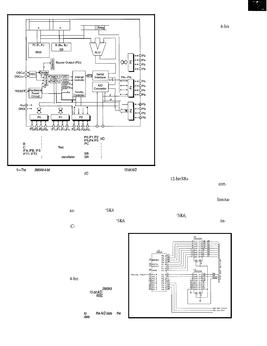
ROM
RAM
4096 8 bits
256 4 bits
Areg
c
I
l l
VRAGND
LEGENDS
Areg
A register (Accumulator)
ALU
Arithmetic Logic Unit
Program counter
Carrv latch
RAM
Data memory
: Interrupt request flag
o s c ’
System clock
ROM
Xreg
Program memory
SB register (Stack B-reg)
Stack register (Stack PC)
: X register (Sub accumulator)
Figure
Sharp
microcontroller is a complete system on a chip featuring a
converter,
dual timer/counters, a serial interface, and 20 programmable pins.
SDIP package. For prototyping and
small production runs, the part is av-
ailable as an OTP (one-time program-
mable) version.
Code development is done using a
PC-based assembler/linker and an
circuit simulator. One of the more
“modern” enhancements to 4-bit de-
velopment is the introduction of a
like structured assembler, which I
discuss in more detail later on.
PROGRAMMING MODEL
My first exposure to a 4-bit micro
was at college. It was briefly men-
tioned in our digital logic class but was
dismissed as obsolete because, by then,
Intel had announced the 8008.
Then, just this year, I looked at
micros a bit more seriously and with
renewed interest and curiosity while
attempting to dismiss the “wimp”
label some were trying to attach to
4 bits (or was it me?).
“How is it possible?” I asked my-
self. “How do you get 52 instructions
and 4 KB of address space with only
The X register is a 4-bit register that
holds temporary data. The A and X
registers can combine to form an
value.
A 4-bit ALU performs parallel op-
erations. For example, the ADC in-
struction does a binary addition with a
nibble value stored in RAM, the A
register, and the carry bit. The result
is placed in the A register, and the
carry bit is generated if a carry occurs
during ALU operation.
The B register is an 8-bit register
that specifies the RAM address. The
upper 4 bits is called the BM register,
and the lower bits is the BL register.
In addition, the B register can be
used as a general-purpose register. It
can also hold the address of internal
control registers during the execution
of input, output, and test instructions.
There is also an 8-bit SB register
that’s used as a save register for the B
register. The contents of B and SB can
be exchanged using the
E X
instruction.
The PC (program counter) is 12 bits
wide and specifies the ROM address.
The upper 6 bits [one nibble plus one
crumb) represents one of 64 pages, and
the lower 6 bits denotes one of 64
steps in a page. There is also a set of
eight
(stack registers).
During a subroutine call, the
4 bits? How can you do anything with
tents of the PC are pushed onto the
4 bits?”
stack, allowing for up to eight levels of
Well, it works a lot like an 8-bit
subroutine nesting. It’s a slight
micro-but different. And, you’ll soon
tion, I agree, but it’s better than many
see that the
is anything but a
8-bit micros.
wimp. Let me start by explaining the
In the
there are 4 KB of ROM
register set of the
for program and data storage. All
The A register, or accumulator, is a
structions are one byte and operate in
4-bit general-purpose
register. It is used
with the ALU, C
(carry) bit, RAM, and
transfers data be-
tween input and
output terminals.
Figure
2-The
is used
as a
converter for
the ARM
micropro-
cessor. The optional S/O
provides extended capabili-
ties. The bus controller
provides a chip-select signal
strobe
on
bus.
Circuit Cellar INK@
Issue 82
May
1997
53
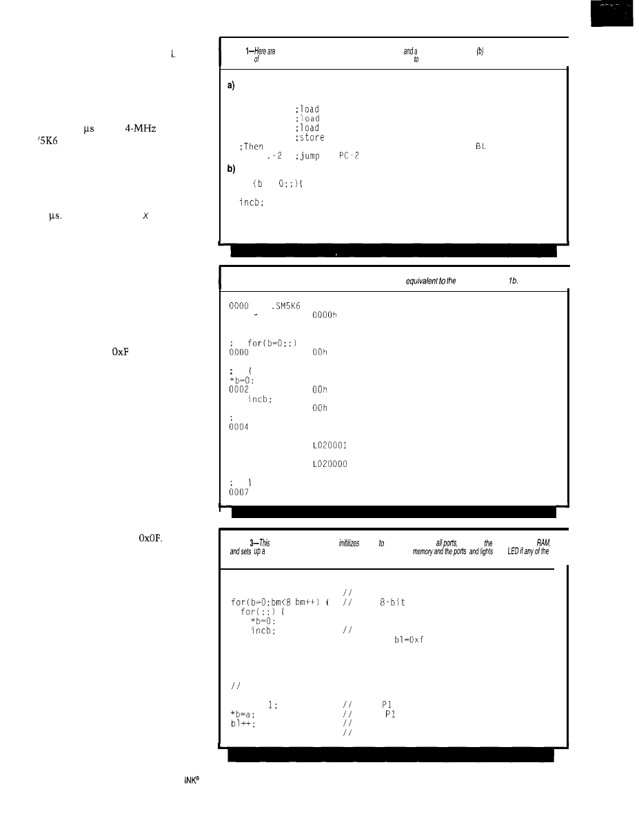
one cycle, with the exception of
CALL,
DR (clears the clock dividers),
T
(trans-
fer over page boundaries), and PAT
(table look-up), which require two bytes
and two cycles.
Therefore, 90% of the instructions
are one byte and are executed in one
cycle, or 1 with a
clock. (The
divides the input clock by four.)
Now that you know the basics,
here’s some code. Listing la sets the
first 16 nibbles of RAM to 0.
The code in Listing
la
requires
5 bytes of ROM and executes in about
34 Notice the
EXC D
instruction
(Exchange Contents of RAM with
accumulator and decrement BL). It
does many things at once.
First, it performs an exclusive OR of
the contents of the BM register with
the crumb (2 bit) value x, leaving the
result in the lower crumb of the BM
register. After the instruction is ex-
ecuted, the instruction that follows
E X C D
is skipped if the contents of BL
register becomes
as a result of a
carry.
Using the x value makes it easy to
set up the B register, say, for example,
when you want to copy or move the
contents of RAM to another location
across page boundaries. In this case, I
set x to 0 so that BM remains 0.
The assembler supports some macro
instructions. For example, you can
replace the first two instructions with:
Listing
examples ofhowan assembler routine (a)
C-like routine clear the first 16
nibbles RAM. As
you
can see, fhe C-like routine is easier follow.
1
MCLR:
LBMX OH
BM to zero
LBLX OFH
BL to zero
LAX OH
accumulator with zero
EXCD OH
contents of A into RAM address B
decrement BL and skip next instruction if = 0
TR
to
for =
*b = 0;
//set contents of address in b to 0
//increment BL and skip next instruction if 0
continue:
break:
Listing 2-A C-like compiler generates an assembly listing
routine in Listing
I
0000
ORG
LBL
0002 1020000:
LAX
6 0 0 3
EXCI
continue;
TR
b r e a k :
0005 TR
0006 LO20002
0006 TR
0007 1020001
END
//clear first 16 nibbles of RAM
//increment bl and skip next instruction if 0
LO20002
LBL OFH
which loads the entire B (all 8 bits)
register with the value
It still
assembles into two l-byte instructions.
C-LIKE STRUCTURED ASSEMBLER
One of the more innovative en-
hancements to 4-bit tool design is the
introduction of a C-like structured
assembler. It is not a true C compiler,
but it does look and feel like C code
with the added benefit of making it
easier to write and read your code.
It also takes care of the overhead of
program transfers across page bound-
aries. For example, Listing la could be
written as Listing lb.
The C-like compiler generates a
source listing (see Listing 2) where the
C-like code is commented out and it
Listing
C-like structured assember
RAM zero, reads
saves values in
timer interrupt. The timer interruptpolls
an
ports or memory has changed.
I
Initialize:
org 0;
continue
break;
clear all 128 nibbles of RAM
b is
register, bm is 4 bit
increments bl reg, skips next inst
if
read all ports and store in first five memory locations
bm=O;
inp
read
store data to RAM
increment RAM address
inp
2:
read P2
(continued)
54
Issue
82 May 1997
Circuit Cellar
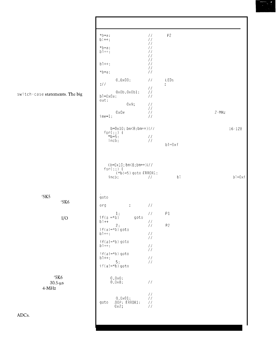
generates the appropriate assembly
instructions. At this point, you can
hand optimize the code then assemble
it as you would a “normal” assembly
source listing.
Note that the C-like program re-
quires 7 bytes instead of 5. However,
as code increases in size and complex-
ity, the difference in the program size
is minimal, especially after some hand
optimization.
In some cases, the C-like compiler
can produce more efficient code, espe-
cially when working with pointers and
plus, though, is that C-like code is
much easier to read and debug, as the
next example illustrates.
REAL-WORLD TEST EXAMPLE
When you use a microcontroller in
many HVAC applications, the device
is susceptible to some pretty harsh
environments. Before a part can be used
in a gas ignitor, for example, it must be
subjected to a number of brutal tests
including the “shower of sparks.”
This test entails placing a Franken-
stein-like spark-gap generator in close
proximity to the micro while it runs a
test program. Your job: hope and pray
it doesn’t fry.
Listing 3 is C-like test program
written for a
microcontroller. (It’s
basically the same as a
but has
128 nibbles of RAM and 2 KB of ROM.)
It sets up an interrupt that occurs
every 10 ms to read the
ports and
scans RAM for any changes that might
have occurred between interrupts. If
anything has changed, an appropriate
LED is activated.
Originally, this code is written
entirely in assembly. When converted
to structured C-like assembler, the
code size differed by only two bytes.
OTHER APPLICATIONS
The ADC on the
has
10
bits of
resolution with a
conversion
time (using a
clock). When you
consider that this part costs close to a
buck (for a masked version in large
quantities), you have an economical
replacement for many standard lo-bit
But since it’s a microcontroller, you
could add some enhancements such as
56
Issue
82 May 1997
Circuit Cellar INK@
Listing 3-continued
store data to RAM
increment RAM address
inp
3;
read P3
store P3 data to RAM
increment RAM address
inp
4:
read P4
*b=a;
store P4 data to RAM
increment RAM address
inp
5;
read P5
store P5 data to RAM
outp
turn
off
timer initialize routine
dr;
divider clear
outp
modulo register set
timer counter set
outp
oxoc
outp
LOOP
for
timer mode control register set
divide input clock by 128
0x4;
interrupts every 10 ms with
clock
interrupt enable
write bit pattern to locations
use 0101 bit pattern
increments bl register, skips next inst
if
continue
break:
for
read RAM and check that it did not change
if
increments reg, skips next inst if
continue
break:
LOOP;
0x0204
bm=O
inp
ERROR
inp
ERROR:
inp
3;
ERROR:
inp
4:
ERROR:
inp
ERROR:
//set ok LED
outp
outp
rtni;
ERROR:
outp
E
outp 0
ELOOP:
got0
ELOOP:
TSR from timer interrupt
read
increment RAM address
read
increment RAM address
read P3
increment RAM address
read P4
i n c r e m e n t R A M a d d r e s s
read P5
pulse LED measure it with oscilloscope
this is port read error
light port error LED
memory error
light RAM error LED
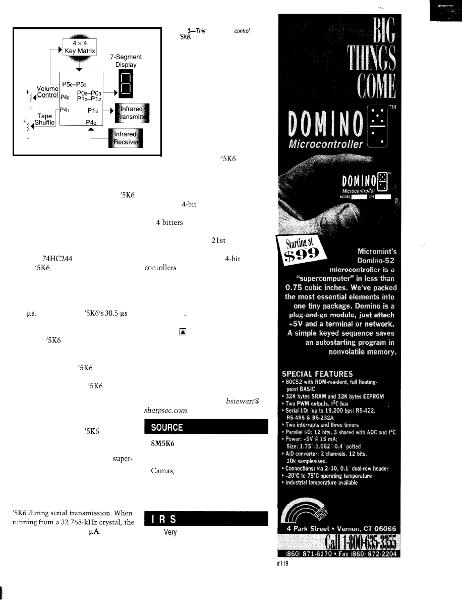
automatic gain control, a VOX switch,
compression, or some simple digital
filtering.
Figure 2 shows a schematic of a
used as an speech-sampling circuit
that interfaces to a Sharp LH77790
ARM-based RISC microcontroller. In
this case, the ARM memory-manage-
ment unit uses one of its six chip
selects to read the A/D values via a
couple of
buffers.
The
continuously runs the
ADC at full speed and places the result
on 10 output pins. The ARM processor
reads the port at the desired sample
rate, which for speech is typically
125
well under the
conversion time.
The bidirectional synchronous serial
port of the
could also be used as a
means to transfer commands and data
to and from the host microcomputer.
Being CMOS, the
can be shut
down entirely or run at a slow clock
speed. For example, the
can be
part of a hand-held instrument that
operates as a smart peripheral for a
more advanced microcontroller, such
as an ARM or H Series RISC processor.
In this example, the
performs
several functions. It can serve as a
lithium-ion battery charger, power
management, a real-time clock,
visory control, a low-speed ADC, and
nonvolatile storage.
Communication to the host micro-
controller is via the serial port that is
clocked by the host and interrupts the
Figure
VCR remote
uses
the
threshold, some immediate
action can take place.
And finally, Figure 3 shows
how you might use the part as
an infrared transmitter with
an LED display and keyboard.
In this case, the
is placed
in the Stop mode until a key is pressed
that wakes up the processor.
STILL IN BUSINESS
Yes,
the
microcontroller is here
to stay. Although the market share of
the
is expected to steadily
decline over the years, it will remain
with us well into the
century.
Sharp and other manufacturers are
committed to supporting
micro-
until nobody wants them
anymore. But, that scenario seems
unlikely-a least for a while. In fact,
Sharp is planning new parts that are
even faster, cheaper, and better.
Hmmm.. Maybe if I connect eight
of them in parallel, I could run Unix in
my watch.
Brad Stewart is a senior applications
engineer at Sharp Electronics. He has
over 20 years’ experience in analog
and digital design engineering and
application support, as well as in
marketing and sales. You may reach
Brad at (360) 834-8930 or
Sharp Electronics Corp.
5700 NW Pacific Rim Blvd., Ste. 20
WA 98607
(360) 834-2500
Fax: (360) 8348903
www.sharpmeg.com
part consumes about 20
The ADC
413
Useful
is set to compare mode so that if the
414
Moderately Useful
voltage drops below a programmed
415
Not Useful
Circuit Cellar INK@
Issue 82 May 1997
57
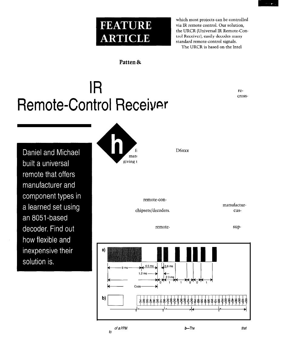
8051 microprocessor. Although it has a
Daniel
Michael Miller
microprocessor, you can successfully
integrate the URCR into most designs
without any microprocessor or pro-
gramming experience.
A Universal
STANDARDS
Our first projects destined for
mote control were an electronic
over and preamplifier. But, we wanted
V I
to use remote control in many differ-
ent projects. The time had come for
ave you ever
finished the ulti-
mate project and after
giving the big demo to
your neighbor, he asks, “Where’s the
remote control?” You soon realize that
part of you agrees. Remote control
would be nice. So, you shift all other
projects to the bottom of the to-do pile.
trol research, you find that there are no
IR standard receiver
You’re not alone. A lot of people have
Unfortunately, not long after start-
ing down that road of IR
had this experience.
In this article, we explain IR
control basics and define a system in
some serious research.
We disassembled every available
remote control (-20 total) and found
that the majority used an NEC trans-
mitter/keyboard encoder chip. The
most widely used chips came from the
series (e.g., the D6124, D6120,
D6122, and D6600).
companies and allocates
ers a unique ID, known as the
tomer code, which is included in the
serial datastream.
NEC makes several different series
of remote-control encoders but no
Most of the tested remotes
decoders. Apparently, most manufac-
ported the NEC standard. And, since
turers have to write code for a micro-
processor in each product they make.
While it may not be a standard,
NEC recommends a particular format
for the serial datastream. NEC registers
13.5 ms
Leader
Leader Code Customer Code Customer Code
Data Code
Data Code
Inverted
Inverted
Figure
1 --The NEC-style
data
format uses a pulse-position-modulation scheme to encode the data.
a-Jhe
interpretation
code is based on the time between pulses.
data
bits marked with *denote bits
are used calculate check sums. This error checking helps ensure that fhe data is decoded correct/y.
58
Issue 82
May 1997
Circuit Cellar INK@
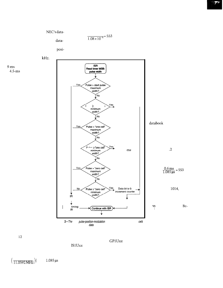
this standard uses a fixed number of
bits in the serial stream and we had
the databook, we decided to use it.
We found that the measured data
correlated very closely to
book figures. Figure la illustrates the
header (i.e., beginning) of the IR
stream.
The NEC standard uses pulse
tion modulation (PPM) with a data
carrier frequency of 38
The header is composed of a
high pulse followed by
a
low pulse. In addi-
tion, a 32-bit datastream
follows the header with no
end-of-header or stop bits.
If the gap between pulses forming a
0 in the IR serial datastream is 0.6 ms,
the 805 1 can run -553 instructions
while waiting for the next pulse:
0 . 0 0 0 6
Even with the most bloated code, an
805 1 should have enough horsepower
to decode the serial datastream.
in gated mode and the interrupt in
edge mode.
We used this method because a
timer will run (count) as long as the
interrupt pin is deasserted. That is, the
timer counts the gaps between pulses,
and the code is interrupted at the start
of every high pulse.
This way, on each interrupt, an ISR
(Interrupt Service Routine) can deter-
mine whether a long or short
gap has occurred, reset the
counter, and wait for the
next interrupt.
PPM might appear confus-
ing at first, but it’s relatively
straightforward. Look at the
gaps between data pulses. A
long gap represents a data
value of 1, and a short gap
represents 0.
Pulse start pulse
Start Pulse:
reset counters
Figure lb illustrates the
signal composition. Of the 32
data bits, only 16 carry com-
mand information. The other
16 are for error checking.
This high level of data
redundancy, if the decoder
takes advantage of it, can
result in a high degree of
accuracy in decoding trans-
mitted commands. We knew
what the IR transmitter was
sending. We just had to de-
code it!
Pulse
Data bit is 1
increment
MICROPROCESSOR
IMPLEMENTATION
Our first decision: Which
microprocessor to use? We
were familiar with the Intel
805 1, so we went with that.
How much horsepower? Not
very much, as a few quick
calculations show.
pulse
and byte counters
Reset
Invalid
clear data
Check for end of byte
and end of command
A standard clock fre-
quency for an 8051 is
Figure
basic
decoding algorithm uses time
to determine the value of each
bit.
zero). This timer/counter is
implemented with a low and high
byte. The low byte of the timer can
count to 256, and the high byte of the
timer is only incremented every time
the low-byte timer reaches 256.
To accommodate different
types of remotes, we created
a one cell and a zero cell. A
cell is a time measurement
the 805 1 uses to determine if
data is a 1 or a 0 If a pulse is
of a width that falls in the
one cell, the data is inter-
preted as a 1.
The 8051’s timer incre-
ments every 1.085 us. The
indicates that the
zero gap should ideally be
0.6 ms. A O.l-ms margin
accommodates timing errors,
resulting in a cell of 0.5-0.7
ms. For a one gap, the cell
margin is
l-l
ms.
For an ideal zero gap, the
counter increments 553
times:
11.0592 MHz, with the microprocessor
taking clock cycles to complete a
standard instruction. Therefore, an
805 1 executes an instruction about
every microsecond (nearly 1 MIPS!):
1
12) =
HARDWARE
Our receiver of choice-the Sharp
IR module-is part of the
and
families. It’s the perfect match
for the 805 1.
To set up the hardware, we con-
In trying to keep the code easy, we
nected the IR module to an 805 1 inter-
ignore what the low byte of the timer
rupt pin and put the associated timer
is doing. This way, we only have to
The count margin is 461-645
times. For a one gap, the
ideal count is
and the
margin ranges from 922 to
1106.
These count results are
di ‘ded by 256. Why?
cause the 805 1 timer has
16-bit resolution (i.e., it can
increment 65,536 times
before wrapping back to
Circuit Cellar INK@
issue 92 May 1997
59
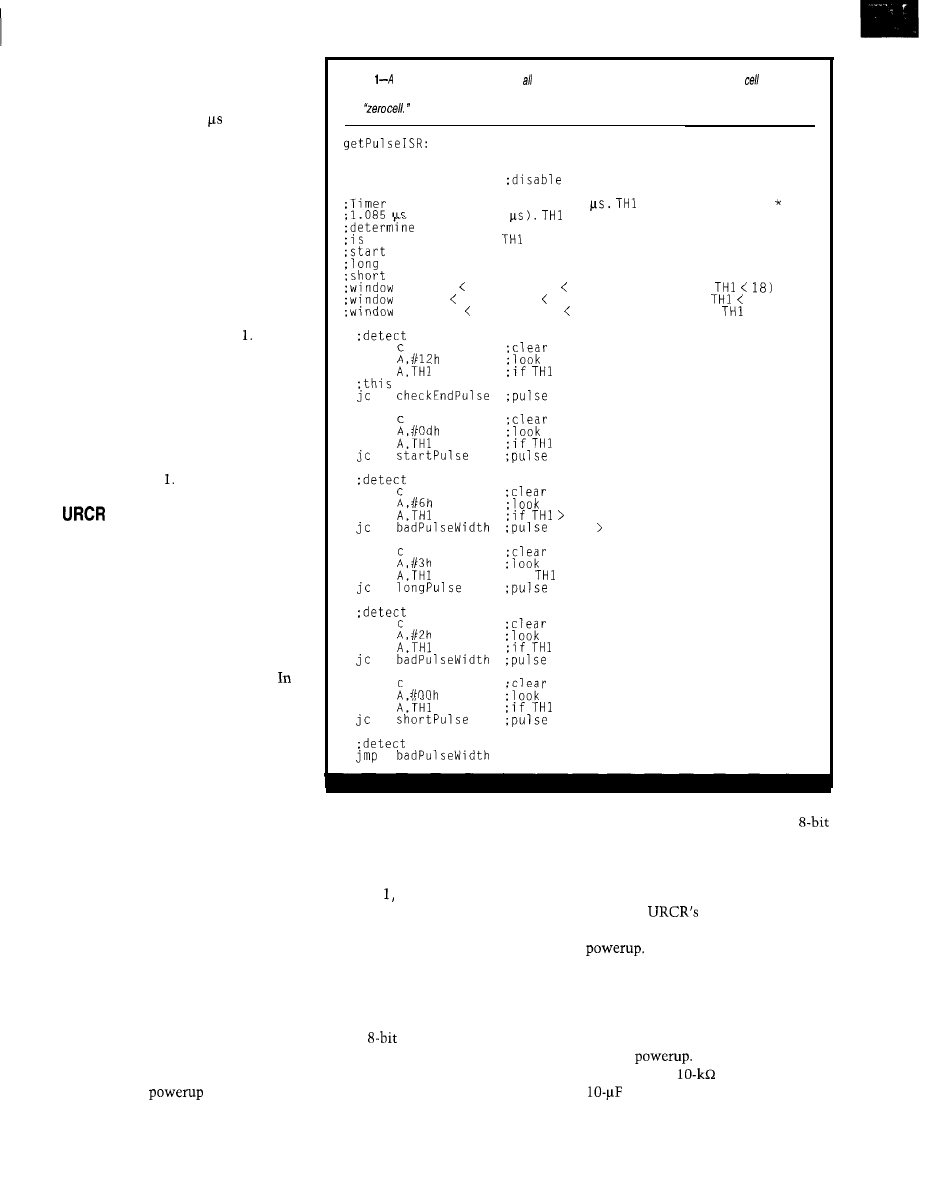
compare one byte (the high byte) to see
if a gap is a zero or a one.
The high byte provides enough
resolution (256 x 1.085 = 277.8 us)
for this application. In practice, this
technique works quite well.
A zero gap is represented by the
high-byte timer being either a 1, 2, or
3. A one gap is represented by either a
4, 5, or 6.
FIRMWARE
We wrote the code for the 8051 in
assembly. Figure 2 is a flowchart for
the cell-detection algorithm we imple-
mented in an ISR for the 805
Each time an IR pulse is presented
at the interrupt pin of the 8051, the
processor executes this routine to
determine what serial data is being
transmitted.
A corresponding code fragment of
the zero- or one-cell selection is pro-
vided in Listing
By adding a small nonvolatile mem-
ory and writing some more involved
code, we believe we came up with a
novel solution. The URCR is an inex-
pensive and easy way to add IR remote
control to an existing design.
We designed it with a high degree of
flexibility for operation in systems
with or without a microprocessor.
fact, you can easily use it without
knowing that the URCR is really a
microprocessor.
Our goals were to:
l
design a stand-alone microprocessor
for use as a generic IR remote-con-
trol decoder
l
make the decoder easy to paste into
any design
l
make the decoder inexpensive
l
design multiple capabilities so the
decoder can match any target sys-
tem’s capabilities
l
make the decoder learning, so it can
accommodate most remotes
To achieve the flexibility for imple-
mentation in a variety of systems, the
URCR has six operation modes. They
are pin programmed on the micropro-
cessor, which puts itself into one of
the modes on
(see Table 1).
Listing
few simple checks of the timer are that is needed to determine info which the data bit
should be categorized. Erroneous data is detected when the bit does not match the definition of a “one cell”
or a
push PSW
push ACC
clr EA
interrupts
is incremented every 1.085
resolution is 256
(i.e., 277.8
value should be close enough to
start pulse width. Start pulse width is 4.5 ms, which
4147 timer ticks.
would have been hit 16 times.
pulse = 4.5 ms
pulse = 1.58 ms
pulse = 0.46 ms
= 3.889 start pulse 5.0 ms (i.e., 14 <
is 1.1 long pulse 1.667 ms (i.e.,
4 <
6)
is 0.277 short pulse 0.833 ms (i.e., 1 <
< 3)
start pulse
clr
carry bit for comparison
mov
subb
at timer high byte
> 18, set CF
could be the end pulse! check for it!
width > threshold
clr
carry bit for comparison
mov
subb
at timer high byte
> 14, set CF
is a start pulse
long pulse
clr
carry bit for comparison
mov
subb
at timer high byte
6. set CF
width threshold
clr
carry bit for comparison
mov
subb
at timer high byte
;if
> 4, set CF
is a long pulse
short pulse
clr
carry bit for comparison
mov
subb
at timer high byte
> 3. set CF
width > threshold
clr
mov
subb
carry bit for comparison
at timer high byte
> 1, set CF
is a short pulse
glitch pulse
MORE HARDWARE
As Figure 3 shows, the URCR
doesn’t need many extra components
to run. Basic hardware is sufficient for
Modes 0, and 2.
code can also be in the form of an
latch loaded by another microproces-
sor.
The five required component sec-
tions are customer-code input, reset
circuit, mode selection, IR receiver,
and oscillator circuit. Other optional
connections can be added for increased
functionality.
Connecting three switches to pins
MODEO-MODE2 provides a way to
select the
operating mode.
The switch positions are only valid at
The URCR system ignores
subsequent changes in their values.
The switch positions are shown in
Table 2.
Recall that the NEC standard speci-
For the 805 1 microprocessor to start
fies an
customer code. This code
properly, the Reset pin must be held
is fed into the URCR by attaching
high at
This task is accom-
eight switches (a DIP switch can be
plished by the
resistor and
used) to pins CCO-CC7. The customer
capacitor.
60
Issue
02 May 1997
Circuit Cellar INK@
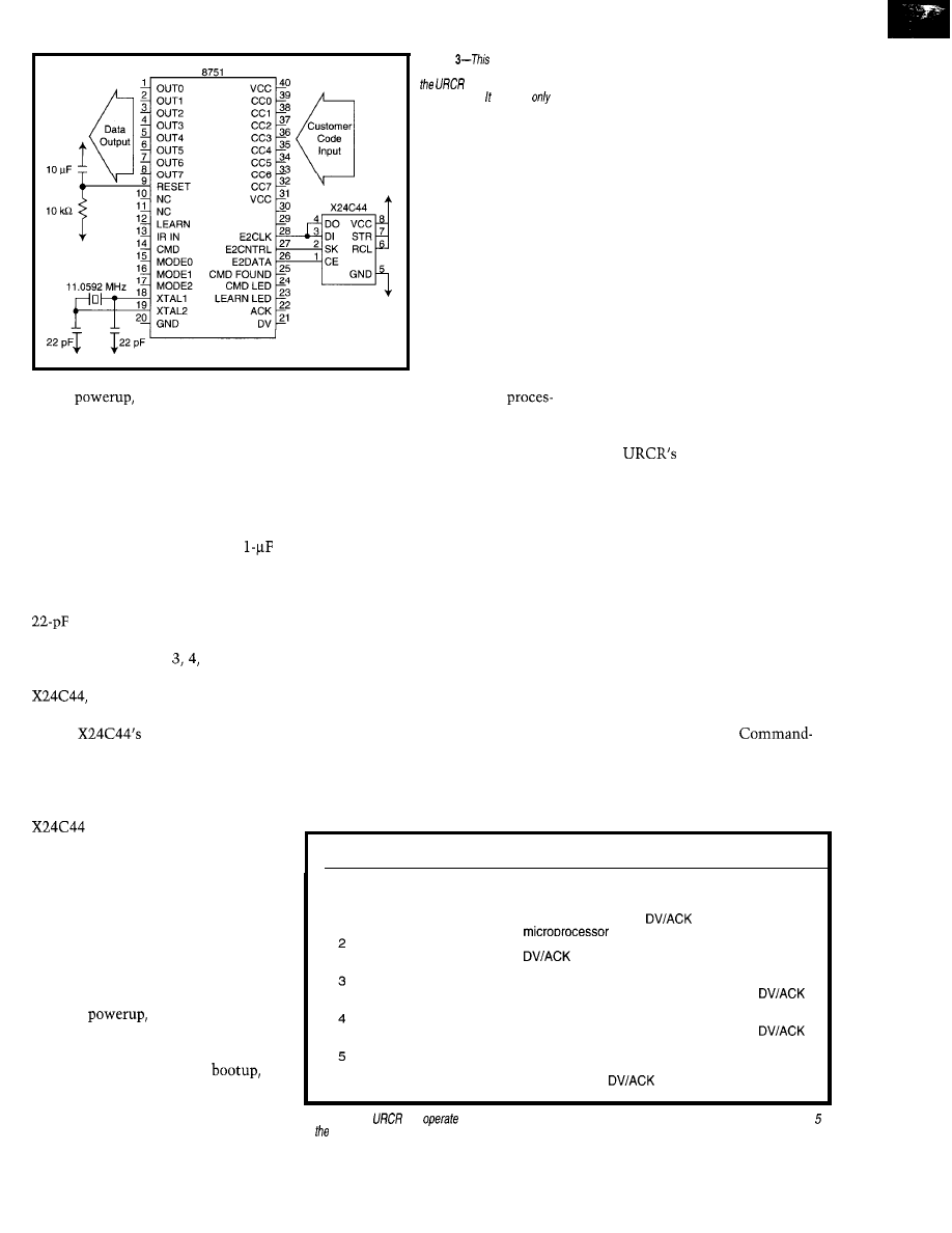
Figure
simple
schematic shows how easily
system can be
implemented. requires
six external components.
On
the capacitor charges
Once the switch is read, the
and acts as a low-resistance connection
to the 5-V supply. When the capacitor
is done charging, it acts as an open
The IR receiver’s output is con-
nected to pin 13 of the microprocessor.
The receiver can be somewhat suscep-
circuit to the 5-V supply.
tible to power-supply noise, so a
tantalum capacitor connected directly
across its power pins is advised.
The
11.0592MHz
crystal and two
capacitors form an oscillator for
microprocessor operation.
To support Modes
and 5, you
need an EEPROM. We used a Xicor
which can store 256 bits of
nonvolatile information.
The
memory is organized
as a 16 x 16 matrix. Since 16 com-
mands can be stored, there can be
8 bits of command and 8 bits of cus-
tomer code for each command. The
has a very simple interface
and only requires three connections to
the microprocessor.
sor calls the appropriate run-time rou-
tine. The processor remains in the
In the most basic operating modes,
the processor may only poll status bits
operating-mode routine until power is
to see if a new command was received
and export the command data. In more
turned off.
complex modes, the microprocessor
polls for new commands, searches the
EEPROM to match incoming com-
mands to learned ones, monitors the
Learn and Command buttons to arbi-
trate the command-learning process,
stores new commands to EEPROM,
and exports valid command data with
a Data Valid/Acknowledge protocol.
The processor enters the ISR when
the interrupt line is asserted by an IR
pulse. The timer is gated off during ISR
execution, and it is reset and gated on
at
the end of the ISR. This way, the
8051 can measure the time between
pulses and determine the data value
encoded via a PPM scheme.
In addition to the PPM decoding,
the ISR is responsible for grouping the
pulses into bytes, calculating check-
sums to verify data integrity, and up-
dating the new command flag to alert
the operating loop that a new com-
mand was received.
In the operating-mode loop, the
processor monitors the new command
flag indicating that a new IR command
was successfully received and pro-
cessed by the ISR. Once the processor
knows it has new data to act on, it
exports the data as required for each
operating mode. For learning modes,
arbitrating the command-learning
process is also performed in this loop.
The
learning capabilities
provide a powerful tool for implement-
ing custom IR designs. The flexibility
of using any universal remote control
to dynamically program the URCR
makes its programming simple. Figure
4 outlines the learning process.
You enter the learning mode by
pressing the Learn button, and the
Learn LED is activated. Once in the
loop, a second Learn button press
causes the processor to leave this mode.
Therefore, pressing the Learn button
twice in a row erases the command
memory.
In the learning loop, a
button press puts the processor in the
command-button loop. The Command
LED lights to identify this mode.
Mode Description
Notes
CODE FUNCTIONALITY
The URCR code comprises five
major components-initialization, the
pulse ISR, the operating-mode loops,
the learning routines, and the EEPROM
search routine.
After
the processor initial-
izes itself and determines its current
operating mode. The operating mode is
read from three switches at
and changes in switch settings do not
affect the processor until power is
cycled.
0
Basic
Commands passed through, Customer code from
switches, Commands are static and replaced by
next command
Microprocessor Interface
Single Byte
Microprocessor interface
Double Byte
Commands available,
handshaking for the
interface
Commands available, Customer code available,
handshaking for the microprocessor
interface
Basic Learning
Microprocessor Interface
Learning Single Byte
Microprocessor Interface
Learning Double Byte
Learning mode supported with addition of serial
interface EEPROM. Commands available.
handshaking for the microprocessor interface
Learning mode supported with addition of serial
interface EEPROM, Commands available,
handshaking for the microprocessor interface
Learning mode supported with addition of serial
interface EEPROM, Commands available, Customer
code available,
handshaking for the
microprocessor interface
Table 1
--The
can
in one of these six modes. Mode 0 is the most basic implementation and Mode
is most involved.
Circuit Cellar INK@
Issue 92 May 1997
61
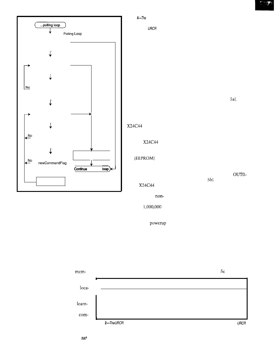
Is Learn button
No
being pressed?
Figure
learning
loop is
controlled by two buttons:
Learn and Cmd. Each button
press steps the
through
this algorithm.
Yes
Learn-Button Loop
Is Learn button
Yes
being pressed?
No
No
Is Command button
being pressed?
Yes
Command-Button Loop
Is Learn button
Yes
being pressed?
No
The URCR then waits for either a
Is Command button
being pressed?
current command is
already learned. If it
is, the URCR ex-
ecutes the appropri-
ate data movement.
Otherwise, it ignores
the command.
The URCR’s
serial
EEPROM stores the
learned-command
set. The
is
divided into volatile
(SRAM) and nonvola-
tile
sec-
tions.
The SRAM pro-
vides unlimited reads
or writes and is used
for all
ac-
cesses except for
storing data to
volatile memory. The EEPROM can
Yes
Store data to EEPROM
nonvolatile memory
I s
set?
in potting
I
Yes
Store
command to
EEPROM
Learn-button press to exit the learning
mode or a new command to be re-
ceived and flagged by the ISR. Addi-
tional Command-button presses have
no effect while the URCR waits for a
new command.
On entering the learning mode, the
EEPROM address pointer is reset to
0x0000 and incremented with each
new command. When the ISR receives
a valid command, the Command LED
turns off and the command is assigned
to the next available EEPROM
withstand a minimum of
store operations.
The EEPROM is accessed to load
the SRAM with valid data at
and to store the learned set of com-
mands. When command data is stored
in the EEPROM, it’s stored with the
most significant byte (i.e., the cus-
tomer code) first.
When a command matches a
learned command, the Command
Found LED flashes to indicate a suc-
cessfully completed memory search.
The URCR’s learning scheme en-
ables the user to mix manufacturers
and component types in the learned
set. For example, if you use the URCR
in an audio system, a power amplifier
can be controlled by the Sony TV codes
and an electronic crossover can be
controlled by the Pioneer CD codes.
MODES OF OPERATION
In Mode 0, the user sets the desired
customer code via switches on micro-
processor pins CCO-CC7. Any com-
mand that matches the customer code
and passes error checking is output on
pins OUTO-OUT7 (see Figure
The command stays on these pins
until another valid command is re-
ceived. In a simple system, devices
(e.g., relays) can be activated on a spe-
cific command and stay active until
another command deselects it.
Mode 1 supports a microprocessor
interface, so a system already with a
microprocessor can easily interface to
the URCR. Customer codes are se-
lected via switches on microprocessor
pins CCO-CC7. Any command that
matches the customer code and passes
error checking is output on pins
OUT7 (see Figure
The command stays on these pins
until the ACK (Acknowledge) pin on
the URCR is asserted low. The URCR
notifies an external microprocessor
that a valid command was received by
asserting the DV (Data Valid) pin low.
A single command stays on pins
OUTO-OUT7, and the URCR ignores
further commands until the external
microprocessor asserts ACK, notifying
the URCR that the command byte was
read.
Mode 2 is nearly the same as Mode
1, except the customer code is also
output on pins OUTO-0UT7. The
customer code is output first, followed
by the command. Figure illustrates
ory location.
The URCR exits the learning mode
if all available EEPROM memory
I
Mode
Mode2
Model
Mode0
Function
tions have been programmed. The
I 0 off
Off
Off
Basic
Learn LED turns off to alert the user
that
the URCR has reached full
ing capacity.
The operating modes that use
1
Off
Off
O n
Microprocessor interface, single byte
2
Off
On
Off
Microprocessor interface, double byte
3
Off
On
On
Basic, learning
4
On
Off
Off
Microprocessor interface, learning, single byte
5
On
Off
On
Microprocessor interface, learning, double byte
mand learning rely on the EEPROM
search routine to determine if the
Table
can be used in one of these six modes. To select a mode, simply set the switches. The
will enter fhe selected mode when power is applied.
62
Issue 82 May 1997
Circuit Cellar
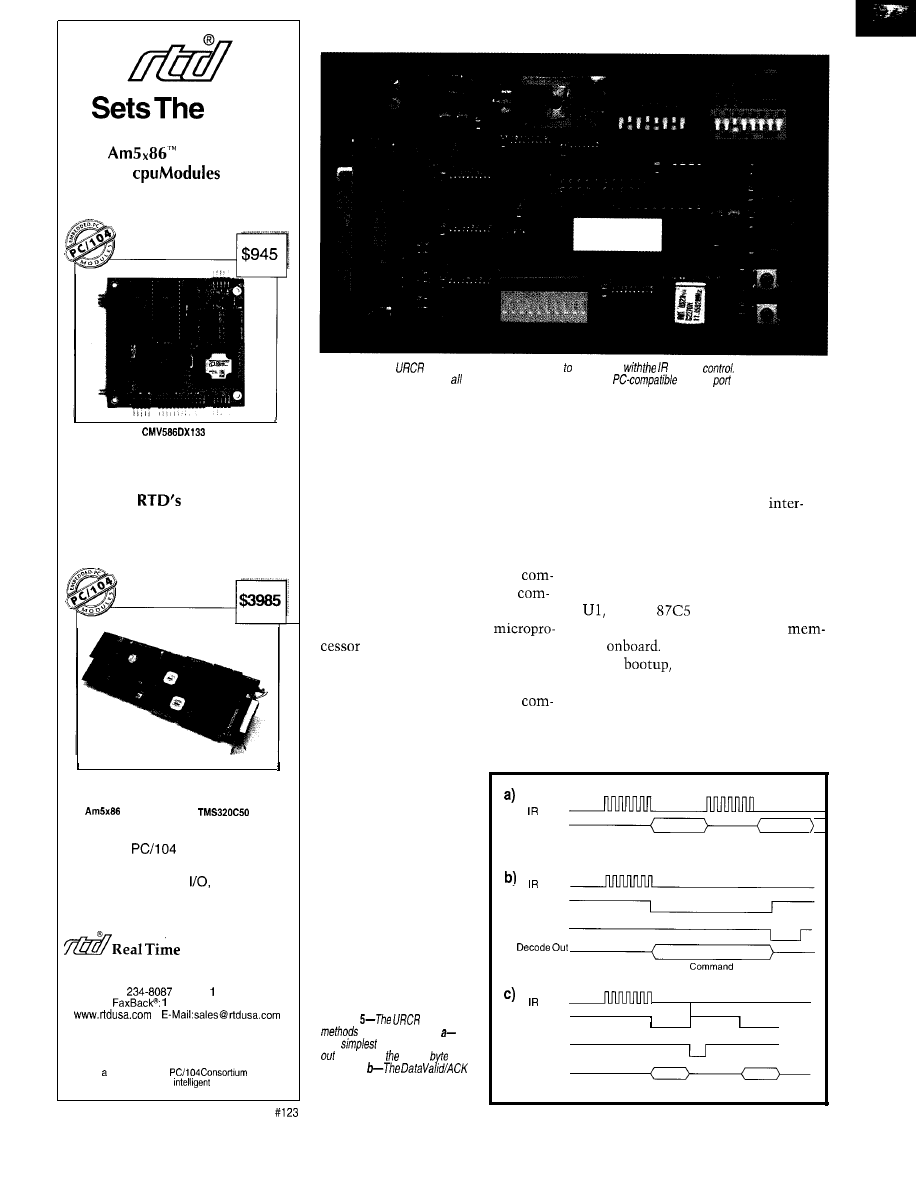
Pace
133 MHz
PC/l 04
Exceed
Pentium-75 Performance
The
offers
versatile embedded functionality
Embedded PC and DSP
Drive
Intelligent
Data Acquisition and
Control Board
The IDAC5210 with PC1104 extension bus,
500 KHz analog and digital front-end
is powered by on-board
133MHz CPU and
DSP
Our
and ISA Bus
product lines feature
Analog and Digital
CPU, DSP,
Shared Memory, SVGA, PCMCIA,
CAN Bus and Intelligent GPS
Devices USA
200
Innovation Boulevard
l
P.O. Box
906
State College,
PA 16804-0906 USA
Tel:
1 (814)
l
Fax:
(814) 234-5218
(814) 235-1260
l
RTD Europa
RTD Scandinavia
Budapest, Hungary
Helsinki, Finland
Fax: 36-1-326-6737
Fax: 356-9-346-4539
RTD
IS
founder of the
and the
world’s leading supplier of
ISA DAS interfaces.
Photo 1
--The
Evaluation Board makes if easy experiment
remote
The evaluation
board is capable of running in six operating modes. If also has a
parallel
interface.
the DV/ACK procedure for reading the
URCR EVALUATION BOARD
two bytes of information.
We developed the multipurpose
Mode 3 incorporates the URCR’s
evaluation board shown in Photo 1 to
learning capabilities. It has the same
explore the URCR’s capabilities. All
data-movement scheme as mode 0, but
functions of the URCR can be tested,
only commands matching the learned
including the microprocessor
commands generate output data.
face, via connection to a personal
In addition, the output data is not
computer through the parallel port.
the IR command. Rather, it’s the
As you see in Figure 6, the URCR
EEPROM address of the learned
eval board supports all six modes of
mand that matches the current
operation. The board is based around
mand.
an Intel
1
microprocessor,
Mode 4 incorporates the
which contains its own program
interface of Mode 1 with the
ory
learning capabilities of Mode 3. Like
On
the microprocessor
Mode 3, the output data is the
reads the status of pins P3.5, P3.6, and
EEPROM address of the learned
P3.7, which are driven by S2.1, S2.2,
mand.
and S2.3. Turning these three switches
Mode 5 combines the data-output
on selects Mode 0.
scheme of Mode 2 with
the learning capabilities
of Mode 3. As with
Mode 2, the output data
Signal
is the learned com-
mand’s customer and
command codes.
Decode Out
Command
Command
Figure
has three
of exporting data.
The
method sends data
as soon as entire
is
received.
scheme can send out one byfe or,
as you can see in (c), two bytes.
Signal
Data Valid
ACK
Signal
Data Valid
ACK
Decode Out
Customer Code
Command
6 4
Issue a2 May 1997
Circuit Cellar INK@
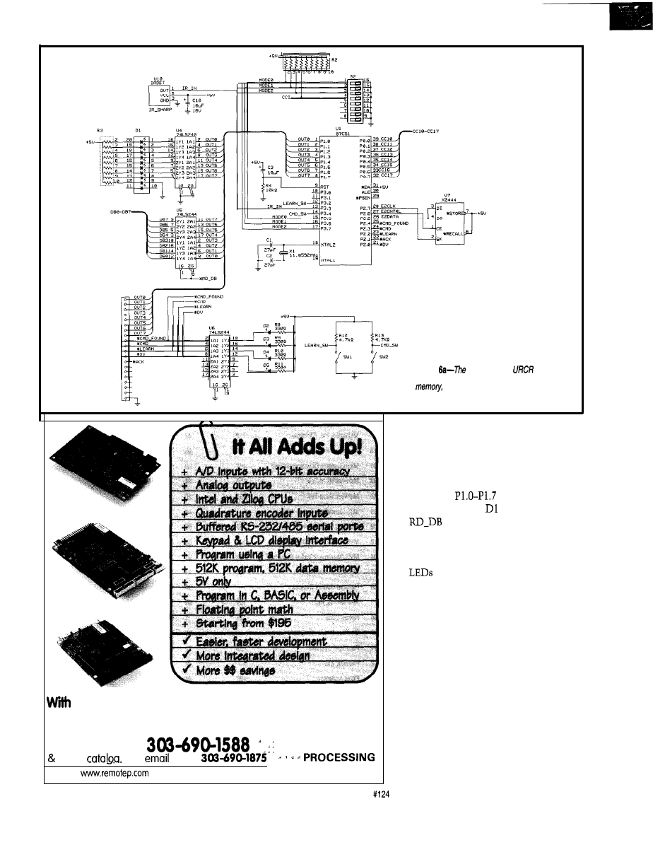
Figure
first ha/f of the
schematic
shows connections for the microprocessor,
mode selection, Learn and Cmd
buttons, and displays.
our line of embedded controllers and accessories,
everything adds up to make your job a success!
For more information
REMOTE'"
FREE
call.
or fax:
Web Site:
infoQremotep.com
The embedded control company
The customer code is input on Port
0 and can be set by the PC or switch
S 1. If you want to set customer codes
by the switches, S2.4 is turned on.
The decoded IR commands are
output on
and can be viewed
on the LED pack or read by the PC.
must be taken low to read the
data. These signals are inverted in the
PC. SW1 and SW2 are used to program-
ming the URCR in Modes 3, 4, and 5.
D2, D3, and D4 display current
status of the programming cycle.
The URCR eval board interfaces to
the PC via the parallel port. You need
a bidirectional parallel port, but most
new PCs are bidirectional capable.
ECP (Extended Capabilities Port) and
EPP (Enhanced Parallel Port) ports are
also compatible.
The parallel port interface can set
the customer code and read the data
bus (decoded IR commands and cus-
tomer codes). It also monitors the
programming cycle and DV, and it
controls ACK.
Sample PC parallel port interface
code is available for the evaluation
66
Issue a2 May 1997
Circuit Cellar INK@
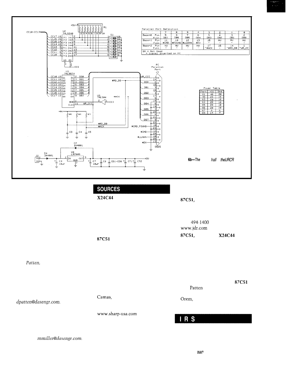
Figure
second
of
schematic shows connections for the parallel
port
interface,
power
supply, and customer code
selection.
board. A fully functional menu-driven
program is supplied with the URCR
eval board, and the PC code is DOS
compatible.
FINAL THOUGHTS
We hope this article solves some of
the mysteries of IR remote control.
With the basics of an IR remote-con-
trol standard, a few parts, and some
code, you can realize a system that
easily decodes many different types of
remote controls.
q
Daniel
an electrical engineer
at DAS, designs data-acquisition sys-
tems and custom computer hardware.
As well, he designs high-performance
audio equipment and speakers, re-
cently completing a.25W single-ended
class A amplifier. You may reach him
at
Michael Miller is an electrical engineer
at DAS. While he primarily develops
firmware and software for custom
hardware, he also collaborates on
custom hardware design. You may
reach him at
Xicor
15 11 Buckeye Dr.
Milpitas, CA 95035
(408) 432-8888
Fax: (408) 432-0640
www.xicor.com
Philips Semiconductors
811 E. Arques Ave.
Sunnyvale, CA 94088-3409
(801) 264-8050
Fax: (708) 296-8556
www.semiconductors.philips.com
IR Module
Sharp
5700 NW Pacific Rim Blvd., Ste. 20
WA 98607
(360) 834-8700
Fax: (360) 834-8611
NEC Electronics, Inc.
2880 Scott Blvd.
Santa Clara, CA 95050-8062
(408) 588-6000
Fax: (408) 588-6130
www.nec.com
Switches, LED, Crystal
JDR Microdevices
1850 S. 10th St.
San Jose, CA 95112-4108
(408)
IR Module,
Marshall Industries
9320 Telstar Ave.
El Monte, CA 9173 l-2895
(818) 307-6000
Fax: (818) 307-6187
www.marshall.com
URCR Components, URCR Evalua-
tion Board, Programmed
Dan
1768 N. 980 W
UT 84057
(801) 434-7226
416 Very Useful
417 Moderately Useful
418 Not Useful
Circuit Cellar
Issue 82 May 1997
6 7
DEPARTMEN
From the Bench
Silicon Update
TS
Joe
Standards for Electromagnetic
Compliance Testing
Testing Houses
basic
‘standing of EM1
standards and tests is
,
important to all designers
of electronic equipment. After all, it
doesn’t matter how well your equip-
ment performs its task. If it fails EM1
testing, you can’t ship.
Most electronics designers know
that EM1 tests are de facto design speci-
fications and that knowledge of these
tests is essential. Parts l-3 present the
most common emission and immunity
standards and tests required by the
FCC and European Community.
Understanding EM1 tests and stan-
dards is not only necessary for the
design of electronic equipment, but it’s
also important when it comes to taking
your equipment to be tested. So, this
article deals with the process of taking
electronic equipment to EM1 test labs.
Many designers spend hours review-
ing the EM1 tests and designing their
products to meet them. However, they
spend little time selecting a lab or
preparing for the tests. But, the selec-
tion of the test lab and what’s done
before, during, and after greatly affect
your product’s chances of passing.
When I look back on my first lab
test, I realize
I
did many things wrong
and was only lucky to get away with it.
The first mistake was in how I selected
the test lab.
68
Issue 92 May 1997
Circuit Cellar INK@
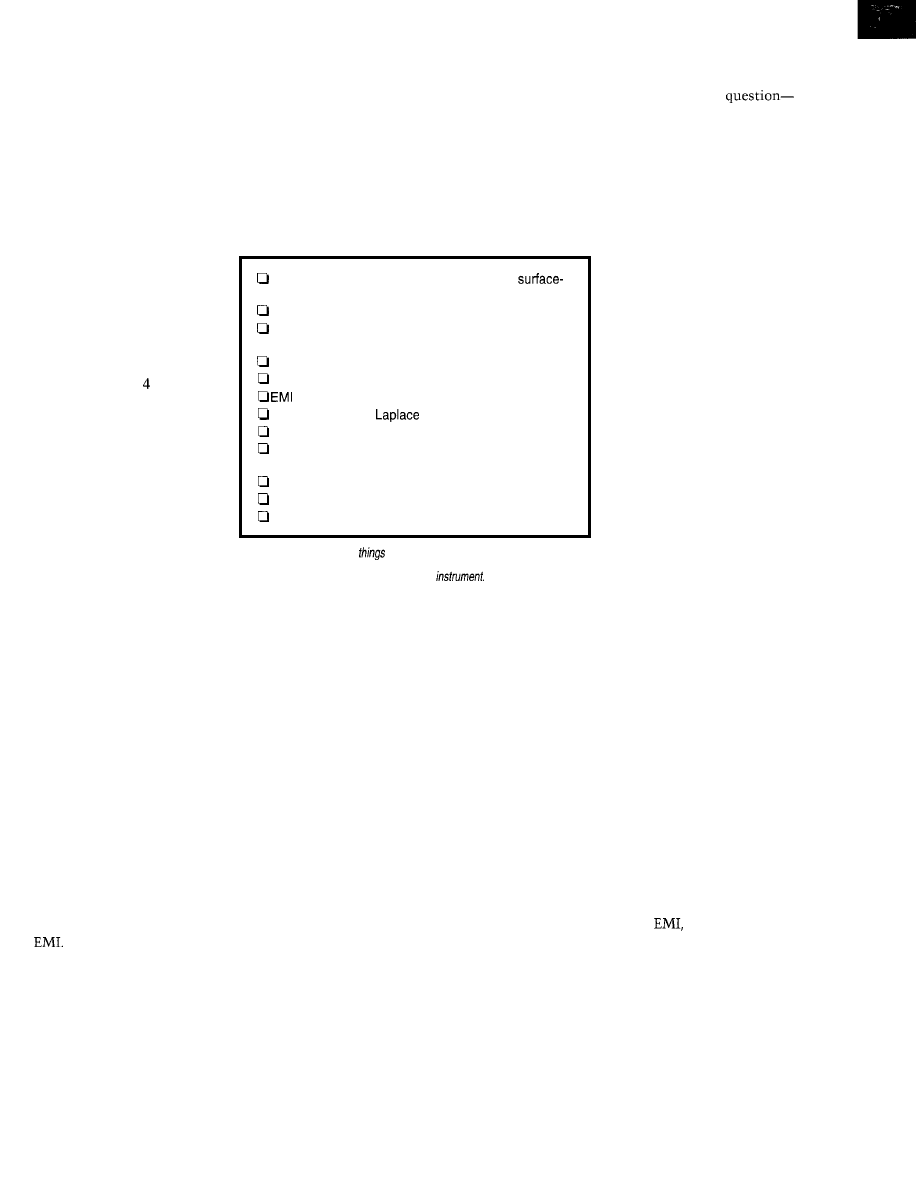
Since I live in metro Toronto, I have
some choice about which lab to use.
To select a test lab, I started by listing
important characteristics-experience,
quality of test equipment, flexibility of
scheduling, price, recommendations of
others, personnel, and so on. I then
categorized the factors by their pri-
mary and secondary importance.
because they’re on a tight schedule.
They may not be able to test your
product for another three months.
time that you are at the lab working
on your product?
Next, I determined the most impor-
tant characteristic in each
group. This gave me what I
considered the number-one,
most important factor in se-
lecting an EM1 testing labora-
tory-geographical proximity
to our manufacturing facility.
The key point is that your product’s
stage in its life cycle has a great bear-
ing on the lab you use. In the early
stages of a product’s life span, there are
more likely to be design changes. Then,
you want a flexible lab that tests you
when you’re ready.
Of course, this begs the
why not always go to a lab with a
flexible schedule? Well, to accommo-
date you, the lab had to delay someone
else. So, don’t be surprised if on occa-
sion that same lab delays you.
Whether or not you can live with
the odd delay is up to you. I work for a
small R&D company, and
having a flexible lab is impor-
tant to me.
Soldering iron, especially if your product has
mount components
Magnifying Glass
Various values and sizes of capacitors, resistors, and
inductors
At the time, it seemed
reasonable. With million
people in Toronto, traffic is
always bad. And of course,
there’s always the weather.
Toronto has some of the best
weather in Canada, but that’s
not saying much.
Ferrites, both individual and clamp-on-cable type
Voltmeter
probes
Filter topology and
transform table
Conductive tape and aluminum foil
All peripheral cables needed to run your instrument in
normal and worst-case modes
List of possible failure and remedial strategies
Notebook (Remember to take good notes!)
Test plan
All and all, I thought that
choosing a lab based on how
close it was to the office was a
good idea. I got away with this
error solely because that lab
happens to be excellent and fit
my needs perfectly.
On my first trip to the lab, I met a
Figure l--Here are some
you
should be sure to take along to the test
lab. Many of these items may seem obvious, but they’re often forgotten. Supple-
ment this list as necessary for your particular
fellow from Pennsylvania. Of course, I
asked him why he drove all the way to
Canada to perform FCC tests. He said
it was because of the quality of the lab.
I thought he was nuts.
Later, when the product has passed
EM1 testing and you’re testing for QC
purposes only, you need a lab that has
fixed schedules. At that point, any
delay in your QC testing delays ship-
ping the whole run.
lab, select the standards and tests you’ll
seek compliance under. This task
should be done in conjunction with
the test lab.
Prior to meeting with the lab, make
a list of the tests you think your equip-
ment needs to pass. In making the list,
anticipate most of the questions the
test lab will ask you. This approach
enables you to communicate intelli-
gently with the people at the test lab
and to determine which tests are ap-
propriate for your equipment.
EXPERTISE
The expertise of the lab is
also very important. Good,
experienced test technicians
are worth their weight in gold.
They’ve seen a lot of problems
and can usually offer good
suggestions.
Some labs have several EM1
engineers on staff to help you
with every aspect of the EM1
process from design to testing.
All these experienced people
are usually more expensive.
You must decide whether you
need that expertise or not.
Once you’ve chosen a test
But, now I understand that finding a
lab that fits your needs is crucial and
can have a huge impact on the length
of time it takes you to get your equip-
ment passed. Here are some thoughts
on selecting a testing lab.
RECOMMENDATION OF COLLEAGUES
Let’s
say that you’re in the middle
of designing a new product and you
plan to get the prototype tested for
Ask your colleagues to recom-
mend a lab.
When you call the lab, they’ll give
you a test date in about three months.
Two months later, you may realize
your prototype won’t be ready on time
and that you need an extra two weeks.
At that point, you may call the test
lab and find that they can’t fit you in
FLEXIBILITY
The flexibility of lab schedules is
more important to equipment early in
the product’s life cycle. But, it could be
important at later stages as well.
Let’s say you have a mature product
you gave a minor retrofit to. When you
take it to the lab, you find that the
minor retrofit causes major EM1 prob-
lems. You then realize that you need
an extra day to complete the tests.
Will the lab accommodate you by
delaying someone else’s tests? Can you
work on the instrument at the lab?
Almost every lab understands that
you may have to add a capacitor here
and there, but what if you have major
modifications that take several hours?
Can you do them and then continue
testing? Will you be charged for the
Keep in mind that the test lab has
no idea what your product does. They
see hundreds of products a year. If you
can explain your product’s function
with respect to
you’re more likely
to get the proper test set the first time.
It’s fairly common for test labs to
add tests once they get a feel for the
equipment. Also, prior listing of the
tests enables you to gauge your under-
standing of the EM1 issues and feel
comfortable about the final test list.
Good communication avoids a
situation like I experienced when a
Circuit Cellar INK@
Issue 82 May 1997
69
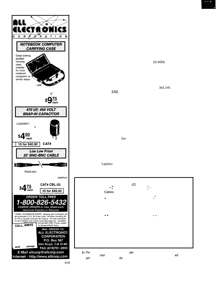
ment. Black
leatherette exterior
separate zippered compartment for papers or
accessories. Detachable nylon web shoulder
strap. Interior space is 13.5” X X 2.5”
CAT # CSE-12
Nichicon
MHSC
1.375” diameter 2” high.
0.4” lead spacing.
EC-4745
25 foot
50 ohm co-ax cable with
male BNC connectors molded with strain relief
on both ends. Ideal for studio, lab or
cations use. Inquire for quantity pricing.
FAX or E-MAIL
for our FREE
96 Page
CATALOG
Outside the
U.S.A.
_ _ _ _
$2.00
test
lab wanted to prescribe AC testing
for my battery-powered instrument. I
immediately labeled them a bunch of
crooks and dismissed them from my
lab search. In looking back, however, I
had to question whether or not I told
them that my instrument was always
battery powered.
The next big mistake I got away
with was not being prepared. During
the testing of my equipment, it was
discovered that 8
1
MHz was being
radiated. I had no idea from where, and
what was worse, I had very little in my
tool box to solve the problem. Because
I was close enough to my office, I was
able to get the components I needed.
drawing of filter topologies is often
very useful, as is a
transform
table.
Being prepared and anticipating the
problems is crucial. With
you
make your own luck. The better pre-
pared you are, the “luckier” you’ll be.
In preparing to go to the test lab,
there are several things to do, regard-
less of what stage your product is at.
First, pack a full tool kit that in-
cludes the items listed in Figure 1. The
lab may have a good selection of tools,
but don’t count on it.
A good solder iron is critical. Bring
a full set of capacitors, resistors,
rites, and inductors. I use the designer’s
kits
I
get from the manufacturers.
With the ferrites, bring both the
beads and the cable-clamp type. A
Another nice thing to have in the
toolbox is conductive tape or alumi-
num foil for shielding or plugging up
RF “holes.” Spare boards are also a
good idea, especially if you’re doing
immunity testing.
For each board and/or subassembly,
a list of all frequencies that can be
emitted helps you identify where the
radiated emission is coming from.
For example, if your microprocessor
board has a
clock, it’s reason-
able to expect that you may see the
fundamental and odd harmonics of this
frequency.
Of course, you must keep in mind
that the frequencies emitted will not
be the exact
lst,
etc. harmon-
ics because digital signals are trapezoi-
dal, not squares. But, the frequency
values should be close. A list of all the
technologies and their rise times gives
you an idea of possible frequencies
that can be emitted.
Bring both internal and external
cables of different lengths. Although
any wire radiates or receives any fre-
quency, cable length has a great deal to
do with the amount of radiation emit-
ted or received.
double-shield cables.
If you’re doing immunity testing,
you’ll most likely do Electrostatic
Also, bring some means of making
cables. And, if your cables are not
shielded or twisted, you should bring
some. If your cables are shielded, bring
Instrument or
cables?
I/O
Instrument
.
Remove one cable at a
Find RF hole, look for holes where the
time till the affected cable
longest dimension of the interfering
is found
frequency is a minimum of h/20
Once affected cable is found,
Once the RF hole is found, if due to
l
Shield cable
l
Seams, use
RF gaskets
l
Change cable length
l
Ventilation slots, use
mesh to reduce
l
Change cable type
the RF size of the hole
l
Change cable connectors
l
Connector port, use properly
l
Put
ferrites on cable
grounded metal connector
Figure
simplified flowchart shows a possible
of action if equipment fails radiated immunity tests. Of
course, you’ll expand this
to reflect your particular instrument. Keep in mind that any solution
be a
permanent
of your instrument, so keep cost of the solution in mind!
7 0
Issue 82 May 1997
Circuit Cellar INK@
Discharge (ESD) and Electrical Fast
Transients/Bursts (EFT/B) tests. So,
you’ll want surge suppression, MOV,
and the like.
Also, prepare boards that have surge
suppression on all the I/O and power
lines. If you have a transient problem,
these help identify the location quickly.
Research. What you find may sur-
prise you. Here’s a couple of examples.
In school, we all learned that a
signal traveling in coax cable is com-
pletely shielded. The signal travels
down the center conductor, and the
outer shield prevents any signals from
entering or escaping from the cable.
Unfortunately, the shield is never
perfect. If it’s a solid conductor, it
breaks. If it’s a braid, it’s leaky.
As the frequencies increase, the
inductance of wiring increases. At
a wire has more inductance
than resistance. So, the concept of a
good RF ground comes into play. Many
engineers use an ohmmeter to check
the impedance of ground connection.
Unfortunately, they’re only testing the
ground at DC.
Next, make a flowchart of possible
failures and the actions you can take.
Let’s look at a couple of tests. Imagine
a failure. What would you do?
TESTING EXAMPLES
Imagine that your
based system radiates 152 MHz at a
level that’s unacceptable. First, as you
see in Figure 2, you must determine
whether it’s from your I/O cables or
from the unit. Disconnect the I/O
cables, and test again.
If the problem is a cable radiating,
try different lengths of cable, shield
the cable with conductive tape or alu-
minum foil, use ferrite clamps, or place
passive filters on the line. Only you can
determine the best order to try these
solutions since you know your equip-
ment.
If the unit is causing the radiation,
first decide whether it’s the processor
clock or some other signal. Try reduc-
ing the clock rate of your processor.
Some microprocessors have this
facility built in. The Motorola 68333,
my personal favorite, makes it easy to
change the clock rate. With
flash, it can be updated via RS-232.
Channel Digital Oscilloscope
100
max single shot rate
samples
per channel
Advanced Triggering
Only 9
and 6.3” x 3.75” x 1.25
Small, Lightweight, and Portable
Parallel Port
interface to Laptop
‘Advanced Math, TV Line Trigger,
and FFT Spectrum Analyzer options
$499 you get the model
DSO-2102
Oscilloscope,
Probes, Interface Cable,
Adapter, and Windows and DOS Software.
l
200
max single shot rate
l
2 oscilloscope channels
l
8 Logic Analyzer channels
l
10 channels simultaneously
l
125 MHz Single Shot Bandwidth
l
up to
Samples/Channel
l
FFT and Spectrum Analyzer
(1
64k) $1999
DSO-28464
64k) $3299
All prices include Probes and Software
l
40 to 160 channels
l
up to 500 MHz
l
Variable Threshold
l
8 External Clocks
l
16 Level Triggering
l
up to 512K
40CH)
$1350
80CH)
$2000
40CH)
$1900
80CH)
$2800
LA451
28K
$7000
All prices include Pods and Software
Call for information on our
100
Pattern Generator option
L i n k I n s t r u m e n t s
369 Passaic Ave
l
Suite 100
l
Fairfield, NJ 07004
l
Fax (201) 808-8786
Web:
Circuit Cellar INK@
Issue 92
May
1997
71
PC
No M
ORE
C
RASH
B
URN
EPROM
Technology
DOS Single
Computer
572 k FLASH Memory
disk drive
Mhz CPU 2 Timers
512 k bytes RAM
4 Interrupt
512 k/256 k FLASH 8 Analog Inputs
2 Serial Ports
X-Modem File
24 Parallel I/O Lines
Transfer
INCLUDES DOS Utilities
8 Channels, 12 Bits
us. Conversion Time
Clock/Calendar Option
Includes Drivers &
8 Opto-Isolated Inputs
JK micros stems
Cost Effective Control
for
TO ORDER
our WEB site-www.dsp.com/jkmicro
1275 Yuba Ave., San Pablo, 94806
Other processors may require the crys-
tal to be changed.
If your problem is gone after you
reduce the clock rate, you probably
have an antenna (cable or trace) tuned
to
152
MHz on a line affected by the
processor frequency. If the radiation is
not affected by the microprocessor
frequency change, then look to other
clocks or oscillator sources.
Consider another possible scenario.
Your equipment hangs up during tran-
sient testing.
First, install the boards you made
with surge suppression on every line. If
that solves the problem, then isolate
the board by returning the original
boards one by one to the unit. Once
the board is located, find the individual
line and put surge suppression on it.
Some designers may decide that
surge protection on every line is a good
design practice, but it depends on the
equipment. If it’s a high-end product, a
few extra dollars don’t matter. For
cost-sensitive equipment, a few extra
dollars are the profit margin.
Remember how you pass the tests
determines how you build the equip-
ment. If you pass the test with every
line surge protected, that’s how the
equipment must be built and sold.
PRECAUTIONS
This may seem like overkill, but
keep a few things in mind. The labs
are very busy, so use time wisely. If
you have one day booked, don’t spend
half a day making cables.
When you arrive at the lab, make a
test plan for each test to be efficient.
You don’t want to wait while the test
technician decides what test to do next
and then finds they’re missing the
proper antenna.
Time is money. Know the order of
the test, and make sure that the lab
and you have everything necessary. If
you need something, get it while an-
other test is being run.
During the test, don’t just sit and
watch. Take careful notes of the test
setup and equipment. Ask questions. It
may slow down the works, but your
notes may be of great value.
If you’re failing, experiment at the
lab as much as possible. They have the
test equipment. Here, your flowchart
is crucial. Under pressure, you don’t
have time to think about what to try
next.
Document well what you tried that
didn’t work. Not only is this informa-
tion very valuable, but you’d be sur-
prised how many times the same
thing is tried.
COMING HOME
When you get back to your office,
whether you pass or fail, document
what happened. If you passed, the
information will be useful for your
next trip. If you failed, the notes will
help you discover a solution to the
problem.
Look at EM1 tests as sudden-death
exams. You could be passing every
test, but if you fail one, you can’t ship.
Of course, there are plenty of other
things to learn about EM1 standards
and testing. However, a basic under-
standing is the first priority since the
standards and tests are design specifi-
cations. And, by far, the best place to
handle EM1 is at the design stage.
q
P. Eng., has over
15
years’ engineering experience. He
currently works for Sensors and Soft-
ware and also runs his own consulting
company, Northern Engineering Asso-
ciates. You
reach foe at
sympatico.ca or by telephone at
FCC, Code of Federal Regulations,
Title 47, Parts 15 and 18, 1995.
IEC Standard 1000-4-1, Electromag-
netic Compatibility, Testing and
Measurement Techniques, Over-
view of Immunity Tests, Basic
EMC Publication, 1992.
C. Marshman, The Guide to the
EMC Directive
EPA
Press, Ambo, UK, 1992.
T. Williams, EMC for Product De-
signers, Butterworth and
mann, Oxford, UK, 1996.
419
Very Useful
420 Moderately Useful
421 Not Useful
72
Issue
82
May
1997
Circuit Cellar INK@
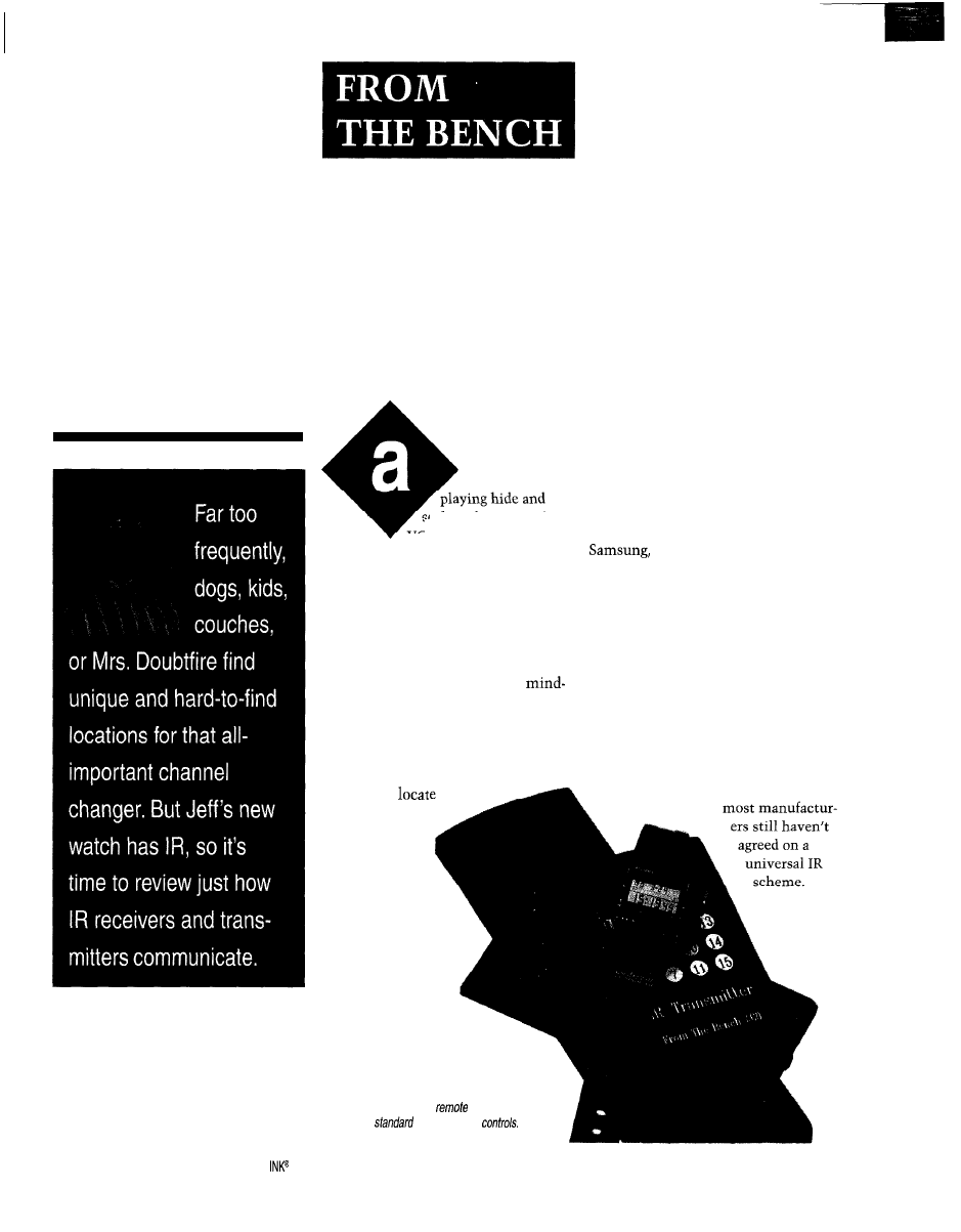
Infrared
Remotes
Jeff Bachiochi
are Everywhere...
If You Can Find ‘Em
re you constantly
seek with your TV/
VCR/audio/CD/cable/
satellite/toaster-oven remotes? At our
house, trying to find the remote is like
hunting down the mates to those odd
socks in the dresser drawer.
We own a piece of furniture espe-
cially designed for remotes (along with
the latest TV and cable guides). But
when I sit down to view a bit of
numbing entertainment, there’s no
listing guide in sight, never mind a
remote. It’s quicker to find the daily
listing in the newspaper and walk over
to the TV to change channels
than it is to
the surfing tool.
Not long
ago, I saw a
commercial for
a device that
attaches perma-
nently to the
back of the
clicker and pro-
duces a beeping sound to help you
locate it. But what happens when you
lose the remote’s remote?
I enjoy a good gadget as much as
anyone, but initially, I had my doubts
about a recent gift I got. A watch is a
noble gift to give or receive. One of my
favorites has a calculator built in, but
the keypad didn’t last.
This time around, I wasn’t going to
calculate. This watch has an IR trans-
mitter built in. At first, I thought,
“Gimmick,” but then, I found it re-
placed the remotes I could never find.
This month’s project takes advan-
tage of this transmitting timepiece.
CASIO WRIST REMOTE
This watch, shown in Photo 1, is
like having an all-for-one IR remote
with you at all times. It’s compatible
with most TV, cable, and VCR equip-
ment made by today’s leading manu-
facturers-GE, Goldstar, Hitachi,
Jerrold, JVC, Magnavox, Mitsubishi,
Panasonic, Philips, Pioneer, RCA,
Scientific-Atlanta, Sharp,
Sony, and Toshiba.
Although there’s no full-function
keypad, you can still access most im-
portant functions-power on/off, chan-
nel up/down, volume up/down, play,
fast forward, rewind, and stop.
Unlike many Windows applications
with their pop-up help menus, this
Casio requires a small instruction
booklet. Once the manufacturer codes
are set, the reference is not necessary
until you get a new piece of equipment.
The first thing you notice is that
Photo l--The Casio wrist
replaces
many of the
AN IF? remote
74
Issue
82 May 1997
Circuit
Cellar
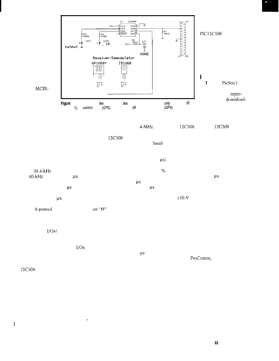
That’s why you have
to set specific codes.
To be able to recog-
nize IR codes, you
must know a little
about them. If you
don’t have a scope
handy for experiment-
ing, you can gain a
bunch of insight from
Ed Nisley’s article on
the MCIR-Link (“Ex-
tending Your Control:
The HCS II
Link,” INK 29). Al-
though I have a scope,
Relay
&Received
IR
““G
“G”
To PC
it isn’t a storage scope,
l--The circuit shows test setup for project. The finished circuit
requires an
so
it doesn’t lend itself
input (GP the
output
and an optional received LED output
to
capturing pulse trains.
I decided to create a tool to analyze
various signals’ bursts. It served as the
front end of the project and reduced
the programming.
The first objective was to look at
various signals and find simple ways of
identifying them. I wanted a real-time
display of just what was happening.
Most IR transmissions are actually
bursts of a
carrier. A single
cycle of
carrier lasts 25
The
demodulator needs a minimum burst
of a few cycles. I picked 250 as a
sample time. Most minimum bursts
seem to be around 500
One of Microchip’s newest little
chips is an
processor-cer-
tainly far from what most would con-
sider the minimum computer. After
all, what can you do with a computer
that has only 4-6
Actually, quite a lot! With an inter-
nal RC oscillator, all the pins except
power and ground can be used as
(The internal RC oscillator is factory
trimmed to 4 MHz.)
This month’s project is designed for
the
Keep in mind that the full
project requires two programmed de-
vices-the first to gain information and
the second to use that stored info in a
permanent fashion. The device is an
OTP, but windowed parts are available.
To give real-time data analysis, I
chose to send characters out a port pin
serially. At 9600 bps, that works out to
about 2.5 bits of a character. Hmmm..
could quickly see that I needed to do
at least 57.6 kbps, if not 115 kbps, just
to
send a single character and have
some time left to do something else.
Because I like using a
crys-
tal, which gives l-us instruction times,
and the
was fixed at 4 MHz, I
knew I was going to have some
rate timing errors. Calculations showed
roughly 2% for 57.6 kbps and 4% for
115 kbps (rounding to the nearest 1
I went with the 2% error. RS-232
communications can easily handle 2
This choice enables me to send a single
character
(10
bits at 17 per bit) for
each sample and still have 80 left.
Since what I was wanted to see was
how the IR was going to be interpreted
by the micro, I went for simple. Send
if the sample was logic high and
“L” if the sample was logic low.
In addition to sampling the demod-
ulated IR and sending out a reflection
of the sample’s logic level, I tracked
the number of consecutive times the
same logic state was sampled. Using a
single-byte counter allowed for a steady
logic state of 64 ms (250 x 256). A
state that lasted that long was illegal.
An illegal state causes the serial
output bit to be redefined as an input
bit and therefore halts any further
output to whatever serial device I had
it connected to. The serial device may
be a printer or a smart/dumb terminal.
Either way, it prevents the data from
spooling endlessly once the IR is re-
moved (i.e., it stopped changing state).
I’m a crash’n’burn guy. The chances
of my program running the first time
out of the gate are nil, even with a bit
of time spent with the simulator.
My objective was to
create code that could
be used with the little
processor.
However, I’d probably
have to go through a
bunch of OTP devices
or else spend all my
time in front of the
EPROM eraser. So..
CHEATED
used a
Its
code space is EEPROM
and electrically
grammable. I
ed compatible assembly
code (hex file) to it and
used it for development.
Once the code ran, I reassembled for
the
Since the
doesn’t
have a UART or interrupts, the serial
needed to be bit banged.
In addition, the rest of the code had
to be cycle counted such that each
possible code path always took exactly
the same number of instruction cycles.
If the serial and sample loop was cor-
rectly timed, samples could be accu-
rately taken each 250
I also cheated on the RS-232 connec-
tion. To eliminate the MAX232 (used
in good designs) for conversion of TTL
to
RS-232 signals, I produced an
inverted TTL serial output. Although
not good design practice, I’d only use it
for analysis and it wouldn’t be neces-
sary for the final product’s operation.
Note in Figure 1 how the serial
output line is pulled to ground. This
feature keeps glitches from looking like
start bits to the serial device whenever
the output pin is reconfigured as an
input pin.
Using
I captured my
first visual glimpses of the (demodu-
lated) IR produced by the Casio. As I
input various manufacturers’ codes
and saw evidence of different kinds of
coding, I thought I may have bitten off
more than I could chew.
I
soon realized, however, that I
ultimately wanted to simply turn on
or off one of the micro’s outputs by
recognizing an IR code. Therefore, I
didn’t necessarily have to completely
understand every transmission scheme
used by all the manufacturers.
Circuit Cellar INK@
Issue May 1997
7 5
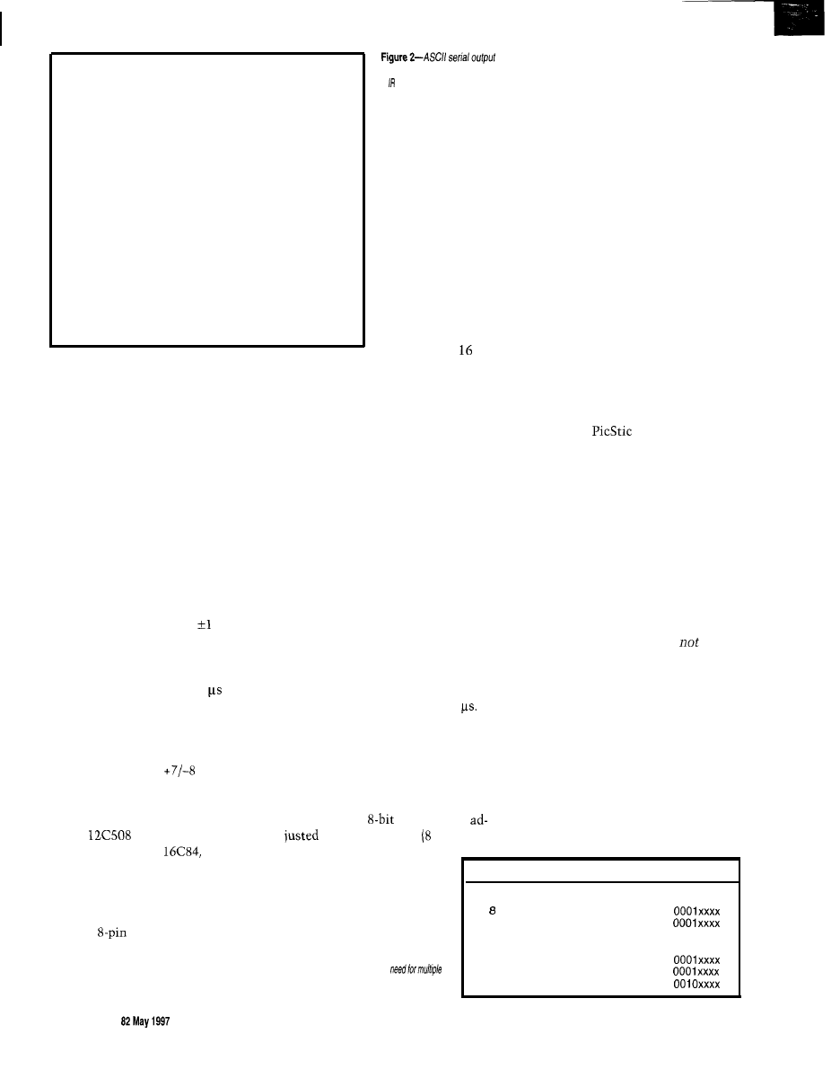
LHHHHHHHHHHHHHHHHHHHHHHHHHHWHHHHHHHHHHHHHHHHHHHLHHHHHHHHHHHHHHHHHH
HHHHHHHHHHHHHHHHHHHHHHHHHHHLLHHHHHHHHHHHHHHHHHHHHHHHHHHHHHLHHHHHH
HHHHHHHHHLLHHHHHHHHHHHWHHHHHHHHHHHHHHHHHHHHHHHHHHHHHHHHHHHHHHHHHHH
HHHHHHHHHHHHHHHHHHHHHHWHHHHHHHHHHHHHHHHHHHHHHHHLLHHHHHHHHHHHHHHHHH
HHHHHHHHHHHHLLHHHHHHHHHHHHHHHHHHHHHHHHHHHHHLLHHHHHHHHHHHHHHHHHHHH
HHHHHHHHHHHHHHHHHHHHHHHHHLHHHHHHHHHHHHHHHHHHHHHHHHHHHHHHLHHHHHHHH
HHHHHHHHHHHHHHHHHHHHHHHHHHHHHHHHHHHHHHHHHHHHHHHHHHHHHHHHHHHHHHHHH
HHHHHHHHHHHHLLHHHHHHHHHHHHHHHHHHHHHHHHHHHHHHHHHHHHHHHHHHHHLHHHHHH
HHHHHHHHHLHHHHHHHHHHHHHHHHHHHHHHHHHHHHHHLHHHHHHHHHHHHHHHHHHHHHHHH
HHHHHHHHHHHHHHHHHHHHHLLHHHHHHHHHHHHHHHHHHHHHHHHHHHHHHHHHHHHHHHHHH
HHHHHHHHHHHHHHHHHHHHHHHHHHHHHHHHHHHHHHHHHHHHHHHHHHHHHHHHHHLHHHHHH
HHHHHHHHHHHHHHHHHHHHHHHLLHHHHHHHHHHHHHHHHHHHHHHHHHHHHHLLHHHHHHHHH
HHHHHLLHHHHHHHHHHHHHHHHHHHHHHHHHHHHHLHHHHHHHHHHHHHHHHHHHHHHHHHHHH
HHHHHHHHHHHHHHHHHHHHHHHHHHHHHHHHHHHHHHHHHHHHHHHHHHHHHHHHHHHHHHHHH
HHHHHHHHHHHHHHHHHHHHHHHLLHHHHHHHHHHHHHHHHHHHHHHHHHHHHHHHHHHHHHHHH
LHHHHHHHHHHHHHHHHHHHHHHHHHHHHHHHHHHHHHHHHHHHHHLHHHHHHHHHHHHHHHHHH
HHHHHHHHHHHHHHHHHHHHHHHHHHHLLHHHHHHHHHHHHHHHHHHHHHHHHHHHHHLHHHHHH
HHHHHHHHHLLHHHHHHHHHHHHHHHHHHHHHHHHHHHHHHHHHHHHHHHHHHHHHHHHHHHHHH
HHHHHHHHHHHHHHHHHHHHHHHHHHHHHHHHHHHHHHHHHHHHHHLLHHHHHHHHHHHHHHHHH
HHHHHHHHHHHHLLHHHHHHHHHHHHHHHHHHHHHHHHWHHHHLLHHHHHHHHHHHHHHHHHHHH
HHHHHHHHHHHHHHHHHHHHHHHHHLHHHHHHHHHHHHHHHHHHHHHHHHHHHHHHLHHHHHHHH
HHHHHHHHHHHHHHHHHHHHHHHHHHHHHHHHHHHHHHHHHHHHHHHHHHHHHHHHHHHHHHHHH
HHHHHHHHHHHHLLHHHHHHHHHHHHHHHHHHHHHHHHHHHHHHHHHHHHHHHHHHHHLHHHHHH
HHHHHHHHHLHHHHHHHHHHHHHHHHHHHHHHHHHHHHHHLHHHHHHHHHHHHHHHHHHHHHHHH
HHHHHHHHHHHHHHHHHHHHHLLHHHHHHHHHHHHHHHHHHHHHHHHHHHHHHHHHHHHHHHHHH
HHHHHHHHHHHHHHHHHHHHHHHHHHHHHHHHHHHHHHHHHHHHHHHHHHHHHHHHHHLHHHHHH
HHHHHHHHHHHHHHHHHHHHHHHLLHHHHHHHHHHHHHHHHHHHHHHHHHHHHHLLHHHHHHHHH
HHHHHLLHHHHHHHHHHHHHHHHHHHHHHHHHHHHHLHHHHHHHHHHHHHHHHHHHHHHHHHHHH
HHHHHHHHHHHHHHHHHHHHHHHHHHHHHHHHHHHHHHHHHHHHHHHHHHHHHHHHHHHHHHHHH
HHHHHHHHHHHHHHHHHHHHHHHLLHHHHHHHHHHHHHHHHHHHHHHHHHHHHHHHHHHHHHHHH
shows logic /eve/s received from
an transmission.
But, that’s getting
a little too far ahead.
First, I need to decide
how many durations
long the table will be.
I chose to use table
the chances of that
number reoccurring seemed highly
improbable.
For instance, one scheme (shown in
entries because
Figure 2) produced a pattern of 34 logic-
high duration cycles before repeating
the sequence. Comparing the patterns
produced by four different functions
[push buttons), I quickly saw that after
sampling the first three logic-high dura-
tions, I could easily tell which of the
buttons was pressed. Was that enough!
ENOUGH ALREADY!
Fact is, the same three-value combi-
nation can easily come up again in a
particular sequence. It also depends on
the tolerance of what’s considered a
match. Must values match exactly?
What about a deviation of count?
My experiments show that the
minimum duration of a logic high is
about 16 cycles (4 ms), while the logic-
low duration is always -500 for this
particular manufacturer’s code.
The logic-high durations also seem
to be in multiples of 16. It’s then easy
to see that a single compare with a
built-in tolerance of
can be
achieved by adding 8 to each sample
and making a compare, masking out
the low nibble shown in Table 1.
I stuffed them into RAM while in a
programming mode. Then, I switched
to a compare mode to quickly test new
sequences without physically program-
ming a table with them.
To make debugging easier, I pro-
grammed the sample counts to be
dumped at the end of either a program
or compare cycle. And, I added a
l-s
pause after each compare cycle. This
way, I could see what the micro was
seeing and a new compare wouldn’t
begin immediately.
STOP, LOOK, AND LISTEN
When the program executes, it looks
at the mode input pin to determine
which mode to run in. Programming
mode samples the IR every 250
Once a logic state remains constant
for 256 samples, it’s considered idle.
An idle state clears the table pointer
preparing to start a compare.
As an IR stream is received, each
high and low logic-level duration is
counted by an
counter. The
The
parts have no EEPROM
high-level counts
data storage like the
so the final
added and the lower nibble
table of numbers as sampled by the
masked off) are stored into
program needs to be placed in a table
sequential RAM registers.
along with the code that’s running.
You can also fit a number of tables
into this
package. Each table,
when matched to an incoming sample,
performs a different operation (e.g., set,
Table l--Eliminate the
clear, toggle, or pulse a particular bit).
compares by reducing resolution.
For some manufacturers, you may
need to save the low-level counts or
even both.
When the appropriate number of
duration counts are stored, an output
LED is enabled, indicating a successful
program cycle. In this mode, execution
stops until the programming mode bit
is grounded (compare mode).
Execution then continues in com-
pare mode. To resample (reprogram) an
IR sequence, leave it in programming
mode (input bit high) and reset the
processor.
Different programming practices are
used depending on whether the table
will be soft coded (programming mode)
into RAM or hard coded as a table. I
don’t envision this device being pro-
grammed by the user at the time of
installation. Instead, I think it should
come programmed for a particular code
(e.g., my Casio).
Using the
offers more op-
tions and flexibility, but this project is
intended to end up as an exercise in
minimum parts cost and size.
Independent of the storage type (i.e.,
RAM or code table), the compare pro-
cess is the same. At idle, the table
counter is cleared. In addition, a “good”
flag is cleared.
As the IR stream is detected, the
consecutive high-duration samples are
counted as before. Instead of storing an
adjusted count, it’s compared to the
corresponding table entry. If
equal,
the “good” flag is incremented.
The samples continue until the end
of the table is reached. The output
LED is enabled, signaling the end of a
compare. If the “good” flag is still at 0,
all entries matched and a good com-
pare function is performed. In this case,
an exclusive OR toggles the relay logic
output to the opposite state.
In both the program and compare
modes, once 16 samples are taken, the
sample counts are spit out of the serial
Decimal
Binary
Binary+8
High Nibble
7
00000111
00001111
ooooxxxx
00001001
00010001
9
00001010
00010010
22
00010110
00011110
23
00010111
00011111
24
00011000
00100000
76
Issue
Circuit Cellar INK@
output bit in ASCII. Now that I’ve
programmed the device from the se-
lected Casio function key and verified
that it compares correctly, I can use
these counts in the compare code table
used by the
microprocessor.
The final code placed in the
doesn’t require the programming mode.
Its compare table is hard coded and
cannot be changed. The serial output
bit isn’t needed anymore.
However, I don’t have to change the
code. I don’t need those functions. Just
three bits are necessary-the IR input,
the compare status LED output, and
the RELAY output. I’ll bet you can find
useful functions for those other bits.
This complete circuit can be built
into almost anything-a lamp, radio,
coffee maker, or door lock. The circuit
current is small enough to be powered
from an unisolated AC/DC circuit. No
bulky transformer is needed.
A 5-V relay can be directly driven
from the micro’s port pin for a
sensitivity model that doesn’t exceed
the micro’s source current. However, a
solid-state relay is a good alternative.
So, don’t be nervous about experi-
menting with new things. Use the
tools you already have to develop the
tools you need to explore new areas.
And, if you have any sure-fire ways
to keep the remote from getting lost,
please share them with me.
q
Bachiochi (pronounced
AH-key”) is an electrical engineer on
Circuit Cellar INK’s engineering
staff.
His background includes product
design and manufacturing. He may be
reached at
All the software tools I used to
develop this project’s code are avail-
able from Microchip’s Web site.
Digi-Key Corp.
701 Brooks Ave.
Thief Falls, MN 56701-0677
(218) 681-6674
Fax: (218)
Microchip Technology, Inc.
2355 W. Chandler Blvd.
Chandler, AZ 85224-6199
(602) 786-7200
Fax: (602) 786-7277
www.microchip.com
Micromint, Inc.
4 Park St.
Vernon, CT 06066
(860) 871-6170
Fax: (860) 872-2204
www.micromint.com
Sharp Electronics Corp.
Microelectronics Group
5700 NW Pacific Rim Blvd., Ste. 20
WA 98607
(206) 834-2500
Fax: (206)
422
Very Useful
423 Moderately Useful
424 Not Useful
The HAL-4 kit is a complete battery-operated
electroenceph-
alograph (EEG) which measures a mere 6” x 7”.
HAL is
sensitive enough
to even distinguish different conscious states-between concentrated
mental activity and pleasant daydreaming. HAL gathers all relevent alpha,
beta, and theta brainwave signals within the range of 4-20 Hz and presents
it in a serial digitized format that can be easily recorded or analyzed. HAL’s
operation is straightforward. It samples four channels of analog brainwave
data 64 times
per second and transmits this digitized data serially to a
PC
at
4800 bps. There, using a Fast Fourier Transform to determine
amplitude, and phase components, the results are graphically displayed in
real time for each side of the brain.
Contains HAL-4 PCB and all
components, source code on
PC
diskette,
serial connection cable, and four extra sets of disposable electrodes.
to order the HAL-4 Kit or to receive a catalog,
C A L L :
C
I R C U I T
C
E L L A R
K
ITS
l
4 P
A R K
S
T R E E T
S
UITE
12
l
V
ERNON
l
CT 06066
l
Circuit Cellar Hemispheric Activation Level detector presented as an
example of
the design techniques used in acquiring
signals. This Hemispheric Activation Level detector is
not a medically approved device, no
claims are made for this
and it should not be used for
medical
purposes.
safe use requires HAL be battery operated
Circuit Cellar INK@
Issue 82 May 1997
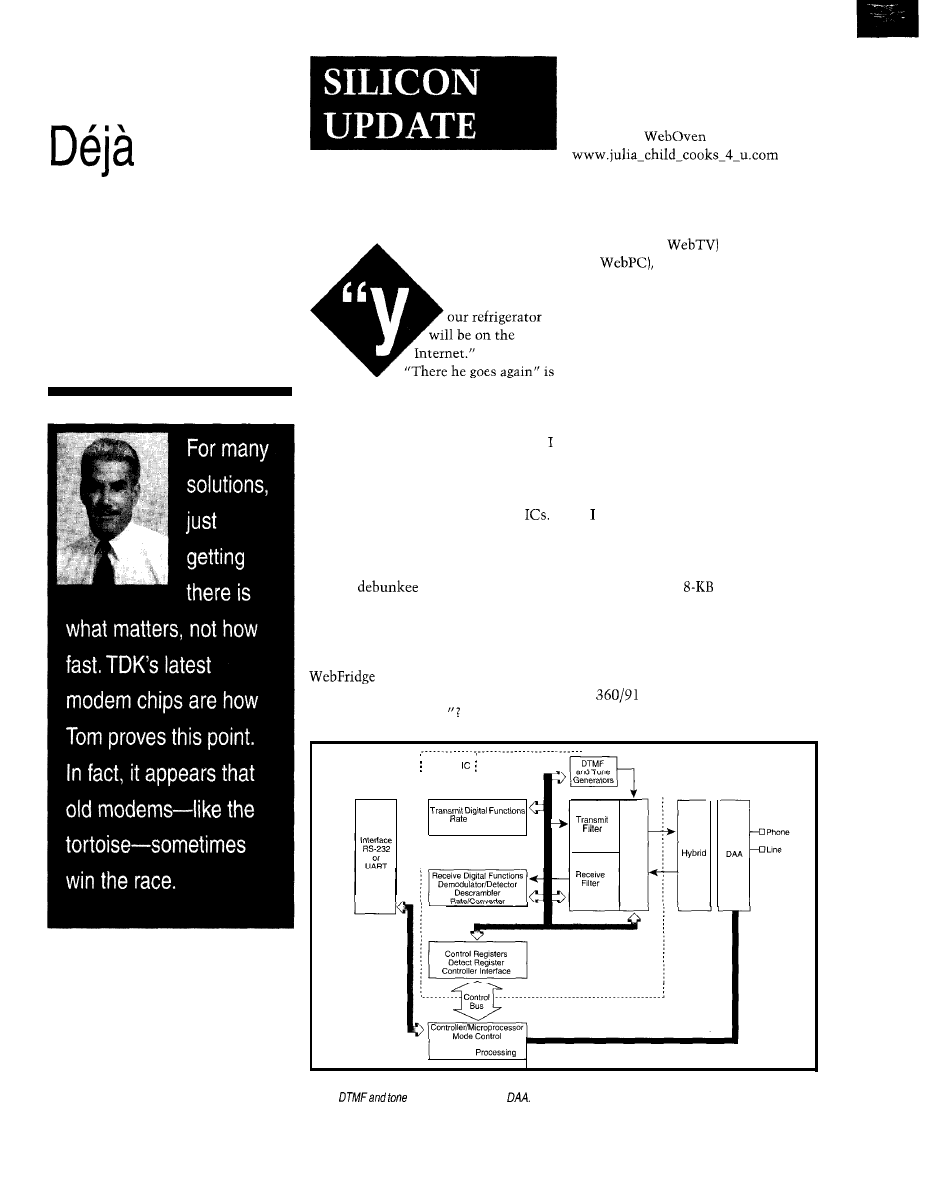
Modem
Vu
Tom Cantrell
probably what you (and my long-suffer-
ing editor) are thinking. It’s true I get a
little wild when it comes to prognosti-
cating about technology. It’s also true
usually end up being right.
Oh, by the way, the refrigerator
quote isn’t mine. Lou Gerstner, head
of IBM and hardly a wild and crazy
guy, said it. Of course, I happen to
agree that his vision will come true
someday. The question is: Will it be
sooner or later?
That’s because no special intellec-
tual or psychic abilities are needed to
predict a science-fiction future for
Just don’t specify a date.
DAYS OF MODEMS PAST
“In our lifetime” works especially
well since neither would-be debunkers
nor the
care much after that.
If you simply wait long enough, you
can rely on ever-improving chip price
and performance to prove you right.
can kind of remember my first
modem some twenty years back. At
that time, they (like all computer stuff)
were rather esoteric items. My budget
already blown on
RAM boards, I
tried to make do with a cheap [only a
couple hundred bucks!) build-it-your-
self modem kit.
Actually, it’s not hard to imagine a
It seemed to make the right sounds,
scenario. Who hasn’t cruised
and I did manage to get connected to
into the kitchen late at night only to
the
across town, but it was just
find “Arrgh! No milk!
too flaky to be usable. Nothing against
Already, grocery-shop-by-Web
services are sprouting up. Wouldn’t it
be great if your refrigerator could stock
itself? How about shoving a frozen
turkey in a
that dials up
and
takes it from there?
Admittedly, there are a few minor
obstacles to overcome. Embedding the
Web feature has got to cost tens, not
hundreds (e.g.,
or thousands
(e.g.,
of dollars. Also, the Web,
which appears to be running on the
ragged edge already, isn’t likely to
gracefully handle hundreds of millions
of appliances coming online.
Modem
converter
Scrambler Modulator
MUX
Handshake Control
Command
Figure l--This generic block diagram of a modem shows the major building blocks-modulator and demodulator,
filters,
generator, hybrid, and
78
Issue
92 May 1997
Circuit Cellar INK@
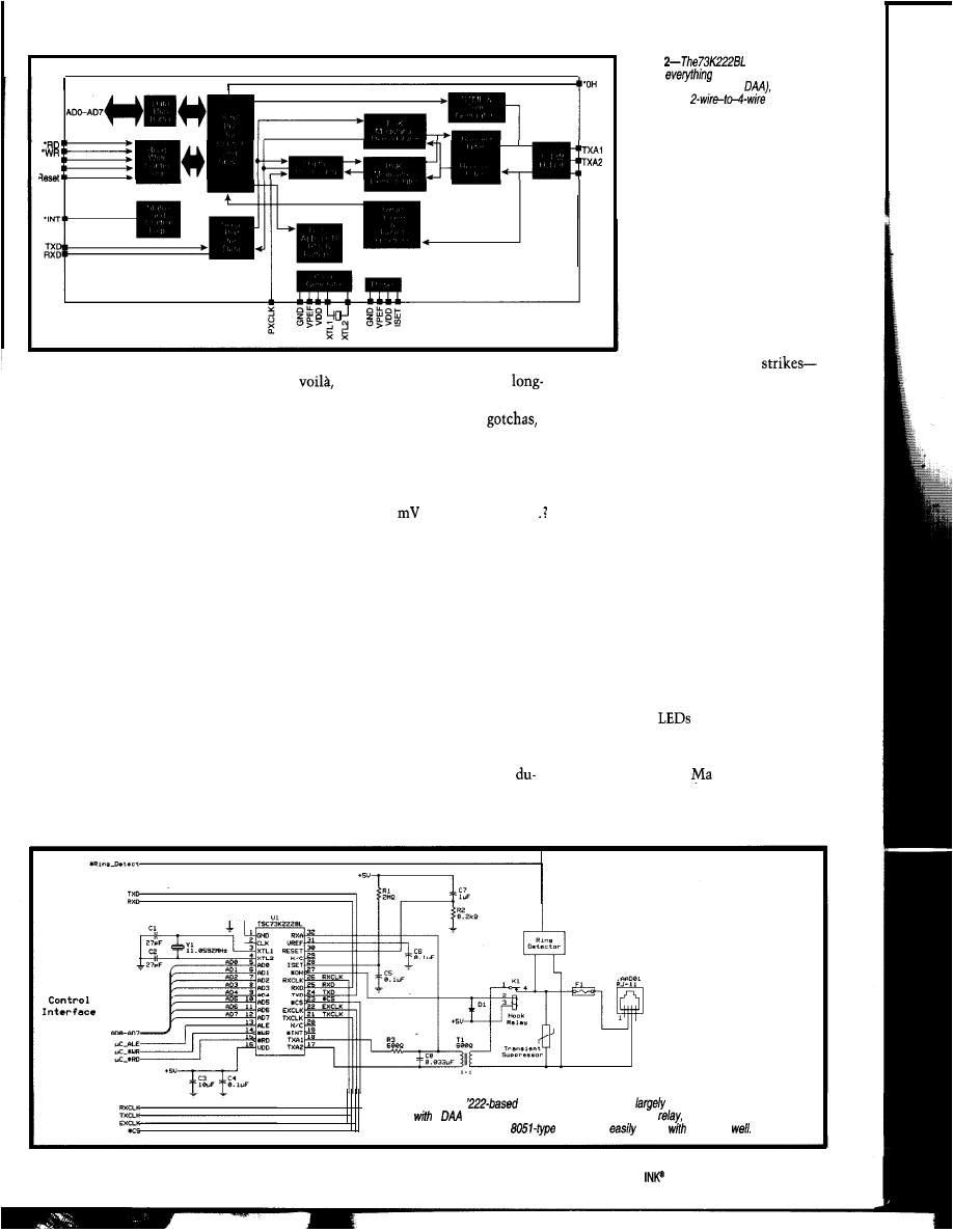
ALE
‘CS
RXA
the kit designer or supplier. It could be
that I just got one of the zillions of
resistors and caps wrong. In any case, I
had neither the tools nor the skill to
debug it and ended up just spending
more for a surplus commercial unit.
It’s not surprising I had problems
since modems are quite a black art.
The concept starts out simple enough
but runs into a witch’s brew of analog
foibles, regulatory restrictions, and
profligate standards as soon as you plug
into the phone jack.
Certainly at that time, the modula-
tor and demodulator (from which the
word “modem” is derived) were quite
straightforward. Simply allocate one
frequency for 0, another for 1, and have
at it-an approach known as FSK (Fre-
quency Shift Keying).
If you want simultaneous send and
receive (i.e., full-duplex), allocate four
frequencies-two for the originating
modem and two for the answering one.
Sample and update at 300 Hz, and
you’ve got the guts of that
ago (Bell 103 standard) 300-bps modem.
Of course, there are a few
the most critical being that the signal
can get ugly by the time it crosses hill
and dale. Your design may work great
with a clean 2-V signal in the lab, but
when it gets 20
in the real world..
Oh well, with all those op-amps you
need for filters, a few more for adaptive
gain won’t hurt. While you’re at it, be
sure to provide equalization since the
network is prone to attenuate and delay
some frequencies more than others.
Going beyond this so-called data
pump is where things get tricky. For
full-duplex operation, the outgoing and
incoming signals have to be joined. But,
you can’t just connect the wires since
simultaneous transmit and receive will
step on each other.
So, you’ve got to add a hybrid,
plexer, or 4-wire-to-2-wire converter
to put your transmission on the line,
but make sure you don’t hear it.
Figure
integrates
almost
between a micro and
the isolation barrier (i.e.,
up to and
including the
hybrid.
DAAT’S NOT ALL FOLKS
It gets worse. Though
lightning may not strike
twice, Murphy says it’s sure
to strike at least once just
about the time you jack in.
With consumer safety in
mind, UL zaps your box with
simulated lightning
the ultimate smoke test! It’s OK if
your gadget dies, but it must die qui-
etly without fireworks. Protection is a
two-way street, and the FCC (Part 68)
steps in to ensure the phone network
doesn’t suffer from your design goofs.
The result: all modems (indeed any-
thing connected to a phone jack) needs
an approved Direct Access Arrange-
ment (DAA) that bridges the isolation
barrier between your electronics and
the phone wire. Other functions that
cross the bridge include the off-hook
relay and ring detector.
You can use the relay for pulse dial-
ing, but these days, it’s best to throw in
a DTMF (Dual Tone Multifrequency)
touch-tone generator. Put it together
with flashing
and a speaker, and
you’ve got all the pieces of the modem
puzzle (see Figure 1).
In the old days,
Bell ruled the
phone wires, and Bell 103 was all there
was standards-wise, certainly in the
U.S. and maybe even worldwide. Since
Figure 3-A
modem design consists
of bridging the isolation barrier
a
comprising an isolation transformer, hook
and ring detector. The bus
is a direct connect to
micros but
mates
others as
Circuit Cellar
Issue 82 May 1997
7 9
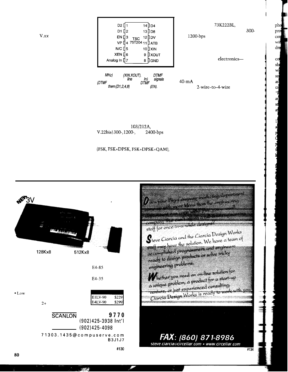
then, however, the high-tech equiva-
lent of the U.N. (CCITT) has blessed a
bewildering variety standards-all
those funny
numbers littering
modem ads.
Modulation has gotten more clever,
encoding more bits into each sample
by fiddling with phase (e.g., DPSK or
Dibit Phase Shift Key) and amplitude
(e.g., QAM or Quad Amplitude Modu-
lation) with the latest schemes cram-
ming up to 12 bits per sample. This,
combined with speedier sampling
(from 300 to 2400 Hz) is how we got
today’s fast modems (e.g., 2400 x
12 =
28.8
kbps).
Just to spice things up, remember
all these international standards mean
every country’s equivalent of UL and
FCC gets to bless your design, too. The
bottom line is modem design wasn’t
easy then, and it’s even harder now.
Fortunately, IC wizards ease the pain.
DIP WHISTLE
If you’re willing to sacrifice speed,
modem chips like the K-series from
TDK Semiconductor deserve a closer
Figure
4-Connected to an inexpensive TV color-burst
(3.58
crystal
the ‘204
receiver listens to the
(Analog and
Valid) the occurrence of
tones and
outputs
when enabled
look. While modem design is still
tough, the latest chips make it as easy
as it can, and pretty much ever will be.
The K-series comprises a family of
semiplug-compatible chips that cover
the popular (Bell
V.21, V.22,
and
standards. Essentially, the family line-
up is a matrix permuting modulation
host CPU interface (serial+parallel or
serial-only) and package (PLCC and
DIP). TDK also offers a couple of mod-
els with built-in PC-compatible UART.
Let’s take a look at a recent intro-
duction, the TSC
which
handles FSK and DPSK coding for
and
operation.
Figure 2 shows how the latest chips
make modem design as easy as can be.
The ‘222 incorporates practically all
the equipment-side
modulator, demodulator with all the
filters, call progress (e.g., dial tone,
busy, etc.) detection, DTMF generator,
off-hook relay driver, and now
even the
hybrid.
Notice that the chip goes as far as it
can toward the phone network. That
is, everything else (the DAA composed
of coupling transformer, off-hook relay,
and ring detector) has to cross the
isolation barrier as shown in Figure 3.
Thus, short of adding the processor,
it’s hard to imagine a more integrated
device on a single piece of silicon. You
still have to provide the DAA, by mak-
ing, testing, and getting your own de-
sign approved, or buying a preapproved
unit from a specialist like Cermetek.
The ‘222 includes serial and parallel
interfaces. The serial interface (TXD
EPROM EMULATORS
emulators from $229.00
El
up to
E4 up to
l
85ns and 35ns standard access times
Prices
l
3V LV
models operate at
3V and 5V
El-85
$199
l
High-speed downloading (LPTI -3)
$249
with error checking and correction
El-35
$229
l
Loads binary, Mot-S, Intel
$299
l
Power-up emulation
*Compact size, with protective case
power design, 5mA max.
l
Software configurable
*Discounts on
units
A-PLCC
$65
SDI
8 0 0 3 5 2
DESIGN
INC.
FAX
i n t e r n e t :
5 2 2 4 B l o w e r s S t . H a l i f a x , N S , C a n a d a
Issue a2
May 1997
Circuit Cellar INK@
and
and RXD) transfers data across the
To do so, however, the somewhat
phone line, while the parallel interface
sloppy timing (a couple of percentages)
provides access to on-chip status and
of the UART has to be cleaned up to
control registers and is compatible
meet the much stricter
syn-
with 805 1 and other multiplexed (ad-
chronous timing
Fortunately, the
dress/data) micros.
‘222 includes an ASYNC/SYNC.
Some models route both data and
control/status through the serial bus to
shrink into a 22-pin DIP. Even those
with the parallel bus offer a
serial interface scheme using ADO-AD2
as AO-A2 (to address the status and
control registers), AD7 as the data bit,
l
RD and *WR as direction, and EXCLK
as the clock. An ‘INT output requests
service on detecting dial tone, carrier,
and other line-status indicators.
Alternatively, you can switch to a
synchronous (computer-speak) data
format such as HDLC.
A number of suppliers (e.g., Zilog
and Motorola) offer
with inte-
grated synchronous communications.
In fact, TSC offers a version of the
8032 with HDLC support called the
The clock generator starts with an
11.0592.MHz crystal which must be
accurate
and stable over tem-
perature and time. For convenience, the
CLK output pin can be programmed to
pass through 11.0592 MHz or a clock
that’s 16 times the data rate, which is
handy for connecting to a UART.
While we’re talking about clocks,
let’s clear up some confusion about
asynchronous and synchronous since
the terms have different meanings in
computer- and modem-speak.
Computer types recognize
as
the well-known UART format in which
start and stop bits, not a clock, frame
data transfers. Sync refers to data trans-
fers slaved to a clock, either a separate
pin or buried in the data.
From the modem’s point of view,
only FSK (i.e., 300 bps) is asynchronous
in the sense that you can send Is and
anytime you want and they appear
at the other end with similar timing.
All decoding issues are left for the
devices at each end to deal with.
By contrast, beyond-FSK schemes
(e.g., DPSK and QAM) are synchronous.
They need the data transferred at pre-
cise intervals for the more sophisticated
modulation/demodulation schemes.
Thus, the ‘222 provides TXCLK and
RXCLK outputs. If you run FSK (300
bps), you can ignore them. If you run
DPSK (1200 bps), you must use them.
However, there’s nothing wrong
(except a little confusion) with funnel-
ing
(computer-speak) data across
a sync (modem-speak) connection. For
instance, you can use a UART and
DPSK at the same time.
Developing real-time embedded
doesn’t have to be
time consuming or difficult-you
need to have the right tools.
Paradigm alone has the high performance development tools you
need to streamline the embedded system software development
process so your Intel and AMD
applications are ready in record
time. Paradigm’s complete suite of tools work with
standard
C/C++ compilers from Borland and Microsoft, as well as hardware
development tools from Applied Microsystems. Beacon Development
Tools and other popular in-circuit emulator vendors.
Call us at 800-537-5043 today and let take care of all your
development tool needs, so you can keep your focus where
you need it-on your application.
While you’re shopping, keep an eye
out for a DTMF receiver if you need
tonal touching from time to time. TSC
sells those too, including the
($7 for
pieces) shown in Figure 4.
LITTLE CPU AND BIG FIRMWARE
Thanks to the relatively limited
speed and protocol complexity, an
8-bit CPU is up to the task of driving
the ‘222. According to TDK app notes,
if you can handle interrupts at 600 Hz,
you’ve just about got it licked.
The micro directs traffic in the mo-
dem via five registers shown in Figure
Circuit Cellar INK@
Issue 82 May 1997
81
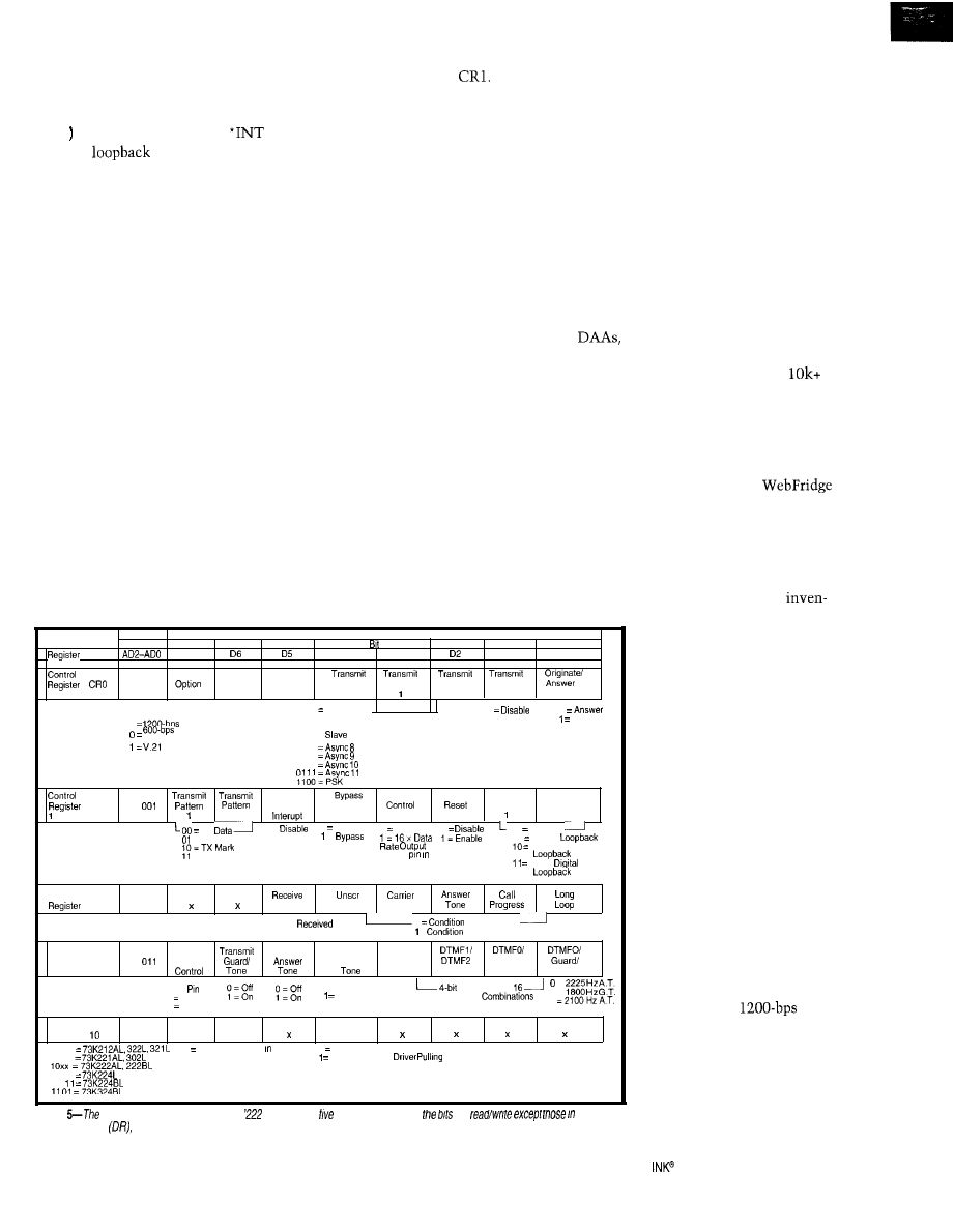
5. Control register 0 (CRO) defines the
basic mode of operation (i.e., modula-
tion standard, answer or originate, and
data format), while Control Register 1
(CR1
configures the CLK and
pins and
modes for testing.
CR1 can also force certain output
patterns (i.e., mark, space, alternate) to
test (also used when modems of differ-
ent types “negotiate”) and bypass the
scrambler, which stuffs the bits neces-
sary to guarantee enough signal activ-
ity for clock recovery at the other end.
CR1 also contains the all-important
RESET bit. TDK points out you can
(and probably should) use it instead of
providing (or relying) on an external
power-up reset circuit.
The Detect Register (DR) gives you
some clue of what’s happening on the
line, including a copy of the RXD bit
so the CPU can monitor incoming data
through the parallel interface. The
other bits detect specific line status
(e.g., unscrambled marks, carrier, an-
swer tone, dial tone, etc.).
The long-loop bit is an indication of
a weak connection likely to experience
errors, so maybe you should hang up
and try again. As mentioned, many of
these lines can assert the l INT output
if so enabled by bit 5 of
The Tone Register (TR) does what it
says. It outputs relevant tones, includ-
ing guard (used in Europe to prevent
bleeding into verboten frequencies],
answer, and DTMF for touch-tone
dialing.
The ID register contains a code so
your firmware can figure out what chip
it’s talking to. Since many K-series
parts share basic features (i.e., register
formats), it’s possible (but not trivial)
to come up with firmware that works
with many chips and standards. The
ID register is also where you twiddle
the *OH (Off-hook) output that con-
nects to the external relay.
It may not take many MIPS to get
the job done, but don’t underestimate
the complexity of dealing with proto-
col. Consider especially the negotiation
phase that takes place when two
un-
like modems try to communicate.
For instance, Figure 6 shows the
V.22 connect sequence, and there’s a
different figure like it for each standard.
And, I haven’t even started talking
about bells and whistles like the ubiq-
uitous AT command set.
Fortunately, TSC offers sample firm-
ware (though only for ‘5 1 family chips)
that can get you off to a running start.
It even includes MNP 4 and 5, which
are popular enhancements for error
correction and data compression.
It all sounds grand, but just keep
some “make versus buy” realities in
mind. If you only need a few-or even
a few dozen-modems, simply head
over to the local PC shack.
If you’re buying a few hundred or
thousand, check out some of the mo-
dem modules on the market. Cermetek,
the source of the mentioned turn-key
offers complete modem mod-
ules as well.
However, if you’re looking at
units, know what you are doing, and
aren’t intimidated by the regulatory
inquisition, TSC may be the way to go.
GO SLOW OR GO BROKE?
Even if you don’t buy the
concept, there’s no shortage of applica-
tions where price is more important
than speed. Like your shopping list,
many day-to-day transactions like
credit-card, automated-teller, and
vending machines; security and
Address
D 7
Data
Number
D4
D3
Dl
DO
Modulation
Transmit
000
0
Mode
Mode
Mode
Mode
Enable
0
3
2
0
0
DPSK
1 =
DPSK
Sell 103 FSK
FSK
0000
PWR Down
0001 = INT Sync
0010 = EXT Sync
0011 =
sync
0100
bits/char
0101
bits/char
0110
bits/char
bits/char
0
0
TXA Output
Originate
1 = Enable
TXA Output
CR1
Enable
CLK
Test
Test
Detect
Scrambler
Mode
Mode
0
0
TX
0 =
0 Normal
0 XTAL
o
00 Normal
= TX Alternate
1 = Enable
=
01 Analog
Scrambler
Remote Digital
= TX Space
at CLK
DPSK Mode Only
Local
Detect
D R
TOW
Control TR
Register
010
Data
Marks
Detect
Outputs
0
not Detected
Datastream
=
Detected
RXD
Transmit
Transmit
output
DTMF
DTMF3
Overspeed
Answer/ Tone
RXD
0 Normal
0 = Data
Code for 1 of
TX DTMF
Dual-tone
=
1 Weak Pull-Up
1
500 Hz G.T.
ID
Register
110
1
0
O H
ooxx
X Undefined. mask software
0 OH Relay Driver Open
Olxx
OH Open Drain
Low
1100
11
Figure
programmer interface to the
consists of regsters. Most of
are
me
Detect Regisfer
which
are
read-on/y.
tory systems; and data log-
gers just don’t call for much
data.
Surprisingly, many of
these applications not only
don’t need a faster modem,
but would be poorly served
by one. For instance, as long
as the telephone company
bills by the minute, the toll
is the same (if your message
is shorter than a few thou-
sand bytes) no matter which
modem you use.
Sometimes, it takes longer
to set up the connection than
transfer the data. Ironically,
due to the simpler negotiation
phase for older standards,
there’s some amount of data
(perhaps at 100 bytes or so)
below which a
transaction completes while
the higher speed modems are
still trying to figure out who
they’re talking to.
The slower modem is also
more robust in the face of
Circuit Cellar
Issue 82 May 1997
83
Calling Modem
Modem
Scrambles
Ones in Low Band
DCD
TD
Ignored
Clamped to
One
Unclamped
Received Data
M o d e m
DSR
DCD CTS
Received Data Output Clamped to
One While
Off
Unclamped Data
Figure
connection handshake for a
(1200 bps) modem takes a
more than a second. Modems that
support
many standards have more complex and time-consuming negotiation phases.
poor line quality, meaning fewer errors
and squint-and-peck keyboard. Any-
and retries. Remember the tortoise and
thing faster is overkill, kind of like
the hare?
filling your fish tank with a firehose.
Priced at only $7.50 in
quanti-
ties, a chip like the ‘222 may be just
what it takes. Why pay for more speed
than you need?
q
Shortly, we’ll see a rash of small and
inexpensive E-mail gizmos in the guise
of phones, organizers, or pagers. What-
ever costumes they wear, it’s for sure
they can’t afford a Pentium, 28.8 mo-
dem, and TCP/IP stack.
In fact, 1200 bps is just about right
for something with a 4 x
16
display
Tom
has
been working
on
chip, board, and systems design and
marketing in Silicon Valley for more
than ten years. He may be reached by
E-mail at
by telephone at (510)
or by
fax at (510)
K-series modem chips
TDK Semiconductor Corp.
1435
1
Rd.
Tustin, CA 92780-7068
(714) 508-8800
Fax: (714) 508-8877
www.tsc.tdk.com
modem modules
Cermetek Microelectronics
406 Tasman Dr.
Sunnyvale, CA 94089
(408)
Fax: (408)
www.cermetek.com
425 Very Useful
426 Moderately Useful
427 Not Useful
Just connect a keyboard,
monitor/LCD, a disk drive
your ready to run. Or
Forget the drive and boot
directly from a Flash disk.
PC/ 104 Modules for
Fax/Modem, SCSI, Ethernet,
for Point
Of Sale and Web
Browsers/Servers. Prices start at $200.00
1
*Wide CPU Selection:
DX4, 586, Pentium.
All
have Real Time Clock, Serial, Parallel, IDE, and Floppy.
On
Board Watchdog Timer.
BIOS with Power Saving Green Mode.
*Wide Bus
104, ISA, PCI.
10.4”
super bright LCD Panel Kits.
Hardware and Cable kits included for most boards
618-529-4525 Fax 457-0110
529-5708
11
EMAC WAY, CARBONDALE, IL 62901
WORLD WIDE WEB:
REMOTE POWER CARD!
O E M
a
CHAN
STEREO
2 CHAN DAC
5 YEAR LIMITED WARRANTY
F R E E S H I P P I N G I N U S A
8 4
Issue May 1997
Circuit Cellar INK@
The Circuit Cellar BBS
bps
24 hours/7 days a week
(860) 871-l 988-Four incoming lines
Internet:
The Circuit Cellar BBS Joins the Big League
What do you suppose is one of the most common questions I’ve been
asked via E-mail over the last year or two? “Can access the
using the
Internet?” The answer has a/ways been no-until now.
After months of research, experimenting, and procuring, I’ve finally
brought the Circuit Cellar BBS to the
Let me my original goals:
Multiple simultaneous users
for a dial-up interface so people can continue to
the modem
lines directly
l
any desktop platform and operating system dial in to the system
E-mail for in-house staff and users
l
Access to messages and files from the
using either telnet, or
the Web
Ability host our Web sites
l
LAN connections for in-house staff
The ultimate solution that me achieve my goals turned out to be
the Wildcat!
Network
from Mustang Software.
Now that the new system is on-line, give you a brief
of what if
offers and how to access it.
Features
The Circuit Cellar BBS continues to offer the same basic
features that we’ve supported for the past 10 years-direct
access to Circuit Cellar staff and other callers using public
and private messages, and access to files related both to past
Circuit Cellar articles and to computers and electronics in
general. We also offer information about
Circuit Cellar INK
such as how to subscribe, get back issues, or write articles;
upcoming editorial events and features; and other Circuit
Cellar products.
What’s new is how the information can be accessed. As
I’ve mentioned, your options are dial-up, telnet, ftp, and Web.
Dial-up
Calling (860) 871-1988 connects you to a modem that
leads into the text-based version of the BBS. ANSI menus
continue to be supported, as does flat ASCII for those of you
with dumb terminals. I’ve tried to keep the menu, message
area, and file area structures as close as possible to the old
system, so veteran callers shouldn’t have much trouble
navigating.
Those of you whose only exposure to the Internet is Web
browsing may not be familiar with telnet, a text-based trans-
port protocol that remotely accesses hosts across the Inter-
net. When you run a telnet client on your local system and
give it the Circuit Cellar BBS net address, you immediately
connect to the text-based version of the system exactly as if
you’d dialed into one of the modems. The biggest difference
is the lack of long-distance phone charges. Internet users in
Australia can use the BBS as easily and inexpensively’as
those across the street.
You need an Internet connection and a telnet client.
Windows 95 and NT have simple ones, and they are readily
available for other platforms. Many newer
programs
also come with telnet support (e.g., Qmodem Pro from Mus-
tang and Procomm Plus from Quarterdeck). While I try to
get the name server straightened out at our ISP, you may
telnet directly to our IP address (206.119.19.172). Eventu-
ally, you’ll access
to get in.
Most Internet users have used ftp (file transfer protocol)
before. Obviously, it transfers files from machine to machine
across the Internet. While we’ve had a minimal ftp site for
some time now, it’s only had recent article-related files
available on it.
We now have all the files from the BBS available via ftp.
Point your ftp client or Web browser at
to see what we have to offer.
Web
Perhaps the most exciting new access method is your
trusty Web browser. Access all the public messages, your
own E-mail, and all the file areas without leaving the com-
fort of your favorite browser. We do require your browser to
support frames (Microsoft Internet Explorer or
Navigator), but that covers most of the world.
When you first connect to our Web address at
you’re asked whether you want to
access one of our Web sites or the BBS. When you select the
BBS, you’ll be asked for a user name and password. Enter
the information you use to log onto the BBS. New users can
also sign up for access.
Once in, check messages, see who else is on, modify user
settings, answer questionnaires, and download files.
Join Us
I’ve been extolling the virtues of the Circuit Cellar BBS
for years here in these pages. If the cost of the phone call
has kept you from joining us, I encourage you to jump right
in. Chances are, you’ll either learn something new, teach
someone else something new, or both.
Circuit Cellar INK@
Issue 82
May 1997
85
INTERRUPT
Processing-A Matter of Definition
you might have guessed, the real Circuit Cellar is underground. Well, not really-it’s the bottom floor of the
and like a raised ranch, only one end of the house is at ground level. In my case, having ground-level.
access is moot. I still can’t see what’s going on outside unless I look at a closed-circuit TV monitor. It’s an insulated
reality.
Last night, I sat down at my computer and proceeded to judiciously pen an eloquent dissertation on the relative comparisons of
various embedded-processor architectures. One eye was on the word-processor screen, the other on the howling April 1st blizzard with
winds outside. The businessman/publisher side of me considered, “Let’s get this over with fast, write the editorial, and get the
magazine to press.” On the other hand, the untamed/experimenter side of me mused, “Oh boy, disaster time again. Let’s see if all these
back-up systems really work.”
Let’s face it. Connecticut isn’t exactly wilderness. It’s just a matter of what you consider normal. When Atlanta gets 2” of snow, the
whole city shuts down. People down Maine (as they call it) think 2’ is nothing.
Unfortunately, the definition of “normal” in Connecticut is a moving target. You might as well use a dartboard to predict the weather
around here. Oklahoma may be tornado alley, but if memory
me correctly, two of the three worst tornadoes in U.S. history were in
Connecticut.
The good news is that we’re a rich state and close to everything. The bad news is that we’re a rich state and close to everything.
When that one tornado touches down every couple of years, it can’t help but land on something expensive. When that thunderstorm rips
through the state on a hot August afternoon, every lightning bolt strikes a real target.
After about two hours of retyping the same sentence innumerable ways, attention to the blizzard won out. If it weren’t for the
generator and E-mail, I could have hoped that being snowbound and without power might afford yet another excuse for a late editorial.
The morning proved to be everything that the night predicted. Up to 2’ of heavy snow certainly was not something I considered
normal. But, it was normal to consider that it would inevitably happen. This stuff was so heavy that opening the front door was impossible.
I opened the garage door and my Westie,
went bounding out into the snow. About 5’ out, she suddenly realized dogs with 6” of
ground clearance don’t do well in deep snow. I trudged out and rescued her.
That should have been a message. You know-something like “where dogs fail to tread.” While I pride myself on being ready for
practically anything, the reality of having to use it all suggests that I might have a little too much wilderness in my urban lifestyle.
The solution was anything but easy. It was one of those situations where you needed everything just to use one thing. Yeah, I knbw
it sounds stupid, but you had to be there.
Our driveway is about 600’ long. Usually, I plow it with a light pickup truck. opened the door in front of the truck, jammed it into
4WD low, dropped the plow, and got about Undaunted, I went to the next garage door, fired up the
snow blower and proceeded
to clear a path for the plow. That went about 20’ before the heavy wet snow made using it an equal aggravation. The third garage door
offered the final confidence that machine could ultimately prevail. I climbed up on the tractor and fired up the diesel engine. Here was,
using a tractor to dig out the snow blower to dig out the truck to dig out.... You get the picture.
Well, I guess I won’t be discussing bits as they apply to embedded processors this time. Believe or not, it’s possible to get a
tractor stuck in 2’ of snow. Now I’m down to using a shovel to dig out the tractor to dig out, etc., etc. I didn’t lie when I told Janice that my
editorial was related to the magazine focus. Using a shovel is after all, processing snow-a bit at a time.
96
Issue 82 May 1997
Circuit Cellar
Wyszukiwarka
Podobne podstrony:
circuit cellar2001 05
circuit cellar2000 05
circuit cellar2002 05
circuit cellar1994 05
circuit cellar1993 05
circuit cellar2004 05
circuit cellar2003 05
circuit cellar1995 05
circuit cellar1996 05
circuit cellar2001 05
circuit cellar1997 05
circuit cellar1993 05
circuit cellar1996 05
circuit cellar2001 05
circuit cellar1995 05
circuit cellar1994 05
circuit cellar2003 05
więcej podobnych podstron