INK
A Match Made in Heaven
ow
perfect a marriage of graphics and video:
closed caption decoding and display. Pioneered by
the public broadcasting system, closed captioning has
been growing in popularity in recent years. In fact, this
system that aids people with hearing impairments enjoy television with the
rest of us has become so prolific that Congress has mandated that, as of
July 1993, all television sets sold in the US. with screen sizes 13” and
bigger must include closed caption decoding circuitry.
After having a chance to experiment with the Vertical Blanking Interval
Explorer project that won second place in our last Circuit Cellar Design
Contest, have seen first hand just how much of today’s television
programming already includes closed caption information. If you buy a new
TV in the next few months, you, too, will be able to see how useful a system
it really is.
Motorola has taken a giant step in helping manufacturers include
closed caption decoding in future televisions at minimal additional cost.
Almost all of today’s larger televisions already include a microcontroller and
on-screen character display. The new
microcontroller also adds
caption decoding and, with minimal additional components, directly drives
the red, green, and blue CRT guns with superimposed captions. Be sure to
check out our first feature article that describes the chip’s design and use.
Next, when rendering three-dimensional graphics on a two-dimensional
display device, a fundamental understanding of vector and matrix mathemat-
ics is crucial. Find out what’s involved with such math and how to do it.
In our final feature article, David Erickson combines custom chip
design with an off-the-shelf LCD display to off-load much of the graphics
processing from the microcontroller to the display controller. You, too, can
make a chip.
In this month’s embedded ‘386SX installment, Ed adds some timers to
the system as he continues to lay the foundation for his system. Jeff does
some hands-on testing of the myriad kinds of batteries found on the market
today and makes some suggestions for which kinds are best used in what
applications.
Tom goes over the details of Sony’s exciting new Mini Disc. Not only
does this system promise to replace traditional cassettes, but it should be a
boon for computer mass storage and archival. John takes a look at
Signetics’
bus and its usefulness in embedded systems. Finally, Russ
covers patents dealing with this issue’s graphics and video theme.
CIRCUIT CELLAR
THE COMPUTER
APPLICATIONS
JOURNAL
FOUNDER/EDITORIAL DIRECTOR
PUBLISHER
Steve Ciarcia
Daniel Rodrigues
EDITOR-IN-CHIEF
Ken Davidson
PUBLISHER’S ASSISTANT
Susan McGill
TECHNICAL EDITOR
Michael Swartzendruber
CIRCULATION COORDINATOR
Rose
ASSOCIATE EDITOR
Robert Rojas
CIRCULATION ASSISTANT
Barbara
ENGINEERING STAFF
Jeff Bachiochi Ed Nisley
CIRCULATION CONSULTANT
Gregory Spitzfaden
WEST COAST EDITOR
Tom
Cantrell
CONTRIBUTING EDITORS
John Dybowski Russ Reiss
BUSINESS MANAGER
Jeannette Walters
ADVERTISING COORDINATOR
Dan Gorsky
NEW PRODUCTS EDITOR
Harv Weiner
ART DIRECTOR
Lisa Ferry
GRAPHIC ARTIST
Joseph Quinlan
CONTRIBUTORS:
Jon Elson
Tim
Frank Kuechmann
Pellervo Kaskinen
CIRCUIT CELLAR INK. THE COMPUTER APPLICA-
TIONS JOURNAL
is published
monthly by
Cellar Incorporated. 4 Park Street,
20, Vernon, CT 06066
Second
Vernon.
One year (12
U.S.A. and
$43 35 All
orders payable U.S.
only.
postal money order
check drawn on U.S. bank.
orders
and
related questions to The Computer
Journal
P 0 Box 7694,
NJ 08077 or call (609)
POSTMASTER. Please send
changes The
Computer
Journal.
P 0
Box 7694,
NJ 08077
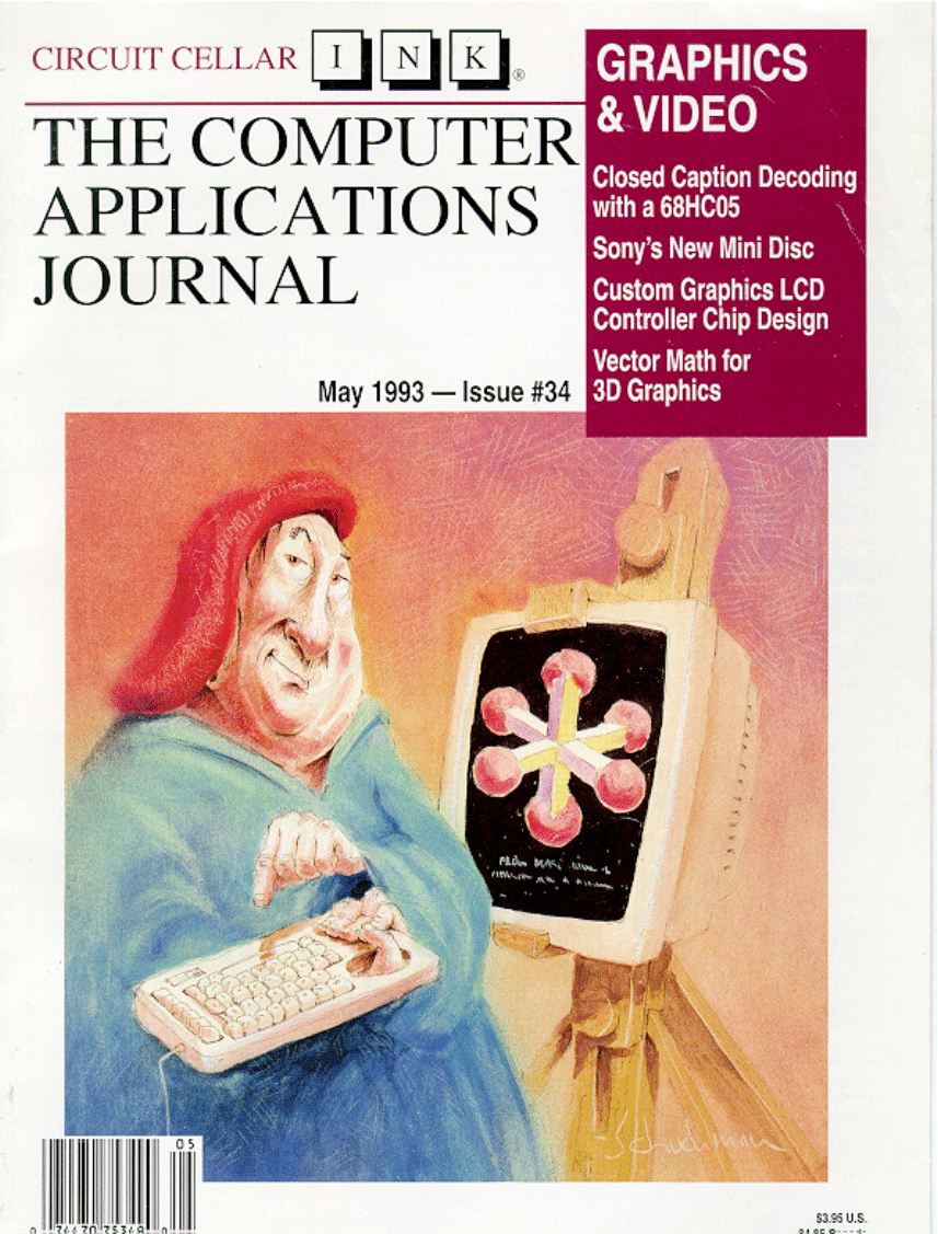
Cover Illustration by Bob Schuchman
PRINTED IN THE UNITED STATES
ASSOCIATES
NORTHEAST
Debra Andersen
(617)
Fax: (617) 769-8982
MID-ATLANTIC
Barbara Best
(908)
Fax: (908) 741-6823
NATIONAL ADVERTISING REPRESENTATIVES
SOUTHEAST
Collins
WEST COAST
Barbara Jones
(305) 966-3939
Fax: (305) 985-8457
MIDWEST
Nanette Traetow
(708) 789-3080
Fax: (708)
Shelley Rainey
(714)
Fax: (714)
Hrs 300112001240019600114
stop
9600 bps Courier HST, (203)
All programs and
Circuit
been carefully
to ensure
performance
transfer by subscribers.
no
no
or liability of any
these
programs
or the consequences of any such errors Furthermore, because of possible
in
and
of
and
of reader-assembled
INK
any
the safe and proper
of reader assembled
based
or from
plans,
or
Cellar INK.
contents
1993 by
Cellar Incorporated All
reserved
of
whole
consent from Circuit Cellar Inc.
2
Issue
May 1993
The Computer Applications Journal
CLOSED CAPTIONING
the
MOTOROLA
by Janice Benzel Linda Reuter Nuckolls
Vector Approach Simplifies
THREE-DIMENSIONAL GRAPHICS
by Fred H.
GRAPHICS LCD
Control for
Embedded Applications
by David Erickson
Editor’s INK/Ken Davidson
A Match Made in Heaven
New Product News
edited by Harv Weiner
Firmware Furnace/Ed Nisley
Time: The ‘386SX Project Gains a Timer
From the Bench/Jeff Bachiochi
Squeeze That Battery ‘Till It’s Dry
Silicon Update/Tom Cantrell
Audio Rx-Skippy CDs? Tangled Tapes?
Call an MD...
Embedded Techniques/John Dybowski
Interchip Traffic
Patent Talk/Russ Reiss
from the Circuit Cellar BBS
conducted by Ken Davidson
Steve’s Own INK/Steve Ciarcia
The Club
Advertiser’s Index
The Computer Applications Journal
Issue May1993
3
Edited by Harv Weiner
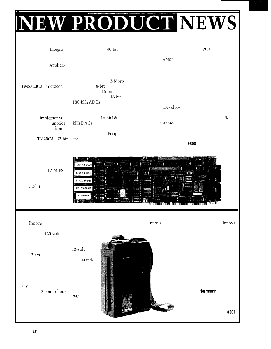
HIGH-PERFORMANCE APPLICATION COPROCESSOR
Innovative
RAM/ROM, and a
Software is developed
control;
nonlinear
tion has introduced a
single-cycle floating-point
and tested using the
control; audio digitizing,
high-performance IBM
multiplier/accumulator.
optimizing 100%
processing, and playback;
PC/AT plug-in
Additionally, the full-length
compatible C compiler or
digital filters; math
tion Coprocessor board.
IBM plug-in card features an
incremental Forth compiler.
coprocessing; and image
The PC31 combines the
eight-channel prioritized
Applications are quickly
processing.
Texas Instruments
interrupt controller,
developed and tested using
The PC3 1 sells for
1
DUART, six
digital
the comprehensive integer
$850 in single quantities
troller and the ANSI C or
I/O ports, three
and floating-point math,
and complete develop-
the Forth programming
counter/timers, two
analog and digital I/O, and
ment packages start at
languages to provide a
(one of
video display libraries
$2995.
complete integrated
which is 8: 1 multiplexed
provided with the
solution to the develop-
into a programmable-gain
ers Package. All system and
Innovative Integration
ment and
amp), and four
application procedures may
4086 Little Hollow
tion of real-time
Up to 16
conveniently be
Moorpark, CA 93021
tions and IBM PC
megawords of 0-7-wait-state
tively edited, tested, and
(805) 529-7570
end signal processing.
RAM is supported.
executed at full machine
Fax: (805) 529-7932
The
1
cards addressing large
speed.
architecture is optimized
data gathering and audio
Applications for the
for computationally
applications are available.
board include real-time
intensive floating-point
digital signal processing
algorithms and operates
at a sustained
33-MFLOPS throughput.
The processor provides
two
counter/
timers, seven prioritized
interrupts, two synchro-
nous serial ports, on-chip
AC POWER SOURCE
Electronics has introduced the AC Power
Pack, a portable, rechargeable power source specially
designed for
AC/DC products up to
SO watts. The AC Power Pack provides an
alternative to traditional portable power
sources and combines both
DC
and
AC capability. In addition,
the Power Pack has a removable,
alone AC module that can be used to
provide 120-volt AC power from any car
cigarette lighter socket.
The entire unit measures 3” x 3”
x
lighter while the engine is running or in four to six hours
using the
AC Charger. Also available from
is a Solar Charger that will recharge the AC Power Pack
in under six hours on a sunny day.
For protection against overloading and
damaging circuits, the AC Power Pack
features a built-in regulator that prevents
overcharging. The unit can be recharged
up to 1000 times on its replaceable,
maintenance-free, sealed lead-acid battery.
The AC Power Pack sells for $175 and
is covered by a one-year warranty.
weighs only three pounds, and
lnnova Electronics Corp.
contains a
battery. The AC
17287
Mount
St.
inverter module measures I
x 3” x
Fountain Valley, CA 92708
7.5”
and weighs 0.75 pounds. The AC
(714) 432-1184
Power Pack is easily recharged in one to
Fax: (714) 432-7910
three hours through any vehicle cigarette
6
Issue May
1993
The Computer Applications Journal
NEWS
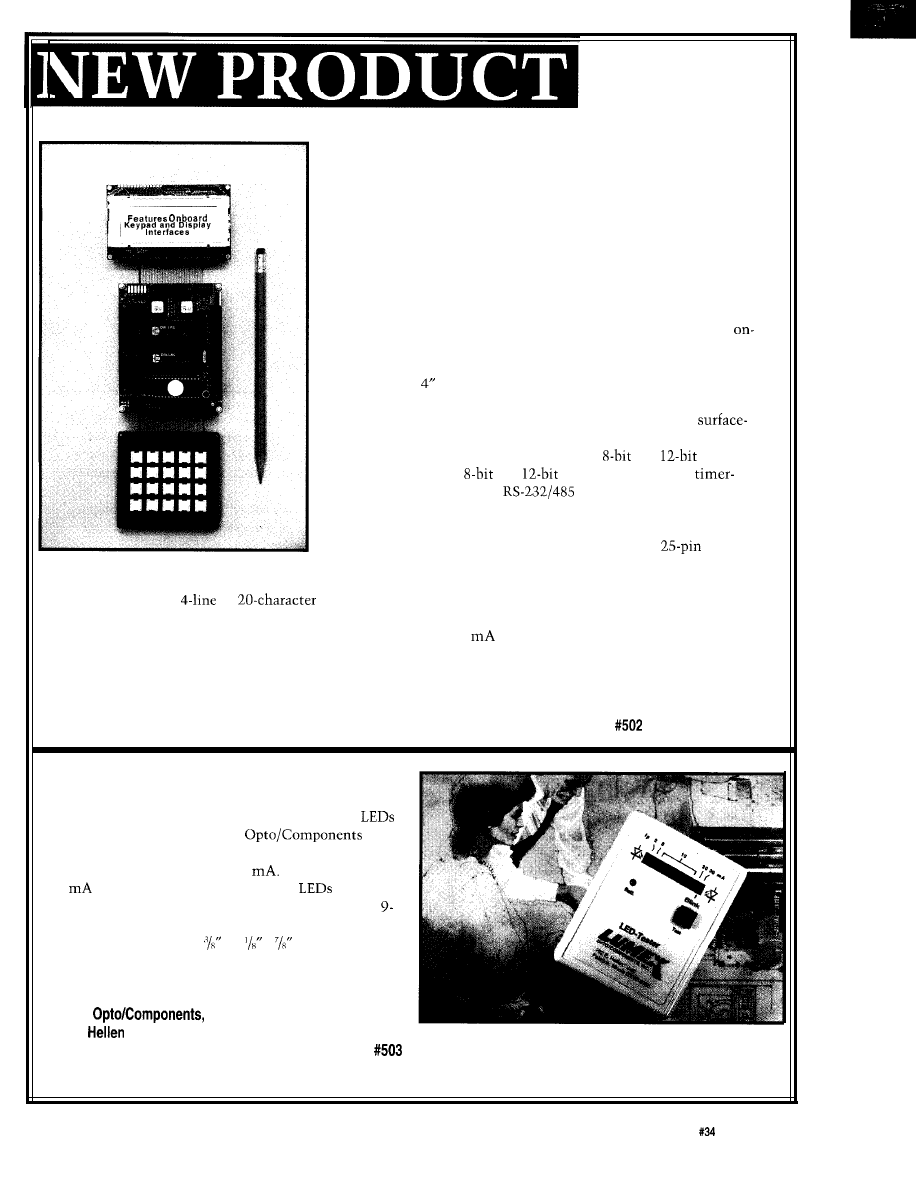
The QED Board
INSTRUMENT DEVELOPMENT SYSTEM
The QED Product Design Kit from Mosaic Industries is a “generic
instrument” that speeds development of instrumentation and control
applications. Programmable from any PC or terminal, the kit integrates
a 68HC
11
-based controller board, LCD display, keypad, power supply,
and prototyping board in an aluminum instrument enclosure.
The heart of the instrument kit is the QED Board, an embedded
computer that hosts a resident high-level Forth programming environ-
ment in on-board ROM. Interactive debugging tools support breakpoint
insertion, tracing, and single stepping. A built-in multitasking execu-
tive implements cooperative and time-sliced task switching, and
board libraries include I/O device drivers as well as floating point,
calibration, and matrix math functions.
The 3.2” x board hosts up to 384K of memory including battery
backed write-protectable RAM that eliminates the need for PROM
burning while programming. Fabricated using double-sided
mount technology, the battery-operable board provides keypad and
display interfaces, digital I/O, up to sixteen
and
ADC
channels, up to eight
and
DAC channels, eight
controlled signals, and dual
serial ports.
An aluminum instrument enclosure houses all of the hardware. In
addition to the installed QED board and prototyping board, there is
room for two additional 3.2” x 4” circuit boards. Two
serial
of the enclosure.
communications connectors and a power jack reside on the back panel
The display is a
by
high-contrast liquid crystal display with a visible display area of
1” x 3”.
The keypad features 4 rows by 5 columns and is 2.7” x 3”. Custom labels can be inserted under the clear plastic key
caps. A wall-mount DC power supply provides 6 VDC at up to 500
through a jack on the back panel of the
enclosure.
The QED Product Design Kit is priced from $875 and the QED board is priced from $495.
Mosaic Industries, Inc.
5437 Central Ave., Ste. 1
l
Newark, CA 94560
l
(510) 790-1255
l
Fax: (510) 790-0925
LOW-COST LED TESTER
A compact, hand-held unit for convenient testing,
evaluation, and quality control checks of discrete
has been introduced by Lumex
Inc.
The LED Tester features single sockets with fixed
current levels of 2, 5, 20, and 30
Seven sockets at
10
are also provided so that similar
can be
easily compared for color and/or brightness. A single
volt battery powers the tester.
The LED Tester is 2
x 3 x and weighs 3
ounces, complete with battery.
The LED Tester sells for $38.00 including battery.
Lumex
Inc.
292 E.
Road
l
Palatine, IL 60067
(708) 359-2790
l
Fax: (708) 359-8904
The Computer Applications Journal
Issue
May 1993
7
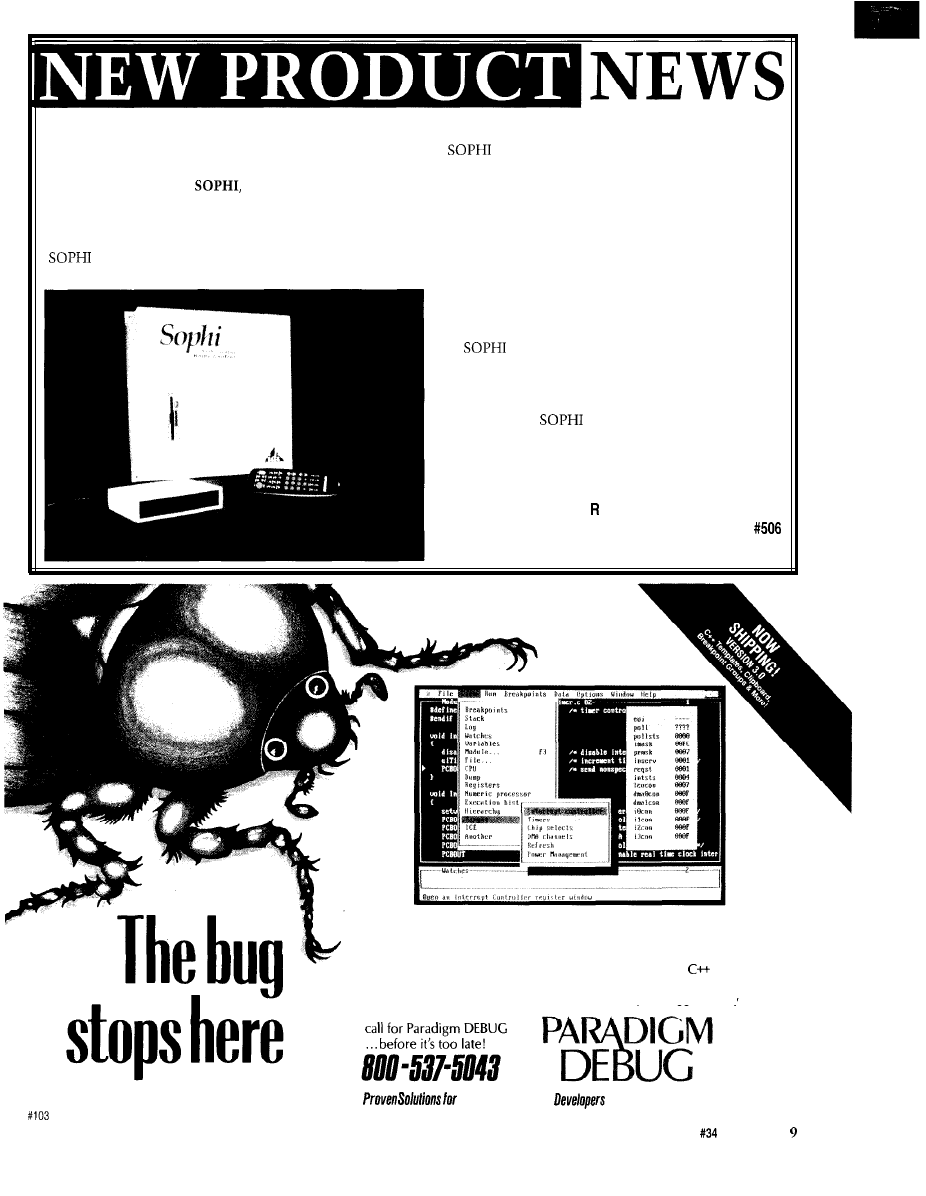
DEBUGGING TOOL FOR ROM-BASED SYSTEMS
Rhombus Design’s romTRACKER debugging tool is
designed specifically for ROM-based systems. It mea-
2” x is PLD based, and installs directly between
the ROM and its socket. All of its functions are available
while running out of ROM, and include tracing the
execution of segments of code, locating the addresses of a
hung program, and producing a hardware trigger on any
ROM address.
The romTRACKER is self-contained with its own
Start Trace address selection. The addresses that execute
in the selected segment are stored and mapped onto an
array of 16
When operating at one address per
LED, the resulting coverage of 16 consecutive addresses
is quite adequate to show the details of how conditional
code is executed. For each segment selected, correlating
the operation of a ROM emulator, supporting the
the address-mapped
with the addresses in the
transition from RAM-based development to ROM
program listing is quick and simple. Other modes allow
production, use as the sole debug tool in combination
expanded coverage. There are no cables to load or
with an EPROM programmer, and use as a portable tool
influence the target signals, it operates with any
on-site.
sor that uses a 28-pin DIP EPROM, and it takes its power
The romTRACKER sells for $129 and is supplied
(up to SO
from the socket.
with a shirt-pocket-size protective case.
The universal operation and pocket size of
romTRACKER will allow it to contribute to the user’s
Rhombus Designs, Inc.
debugging process regardless of the processor type and
5
Woodlawn Green
l
Charlotte, NC 28217
existing tools. Typical uses will include complementing
(704) 525-3351
LOW-LEVEL MEASUREMENTS HANDBOOK
Keithley Instruments has published a
handbook on making low-level measurements. The “Low-Level
Measurements Handbook” is written both for the measurements expert and novice, with details on specific tech-
niques for making even the most difficult and sensitive measurements.
Illustrations and schematics accompany the measurements tutorials.
The updated handbook covers essential techniques for improving
measurement accuracy, including sections on common low-level
voltage, current, and resistance measurement techniques; typical
applications; error sources and how to avoid them; and an instrument
selector guide.
The handbook includes an introductory section that explains why
special instrumentation is often required when making low-level
measurements, along with specifications and circuitry to look for when
buying instrumentation that will distinguish low-level from
purpose instrumentation.
Step-by-step procedures and instructions are provided to the reader.
Also included is a detailed glossary of terms.
For a free copy of the handbook, contact:
Keithley Instruments, Inc.
28775 Aurora Rd.
Cleveland, OH 44139
(216)
Fax: (216) 248-6168
Issue
May 1993
The Computer Applications Journal
HOME CONTROL SYSTEM
Digital Technology has introduced a Sophisticated
Home Control System,
that provides complete
control of security, environment, lighting, appliances,
and telephone functions. The system is easily installed
in existing homes and extremely simple to operate.
is unique because it incorporates all of these
features into one system.
is connected to the existing cable TV wiring
in a home and displays its status on an unused cable
channel. It is controlled by a hand-held remote that also
controls the TV, VCR, and audio system, or by any
telephone in or out of the home. The TV screen displays
a series of easily understood menus and the user is guided
by a series of voice prompts.
The security system uses wired or wireless sensors,
such as door and window sensors, fire and smoke
sensors, and motion sensors. The unit can dial any
telephone number and deliver prerecorded messages.
provides multizone heating and air condi-
tioning capability. The basic system will control up to
four zones. Temperature changes are made with the
hand-held remote through the TV screen.
In addition,
includes a voice mail and call
forwarding system and X-10 technology, which is used
to control up to 256 lamps and electrical appliances.
Digital Technology, Inc.
1000 Riverbend Blvd., Ste.
l
St. Rose, LA 70087
(504) 467-i 466
l
Fax: (504) 467-2146
And the headaches, cold sweats and other symptoms associated
with debugging real-time embedded applications. Paradigm
DEBUG offers you choices:
l
Intel or NEC microprocessors
l
Remote target or in-circuit emulator support
l
C,
and
assembler debugging
l
Borland, Microsoft and Intel compatibility.
Kickstart your embedded system with the only debugger family
to have it all. Give us a
Embedded C/c++
P A
R
A D
IGM: (607) 748-5966
FAX: (607) 748-5968
The Computer Applications Journal
Issue
May 1993
A new software program that converts an IBM-compatible computer into a fully functional logic analyzer has
introduced by Logixell Electronics. With the
Real Logic Analyzer,
up to
five waveforms can be monitored
hrough the standard PC parallel printer port. The user connects a circuit to the port by making a simple cable or
using Logixell’s optional cable with universal test clips.
The software uses the computer’s memory to
capture 64K samples of data as fast as every 1.2
(depending on computer). Full triggering capabilities
allow for the trigger word to be set to any combination
of High, Low, or Don’t Care values. The trigger point
may be set anywhere within the 64K buffer to allow for
capturing of both pre- and post- trigger waveforms.
Captured waveforms are displayed graphically on the
computer screen and can be viewed at several different
zoom levels. A continuous display mode allows for an
oscilloscope-type of real-time display.
The Real Logic Analyzer comes with a 32-page
instruction manual and program diskette for only $35.
The optional Test Cable sells for $17.95.
Logixell Electronics
Ml 1-2881 Richmond Rd.
l
Ottawa, Ont.
Canada
(613) 828-4159
l
Fax: (613) 828-8954
Schematic Capture
to Error-free PCB
and
are
“personal use” versions of and compat-
ible with our professional level
PRO
PCB Design System.
These programs are perfect for design engineers who desire an economi-
cal yet powerful
desi program.
checker and a
The complete system includes the
to view gerber plot files. The schematic
capture module supports A through E size sheets, comes with user
expandable library and outputs
The PCB Layout module
supports layers, trace width from 0.001 inch to 0.255 inch, flexible grid,
accepts
from several different formats such as
and
SMD
penplotters, gerber p
nenk on both sides of the board and outputs to
and dot matrix printers.
For a FREE Evaluation call l-800-972-3733
30 DAY
MONEY BACK GUARANTEE
3rd St, Suite B-8,
Pompano
Beach, FL
FAX
Single Board Computer
More Power, Superior performance,
That Meets Above Average Industry
Has Unequal Technical
Support And, Oh,Yeah, It’s Cheaper.
2
serial
ports
3
programmable parallel
ports
2
configurable memory sockets
detect interrupt and reset
counter-timers
watch dog timer
expansion connector
Only $159.00
ALSO AVAILABLE:
MMT-196,
MMT-EXP
In
fact,
you’ll get the best product for about
half the price. If you’re interested in getting the
most out of your project, put the most into it.
For the least amount of money. Call us today
for complete data sheets, CPU options, prices
and availability.
Midwest Micro
2308
East Sixth Street, Brookings, SD 57006
Fax
10
Issue
May 1993
The Computer
Journal
I
I
ARBITRARY WAVEFORM GENERATOR
Real Time Devices has announced the FG102, a
low-cost PC-bus arbitrary waveform generator. The
unique design of the FG102 uses the host computer’s
DMA and interrupt circuitry to transfer data, enabling
it to generate extremely long waveforms. Two
analog waveforms can be generated simultaneously as a
DMA-controlled background task. The waveforms can
be generated by the mathematical functions in any
high-level language or by an application program.
Alternatively, the waveforms can be digitized
world signals acquired from a data acquisition system
and reproduced by the FG 102.
In contrast to RAM-based arbitrary waveform
generators, the
use of DMA and interrupts
permits much larger files to be used. The waveform
size is limited only by the amount of available hard
disk space, since the FG102 uses a buffer swapping
software technique to overcome
64K page
barrier. This allows waveforms larger than 64K to be
generated in real time.
The waveform data transfer rate is programmable;
the maximum rate depends on the host computer. Data
transfer rates on an
machine are in excess of
100,000 points per second. The FG102 supports single
and repetitive waveform generation and either DMA or
non-DMA transfer modes. The buffered analog outputs
have a
settling time and four jumper-selectable
output voltage ranges. The output waveform can be
to an on-board audio amplifier to directly drive
an
speaker.
Applications for the FG102 include automated
testing, acoustics, DSP, speech synthesis, or any applica-
tion requiring computer generation of large arbitrary
waveforms.
Software support for the FG102 includes program-
ming examples in
Turbo C, and Turbo
Pascal. A diagnostic program is included to verify the
operation and configuration.
The FG102 Arbitrary Waveform Generator sells for
$459.
Real Time Devices, Inc.
820 N. University Dr.
l
P.O. Box 906
State College, PA 16804-0906
(814) 234-8087
l
Fax: (814) 234-5218
The BCC52 Computer/Controller Micromint’s
selling stand-alone single-board
Its cost-effective architecture needs only a
supply and terminal to become a complete
or end-use system, programmable in
The BCC52
sockets for up to
of RAM/EPROM, an “intelligent” 27641128
EPROM programmer, three parallel ports, a serial
terminal
with auto baud rate
a serial
port. and bus-compatible with the full line of
expansion boards
full floating-point BASIC is fast and
for the most complicated tasks, while its cost-effective
allows it to be
for many new areas of implementation. It can be used both for development
end-use
PROCESSOR
CMOS
RS-232
*lumper-selectable
to
AS-232
programmable
bytes ROM (full BASIC Interpreter)
parallel ports
a 8255 PPI
bytes RAM
console
*three
*five on-board sockets
to
6264
RAM
an 2764 or
27126 EPROM
L
B C C 5 2
BASIC-52
RAM
99.00
$ 1 5 9 . 0 0
range
$ 2 9 4 . 0 0
$ 2 2 0 . 0 0
BCC 5 2CX
CMOS
5 2 5 9 . 0 0
$159.00
l
New C Programmable miniature controller
l
Seven 1 O-bit analog inputs
l
Seven digital inputs
l
1 O-bit DAC: voltage or current output
l
Twelve digital/relay driver outputs
l
serial ports
l
Enclosure with LCD/Keypad available
l
Expansion bus for additional, low cost
l
Easy to use
Dynamic
development software
only
Z-World Engineering
1724 Picasso Ave., Davis, CA
(916)
757-3737
Fax: (916)
24 hr. Information Service: (916) 753-0618
(Call from your
fax
and request data sheet
The Computer Applications Journal
Issue
May
1993
11
URES
Closed Captioning With
The Motorola
Vector Approach Simplifies
3-Dimensional Graphics
Graphics LCD Control For
Embedded Applications
Closed
Captioning
With The
Motorola
Janice Benzel
Linda Reuter Nuckolls
0
he next TV you
purchase will most
likely have built-in
closed-caption capability,
thanks to the Television Decoder
Circuitry Act of 1990. Congress
enacted this law to eliminate the need
for consumers to purchase expensive
add-on decoder hardware to view the
captions that are included in television
broadcast signals. By July 1, 1993,
televisions with screens
(or greater)
in size sold in the U.S. must be able to
decode and display closed captions.
The benefits of this law will be
widespread. For 23 million hearing
impaired Americans, the Television
Decoder Circuitry Act means in-
creased access to captioning at home
and in public facilities. In addition,
extended data services, to be transmit-
ted in the caption format, will provide
new features with universal appeal.
These services could include program
information or captions in a second
language or at another reading level.
The Decoder Act forced television
manufacturers into a race to define a
closed-caption standard and incorpo-
rate it into the 6-billion-dollar U.S. TV
market. The manufacturers have kept
one eye on the calendar and the other
focused on cost issues. Semiconductor
suppliers have hastily designed parts
for the closed-caption niche, but most
of the multichip sets or specialized
they offer require external controllers.
The need for multiple
increases
system complexity and cost.
A SINGLE-CHIP SOLUTION
The Motorola
is a
true single-chip solution, since it
12
Issue
May 1993
The Computer Applications Journal
Chrominance
Luminance
r
Horizontal Sync Pulses
63.4 microseconds
NTSC Video line
Vertical Sync Pulses
1-9
11 12 13 14 15 16 17 19 20 22 23
262 263
Vertical blanking interval
16.7 milliseconds
NTSC Video Field
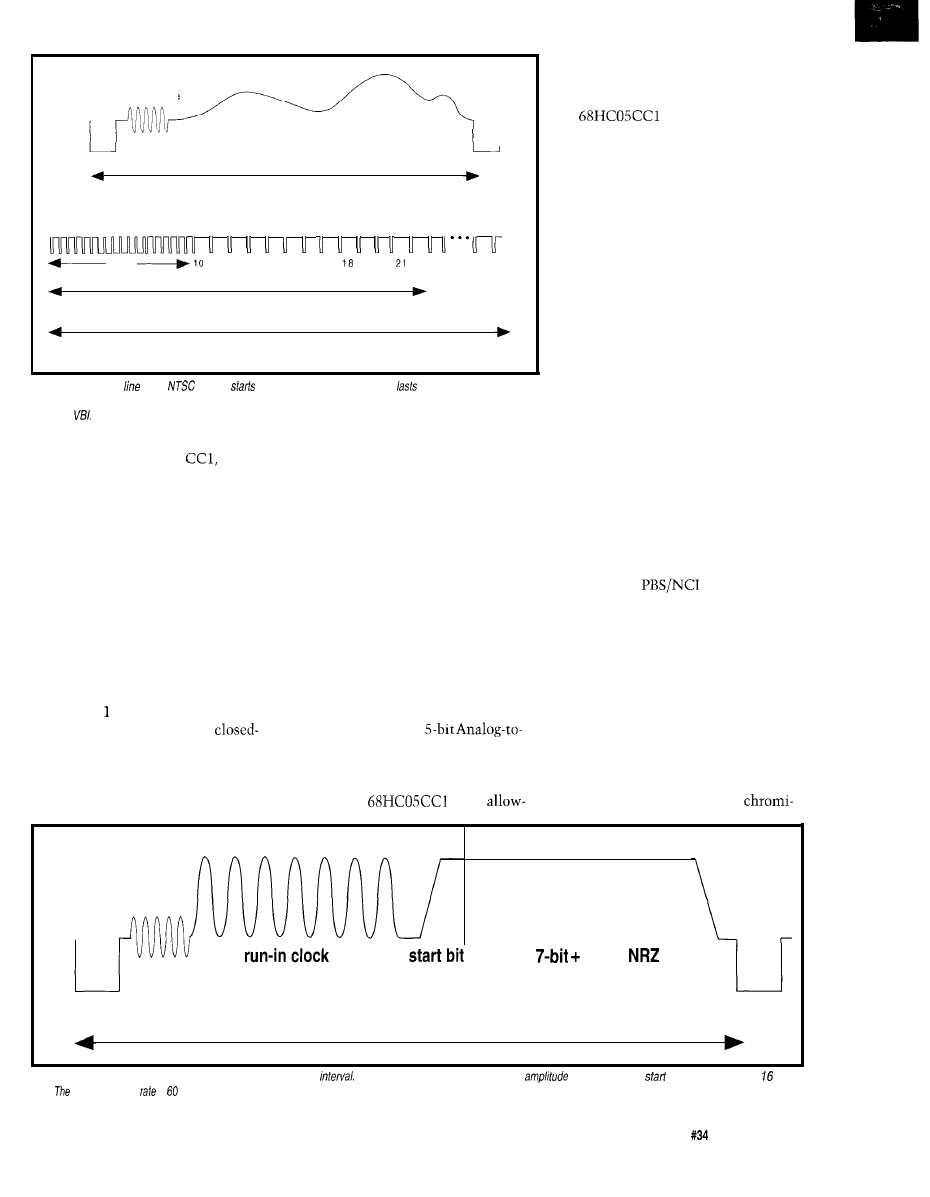
Figure l--Each scan
of an
picture
with a horizontal sync pulse and
63.4 microseconds. Each
field, made up of262.5 scan lines, starts with an invisible vertical blanking interval. Caption data is embedded in line
21 of the
combines the controller and caption
systems on one die. The
an
offspring of the Motorola “T” series of
TV microcontrollers, was developed by
Motorola in partnership with Thom-
son Consumer Electronics. The 6805
based microcontroller includes
peripherals used for basic TV control
with special hardware and software for
the decoding and display of closed
captions.
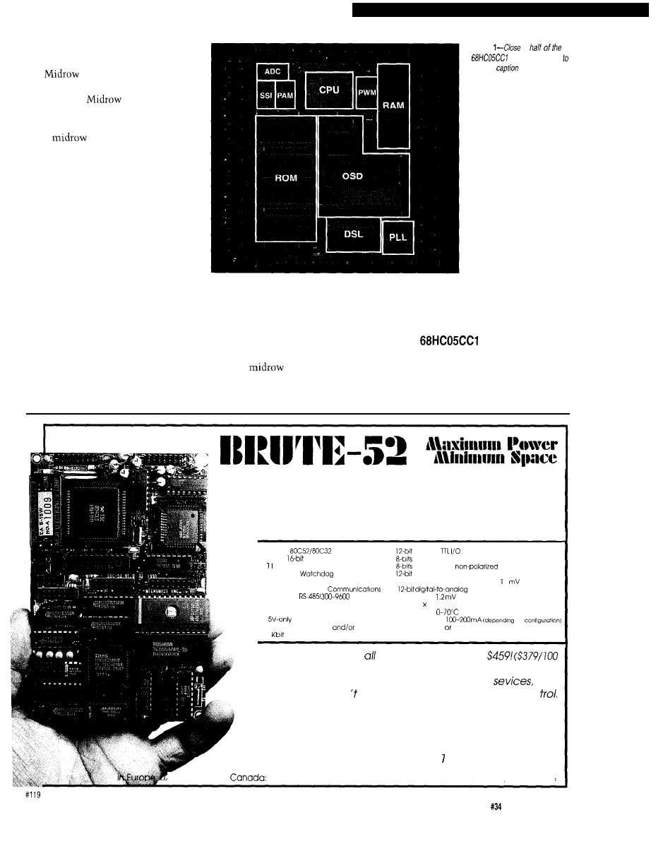
The CC1 integrated circuitry for
data extraction and special display
functions for closed captioning, are
what makes the CC1 a new generation
part. Photo shows the various
modules of the CC1 die. The
Locked Loop (I’LL). These modules
provide the data extraction and caption
display functions, respectively, for
closed captioning.
The CC 1 includes several other
peripherals on-chip to perform other
tasks not related to captioning. The
Pulse Width Modulator is used for
audio and video control. Serial com-
munication with external devices
is provided with the Synchronous
Serial Interface. The Pulse Accumula-
tor performs input pulse measure-
ments, or pulse counting, for remote
control interpretation. For communi-
cation from the TV chassis back to the
controller, there is a
ing time for the more CPU-intensive
closed-caption decoding tasks.
We’ll show you how we’ve used
the
to view captions.
We’ll set the stage by delving into the
rules for closed captioning and by
exploring the interior of the CC 1.
We’re going to describe the software
and hardware used in our setup, so
you’ll understand closed-caption
programming challenges and how the
CC1 can help you meet them.
CLOSED-CAPTION
REQUIREMENTS
The Federal Communications
Commission (FCC) was empowered by
the TV Decoder Circuitry Act to
establish rules dictating performance
and display standards for caption
decoders. The FCC worked from a
proposal developed by a task force
from the Electronic Industries Associa-
tion (EIA). The EIA, in turn, referred to
the captioning precedents set in the
1980s by the Public Broadcasting
Service (PBS] and the National
Captioning Institute (NCI). In order to
maintain compatibility with existing
decoders, the
data transmis-
sion format was left intact, but
modifications were made to the
display methods to improve captioning
and allow manufacturers additional
flexibility. On April 12, 1991, the FCC
adopted the Report and Order describ-
ing caption requirements.
To understand how captioned data
caption hardware on the CC1 consists
Digital Converter and Comparator
is transmitted, it’s best to start with
of a Data Slicer module (DSL) and an
system. The functions performed by
the “big picture” of NTSC video-the
On-Screen Display module (OSD)
these peripherals are designed not to
U.S. standard-shown in Figure 1.
which are driven by an on-chip Phase
burden the
CPU,
Video signals contain timing,
two
parity
ASCII
Horizontal Sync Pulse
63.4 microseconds
Figure 2-Caption data is found in line 21 of the vertical blanking
The run-in clock provides a timing and
reference for the
bit and is followed by bits of
data.
effective data
is bytes per second.
The Computer Applications Journal
Issue
May 1993
13
(color), and luminance (bright-
ness) information. The basic compo-
nent of a video signal is the scan line,
which begins with a horizontal sync
pulse and represents one horizontal
pass across the screen. A series of
262.5 lines constitutes a field, or one
vertical pass over the screen. Vertical
sync pulses are contained in the
invisible vertical blanking interval,
which occurs at the start of a field and
has a duration of several scan lines.
Two fields are interlaced to form a
complete picture, or frame, which
consists of 525 lines. The frame rate is
approximately 30 Hz, so the field
(vertical) rate is twice that at 60 Hz,
generating a line (horizontal) frequency
of 15.75
Caption data is embedded in line
21, which occurs during the vertical
blanking interval. Field
1
was estab-
lished by
as the location for
caption data, and field 2 has been
recommended to carry extended
services information. The format for
line 21 is shown in Figure 2. A hori-
zontal sync pulse indicates a new line,
followed by a run-in clock which
provides a timing and amplitude
reference for the start bit and 16 bits of
NRZ data to follow. Each field sup-
plies two data bytes of seven bits plus
parity. The data rate for closed
captioning on one field is 60 bytes per
second, or 480 bits per second.
Caption data is processed as
received, and each byte pair represents
a double-byte control code or two
single-byte visible characters. There
are
ASCII visible characters, and
four categories of control codes: special
characters, mid-row codes, preamble
address codes, and miscellaneous
control codes. The special characters
are visible non-ASCII characters such
as the music note; there are
16
special
characters, bringing the total printing
character set to 112. The other three
types of control codes configure the
display; before we go into detail on
them, a discussion of caption formats
is in order.
CAPTION DISPLAY
The FCC allows two display
modes-caption and text-although
text is optional and is only briefly
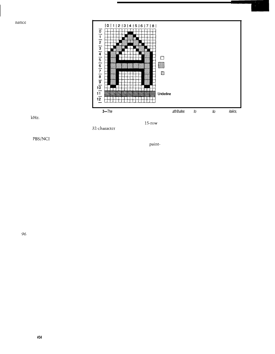
ROM-derived pixel
1
ROM-derived pixels
Rounding generated pixel
n
Black outline generated pixel
1
(hardware generated)
1
background
color
foreground
color
foreground
color
Figure
OSD ROM
character has rounding and outline
added it in addition underline,
and color information.
described. Both modes use a
by
display area. Caption
mode consists of a maximum of four
rows of characters displayed in one of
three styles: pop-on, roll-up, or
on. The features which distinguish the
three styles are how they address the
screen and how they use memory.
Pop-on style uses two 4x32 byte
memory banks: one for displayed data
and the other for undisplayed data. A
caption is stored in undisplayed
memory as it is received. When the
caption is complete, memories are
swapped, and the displayed memory
becomes undisplayed and vice versa. If
you have seen captioning, you are
probably familiar with this style.
Roll-up style uses only one
memory bank, since the caption data
is displayed as soon as it is received.
What makes roll-up style unique is the
way in which it addresses the screen.
The first row displayed establishes a
base row where each subsequent row
will appear. When a carriage return is
received, the top row disappears, the
remaining rows soft scroll upward one
row, and the new row is entered at the
base row location. Roll-up style can be
displayed with window sizes of two,
three, or four contiguous rows. This is
the most popular style for captioning
news programs.
Paint-on style is similar to roll-up
in that captions are displayed immedi-
ately, and only one memory bank is
used. Paint-on style rows do not need
to be contiguous and do not scroll.
Characters are swept across the screen
as if applied with a brush. Paint-on is
the least frequently used style.
Text mode is the optional display
mode which can show up to 15 rows of
32 characters simultaneously. It
addresses the screen like the roll-up
style of caption mode.
Captioned text in any mode or
style may take on several attributes,
such as: color, italics, underline, and
flash. Provisions are made for fore-
ground color selection from a palette
of seven colors, but compliance is
optional. Although not considered an
attribute, the background window
surrounding the caption must have
color menu choices of black and
transparent. Italics are required, but
may be implemented as a special
character set, or by slanting the
standard character set. The underline
attribute adds a line under printing
characters, and the flash attribute
causes text to blink on and off.
Attributes are assigned by preamble
address codes, mid-row codes, and
miscellaneous control codes.
CONTROL CODES
Preamble address codes are used at
the beginning of a row to identify the
row number (location on the screen),
an optional indentation, and the
default attributes (color, italics, and
underline) for the row. Preamble
address codes are nonspacing charac-
ters, though they may alter the char-
acter cursor to indent. Indentation is
14
Issue
May 1993
The Computer Applications Journal
nondestructive, so a row that already
has characters in it may be modified.
codes are used, as the
name implies, in the middle of a row
of characters.
codes affect
color, underline, and italics. They can
also disable the flash attribute. Note
that a
code appears as a
background space, limiting the use of
attributes to emphasize entire words
or phrases.
Miscellaneous control codes
perform all of the odd jobs of
captioning. The most complicated
miscellaneous codes are those that
initiate, continue, or change display
modes or styles. They are sent fre-
quently, even when the style isn’t
changing, to ensure that switching
receiver channels does not disrupt
captioning. There are also miscella-
neous codes which affect the memory
banks, by either erasing displayed or
undisplayed memory, or swapping
memories. The Carriage Return code
causes the display to soft scroll upward
in caption mode’s roll-up style or in
text mode. Other miscellaneous
commands can modify the character
cursor or row contents by backspacing,
tabbing, or deleting to the end of the
row. Flash is the only attribute set by a
miscellaneous code; it affects all
subsequent characters in a row until
the next
code.
Now you should have a good feel
for how captions must be decoded and
Photo
to
die is dedicated
closed
decoding and
control. The rest contains the
normal
CPU, ROM, RAM, and
support sections.
displayed. It would be
impossible for us to
relate all of the
requirements and
recommendations
made by the groups
involved in defining
closed captioning.
There are several
documents which
you can obtain for
more information. A list of these
references is included at the end of this
article.
THE
CAPTION
SUBSYSTEM
The DSL and OSD perform the
decoding and display tasks of the
caption subsystem, but they could not
Micromint’s BRUTE-52 is the ultimate compact controller.
One look at the list of features will tell you that this full-
featured controller has the power to crush your most de-
manding applications:
. CMOS
.
parallel
l
Three
counter timers
.
buffered high-voltage. high-current outputs
.
0592 MHz System Clock
.
optoisoloted
DC inputs
l
Hardware
Timer
.
plus sign analog-to-digital converter
. Hardware Clock-calendar
8 channels! 60 Samples/second! 2
resolution!
. Optoisolated Serial
l
converter
RS-232 or
bps’
2 channels!
resolution! Selectable ranges!
. Optoisolated Serial Printer Port,
. Only 3.5 5 3 Inches!
RS-232 150-9600 bps
. operates at
l
Operation
l
Consumes only
on
l
Up to 56 Kbytes RAM
EPROM
l
Use networked stand-alone
. 1
EEPROM
l
DEMO/Diagnostic ROM
BRUTE-52
offers you these features at only
quantity
OEM)
We also have a starter system for $289. When
you add in Micromint’s renowned quality,
and
support, you won find a better value in compact con
To order BRUTE-52, or for more information, contact:
Micromint, Inc.
4 Park Street
l
Vernon, CT 06066
Phone (203) 87 l-6 70
l
FAX (203) 872-2204
(514) 336-9426
l
in Australia: (02) 888-6401
l
Distributor lnauiries Invited!
785658122
l
in
The Computer Applications Journal
Issue
May 1993
15
function without the PLL. The OSD
and DSL both need to be synchronized
with the TV chassis, and the OSD
requires a fast clock for dot processing.
The PLL provides several stable
frequencies which are phase locked to
the horizontal sync from the chassis.
The fastest of these is a
clock which provides the internal
horizontal timing for the character
pixel display. There are two pins on
the CC1 that are dedicated to tailoring
the loop filter and center frequency.
DATA SLICER
The Data Slicer consists of
circuitry for sync and data recognition,
line detection, and data acquisition.
Sync and data information from the
composite video pin is separated by
the slicer circuitry. The separated sync
contains both vertical and horizontal
sync pulses. The difference in time
between the rising edge of the horizon-
tal sync and the rising edge of the
vertical sync distinguishes between
fields; data can be extracted from both
fields.
A line detector counts horizontal
lines from the vertical sync interval to
find line 2
1,
which contains the
closed-caption information. This
triggers the data acquisition block to
begin sampling data. Sampled data is
converted from serial to parallel
format and stored in registers along
with the results of the parity checking.
ON-SCREEN DISPLAY
The On-Screen Display consists of
a register array, character ROM,
synchronization, and output blocks.
Patterns for characters that are
referenced in the register array are
fetched from
OSD character ROM
and processed by the output block
under control of the synchronization
logic.
The register array contains 9 bytes
for display control, position, status and
test. In addition, there are 34 character
registers which hold the OSD ROM
page addresses of the characters to be
displayed on a single row. The charac-
ter registers and some of the control
registers are double buffered, which
allows for dual
access. The
OSD can be enabled after the character
Listing
code attributes are deciphered from the second byte, combined into an
video
control code, and inserted into the RAM caption
* MRPROC: Mid Row control code
*
Interprets a Mid Row control code.
* Inputs: none
* Outputs: none
* Flags: none
MRPROC LDA
BEQ
MRDONE
CMP
SELMODE
BNE
MRDONE
LDA
STA
PREVCH
GETATTR
JSR
VISCHAR
STA
MRDONE RTS
see if
code is for selected mode
ignore
code if mode not set yet
ignore codes not for selected mode
update previous character indicator
get color, italics, underline attr
put character in memory
retrieve MKC that was put in memory
update current video control value
* GETATTR: GET
from control code
Parses control code for color, italics, and underline
information.
* Inputs:
none
* Outputs: attributes in video control format in A
Flags:
none
GETATTR LDA
get attr (2nd) byte of control code
LSRA
shift to get rbg as bits
AND
mask off all other bits
BEQ
WHITE
000 = white
CMP
#COLORS
BNE
GETUL
ITALICS LDX
PREVCH
check to see if this is PAC or MRC
if
italics makes color white
LDA
if MRC, italics uses previous color
AND
get current video
color value
set italics bit
BRA
GETUL
WHITE
set
= for white
GETUL
BRCLR
set underline bit if indicated
add two
to indicate video
RTS
and default control codes for the first
row to be displayed are loaded into the
registers.
The OSD character ROM contains
128 9x13 bit matrices that can store a
custom character set. Individual bits in
each character matrix block represent
a square of four video pixels of either
foreground or background video. The
contents of the OSD ROM are speci-
fied at the time of product order along
with the contents of the program
ROM.
The synchronization block in the
OSD controls the timing of the display
of closed-caption data. It uses the
and
external inputs from
the chassis and the PLL output
frequencies as references. The sync
block maintains timing for dots,
characters, lines, and fields. The event
line number, stored in an OSD
register, indicates the position of the
first scan line of a character row to be
displayed. When a match occurs
between the scan line number and the
event line, the display process begins.
Character codes are sequentially
read from the character registers
during each scan line. Each code, along
with the scan line number within the
character row, is used as an address to
1 6
Issue
May 1993
The Computer
Journal
fetch the appropriate
“slice” of
horizontal data from the character
ROM. Vertically adjacent line patterns
are also fetched to provide data that
the output logic uses to interpolate the
character cells for rounding and black
outline of characters. A sample OSD
ROM character with added rounding
and outline attributes is shown in
Figure 3. The output logic also adds
underline, italics, and color informa-
tion. The bit patterns drive the red,
green, and blue color outputs and fast
luminance blanking output which
communicate with the color guns of
the TV.
At the time of an event match, the
user is signaled with an interrupt that
indicates the OSD is ready for the next
row of character codes to be loaded
into the OSD registers. The shortest
time available to the program for
updating the registers with the next
row codes extends from the beginning
of the currently displayed character
row (at the time of the interrupt) to the
end of that row. This is the case if the
next row to be displayed is directly
below the currently displayed row. A
rate of 262.5 scan lines (one field) in
of a second gives 63.49 microsec-
onds per line. Each character row has
lines, so that leaves a minimum
interval of 825 microseconds to load
the next row codes. The
internal bus frequency of the CC1 is
double that of its predecessors in order
to facilitate servicing of the OSD.
OSD CLOSED-CAPTION
FEATURES
The architecture of the OSD
provides the flexibility required to
perform closed captioning, but the
display aesthetics are determined by
the received data. Video control codes,
which appear on the screen as a
background color space, can be
inserted anywhere in the character
row. Video control codes are used to
implement the closed-caption mid-row
codes, which can change the current
character foreground color, italics, and
underline selections. The
caption miscellaneous control code for
character flash uses the video control
codes as well. The ability to change
the appearance of text within a row is
Listing
copies the RAM display buffer and the video control code, matrix register, and event
line the
regisfer block.
*
CPDATA:
DATA from display buffer
* Copy the video control character and character
data from the display memory row into the OSD.
*
Inputs:
Index to row to be copied in X
* Outputs: none
Flags: none
CPDATA LDA
STA
OSDVCl
ADD
STA
OSDELN
LDA
copy video control byte
STA
LDA
CCHD
copy horizontal delay
STA
OSDHD
LDA
CCMR
copy matrix range
STA
OSDMR
LDA
CCBOR
copy border
STA
OSDBOR
LDA
determine index into display buffer
MUL
TAX
STX
TBUFPTR
offset from start of buffer to char
LDX
INCX
CPLOOP STX
TOSDPTR
update pointer to OSD registers
LDX
TBUFPTR
get pointer to buffer
LDA
get character from buffer
INCX
STX
TBUFPTR
update buffer pointer
LDX
TOSDPTR
get pointer to OSD
STA
copy character to OSD
INCX
copy 32 bytes
BNE
CPLOOP
CLR
clear first and last characters in row
CLR
OSDCH34
LDA
first last solid spaces selected?
CPDONE
don't add solid spaces if not selected
BRCLR
LDX
search for first solid space
SPFIRST
INCX
look for visible
in row
only search through 32 characters
BEQ
CPDONE
LDA ,X
BEQ
SPFIRST
if a nonborder space character
DECX
LDA
then put a space in previous location
BRCLR
LDA
if
sets underline, delay
B C L R
underline set to 1st space
STA
store 1st "space" (space or new
LDX
search backward to last solid space
SPLAST DECX
look for visible
in row
only search through 32 characters
CPDONE
LDA
SPLAST
if a nonborder space character
INCX
LDA
then out a default
STA ,X
(to remove underline) in last space
CPDONE
copy video control byte
copy event line
add Roll Up offset
RTS
18
Issue
May 1993
The Computer Applications Journal
very important to a hearing-impaired
individual watching a captioned
broadcast, since it adds another
dimension of expression to an other-
wise lifeless line of text.
The roll-up closed-caption style
requires that the display scroll verti-
cally in a window. The OSD includes a
special control register which, when
modified in conjunction with the
event line register, results in soft
scrolling. The upper and lower nybbles
of the matrix range register are used to
select the scan lines where character
foreground should begin and end,
respectively. A character row consists
of 13 scan lines; any lines outside the
character matrix range appear as
background. Scrolling a roll-up caption
involves shifting the existing rows up
by decreasing their event lines, and
appending the new row by decreasing
its event line while increasing its
matrix range. Of course, the changing
of the event line and matrix register
must occur at an appropriate fre-
quency. The FCC recommends a rate
of one line per frame.
A CLOSED-CAPTION
APPLICATION
Our goal was to program the
to decode and display
closed captions in a television. We did
not incorporate the code required to
control general TV functions and
interact with the user. This simplified
the programming task, but we wrote
the software to accommodate addi-
tional burdens on the CPU, RAM, and
ROM.
The critical issues in software
development were time and memory.
The time constraints were set by the
service requirements of the OSD.
Memory was given special consider-
ation because of the large amount of
RAM required to store the captions.
The 16K ROM was more than suffi-
cient for the 2K of decoding software.
The OSD can be very demanding.
The minimum interrupt interval of
825 microseconds makes OSD
underflow, and subsequent display
distortion, a distinct possibility. We
prevented underflow by minimizing
the OSD service routine and by using
SE
I
instructions sparingly throughout
the rest of the code. The only code
segments protected from interruption
are those that modify the buffer
containing the screen addresses of the
caption rows.
The concern with RAM require-
ments was that text mode requires
nearly 512 bytes, and the
not
intended for full text mode, has only
bytes. We made a compromise
that limited the text mode window to
eight rows, and shared the text
memory bank with the memory used
for caption mode.
SOFTWARE FUNCTIONALITY
The software has two main tasks:
interaction with the CC1 display
subsystem, and closed-caption data
interpretation. The interaction with
the DSL and the data interpretation
occur serially, in parallel with the
interaction with the OSD.
The data slicer itself doesn’t
require much assistance. After initial-
izing the control registers, all that
needs to be done is a read of the data
registers and status register upon an
interrupt.
Once the two bytes of caption
information have been retrieved from
the data slicer, the interpretation
phase begins. The first step is to
determine whether the two bytes form
a control code or two visible charac-
ters; a data parity check is also made
for either case. Correct visible charac-
ters are copied directly into the RAM
caption buffer, since there is a
one mapping from ASCII code to OSD
character address. Control codes may
also end up as characters in the
caption buffer, or they may modify the
buffer, its pointers, or the actual
display.
Control code processing includes
checks for duplication and data stream
selection. The leading byte of a control
code addresses one of two data streams
chosen by the viewer. All subsequent
data, until the next control code, is
directed to the data stream indicated
in the first byte, and the software must
discard the unused control codes and
visible characters.
Both bytes of a control code are
used to determine its type, and each
type is processed separately. Once a
R E L A Y
INTERFACE
INTERFACE . . . . . . . . . . . . . . . . . . . . . . . $89.95
Two channel relay output
are
of
up to relays (expandable to 128
expansion cards).
relay
to
relay card or terminal
A variety of relay
relays stocked. Call for more info. RS-422 available
(distances to
feet). PS-4
selector may be
to
AR-16
(up to 16,384
REED RELAY CARD (6
10 VA) . . . . . . .
49.95
RELAY CARD
amp SPDT
69.95
RELAY
EXPA
CARD (16
D I G I T A L
ADC-16
A/D CONVERTER (16 channel, 6
temperature,
usage. energy
levels, joystick movement end
amperage,
of other
of analog
may
be
AD-1
nded to 32 analog or 128 status
using the
or ST-32 expansion cards. 112 relays may
controlled using
expansion cards. Anal
in
may be configured for temperature input using
E-6
temperature input
RS-422 available. PS-4 port
may be used to connect satellite ADC-16
(up 4,096 analog
status inputs
14,336 relays). Call for info on 10 12 converters.
block and cable sold separately)
ST-32 STATUS
CARD . . . . . . . . . . . . . . . . . . . . . . $79.95
“put on/off status of relays, switches. HVAC equipment,
security
smoke detectors end other
including keypads and binary coded outputs.
32 status
isolators
separately).
TEMPERATURE INPUT CONVERSION . . . . . . . . . $49.95
6
sensors
block.
ran
‘S-4 PORT SEL
e is minus 40 to 145 degrees F.
CTOR
RS-232
(4 channels
. . . . . $79.95
4
RS-422 ports.
TONE
serial interfacing
available. Call for free
packet.
FULL TECHNICAL
over the
telephone by
staff. EACH ORDER INCLUDES A
FREE DISK WITH PROGRAMMING EXAMPLES IN
BASIC, C AND ASSEMBLY LANGUAGE. A detailed
reference manual is also included.
HIGH RELIABILITY.. engineered for continuous 24
hour industrial applications. All
socketed.
Use with
and compatibles, Tandy, A
Mac and
most other computers with AS-232 or
ports.
All standard baud rates and protocols may be used
(50 to 19,200 baud).
Use our 600 number to order FREE INFORMATION
PACKET. Technical Information (614)
2 4
H O U R
O
R D E R L I N E
Express-COD
International Domestic FAX (614)
Use for
technical support orders
ELECTRONIC ENERGY CONTROL, INC.
South Fifth Street, Suite 604
Columbus.
43215
The Computer
20PF
Figure
a
of external components,
accepts video, horizontal sync, and vertical sync, and
drives the red, green, and blue CRT
guns in the television, superimposing closed captions
when
special character has been identified,
the second byte, combined into an
its second byte is translated into the
OSD video control code, and inserted
appropriate OSD character code and
into the RAM caption buffer. A
treated as a visible character.
preamble address code incorporates
code attributes are deciphered from
row selection in its first byte, and
attribute and indentation information
in its second byte. This code causes
the processor to select a new row in
the RAM buffer, modify the character
cursor, and set up the default video
User Console Program, DOS.
Shown: Edit Window at left
Teach Window at right,
Status Window at bottom.
Manipulator Breadboard.
Shown: 2 fingers,
each with 2 motors.
The
RCS-6 is a
table-top,
Robotic Construction System (RCS) which can be
used to build and operate robotic models. The
combination of ease of construction, advanced
user interface, and low cost deliver previously
unavailable levels of value and performance to
the robotic enthusiast. The control algorithms, user
interface, and both low and high-level program-
ming interfaces are superior to any others in this
price range.
Use Robix Ian uage with built-in editor and
teach-pendant mo e for sequencing. Extend
with calls from C or QB 4.5.
Connect to DOS PC’s
by
A / D , 7 switch inputs, 2 outputs. Software pro-
vides auto-matched velocity trapezoids, per-axis,
maxspd,
pos,
moves, and more.
Robix
complete (less printer cable):
Advanced Design, Inc.
1101 E. Rudasill Road, Tucson, AZ 85718
voice: (602) 544-2390 fax: (602) 5750703
5
Axis + Parallel Jaw Gripper.
‘Assembly time of approx 15 min
is typical for most constructs.
Table-Tennis Golfer.
3 coordinated “swing” axes,
4th axis controls club “loft”.
22
Issue
May 1993
The Computer Applications Journal
Roll-Up Captions-4
Mid-Row: Yellow Underline
Carriage Return
This is [I 1
VERSION THREE
[I 4
of a proposed test tape
14
for the line-21
closed-captioning system.
PAC: Row 15, Indent 4
me rest rape
several
of Me closed
system. The final output generated by this
stream is in Photo 2.
control codes for the new row. Miscel-
laneous codes can be distinguished by
their second bytes. They alter the
RAM buffer or character cursor and
must be processed on an individual
basis.
The code segment featured in
Listing 1 is responsible for interpreting
codes.
M R P ROC
checks for the
selected display mode before calling
G
ETATT R
to extract the attributes.
GETATTR
converts the color, italics
and underline selections into a video
control code, which is passed to
PUTVC
(not shown) for storage in the RAM
display buffer.
The OSD interrupts the data
interpretation process up to four
(caption mode) or eight (text mode]
times per field to obtain a new row of
characters to display. Once the
software has determined that there is a
next row to display and which RAM
buffer row that it corresponds to, the
routine in Listing 2 will be accessed.
C
P DATA
copies the RAM display buffer
and the video control code, matrix
register, and event line to the OSD
register block. Optional first and last
space characters are added to the row
in accordance with FCC guidelines.
We balanced the needs for quick
response time to the OSD and compact
code writing this subroutine.
We used three tools to aid in code
development. The MMDS05 develop-
ment system is a compact emulator
and bus state analyzer which commu-
nicates with both the target system
and an IBM-compatible host computer.
It consists of a generic
ible platform that supports microcon-
troller-specific personality boards-in
this case the
EVS.
Although it lacks the bus analysis
capability, the EVS was also useful as a
stand-alone debugging tool. The
smallest tool used in code
This special version of the
pin SDIP package holds a CC1 inter-
nally, and accommodates the plug-in
of a standard 28-pin DIP EPROM that
acts as the user ROM. Use of these
tools significantly decreased develop-
ment time.
Putting the project together was
ment was the
a
not too difficult, with the exception of
back” emulator of the
watching holes being drilled in the
Mat is
ROM
Your
Borland
or
Microsoft
is the
ROM development software tool
lets you run Microsoft and Borland C and C++ programs on an
embedded
CPU without using DOS or BIOS.
saves you money. There are no DOS or BIOS royalties
to Pay for
your embedded systems.
complete! It includes the following and much more:
*Supports Borland’s Turbo Debugger.
*Remote Code View style source level debugger.
startup code brings CPU up from cold boot.
l ROWlable library in source code.
*Flexible 80x88 Locator.
PACKAGE
GACK
The Computer Applications Journal
Issue
May 1993
2 3
cabinet of our brand new 27” color TV.
Safety and space constraints forced us
to mount the CC1 on a small bread-
board which we attached to the
television cabinet. The schematic of
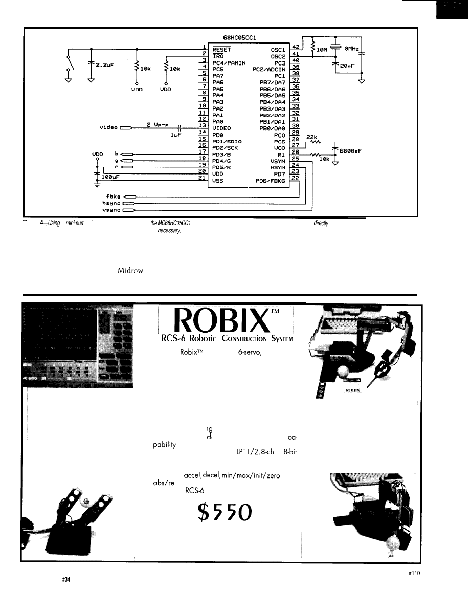
the CC 1 breadboard is included in
Figure 4.
There were seven signals routed in
short coaxial cables between the
chassis and the
composite video;
chassis
and
and red,
green, blue, and fast blanking. The
composite video was taken from the
chassis video processor chip, and the
other signals were connected to the
existing OSD microcontroller socket.
The original microcontroller was left
in place to perform the general TV
control functions, but the color and
fast blanking signals were discon-
nected to prevent contention with the
This meant that our modified
television would no longer have
regular (noncaptioned) on-screen
display. In systems where the CC1 is
given full control of the TV, this
would not be the case.
As you can see in Photo 2, the
CC1 performed with flying colors.
This photo shows a caption display
generated by the CC 1 from data it
extracted from a test tape. The closed
captioning transmitted with most
shows and movies marginally exer-
cises FCC requirements, so we relied
on a set of videotapes designed to test
decoders exhaustively. The source for
these tapes is listed at the end of this
article. Figure contains an example
of the data stream on the test tape that
was used to generate the caption seen
in Photo 2.
CONCLUSION
The Television Decoder Circuitry
Act has opened new channels for
transferring information to the
viewing public. The medium for which
this act was initially intended is closed
captioning. Already, though, there is
discussion by the TV Data Systems
Subcommittee of the EIA for extended
data services, which would allow for
other types of information to be
relayed to viewing audiences via
printed text on a television screen.
Examples include information about a
current program such as length of
feature, program title, and rating, or
emergency messages from the Na-
tional Weather Service.
We’ve given you some insights
into what’s required to build a
caption decoder, and we showed an
example of a working system that uses
the
to implement closed
captioning. Television broadcasters
will be offering more and more
captioned programs in the near future,
and will eventually incorporate
extended data services. The CC 1,
which relies on software to perform
Photo
installed in a new
set, the
sample
circuit
performs with flying
colors
24
Issue May 1993
The Computer Applications Journal
data interpretation, has the flexibility
to support both closed captioning and
extended data services.
q
Janice Benzel holds BSEE and MSEE
degrees from Purdue University. Linda
Reuter
holds a BSEE degree
from Texas Tech University and an
MSEE from the University of Texas.
They both design customer-specific
microcontrollers at Motorola in
Austin, Texas.
Motorola Semiconductor Products
2100 East Elliot
Tempe, AZ 85284
(602) 244-6900
TWX: 910-951-1334
Television Decoder Circuitry Act
of 1990, Pub. L. 101-431.
“Television Captioning for the
Deaf: Signal and Display Specifi-
cations,” Engineering Report No.
E-7709-C, Public Broadcasting
Service, 1980.
“Telecaption II Decoder Module
Performance Specification,”
National Captioning Institute,
Inc. 1985.
Report and Order, Federal
Communications Commission
GEN Docket No. 91-1, 1991.
Memorandum, Opinion, and
Order, Federal Communications
Commission GEN Docket No.
91-1, 1992.
“Line 21 Data Services for
NTSC,” Electronic Industries
Association EIA-608, 1992.
Caption Test Tapes:
The Caption Center/MARDO
WGBH Educational Foundation
125 Western Ave.
Boston, MA 02134
401
Very Useful
402 Moderately Useful
403 Not Useful
Vector
Approach
Simplifies
Dimensional
Graphics
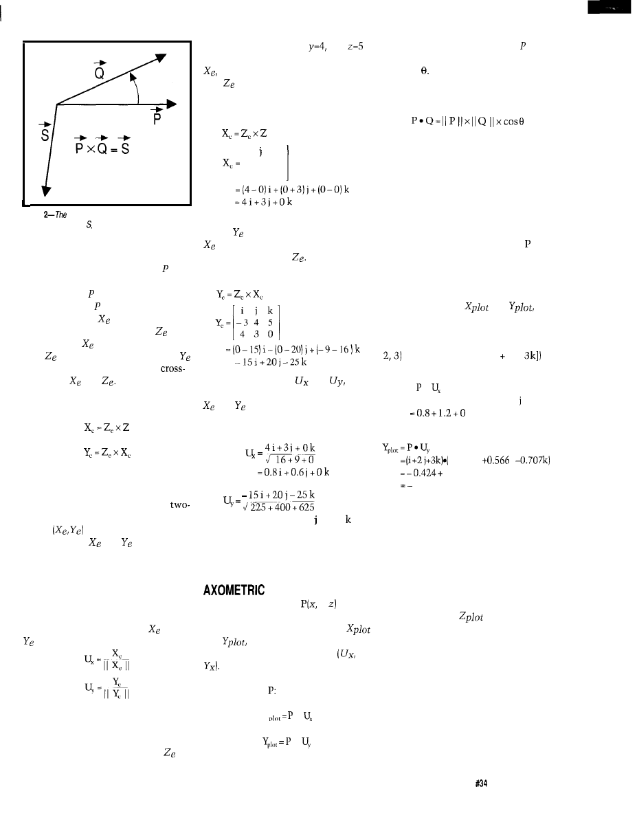
Fred H.
tion of three-dimensional drawings on
a two-dimensional display device. The
calculations can be greatly simplified,
and the use of trigonometric functions
almost eliminated, when mapping
There are three basic steps you
must take when creating a
points from an abstract, three-dimen-
dimensional view on a two-dimen-
sional display device. First, you need
to establish a viewing plane (or screen)
sional object space onto a
perpendicular to the viewer’s direction
of sight. Second, you need to project
dimensional plotting surface.
the points and lines from any objects
in a three-dimensional object space
onto the plane of the display screen.
Third, you need to
adjust the lengths of
any projected lines or
surfaces in the display
plane to provide the
illusion of perspective,
or depth cues, where
they are desired.
In addition, we will assume the
Assuming the viewer’s center of
viewer wishes to see the object in the
vision is directed at the origin rein-
forces the idea that the viewer’s path
upright position. That is, the Z
of vision is directly along the
axis.
Also, the origins of the viewing
coordinate points toward the top of the
coordinate system and the object
coordinate system are coincident,
object. [If another direction for “up” is
since they intersect at the point (O,O,O).
Objects not centered about (O,O,O) may
be easily moved by linear translation.
required, then you need to specify a
vector pointing in the desired direction
instead of Z.)
The Z axis of the object coordinate
system lies in the plane formed by
and
It is necessary to locate the
coordinates of this point in the
plane, and a mathematical property
that can be used for this is the vector
cross-product. The vector
product takes two vectors as inputs to
the calculation, and yields a third
vector that is perpendicular to both the
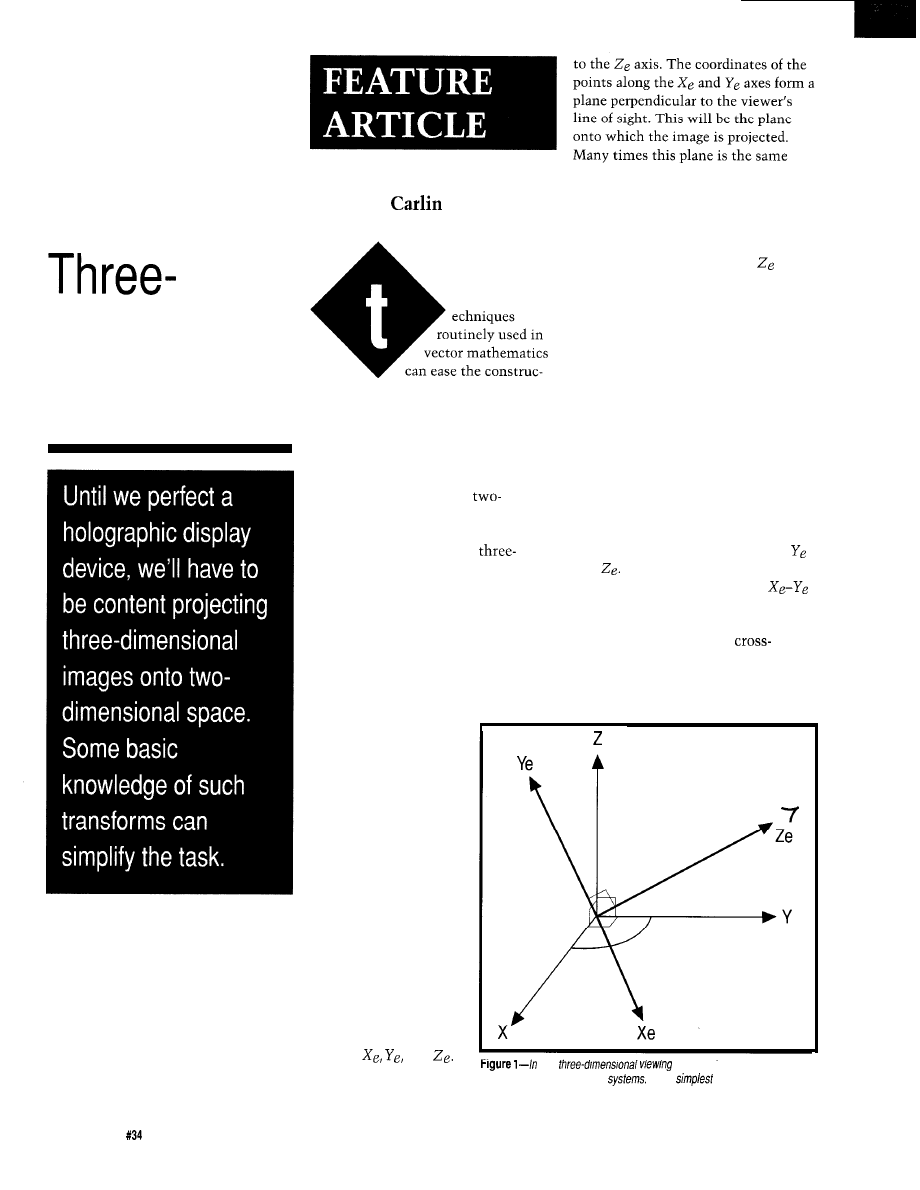
Figure
1 shows two
independent coordinate
systems that intersect
one another at the
origin. The first system
is the object coordinate
system whose axes are
marked X, Y, and Z.
The other is the
viewer’s coordinate
system whose axes are
marked
and
Note that the viewer’s
line of sight is parallel
any
system, there are separate
object and viewer coordinate
In the
case, they both have a
common origin.
plane as, or is parallel to, the screen’s
display surface.
26
Issue
May 1993
The Computer Applications Journal
Figure
vector cross-product of P and Q
generates the vector which is perpendicular to the
first two.
first and second vector. Figure 2 shows
that the cross-product of vectors and
Q yields the vector S that is perpen-
dicular to both and Q (and hence the
plane formed by and Q). We can
obtain the vector
by taking the
vector cross-product of vectors and
Z. The vector
is perpendicular to
both and Z. Similarly, the vector
is obtained by taking the vector
product of and
These state-
ments can be summarized with the
following mathematical expressions:
The information required to
project a point from the three-dimen-
sional object space (X, Y, Z) to the
dimensional plane of the display
screen
is obtained by convert-
ing the vectors
and to unit
vectors. A unit vector is a vector that
is precisely one unit in length in a
given direction. Unit vectors are
obtained by dividing each coordinate
of the vector by the magnitude of the
vector. The equations used to calculate
the unit vectors from vectors
and
are:
I will illustrate the application of
these formulae in the following
example. Suppose the viewing position
of an object lies along the vector
and is at the point x=-3,
and
in the object coordinate system. Then
a vector perpendicular to both Z
and (which is a vector from the
viewing position to the origin) is found
as follows:
i
k
-3 4 5
i
0 0 1
The next step is to compute the
vector using the just derived vector
by using it in the cross-product
formula with vector
These calcula-
tions are shown below:
=
The unit vectors
and
which are derived from the vectors
and respectively, are calculated
as follows by applying the unit vector
formula to each vector independently:
= 0.424 i + 0.566 0.707
With these points calculated we
are ready to go on to the calculation of
the points to be plotted on the screen.
DISPLAY
Projecting a point
y, onto
the viewing screen requires calculating
the plot screen coordinate values
and
which are the projected
equivalent values for the point
These are calculated by using the
dot product of each of the unit vectors
with the point
X
l
l
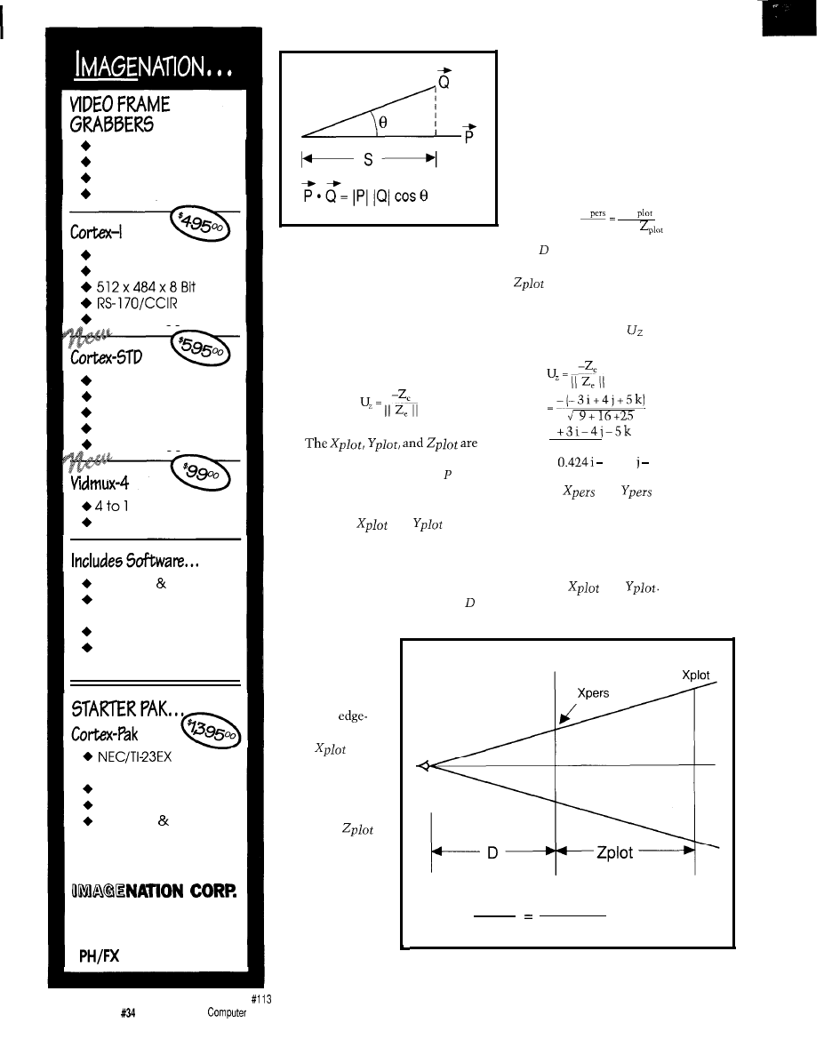
Figure 3 shows two vectors and
Q with their included angle, desig-
nated as The dot product formula
shown above for these vectors is also
equivalent to the following formula:
If Q is a unit vector (defined as
having a length of exactly 1 unit] and
lies on the principal axis of the object
coordinate system, Z, then application
of the dot product will yield the
distance that the point is along the Z
axis, or away from the X-Y plane. This
distance is labeled as “S” in Figure 3.
The value of S will be positive if is
on the same side of the X-Y plane as Q
and negative otherwise.
I will illustrate the use of the dot
product to calculate the screen
coordinate values,
and
by
continuing with the same point
coordinates as I used in the previous
example, the plot values for a point
(1,
(or vector end point [i 2j +
is:
Xplot =
l
= (i + 2 j + 3 k)
l
(0.8 i + 0.6
+ 0
k)
= 2.0
-0.424 i
j
1.132-2.121
1.413
As a result, the point at (1, 2, 3)
would project onto the screen at the
X-Y coordinate point (2.0, -1.413). All
you have to do now is to scale or
adjust the plot value for the screen or
plotter coordinates.
Recall, the unit vector calcula-
tions need be performed only once for
any viewing position in three-dimen-
sional space. The
is ignored in
the axometric display, which results in
collapsing the Z dimension.
PERSPECTIVE DISPLAY
A perspective display is generated
in a similar manner to the axometric
display. In the perspective display
system, the distance from the observer
is taken into account and the object
scaled appropriately. This is easily
accomplished with some additional
The Computer Applications Journal
Issue
May 1993
27
Simplicity
Functionality
Affordability
Accuracy
Real-Time Capture
Half Slot XT/AT
External Trigger
Dual Video Input
Opt. XMS Mapped
Low Power Options
STD-80 or 32 Bus
External Trigger
MUX
Half Slot XT/AT
C Library Source
Image Capture
Utility
Tiff Utilities
“Image” Drive
Ram Disk Emulation
Camera
With Lens
9” Video Monitor
Frame Grabber
Software Cables
OEM PRICING AVAILABLE
P.O. Box
84568
Vancouver, WA 98684
(206) 944-9 13 1
Figure 3-The vector dot product or scalar product
projects the shadow of one vector on to the other.
information regarding how far the
point is from the viewing screen. This
is done by first finding the unit vector
perpendicular to the Xe-Ye plane or
screen. This vector has been previ-
ously established and its unit value is
simply:
formed by the dot product of the
vector described by the point and the
unit vectors of the viewing coordinate
system. Perspective is added by
adjusting the
and
values
by the distance that particular point is
from the observer.
The reasoning behind this is
shown in Figure 4. It shows a diagram
of an observer located a distance in
calculations for any of the Y values are
also omitted from the discussion. The
arguments and computational meth-
ods for the Y values are identical to
those for the X values except the
variable values for any Y value are
substituted for each X value.
Perspective scaling is obtained by
using the following relation:
X
X
D
D +
is the distance the observer is
from the origin of the viewing plane.
is the distance from the viewing
plane to the point to be displayed. I
can, referring to our example, calculate
the unit Z vector or
by using the
following:
7.07
=
0.566
0.707 k
The
and
values (i.e.,
the ones used to plot points on the
screen) are found by first calculating
the distance the viewer is from the
screen. This distance is used in the
relations that are used to adjust the
values of
and
These
operations are shown below:
front of the
viewing plane.
The viewing
plane passes
screen
through the origin
and is shown in
the figure
on. A typical
point
is
shown trans-
formed and
plotted in three
dimensional
space (i.e.,
units behind the
viewing screen).
Note that to
keep Figure 4
simple, the Y axis
values are not
Xpers Xplot
D
shown in the
D + Zplot
figure. This being
Figure 4-Scaling for perspective is proportional to distance from the viewing screen
the case, all
or plane.
28
Issue
May 1993
The
Applications Journal
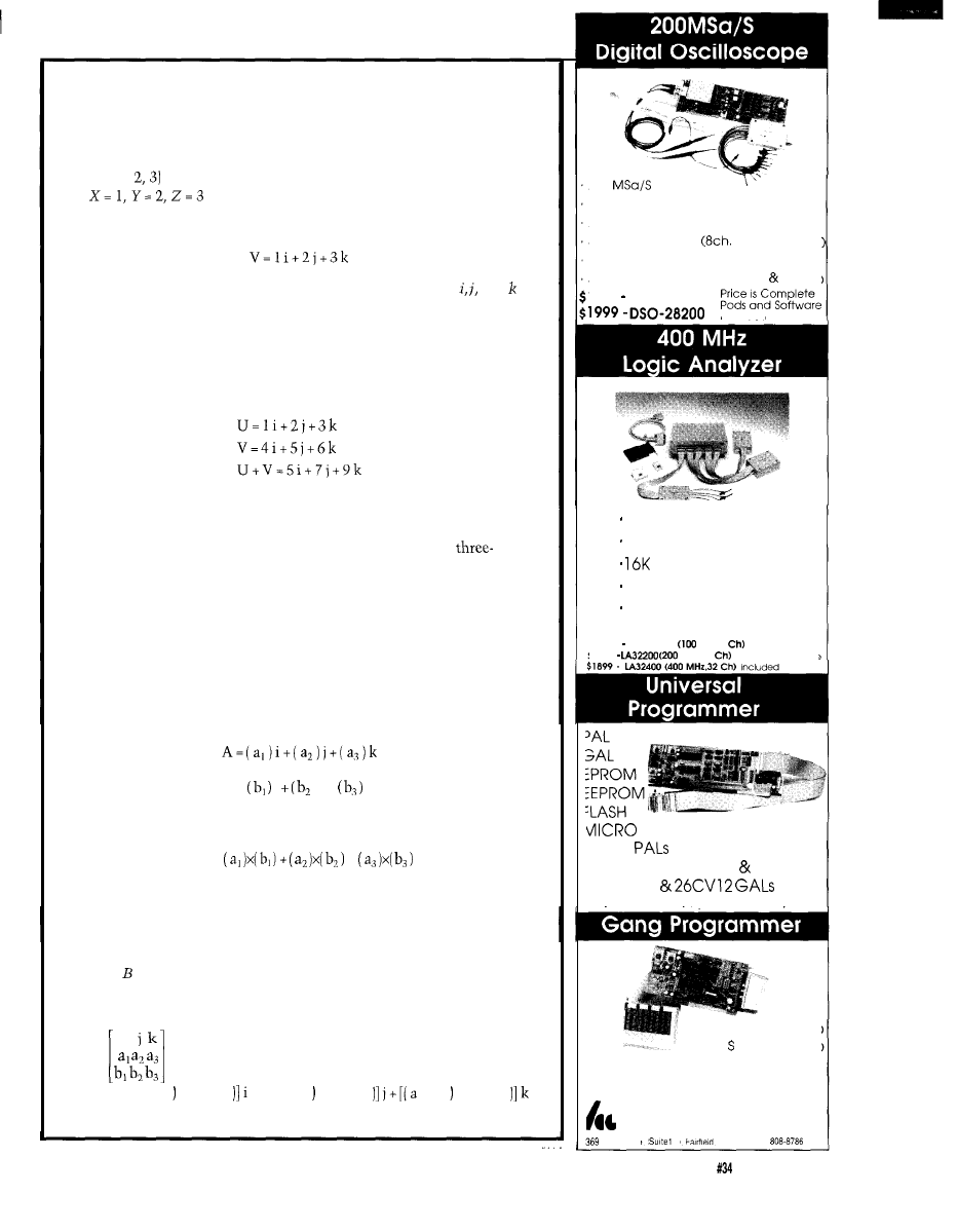
VECTOR MATHEMATICS
A three-dimensional vector can be represented as an array of three
numbers, each corresponding to one axis of the three-dimensional
coordinate system. For example:
V =
(1,
is the notation for a vector from the origin to the point
This vector can also be written in its equation form as:
When vectors are represented in this form, then the variables and
are tags to label the values corresponding to the respective values for X, Y,
and, Z.
ADDITION
The addition of two vectors is accomplished by adding their corre-
sponding parts. For example:
MULTIPLICATION
There are two types of vector multiplication: The dot product and the
cross product. Each has special properties that can be used in
dimensional plotting.
DOT PRODUCT
The result of a dot product is a simple numeric value or scalar. The dot
product is numerically equal to the length of vector A times the length of
vector B times the cosine of the included angle.
Graphically, the dot product projects the first vector onto the second
and the numeric value is the length of the projection or “shadow.” For
example:
B =
i
) j +
k
Then the dot product is easily computed from:
A
l
B =
+
CROSS PRODUCT
The result of a cross-product is a new vector. This vector has special
properties that make it very useful in three-dimensional graphing applica-
tions: First, its length is equal to the length of vector A times the length
of vector times the sine of the included angle. Secondly, the new vector
has a direction perpendicular to both vectors A and B. An example of a
cross-product calculation is shown below:
i
A x B =
=[(a xb (b xa [(a xb (b xa
xb (b xa
200
sampling rate
PC-BASED INSTRUMENT
2 Analog channels
8 Digital channels
logic analyzer
125MHz Single shot Bandwidth
4K samples/channel (analog digital:
1599 DSO-28 100
included
up to 128 channels
up to 400 MHz
samples/channel
Variable threshold
8 External clocks
16 level triggering
$799 IA12100
MHz,24
Price is Complete
$ 1 2 9 9
MHz,32
Pods and Software
5ns
$ 4 7 5
4 MEG EPROM (8 16 bit)
22V 10
Free software updates on BBS
$ 215 (4 Socket:
299 (8 Socket:
Up to 1 MEG EPROMS
Call (201) 808-8990
Link Computer Graphics, Inc.
Passaic Ave.
100.
NJ 07004 fax.
8 1 1 4
The Computer Applications Journal
Issue
May
1993
29
= 7.07
Zplot =
l
= 2.829
=
2.829
1.413 x 7.07
2.829
= 2.356
Note that the
and
values are larger than the corres-
ponding
and
values
because the point is closer to the
viewer than the viewing screen formed
by and
CONCLUSIONS
The vector and point manipula-
tion equations that I used in this
discussion often form part of the core
of complex rendering and image
generation applications that run on a
variety of computing platforms. Even
though these techniques are often
introduced in a second-semester
calculus course, the methods and
concepts that are used in these
equations should be understandable to
anyone who has a full grasp of trigono-
metric concepts and operations. While
these equations look like they
wouldn’t be too compute intensive,
when you run them over the many
thousands of points contained in a
typical high-resolution display, and
then consider color, motion, and
complex solids that may have many
surface attributes, you can begin to
appreciate the reason why
powered programs like the one used to
create the special effects in the motion
picture Terminator II often run on fast,
expensive, and very powerful ma-
chines.
Fred
is a consulting engineer in
Goleta,
In addition to designing
hardware and software for real-time
data-acquisition and -processing
systems, he has developed systems for
medical diagnostics, environmental
monitoring and industrial control.
Fred holds Ph.D. and M.S. degrees
from the University of California.
References to vector math-
ematics can be found in most
freshman college-level mathemat-
ics texts on analytical geometry.
Some typical texts are:
George B. Thomas: Calculus
and Analytical Geometry (Read-
ing, MA: Addison-Wesley, 1969).
A. W. Goodman: Analytical
Geometry and the Calculus (New
York: Macmillan Co., 1965).
404
Very Useful
405 Moderately Useful
406 Not Useful
EXPRESS CIRCUITS
MANUFACTURERS OF PROTOTYPE PRINTED CIRCUITS FROM YOUR CAD DESIGNS
TURN AROUND TIMES AVAILABLE FROM 24 HRS
2 WEEKS
Special Support For:
l
TANGO.PCB
l
TANGO SERIES II
l
TANGO PLUS
l
PROTEL AUTOTRAX
PROTEL EASYTRAX
l
l
l
II
l
EE DESIGNER I
l
EE DESIGNER III
l
ALL GERBER FORMATS
l
FULL TIME MODEM
l
GERBER PHOTO PLOTTING
WE CAN NOW WORK FROM
YOUR EXISTING ARTWORK BY
SCANNING. CALL FOR
DETAILS!
Express
0
Circuits
1150 Foster Street
l
Box 58
Industrial Park Road
Wilkesboro, NC 28697
Quotes:
l-800-426-5396
Phone: (919) 667-2100
Fax: (919) 667-0487
30
Issue
May 1993
The Computer Applications Journal
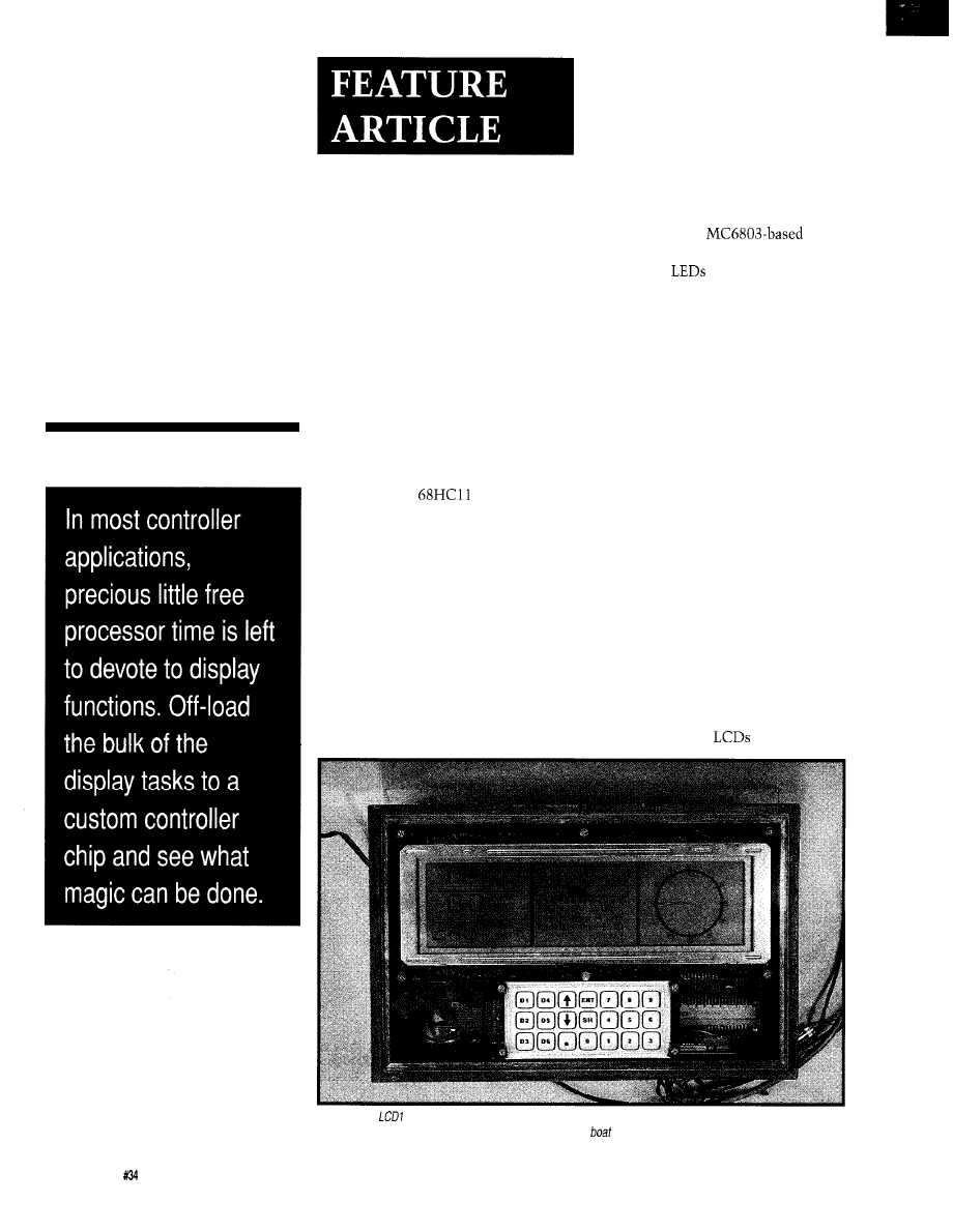
Graphics
LCD Control
for
Embedded
Applications
David Erickson
0
his article
describes my
hardware/software
implementation for a
Graphics LCD display on an embedded
controller. The approach I took
includes the design of a Programmable
Gate Array (PGA) that I use to control
an LCD. I implemented the software
in Small C and
assembly. It
seems to me that just about any
application can be enhanced with a
graphical interface. Many products
already use PC graphics or TV video as
their display. But a lot of these
products are big and tend to stay put in
one place.
I wanted to extend the range of
products that display with graphics to
include low-cost, low-power, and
portable applications. For several years
I have been intrigued by the possibility
of using a graphics LCD display for
such applications. I enjoy building
electronics relating to my sailing and
wind surfing passions. After having
built a few small hardware-only
projects, I was frustrated by having to
repackage the project each time I
wanted to add even simple increments
in functionality. Enter microproces-
sors. Using the power of micropro-
cessors, I built an
weather station with a two-line LCD
readout and
arranged in a circle
to display the wind direction. But
before long, I was frustrated by the
inability to display trends and by the
need to code complex functions in
assembler. I was doing some pretty
heavy stuff in assembler-for a
hardware guy. It was when I began
using lots of pointer math on a CPU
with only one pointer register that my
coding productivity declined-fast. I
gave up on doing anything as ambi-
tious as graphics programming until
I
could do it in C. But buying a C
compiler for a micro was well beyond
my limited budget.
For a while I was tempted to build
systems around PC components just to
use the great development tools. But
PCs and boats don’t get along well:
Disk and keyboard versus salt water,
inadequate power, no easy way to
remote an LCD display, cost.. .the list
goes on.
Then three things happened. Ads
for surplus graphic
began
Photo l--The
custom controller chip makes a sophisticated display possible while using little main processor
overhead. One application for the LCD controller chip is in a
navigation system.
32
Issue May 1993
The Computer Applications Journal
Address
Reg Name
Bits
Range
Description
HPOS
9
W
O-51 1 (O-479 displayed)
Horizontal Pos.
3
8
W
O-255 (O-l 27 displayed)
Vertical Pos.
4
DATA
8
Byte Data
5
OPERATION 3 W
OOO-Pixel ON
Drawing Operation
OFF
Mode
01 O-Pixel XOR
01 l-Unused
OR
101 -Unused
11 O-Byte XOR
11 l-Byte Write
Unused
Table
functions are accessed through a
series
of control
registers. Note
address 2 is available
for future LCD panels
with
more than
256
pixels
Addresses 6
and
7
are a/so unused.
appearing. Motorola made the Small C
Jan. ‘92). I immediately began to
compiler for the
available,
collect the pieces to do my dream
and Circuit Cellar INK published an
project:
a digital display
informative and useful article on the
system for my sailboat.
almost “no money down” was easy,
thanks to Motorola. In no time I was
writing in C, using a real debugger (the
Buffalo monitor), and using a modern,
powerful $12.00 micro. I even got the
floating-point math library
(MATH 11)
working!
I purchased an LCD display from
Timeline, an Hitachi
with
480x128 pixels and a separate control-
ler board. Hooking the board up and
getting basic graphics working hap-
pened in a few evenings.
I was on a roll! Starting with
draw, polyline, and characters being
displayed. Then came large font
characters and display of bit-mapped
pictures (created on a real computer).
The application was also doing
well. After about six months of one or
Motorola 68HCll (issue
Dec.
hardware and software tools
for
two evenings a week, I had a digital
CLOCK (CK)
State
15
0
1
2
3
4
5
6
7
6
9
11
12
13
14 15
0
ST1
\
\
\
ST2
ST3
STCO
MEMORY ADDR
MEMORY DATA
Host
Host
HOST
HOST
0,240
HOST
HOST 64,240
HOST
HOST 0,240
HOST
HOST 64,240
HOST
8 , 0
RH
RH RV RH RV RH RV RH RV RH RV WH RV RH RV
RV
SHIFTER 0 DATA
X
0
4. 0
5. 0
6. 0
0
SHIFTER DATA
X
X
240.0
241. 0
244.0
246.0
SHIFTER 2 DATA
X
X
X
0, 64
64
2. 64
3, 64
4, 64
5, 64
SHIFTER 3 DATA
X
X
X
X
240. 84
243.64
244.64
LCDH
\
MEMORY
MEMORY
The Computer Applications Journal
Issue
May 1993
3 3
compass, display of wind speed and
direction, boat speed, distance, battery
voltage, and a few other bells and
whistles.
maiden voyage was
a two-week trip to Maine during
which it helped us to navigate in the
fog (to the island where we sat out
hurricane Bob, but that’s another
story].
LCD CONTROLLER WOES
Having a winter between sailing
seasons to dream up ways to improve
I was nagged by deficiencies
in the LCD controller. Although
adequate for now, there were several
faults. The only available controller for
the
display uses two Hitachi
61830 chips plus four
This is
available neatly packaged on a PC
board which has a standard eight-bit
interface that ties in easily to any
micro.
There are problems with this
arrangement, though. Each chip
controls one half (left or right] of the
panel. This makes graphics operations
painfully slow. For instance, to write a
single pixel, first figure out which chip
to access by seeing if is greater than
239. Then calculate the memory
address using the formula
x
[H and send it to the chip. Then
send the three least-significant bits of
H
to the pixel to set or clear the
register depending upon whether you
want to turn the pixel on or off. Each
write to the chip requires you to first
write to the control register and then
to the data register (similar to an
alphanumeric LCD]. The grand total
for this single pixel is 29 assembly
instructions to write a byte and 37 to
write a pixel, including an eight-bit
multiply.
As I explored the LCD panel and
controller market, I discovered that
each panel manufacturer has either its
own, or recommended a unique,
controller. The LCD control signals
are similar but different between
manufacturers and even between
generations from a single manufac-
turer. Every controller has a different
host interface and uses different
software. Some controllers use direct
memory mapping and therefore tie up
significant memory space on a 16-bit
address bus. There is almost no
consistency between chips or LCD
panels. It became clear that as a user of
surplus
I would be switching
software, hardware, and packaging
often. This prospect did not seem to be
a pleasant one.
ENTER LCD1
As an avid Programmable Gate
Array (PGA) user at work, I considered
designing an LCD controller chip. In
the past, I have designed Xilinx,
and
chips for several
applications. This was going to be the
first PGA design for my own use,
though.
I call this chip design
The
goals of this design are to arrive at a
low-cost, single-chip (plus RAM),
power LCD controller with an efficient
hardware and software interface for
low-cost microprocessors.
As I was both the hardware and
the software engineer on this project,
and having used an unsatisfactory
controller, I knew exactly what
I
wanted (and didn’t want] for the LCD
controller. First, there should be no
software address mapping. The
I don’t want to find out how can save a lot of money using
ROM-DOS 5 instead of
in our 80x86 product line.
don’t care if ROM-DOS 5 iscompatible with MS-DOS 5 but
costs much less. I like spending much more than I have to.
It makes me feel like a philanthropist and besides Microsoft@
probably needs the money more than I do anyway.
q
Yes,
I want to know the facts about ROM-DOS 5.
Please send me information and a free bootable demo disk to
try with my software.
the
U.S.A. Call Toll
Free
1-800-221-6630
or
fax this coupon to (206)
Name
Company
Address
city
Phone
State
Fax
zip
34
Issue
May 1993
The Computer Applications Journal
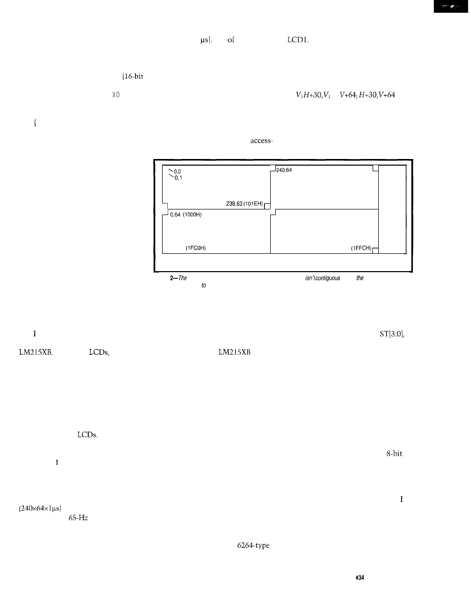
controller should be programmed
directly in terms of H and V. Second,
registers should be directly mapped to
the host. Registers that are greater
than eight bits should appear as two
contiguous bytes so that a STAD
write) instruction can be used. Pixel
drawing operations (SET, C LR, R)
should be done in hardware. Pixels are
to be written by setting a drawing
mode S ET, C L R, X 0 R) and then feeding
the H and V coordinates to the control-
ler. The pixel writes are triggered by
the H address being written. Bytes are
written by setting a drawing mode and
then feeding H and V coordinates and
bytes of data to the controller. Data
writes are triggered by the data being
written. Operations should be fast
enough so that no waiting for a status
flag is required. Table 1 contains the
register set I settled on. Address 2 is
available for future LCD panels with
more than 256 vertical pixels.
An additional goal is that future
LCD panels should use the same
hardware and software interface. I
change panels so seldom that design-
ing new timing circuitry should be all
that is required to support a new LCD.
START WITH THE MEMORY
TIMING
began the design of the basic
memory cycle to support the
Like most
the
interface consists of a clock, H and V
syncs, and data. The challenge with
using this panel is that each of the four
data wires drives one of the four
quadrants on the panel. Each quadrant
can be thought of as a 240x64 pixel
raster for a total of 480x128 pixels.
There is no horizontal or vertical
blanking on most
Simply
output an H sync for every 240 clocks,
and a V sync for each 64 H syncs.
Figure shows the memory and
LCD data path timing. The LCD clock
frequency recommended by Hitachi is
roughly 1 MHz. This clock frequency
allows the LCD to be refreshed every
15.3 ms, which is
equivalent to a
sweep. Since
four bits are output each microsecond,
the total data rate the LCD needs is 4
megabits per second. By reading eight
bits at a time from a single SRAM, this
requires an access once every two
Figure 3 is the block diagram for
clock cycles (2
One my require-
The video-address logic is
ments is to have no-waiting-host
implemented with two counters: 30
performance. Since pixel operations
states for H and 64 states for V. Since
require that memory be read, modified,
the LCD requires that data be read out
and then written to the display, I
of four quadrants at a time, I used
settled on a memory cycle time of 500
adders to calculate the addresses. Bytes
ns with every alternate cycle used for
H,
H,
are
video refresh and host access. This is
read from memory in four successive
twice the minimum requirement for
video memory cycles. To add 30 to the
the video port and allows a pixel write
H count, I used a five-bit adder. To add
operation to happen in four cycles or a
64 to V, I simply set bit six to a 1. Both
respectable 2 us. The memory
the H and V counters are synchronous.
time requirement is a lethargic 300 ns.
H is five bits, V is six bits,
(OOOOH)
(101
EH)
479,0 (003BH)
(0040H)
UNUSED
MEMORY
0,127 (OFCOH)
479,0 (001 EH)
, 0,127
LCD Pixel Addressing
479,128
Figure
LCD display is
broken info four sections, so memory
across entire display,
making pixel address memory address translation difficult.
Going faster is a possibility, but would
cost some additional power.
ADD THE ADDRESSING
Figure 2 shows how pixels are
mapped in memory. The most difficult
part about using the
display
is its arrangement of four quadrants.
To output four bits of data to the
display, the bits must be read from
four different parts of memory. This
reading could be done in software by
making the host addressing more
complicated, but one of my goals was
to simplify host addressing.
I chose to bite the bullet and do
the video addressing in hardware.
Since the LCD is 480 pixels across, I
used 512 bits (64 bytes] per line,
wasting the 32 pixels at the end of
each line. By making a display line a
binary multiple, the vertical and
horizontal addressing can be directly
wired into the address lines of the
RAM. There are 64 bytes, or six
address lines, for H and 128 bytes, or
seven wires, for V. The total is 13 lines
or 8 Kbytes total. A single
SRAM does nicely.
Figure 1 is a timing diagram for
one set of memory cycles. After every
sixteen clock cycles, or eight pixels,
the H address is incremented. The
sixteen cycles are defined by
which is a state counter. This is
implemented as a synchronous four-bit
up-counter with a carry out. The carry
out enables the H counter to incre-
ment. All the memory and data path
control signals are decoded off this
counter.
SERIALIZE THE PIXELS
Each quadrant needs serial pixels,
but the data comes out of the RAM
eight consecutive pixels at a time in
parallel. Originally, I used four
parallel-in, serial-out shift registers.
Each shift register was loaded once
every eight pixel times in sequence.
Because the data from all four shift
registers is needed simultaneously,
used three D flip-flops to delay the
output of the first register, two for the
second, one for the third, and none for
the fourth.
Later on in the project, in a gate
reduction frenzy, I used up the spare
The Computer Applications Journal
Issue
May 1993
35
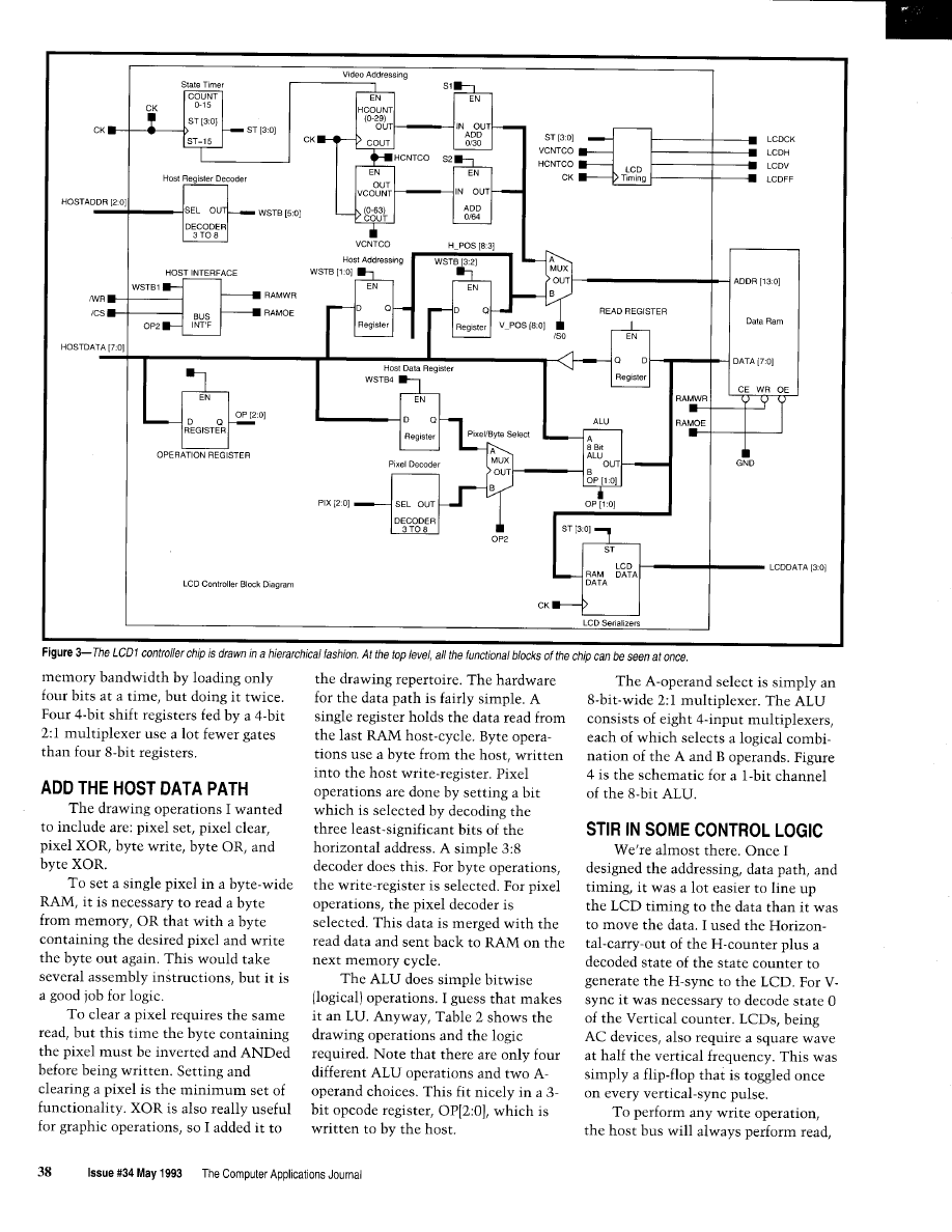
Drawing operation
A operand
B operand
Logical Operation
Pixel set
Pixel clear
Pixel XOR
Byte WRITE
Byte OR
Byte XOR
Decode
Read Data
Decode
Read Data
NOT A AND B
Decode
Read Data
Host Write Data
Don’t care
A
Host Write Data
Read Data
Host Write Data
Read Data
controller
chip.
modify, and write cycles. This required
a simple state machine to receive an
initiation pulse, synchronize it, then
read the RAM, wait for the ALU to do
its thing, and write the RAM. Reads of
the RAM are performed every host
memory-cycle that is not a write cycle.
This way, the Read data register
always contains the byte pointed to by
the latest writes to the HPOS and
VPOS registers. The state machine
controls the data transceiver and the
RAM’s output enable and write lines.
The host write-cycle is triggered on
writes of the H-position register for
pixel reads. For byte reads, it is
triggered on data-register writes.
Table
typical drawing operation can be directly translated a logical operation to be performed within the
THE CHIP AND THE TOOLS
My desire to use a single,
cost, low-power device led me to use
Actel. Xilinx
are RAM based and
require an
to hold their
configuration data. Their advantages
include that they are low power and
can be reprogrammed by changing the
PROM.
MAX family chips are
great for very high speed work, but like
most fuse-based logic, they are fairly
power hungry.
Running at only 2 MHz, speed is a
nonissue. I regularly squeeze 10 and 20
MHz out of these devices. In fact, not
having to worry much about speed is a
luxury that makes designing a plea-
sure. To see if the design would fit in
an Actel Chip, I drew a block diagram
and began adding up logic modules.
My initial module count estimate was
350. The Al010 has 295 and the A1020
has 525. Unless I was way off, it would
easily fit in the larger of Actel’s first
generation devices, the A1020. I might
even be able to squeeze it into the
lower-cost
Actel, like Xilinx, offers different
density chips in the same package. In
this case, both chips come in a
PLCC and have identical
Perfect.
Each Actel logic module is
equivalent to between one and three
two-input gates. It takes one module
to build a latch and two to build a D
flip-flop. Examples of things that can
be made of one cell are: an XOR
followed by a NAND, a two- or
input multiplexer, or a D-latch.
Examples of things that can be made
from two cells are: a D-type flip-flop
with enable, a D-flop with a two-input
multiplexer on the D input, or a J-K
flip-flop. A 74161 counter costs about
Embedded PC
l
256K
Memo& (up to
640K)
l
32K
BIOS ROM
l
Keyboard Port-Speaker Port
For more information please call:
125 Wendell Ave., Weston, Ont.
Fax: (416)
The Computer Applications Journal
Issue
May 1993
39
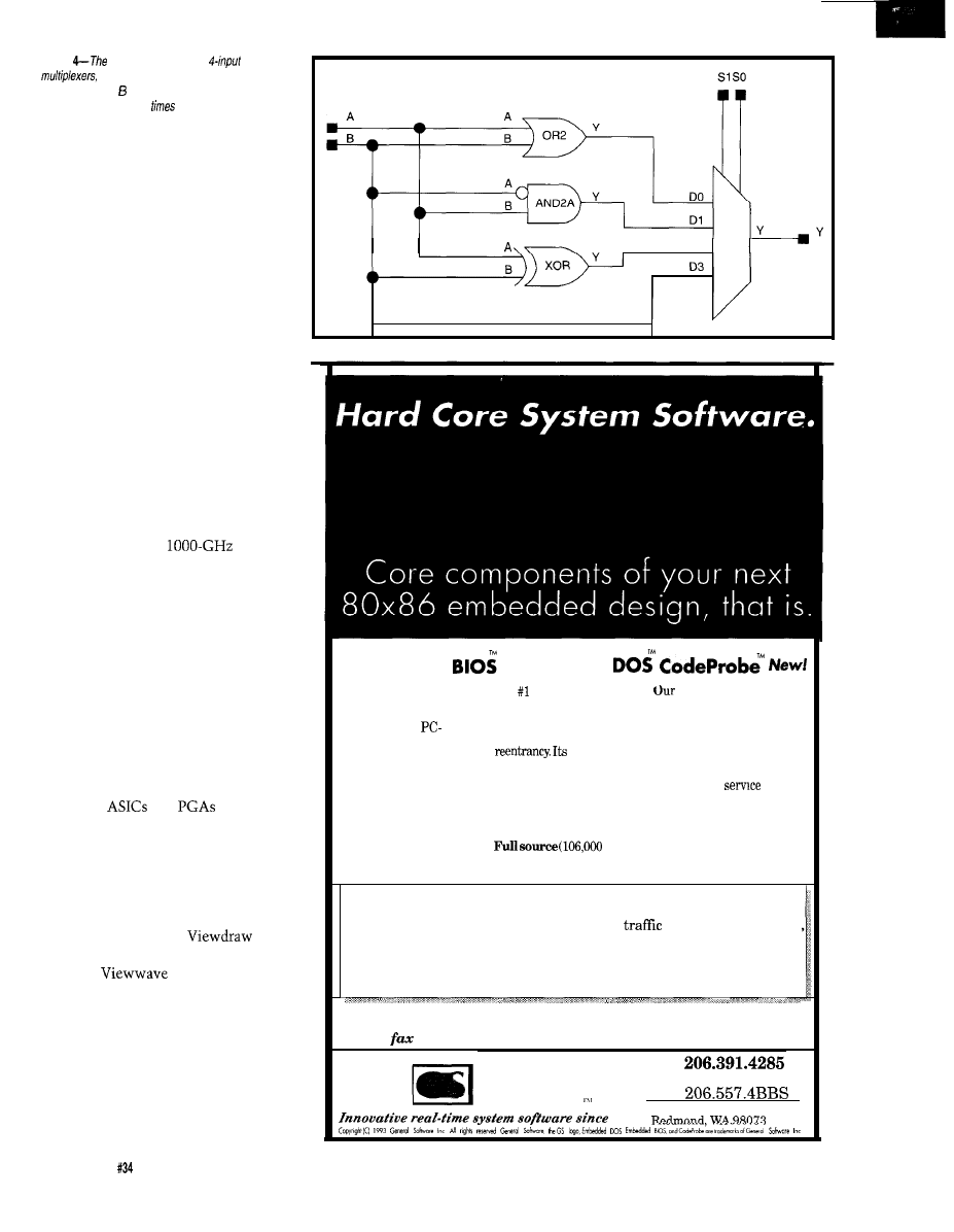
Figure
ALU consists of eight
each of which selects a logical combina-
tion of the A and operands. A l-bit channel of the
ALU is
duplicated eight
for the final unit.
20
cells. Because latches are twice as
efficient as flops, I used them for the
control registers.
Actel meets the single-chip and
low-power requirements, but logic
mistakes cost about $30.00 each: the
chips are not reprogrammable. I used
logic simulation to debug the chip’s
functionality before programming one.
As a result, it took only three tries to
get the hardware working perfectly.
The remaining fifty tries were done
with the simulator. Had I simulated
both the memory and the LCD
controller, I believe I could have saved
a try or two.
The Actel design tools are like
Hardware Heaven: you draw a sche-
matic, simulate the logic, and view
any and all internal nodes on a virtual
logic analyzer with
sam-
pling on infinite channels and infinite
memory. You can place and route the
chip in about 30 minutes, then analyze
the postlayout timing on the same
analyzer. And then, when you are
satisfied with the design, you make a
chip. All this can be done without ever
leaving your PC. This is the way the
world should be. Make your boss buy
you these tools immediately.
I designed the chip using hierar-
chical schematic entry. I consider
hierarchy to be a necessity when
designing
and
with
schematics. I try to put all the I/O pins
on the top sheet and try to make it
look like a block diagram. Then the
details of the blocks go on different
sheets on lower layers of the same
design drawings.
I used Viewlogic’s
for
the schematics, Viewsim for simula-
tion, and
for looking at
signals. At first, I did unit time
simulations. These only consider the
logic states and ignore timing. On an
ASIC or a PGA, the timing simulation
is only accurate after the chip is
routed. Preroute timing numbers are
not very useful because the intercon-
nect delays contribute as much or even
D2
Embedded
Embedded
Our royalty-free
The DOS for
high-performance
Embedded BIOS product
embedded systems, our
software analyzer captures,
turns nonstandard
Embedded DOS operating
time-stamps, and records
hardware into
system supports the entire
hardware interrupts, DOS
compatible computing
MS-DOS API with full
calls, BIOS interrupts, and
engines, even 186 and
built-in
user-defined events in
V-series systems.
high-performance
real-time for later analysis
microkernel supports
Now with over 95
threads, timers, semaphores,
of race conditions? interrupt
activity, and
times.
configuration options, full
source
code (30,000
message ports and queues
An absolute must-have for
and
offers 32,000 levels of
developers involved in
lines), and no royalties,
priority in both preemptive
asynchronous software
Embedded BIOS offers the
debugging. Runs under any
most flexibility, best
and nonpreemptive modes.
lines)
DOS environment with most
control, and lowest price of and reasonable royalties.
real-time kernels.
any BIOS in the world.
Since 1989, we’ve been delivering the core software of the best 80x86
embedded designs. We’ve launched rockets, controlled satellites, flown in
military and commercial avionics, scheduled
lights, rented-out cars
handled bank transations, switched telephone calls, delivered faxes, and
even worked for Uncle Sam, for starters. More and more developers are
turning to General Software for BIOS and DOS solutions that offer the
safety of BIOS and DOS in a high-performance real-time environment.
Call or
for free information and a bootable product demo disk!
GENERAL
T e l
F a x 2 0 6 5 5 7 . 0 7 3 6
SOFTWARE
B B S
P.O. Box 2571
1989
40
Issue May 1993
The Computer Applications Journal
more delay than the gates. Since most
errors are in logic, not in timing, and
since place and route is time consum-
ing (30 minutes versus 2-3 minutes for
a pass of unit time simulation), I used
unit time simulations until I was
happy with the logic. Then I used
postroute timing simulation.
Design rule checking, pin defini-
tion, placing, and routing are done
with Actel’s own ALS tools. ALS also
back-annotates the design with
postroute timing delays. Then I used
Viewsim and
to check the
timing. First, I got the address timing
and control registers working. Then I
tackled the data path and host logic.
Finally, the LCD timing was adjusted
to match the data sheet. I also verified
that the new controller chip matched
the LCD timing of my existing
controller board just to make sure.
I did timing analysis postlayout to
accurately assess whether the chip
would work. Since 98% of the timing
was noncritical, I only looked closely
at two areas: the memory write-pulse
timing and the long-ripple-carry-chain
of the counters. I used the Actel ALS
delay generator to analyze the delays
from the Q-output of each flip-flop,
through every possible logic path, and
then the D-input of each flip-flop. This
tool is excellent at answering the
question, “How fast will it run?” The
result was that the carry-chain was
indeed the worst path. It came in at
ns with worst-case temperature,
voltage, and process. This means the
chip will clock at 7.7 MHz, well in
excess of the required 2 MHz. This
number could be significantly im-
proved if I designed for speed instead of
to minimize the gate count. The
pulse timing was important because
I
used a gated clock to generate this
signal. I wanted to verify that the
write-pulse fell only after the address
was stable and it rose again while the
data was still stable. I verified this by
looking at the waveforms generated by
using the postlayout timing numbers.
THE APPLICATION CIRCUIT
As Figure 5 shows, the schematic
of the application circuit is quite
simple. The host bus consists of an
bit data bus, a
address bus, a read/
write control line, and a chip select.
The clock inputs can be connected to
any convenient source of 2 MHz
If unavailable, a
crystal
and a few
can be used along
with an on-chip inverter to make an
oscillator. The
clock is fed into
the two clock inputs. There are two
clock-input pins because the clock
input on an Actel can only drive clock
pins on flip-flops. I needed to use the
clock through some gating logic to
make the SRAM write-pulse. I used a
single
SRAM as the video
memory for a display with a resolution
of 480x128 pixels. The higher address
lines are for future use.
The host bus interface connects
easily to a microprocessor. All read
and write operations occur on the chip
select
signal. For a
processor, simply gate the desired
address match with E to make
For
Intel buses with separate write and
read signals, additional gates are
needed. The read/write line (R/W) is
Plus
Lots More...
Embedded
Microcomputer
An upgrade consisting of
a new EPROM, disk, and
manual costs just $60.
Order yours today!
Circuit Cellar, Inc.
4 Park Street, Suite 12
Vernon, CT 06066
Tel:
(203
Fax: (20
The Computer Applications Journal
Issue
May 1993
4 1
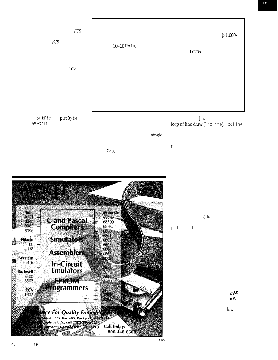
simply low during a write and high
during a read cycle. Address and data
should be stable before and after
on a write cycle. For a read, data comes
out about 50 ns after
goes low.
The MAX635 supplies the -13.5
volts that the LCD needs. I used a trim
pot for R2 to adjust the -13.5 V. I also
use -13.5 for RS-232 drivers and analog
circuitry in lieu of -12 V. The
pot,
R3, controls the LCD contrast and
should be front panel mounted. This
particular LCD display is quite
temperature sensitive, so R3 may
require frequent adjustment.
GRAPHICS SOFTWARE
I wrote all the graphics routines as
C functions.
and
are
written in
assembly language
for speed. Table 3 is a list of the
graphics functions.
Small characters, zoomed (large)
characters, and rectangular bitblit
operations are all done on byte
boundaries for simplicity and speed.
I
have no particular need for propor-
tional fonts. In fact, even at the
Price and Tool Update
Actel 1010 chips are now available for under $10 in very large
piece) quantities. Considering that a 1010 replaces about 30-50 TTL devices
or about
the pricing is quite appealing. Small-quantity prices
are proportionately down. With surplus graphics
in the $lO-$25 range
and current SRAM prices, the cost of adding graphics to a project can be
minimal. The 1020 has 80% more gates, and other parts with much higher
densities are also available.
Actel has announced a low-cost development system for their smaller
devices. Logic simulation using Viewlogic is still fairly expensive, but
another design option is available. Each Actel chip has four pins allocated to
a “probe” function. A simple interface to a PC is available that will allow
the you to select any internal node of the IC to be brought out on two
“probe” pins. This way, the innards of the chip can be observed. I haven’t
used this myself, but Actel recommends it.
hardware level, writing a byte to the
Pixel draw
Pi
X
)
is in the inner
display simply ignores the three least-
significant bits of the horizontal
is based on Bresneham’s algorithm. It
register. They are used only for
could be significantly faster if written
pixel operations. Characters and blits
in assembly. Lc d L i n e is used by
can be written starting on any line.
I
o 1 y L i n e to draw complex shapes out
chose a
font with two-line
of connected lines. The parameter list
descenders. This provides one pixel
is a pointer to a list of X,Y points. It
between characters if the characters
draws until it comes across an illegal X
are on byte boundaries.
value.
Microsoft Flight Simulator was
partly responsible for my motivation
to build attractive gauges. I draw them
on an X-Windows system using the
b i t ma p command of the X-Windows
icon editor. It conveniently outputs a
static data array in C source format
that can be simply included in your
source. It even has
f
i n es for the X
and Y sizes that I simply pass to
u Re c
It couldn’t be much simpler.
I guess a converter could be written to
convert the output of any available
drawing tool that outputs bit-mapped
data. Remember that the least-
significant bit is the leftmost pixel of
the display.
CONCLUSION
Building the LCD controller and
my application was great fun. I feel
satisfied that I met all my goals. The
power dissipation measured 80
for
the LCD panel and another 80
for
the controller chip and the SRAM.
That’s about the same as one
power bipolar PAL. The drawing
performance is fast enough for my
application. Most of the screen,
consisting of 24x30 pixel zoomed
Issue
May
1993
The Computer Applications Journal
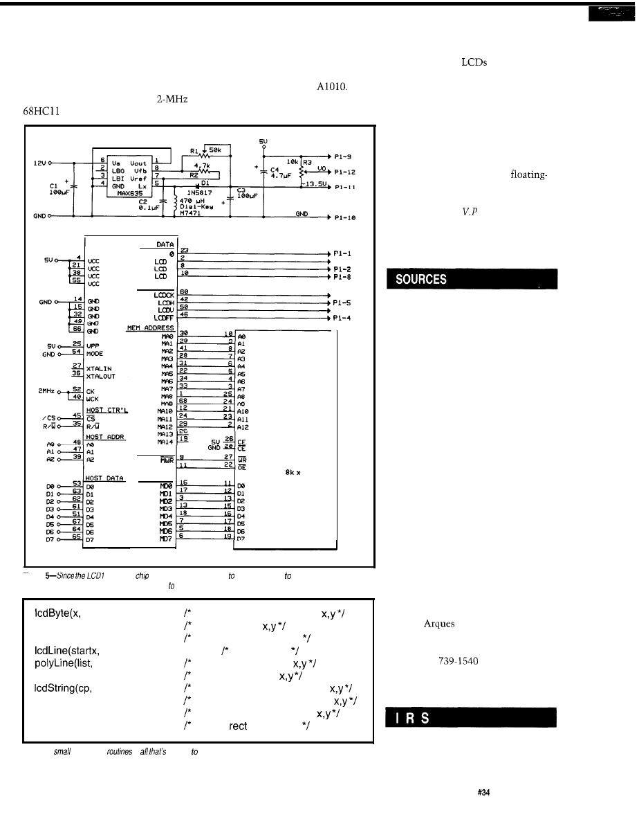
characters plus three lines of small
and processing data. After getting the
characters, is updated once per second,
first controller chip working,
I
was
with a gauge needle and two moving
ultimately able to squeeze the design
bar indicators updated twice per
into the lower-cost Actel
This
second. All this is done with a
required that I reduce away some
which is also busy collecting
unnecessary logic and make some
LCD
LCD
1
2
3
LCD CTR’L
MEM CTR’L
MOE
MEM DATA
SRAM
8
6 2 6 4
P l - 7
P l - 6
Pl-3
Figure
controller
was designed specifically connect directly a microprocessor bus and
an LCD display, additional components are kept a minimum.
y, i)
Writes a byte to the LCD at
putPix(x, y)
Puts a pixel at
setGrMode(mode)
Sets the drawing mode
starty, endx, endy)
Draws a line
x, y)
Polyline beginning at
IcdChar(i,x,y)
Put a character at
x, y)
Output a string to the LCD at
bigChar(ch,x,y, z)
Put a zoomed character (z) at
bigString(cp, x, y, z)
Output a zoomed string at
putRect(ptr, x, y, xsiz, ysiz)
Write a
to the LCD
Table 3-A
library of C
is
needed develop applications fhaf use fhe LCD display
controller.
speed versus gate count tradeoffs.
Since most other
have simpler
interfaces, controllers for them should
also easily fit in the smaller device. I
look forward to designing another chip
to support another LCD for another
project. That will be the final test of
my portability goals.
My current application is 28K and
growing, including a font table, icons,
the graphics library, and the
point math library.
q
Dave Erickson is
of Hardware
Engineering at Datacube, where 10
MHz is considered DC.
The schematic, symbol, and Actel
files for the chip, plus the source
code for the graphics library are all
available on the Circuit Cellar BBS.
So are Epson-80 printable schematic
files for the chip for those interested
in the details. The schematic files
can be used to change the design or
to retarget it.
I will supply LCD controller chips
(plus a terse data sheet) to interested
parties for $35.00 each. Send a
check to: David Erickson, 6 Oak
Drive, Topsfield, MA 01983.
The chip design is copyrighted. I ask
that users treat it like freeware. You
may make copies of the chip,
modify it in any way you like, or
design it into your embedded
control product for resale. I only ask
that you do not sell the chip alone
or sell an LCD controller board
based on it without my permission.
Actel Corp.
955 E.
Ave.
Sunnyvale, CA 94086
(408) 739-1010
Fax: (408)
407
Very Useful
408 Moderately Useful
409 Not Useful
The Computer Applications Journal
Issue
May 1993
4 3
Firmware Furnace
Ed Nisley
From the Bench
Silicon Update
Embedded Techniques
Patent Talk
Time: The ‘386SX
Project Gains a Timer
ing that light travels about one foot in
one nanosecond. Those wires (now
collector’s items, of course) helped her
put electronic speeds on a human
scale:
that’s
what 70 ns means!”
It turns out that wired signals
travel at about one-third the speed of
light in vacuum, so one nanosecond is
about four inches. One of the wait
states I discussed last month reaches
to the far wall of your domicile, a
bit I/O access stretches across the
street, and an
access ends well
down the block.
In this column, 1’11 add an
8254 timer chip to the Firmware
Development Board described last
month, explore more ISA bus timing
issues, and introduce a handy BIOS
timing facility you may not have met
before.
Keep Admiral Hopper’s wires in
m i n d . .
WHERE DOES TIME
COME FROM?
Timing on PC-class machines has
always been a problem because the
facilities are only slightly above
rudimentary. The system board
includes three timers (in an 8254 or in
44
Issue May 1993
The Computer Applications Journal
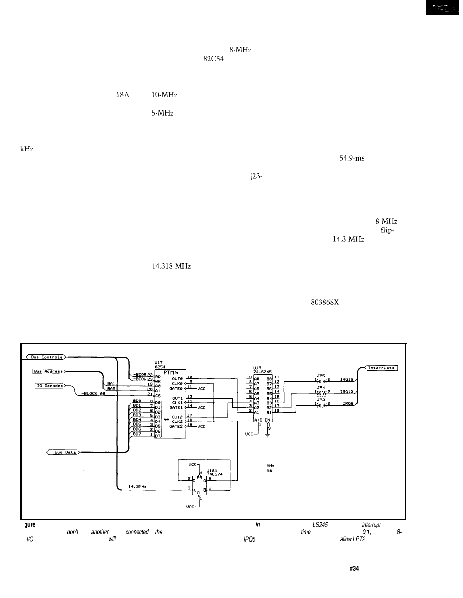
a smidge of LSI), but only one channel
can generate an interrupt. Worse, that
timer is tied into such diverse features
as the BIOS time-of-day routine and
the diskette motor turn-off delay, so
tinkering with it can be hazardous to
your program’s health.
The AT added an MC1468
real-time clock to keep track of the
date and time while the system power
is off. The chip (or its moral equivalent
in LSI) can produce periodic interrupts
on IRQ 8 at rates ranging from 8192
to 2 Hz. The BIOS implements an
alarm clock function based on that
interrupt, which will come in handy
for the code this month.
While it’s possible to use the PC
timers in your code, they are best left
for the normal BIOS services (unless,
of course, you aren’t using the BIOS
services, in which case all the hard-
ware is fair game). I decided to add a
separate 8254 timer chip to support
some upcoming projects, but we’ll put
the standard PC facilities to good use,
too.
Figure 1 shows the three chips
needed for the timer circuit. Of course,
you’ll also need the buffering and
address decoding logic from last
month, but the extra aggravation is
fairly small. Photo 1 shows the proto-
type card with the circuitry thus far.
The 8254 timer is identical to the
one used on the original AT system
board and is rated for an
clock.
You may use an
CMOS version
if one is available, as the specs are
essentially identical. A -2 suffix
indicates that the chip can handle a
clock and has a slightly faster
bus interface. A -5 suffix brands it as a
dud that won’t work in this
circuit. The suffixes don’t make sense,
these chips were born back in the bad
old days before rational “dash”
numbers appeared.
Although It Would Be Nice to
have a sensible clock frequency, I
decided to use the 14.318MHz
foot) signal from the ISA bus connec-
tor. Pardon the digression, but I have
to explain why these frequencies are
what they are.
The PC’s designers used an 8284A
clock generator, which divides its
crystal oscillator frequency by three to
produce the 8088’s CPU clock. The
Color Graphics Adapter needed a
signal to produce its
composite video signal, so why not put
a (cheap) 14.318MHz crystal on the
8284 and drive the CPU at 4.77 MHz?
The 8284 also produces a PCLK
output at half the CPU clock rate, or
2.39 MHz. The PC’s 8253-5 timer chip
could handle that rate (it went all the
way up to a blazing 2.6 MHz), but the
maximum interrupt rate would then
be 27.5 ms, which was a bit peppy for a
CPU that could execute perhaps 8,000
instructions in that time. Dividing
PCLK by two produces 1.19 MHz,
which the 8253 then divides by 64K to
generate an interrupt every 54.9 ms.
The rest, as they say, is history.
When the AT came along, it
would have been possible to boost the
BIOS tick rate to take advantage of the
new-and-improved 80286 CPU’s
horsepower, but too many programs
depended on that
rate. Only a
whole new operating system can
change the clock rate; anything less is
chained by historical necessity.
But, even though the PC’s bar-
nacles limit the system board 8254 to
1.19 MHz, we have no such restric-
tion. The 8254 is rated for an
clock, so I used half of an LS74
flop to chop the
signal down
to 7.16 MHz.
Thus, each of the three timer
outputs can produce rates from about
140 ns to 9.15 ms under firmware
control. Admittedly, the faster rates
aren’t particularly useful, since even a
40-MHz
CPU can’t accom-
plish much in 140 ns, but the im-
proved resolution is still a Good
Thing.
7 . 1 5 9 1
1 3 9 . 6 8
l--The 8254 timer chip shown here uses the address decoding and bus buffering circuitry presented last month’s issue. The
chip drives the
request
es; make sure you
have
device
to same lines. In order to ensure sufficient interrupt acknowledge
timers must use Mode or 3. Using
bif accesses or additional waif states
ensure enough time for 8254 accesses. Also, if you select
for use by the timer, be sure you don’f
elsewhere in the
system to use the same interrupt.
The Computer Applications Journal
Issue
May 1993
4.5
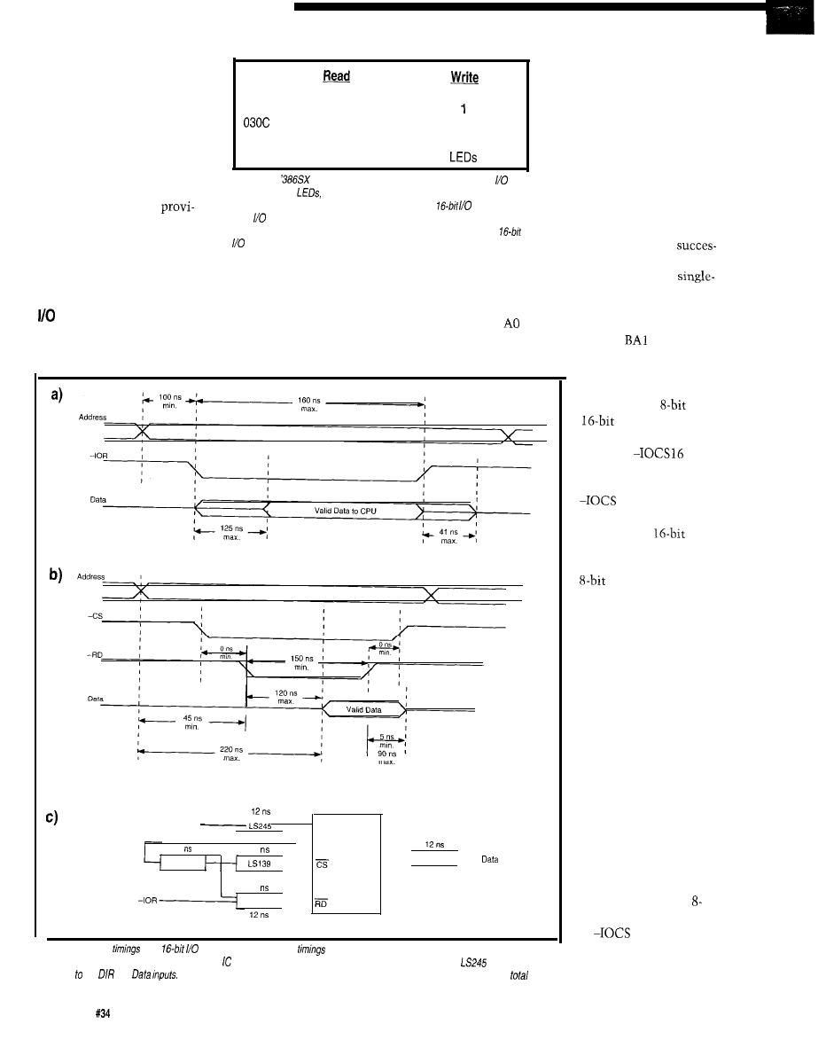
All three outputs drive
interrupt request lines on the
port
connected. The hardware
ISA bus connector through a
0308
Timer 0 Count/Status
Timer 0 Count
ignores the high byte during
LS245 which serves as a buffer.
030A Timer 1 Count/Status
Timer Count
writes and the firmware must
I’ll assume that you’re building
Timer 2 Count/Status
Timer 2 Count
ignore the high byte during
this board for a specific reason,
030E
nothing
Timer Control Register
reads. Table 1 shows how
and that you’ll build the
031 E
Switches
devices and their ports are
hardware based on your
mapped in the address space.
requirements. With this in
Table l-The
Firmware Development Board now has three
devices: sixteen
a matching set of DIP switches, and the 8254 timer.
The 8254 has four internal
mind, I have made no
Because the address decode logic was designed for
accesses,
addresses that are normally
sions to disable the interrupts
each port must appear at an even address. The timer has four infernal
accessed as successive I/O
with software. If your project
registers fhaf are mapped into the low-order byte of four consecutive
ports. On this board, however,
requires interrupts, then you’ll
ports.
they must be located at
want to install jumpers for selecting
16-bit I/O operations based at even
sive even addresses, because the
IRQ lines.
address boundaries, but you don’t have
decoding logic cannot handle a
byte read or write at an odd address. As
ADDRESSING
to connect an I/O device to each and
you
can see from Figure 1, the 8254’s
The Firmware Development
every data bit. For this case, the 8254
is wired to the low-order byte of the
and Al inputs are driven by the
Board’s address decoding logic assumes
data bus and the high-order byte is not
buffered address lines
and BA2,
respectively.
A d d r e s s
,
AO. Al
11
38
8254
F521
Data
LS245
40
LS245
Figure 2-(a) ISA bus
for a
read operation. (b) 8254
for a read operation. (c) Simplified Firmware Development
Board schematic showing fhe delay through each involved in a read operation. The two values shown for the
in the data path
correspond the
and
The delays shown in (a) must be added to the total delays along each path to find the
times.
4 6
Issue
May 1993
The Computer Applications Journal
As I mentioned last
month, the only differ-
ence between
and
I/O operations is
that the expansion board
activates
to
indicate that it can
handle both bytes. If
16 remains
inactive, the system
board breaks
operations into a
sequence of two separate
accesses by writing
the low-order byte to the
first address and the
high-order byte to the
next address.
The system board
swaps the bytes around
SO
that the bytes wind
up at the correct I/O
locations, but the
Firmware Development
Board does not include
the circuitry to handle
its end of this dance. As
I mentioned last month,
if you must support all
possible I/O accesses,
check the references for
the details.
However, if the
CPU is executing an
bit operation, it ignores
the
16 signal and
simply writes the byte
to the specified address.
Because the 8254 is
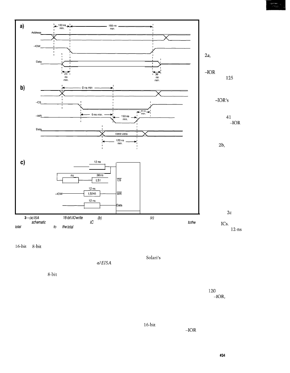
Valid Data from CPU
Address
Address
11
F521
Data
LS245
39
LS245
AO, Al
a254
Figure
bus timings for a
operation. 8254 timings for a write operation. Simplified Firmware Develop
menf Board
showing the delay through each involved in a write operation. The delays shown in (a) must be added
delays along each path find
times.
Figure shows the
delay times for some of
the key
The LS245
connected to the low-order byte of the
bus, it will respond correctly to either
or
I/O operations directed
to even addresses. The high-order byte
will be mush, but in this case we don’t
care.
must be able to interpret the hardware
specs, even if it’s only to point out
bugs that the hardware folks get to fix!
The only other difference is in the
bus timing, with
I/O operations
requiring twice as many cycles. As it
turns out, those extra cycles are
critical to using the 8254.
The timing values and diagrams in
this column are based on
ISA
Theory and Operation, which
replaces his earlier AT Bus Design I
mentioned in issue 3 1. The new book
is $90 from Annabooks and is essential
if you’re doing this stuff, but I wish it
were paperbound and a lot less
expensive. They do toss in a copy of
their XT-AT Handbook, which is a
shirt-pocket sized compendium of PC
information.
buffers add a
(three
foot!) delay to the address lines on the
input and another 12 ns on the data
output side, so the time between a
valid address and valid data on the bus
is really 244 ns. Comparing that with
Figure 2a tells you that this just isn’t
going to work.
TIMING FROM BOTH SIDES
Because the 8254 is the first
nontrivial I/O device on the Firmware
Development Board, it’s worth going
into some of the details needed to
ensure that it will actually work. This
still isn’t a hardware column, but if
you’re in the firmware business, you
diagrams, the horizontal
time axis is not drawn to
scale, so you can’t
compare things just by
looking.
According to Figure
the ISA bus address
settles at least 100 ns
(just over 30 feet) before
goes active. No
more than
ns later,
the data from the card
must become valid and
it must remain valid
until
trailing
edge. The data drivers
must not remain active
more than ns [a mere
14 feet) after
goes
inactive to prevent bus
contention.
As you can see in
Figure
the 8254’s
output doesn’t become
valid until 220 ns after
the address stabilizes, or
120 ns after the begin-
ning of the -RD pulse,
whichever is later. This
may look close enough,
but remember that the
8254 isn’t directly
connected to the ISA
bus!
Figure 2a shows the (considerably
simplified) timings for a
ISA I/O
bus read. Figure 2b shows the corre-
sponding timings for the 8254’s read
operation. As is traditional in these
This situation is precisely the
reason why wait states were invented.
Recall from last month that a single
wait state adds
ns (about 40 feet]
to the duration of
which is
enough to allow the 8254’s data to
arrive and settle down.
There are several other paths
through the logic that need checking,
such as the address to -CS time versus
the
to -RD times. In order to be
sure the chip will work, you must
analyze all the paths and add up the
The Computer Applications Journal
Issue
May 1993
4 7
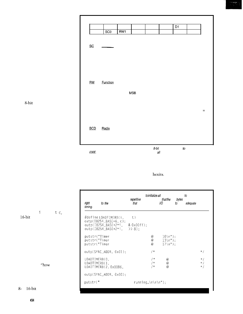
timings. Hint: even if you do the New
York Times crossword in pen, use a
pencil on this job!
Obviously, if you do a lot of this
you’ll depend on an automated timing
analysis program that checks every
path in your schematic using built-in
delay tables for each IC. It’s expensive,
but better you should find problems
before the board goes into production
than suffer the slings and arrows of
outrageous glitches in a “finished
product.”
As an exercise, work though the
write cycle diagrams shown in Figure 3
to see if an additional 40 feet of wait
state will suffice here, too.
Now, here’s the punch line. If you
use only
I/O operations, the ISA
bus hardware will insert three extra
wait states (about 120 feet) with no
extra effort and no additional circuitry.
Basically, by picking the right I/O
operation, we can tune the system to
work correctly with even this rather
pokey IC!
The down side is that should you
(or someone else, like the poor soul
who maintains the code after you’re
gone) forget about this and decide to
use a 16-bit I/O operation, the card
will fail. Worse yet, the timings are
just close enough that it’s possible
some of the cards will work some of
the time and others won’t work most
of the time!
Try to find that bug!
However, because this column
deals with sharp objects on a regular
basis, I’ll show you how to use the
hardware either way. The checkout
code this month, t
met es
. uses
either
or 8-bit I/O operations.
You have control of the wait state
generator so you can see just how well
your hardware responds.
COUNT THE WAYS...
Although the 8254 is probably
familiar to most readers, I’ll provide a
capsule summary of the way it works
so we will all start from the same
point. A complete
to use the
8254” is well beyond this column’s
charter, but, fortunately for us, we
don’t need all that much detail.
The 8254 contains three indepen-
dent or
counter/timer
The Control Word bit names are:
D7
D6
D5
D4
D3
D2
DO
SC1
RWO M2
M l
MO
BCD
The SC bits select the Counter channel:
Function
0
Counter 0
1
Counter 1
2
Counter 2
3
used for Read-Back commands
The RW bits specify the data for each counter. The counters are always 16 bits wide,
but you can send one byte in special situations:
Function
0
used for Counter Latch commands
1
Read/write Counter
only
2
. ..LSB only
3
Read/write LSB followed by MSB
The M bits specify the Counter’s operating mode in the usual binary fashion, from 000
Mode 0 to 101 = Mode 5. Specifying Mode 6 or 7 results in Mode 2 or 3, respectively.
The BCD bit selects the counting radix:
Radix
0
Binary, max count FFFF hex
1
BCD, max count 9999 decimal
Figure
4-Each counter channel in the 8254 is configured by an
control word written the Control Regisfer at
address
The Firmware Development Board does not support possible 8254 configurations!
channels, each with three pins: a
complement. If you prefer BCD to
Clock input, a Gate control input, and
binary, you can have them count from
an Output. Unlike 8051 counter/
9999 in decades instead of from FFFF
timers, these gizmos count down, so
in
Honest.
you load them with the number of
The three channels, referred to as
counts you need instead of the two’s
Counters 0 though 2, are all 16-bit
Listing l--This Micro-C
code fragment shows how
three 8254 channels Mode 3. The
#define macro eliminates a good deal of
code and ensures
right
are written
in fhe
sequence
right ports. Note
fhis code uses d-bit operations ensure
bus
c ,
\
t
\
t
0 = 1 ms square wave pin
1 = 2 ms square wave pin
2 = 3 ms square wave pin
sync at start
0x0036, 7159);
1 ms 7.1591 MHz
0x0076, 14318);
2 ms 7.1591 MHz
21477):
3 ms 7.1591 MHz
. timers are now
48
issue
May 1993
The Computer Applications Journal
counters and may run in one of six
different modes, known as
0
through 5. Each mode uses the three
pins in different ways, so you must
match the firmware setup, counter
mode, and external hardware in each
application.
Mode 0 is a simple counter: the
firmware loads a value and the 8254
decrements it by one count on the
falling edge of each clock pulse, as long
as the Gate control remains high. The
Output goes low when the count is
loaded and goes high when the count
hits zero. After that, the counter
continues counting but the output
won’t change. This mode comes in
very handy for generating precise
software delays to match a hardware
gadget because the output can produce
an interrupt with no additional
hardware.
Mode works the same way, but a
rising edge on the Gate input serves as
a trigger and starts the counter. We
can’t use this mode, because all the
Gate inputs are tied high on the
Firmware Development Board.
Mode 2 divides the clock input by
the programmed count value and
produces a single low pulse each time
the count strikes zero. The counter
reloads the initial value and continues
counting, so you get one pulse out for
every Clock pulses in. This is handy
for dividing a frequency by a lh-bit
value, but we won’t use it.
Mode 3 is similar to Mode 2 and is
most useful for producing periodic
interrupts. This is the mode used by
the timer on the system’s mother-
board: the output is a square wave
with a period of clock cycles. The
Gate input can synchronize the
Output’s phase to an external signal,
but the Gate inputs will remain tied
high until
I
can think of something
that I need to synchronize with.
Modes 4 and are basically Modes
0 and 1 with a twist: the Output
remains high until the Count hits
zero, at which point it produces a
single low pulse.
If you plan to use the 8254 with
anything other than a periodic Clock
input, make sure you read the data
sheet
There are several
that stand out only after
Are you looking for a C++ and Standard C cross compiler for DOS or
UNIX, targeting 680x0, i386,
Mips or
Is complete
source code to your compiler important to you?
How about a
complete Standard C library implementation, including floating point?
Hundred Acre Consulting is now
Package includes:
offering GNU C++ and Standard C
support in a number of native and
cross compiler configurations. Hosts
supported include M S / D O S a n d
Windows on a 386 or 486, Sun 3 and
Sun 4 with
4.1.1,
with AIX 3.2, most System V based
UNIX systems, and many
others. Call today for details!
C++ and Standard C compilers.
Remote source-level debugger.
Object file support utilities.
Complete Standard C library.
Library of useful C++ classes.
Binaries and complete sources.
No royalties for redistribution.
One year of support included.
Now works with Windows!
Basic Support Package: $495
Hundred Acre Consulting
Reno NV89502
Phone:+l-702-329-9333
Fax:+l-702-329-9566
BBS:
Only $851 for
The world’s most innovative emulator for members of the
8051
is incredibly affordable. Metotink’s unique
Advanced Emulation Technology
potent pending) delivers
the best possible emulator value for engineers, consultants and
students.
AET is revolutionary design architecture that provides more
features with 75% fewer components, smaller board space and
lower cost. Emulator and probe electronics are integrated in
single pockoge only 3” by 4”.
also delivers leading-edge customer service, including
a 30 day money back guarantee, 10 day trial for qualified
customers, rental plans and free technical support.
Up
to
40 MHZ Dperotion
SUPPORTS 8031/8032'S
Code
Memory
SUPPORTS
64K External
Memory
Windowed User Interface
Hordwore
Serial link to Any PC
Trace Memory
Macro Cross Assembler
Tronsporent Trace
(View
While Executing)
Time Nonintrusive
Symbolic
Level Debug
Built-In
tod
ink
oy
. FREE
ion PO
DEMO
DISK!
(800)
Box
1329
Chandler,
FAX:
926.1
638-2423
85244-l 329
98
The Computer Applications Journal
49
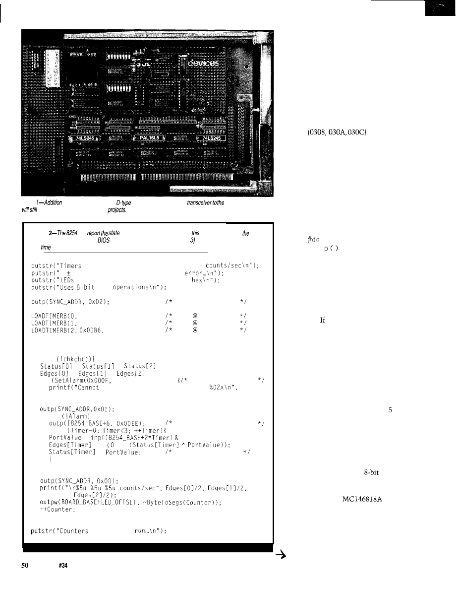
Photo
of an 8254 timer, a dual
flip-flop, and an octal bus
development board
leave adequate space for future
Listing
can
of each Counter’s Output pin, so
routine can display
frequency. The code uses the
alarm clock routine (shown in Listing to measure out one second of
real
while if checks for Counter Output transitions.
should produce 1000, 500, and 333
one or two counts for sampling
display iteration counter in
I/O
0x0036, 7159);
0x0076, 14318);
21477);
Counter = 0;
sync at start
1 ms 7.1591 MHz
2 ms 7.1591 MHz
3 ms 7.1591 MHz
while
=
=
= 0;
=
=
= 0:
if
0x4240, &Alarm))
alarm in 1 second
use BIOS alarm function, code
Alarm);
break:
while
latch all status bytes
for
=
0x0080;
+= !=
=
save for next pass
continue to
you’ve designed the thing into a circuit
and it behaves, well, strangely.
Setting up a Counter channel is
straightforward: write an 8-bit “Con-
trol Word” to the Control Register
which is at address 030E on the
Firmware Development Board. Figure
4 shows the Control Word bit layout.
You must write one Control Word for
each Counter channel, then write one
or two bytes to the Counter channel’s
address
to set the
initial Counter value.
HARDWARE CHECKOUT
Although in the future I may
come up with other applications that
require a wiring change, Mode 3 will
suffice to exercise the hardware and
illustrate the firmware techniques.
Listing 1 shows the code needed to set
up all three counters to produce square
wave outputs.
The
f i n e macro bottles up
the three
out
functions needed to
load the control word and write the
two counter bytes. If space is tight you
can convert this macro to a function
call, but I opted to use this method for
its simplicity.
While that code starts the timers,
you’ll need an oscilloscope to verify
the outputs. you don’t have a ‘scope,
Listing 2 may be of more interest
because it uses the PC to measure and
display the results. If what you see on
the screen is correct, the hardware is
working, but if it fails, you must cadge
a ‘scope from a friend.
The 8254 can return a Status Byte
for each counter that indicates, among
other things, whether the counter’s
Output pin is high or low. Figures
and 6 show the Control Word and
Status Byte values you’ll need. A short
routine can count the number of times
the Output bit flips each second to
calculate and display the output
frequencies of each channel.
(Why do you write an
control
word and read an 8-bit Status Byte!
Because, just because!)
Remember the
I
mentioned earlier? This is where it
comes in handy. BIOS software
Interrupt 0x15 Function 0x83 uses the
periodic interrupt from that chip to set
a delay; when the delay expires, the
Issue
May 1993
The Computer Applications Journal
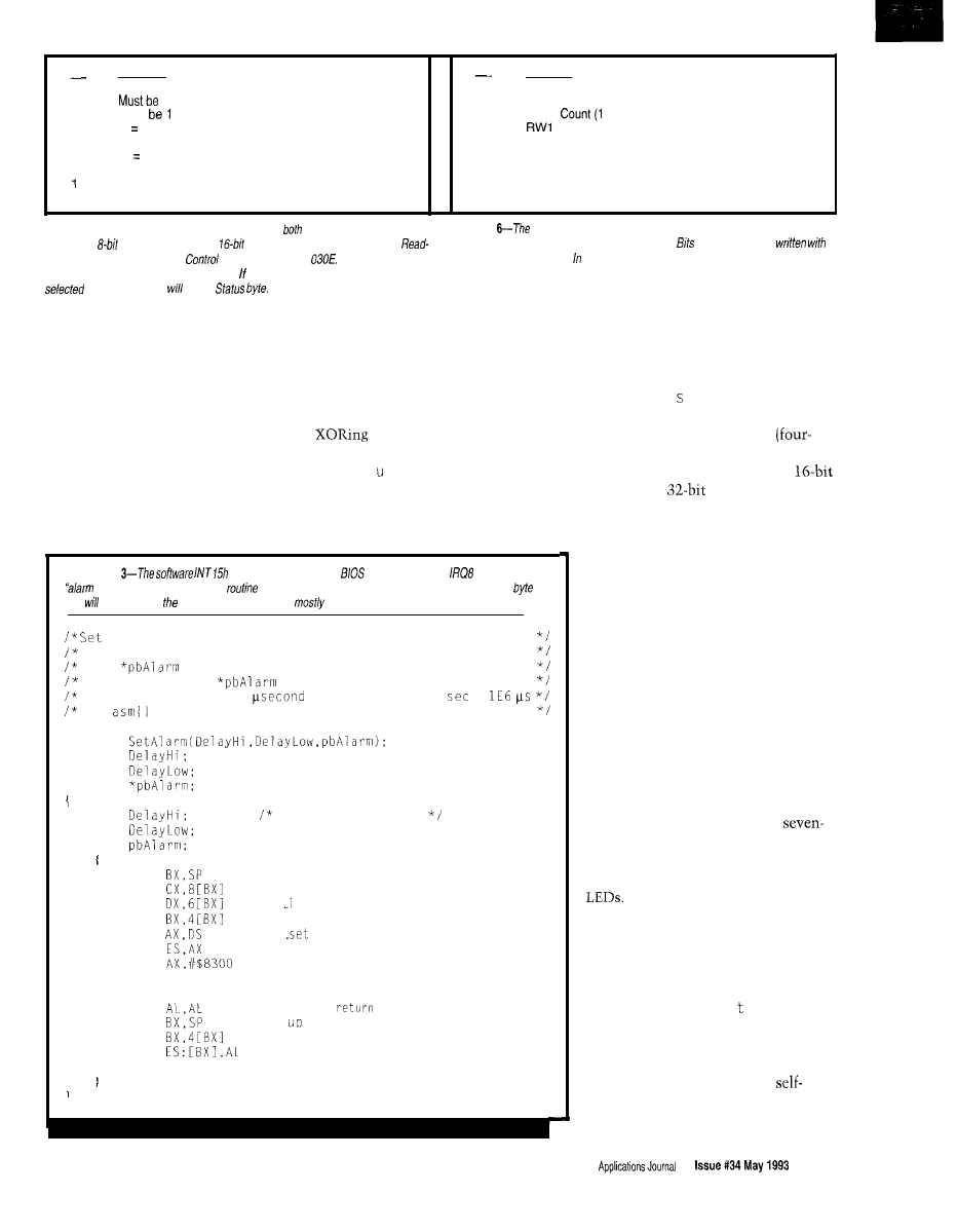
Bit
Function
Bit
Meaninq
7
1
7
State of Output pin (0 = low, 1 = high)
6
Must
6
Null
= not counting, 0 = counter loaded)
5
0 latch current Countofselected Counter channels
5
4
0 = latch current Status of selected Counter channels
4
R W O
3
1 select Counter2
3
M2
2
1 = select Counter 1
2
Ml
1 = select Counter 0
1
MO
0
Must
be0
0
BCD
Figure &-The 8254 includes latches that capture
bytes of the counters, so two
successive
reads can return valid
data. The latches are activated by
Back Commands written to the
Register at address
Note that you can
latch a// three counters with one command. bit 4 is zero, the first byte read from the
Figure
status byte read back from the counter channels gives you enough
information to figure out what the counter is doing.
5-O echo fhe bits
the counter’s Control Word. fhe code for this column, on/y bit 7 is useful.
Counter channels
be the
interrupt handler flips bit 7 in the byte
of your choice. This relieves your code
of the need to worry about interrupts
because, after you set the alarm, you
simply test the target byte.
The code in Listing 2 sets up the
three 8254 timers with periods of 1, 2,
and 3 ms, then enters a loop that will
end when you press a key. Until then,
it sets up a one-second alarm and
enters an inner loop that latches and
reads back the current status for each
channel. The 8254 latches all three
channels at once, but the Status Bytes
must be fetched with three separate
read operations.
Determining when each Output
pin changes is a simple matter of
the current state with its
value during the previous iteration.
The St
at s
array holds that state
information for each timer, while the
Ed g e s array is incremented on each
change.
Listing
Function 83h invokes fhe
to assert hardware
and provides an
clock” for PC programs. This
shows how to sef the delay and specify the address of a
fhat change when
time expires. The code is
assembler inside a Micro-C wrapper.
up BIOS real-time alarm clock to delay interval in
microseconds. Returns 0 if OK, error code if not (also
sets
to return code)
High-order bit of
is set when delay time expires
Remember to split the
count manually; 1
=
The
section starts with BP pushed and loaded with SP
WORD
WORD
WORD
BYTE
keep compiler happy
asm
MOV
MOV
MOV
MOV
MOV
MOV
MOV
INT $15
JC
?seterr
XOR
?seterr MOV
MOV
MOV
XOR AH,AH
aim at the stack
get delay high byte
. ow byte
get pointer to alarm byte
.
up segment
Set Event Wait Interval function
C set on error
. ..clear
flag
set for return code
clear high byte of return value
Listing 3 shows the code needed
to invoke the BIOS alarm clock
function, which expects a four-byte
delay value (measured in microsec-
onds) and the e g
: off
address of the
byte to change when the delay expires.
Micro-C doesn’t include long
byte) variables, so two of the three
parameters are the high and low
words of the
delay value.
When the BIOS sets bit 7 of the
Alarm byte after one second, the inner
loop ends. The output frequencies are
just half of the Edges value for each
channel because they’re sampled for a
full second. The code displays the
results, resets the alarm, and begins
accumulating another set of counts.
You’ll see slight variations in the
displayed totals because the counts are
not synchronized to the output phases;
one count may be missed or gained at
the beginning and end of each second.
However, if the totals aren’t within a
few counts of the correct values,
something is badly wrong.
Just for fun, I tossed in a function
to convert a byte into a pair of
segment hex digits. A line of code runs
the iteration counter through that
routine and displays the digits on the
As an exercise, adjust the code
to display the digits backwards and
upside-down so they read correctly
from the top of the board....
RELEASE NOTES
The code this month,
i
metes t,
has a variety of tests I used to get the
8254 running and verify the bus
timings. You’ll need a ‘scope to check
some of the routines, but the
testing ones should get you on the air
if you do careful wiring.
The Computer
51
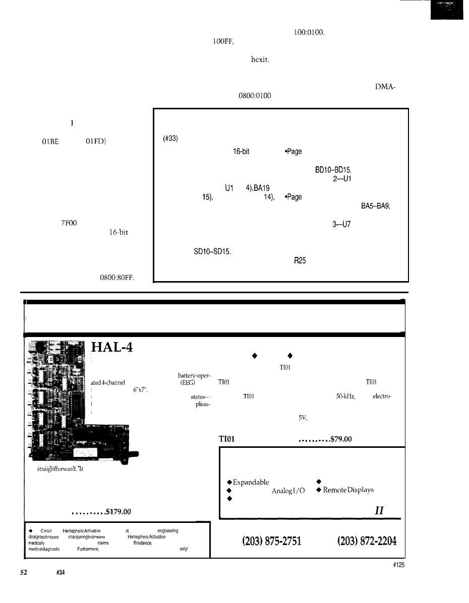
One reader reported (on the BBS)
that the diskette boot loader from
issue 3 1 didn’t work with the Award
BIOS
in his
‘486 system. I had tested
the code with an old ‘286 AT, a ‘386SX
laptop, and my ‘386 Model 80, but
there’s always one more system....
The problem seems to be that the
Award BIOS expects the last two bytes
of the boot sector to be 55AA rather
than the OOED used. It turns out that
a valid hard disk partition table (at
offsets
through
will be
followed by those marker bytes. Of
course, diskettes do not have hard disk
partition tables, so the marker bytes
are just there.
However, the boot loader has a
somewhat more serious problem.
Although the code looks like it can
handle files up to 64K bytes, it will fail
after reading
bytes. I forgot that
the diskette interface uses a
DMA controller that cannot transfer
data that crosses 64K byte physical
address boundaries.
The loader hit this problem when
it tries to load a sector at
The corresponding physical addresses
to
By starting the load at
are OFF00 through
and the
physical address 10100 the file can be
DMA hardware simply cannot handle
up to FFOO bytes before the address
the “carry” into the high-order
wraps. Because the binary files we are
The BIOS routine will return error 9:
using with the loader are limited to
Attempted DMA across 64K boundary.
that size, we’re in good shape.
The quick-and-dirty fix is to
change the load point from
Eventually we’ll build a
capable interface and 1’11 be sure to
Corrections
A number of mistakes crept into the Firmware Furnace schematics in the April issue
during editing. Please take note of the following:
*Page 46, Figure l-The
46, Figure l-On U5, signals
extension portion of the bus should
connected to pins 16-l 1 should be
have SD15 (pin 18) connected to the
labeled
bus bar with the rest of the data lines;
*Page 51, Figure
la pin 8 should
similarly, SA18 on (pin
be connected to ground.
on Ul (pin
BAEN on Ul (pin
51, Figure 2-U14 pins 12, 9, 7, 5,
and SD6 on U4 (pin 8) should all be
and 3 should be labeled
tied to the bus bars nearest the signal
respectively.
names.
*Page 52, Figure
and U8, pin 10
*Page 46, Figure l-On U5, signals
should be connected to ground and
connected to pins 4-9 should be
pin 20 should be connected to Vcc.
labeled
*Page 52, Figure 3-The label above
should read “Left Digit (MSD).”
We regret any problems these mistakes may cause our readers.
CIRCUIT CELLAR KITS
Sonar Ranging Experimenter’s Kit
EEG Biofeedback Brainwave Analyzer
Targeting Ranging Machine Vision
The Circuit Cellar
Ultrasonic Sonar Ranger is based on the
The HAL-4 kit is a complete
sonar ranging circuitry from the Polaroid SX-70 camera system. The
electroencephalograph
which
and the original SX-70 have similar performance but the
Sonar
measures a mere
HAL is sensitive enough
Ranger requires far less support circuitry and interface hardware.
to even distinguish different conscious
The
ranging kit consists of a Polaroid
300-V
between concentrated mental activity and
static transducer and ultrasonic ranging electronics board made by Texas
ant daydreaming. HAL gathers all relevent alpha,
Instruments. Sonar Ranger measures ranges of 1.2 inches to 35 feet, has a
beta, and theta brainwave
TTL output when operated on
and easily connects to a parallel
signals within the range of
printer port.
4-20 Hz and presents it in a
serial digitized format that
Sonar Ranger kit.
plus shipping
can be easily recorded or
analyzed.
HAL’s operation is
CHECK OUT THE NEW CIRCUIT CELLAR
samples ‘four channels of analog brainwave data 64
HOME CONTROL SYSTEM
times per second and transmits this digitized data serially to a PC at 4800
bps. There, using a Fast Fourier Transform to determine frequency,
amplitude, and phase components, the results are graphically displayed
in real time for each side of the brain.
HAL-4 kit
plus shipping
Network
Trainable IR Interface
Digital and
X-IO
Interface
Call and ask about the NCS
The
Cellar
Level detector presented as an
example of the
used
signals. This
Level detector
IS
not a
approved device, no medical
are made for
and it should not be used for
purposes.
safe use requires that HAL be battery operated
To order the products shown or to receive a catalog,
call:
or
fax:
Circuit Cellar Kits
l
4 Park Street
l
Suite 12
l
Vernon, CT 06066
Issue
May
1993
The Computer Applications Journal
cover this topic in more detail so we
can all get it right. Until then, remem-
ber that diskette I/O can’t cross 64K
byte physical memory boundaries and
you’ll be OK.
The downloadable files this
month include a revised boot loader
with the 55AA flag and a new program
load address. You don’t need to modify
Dunfield’s MON86 because it doesn’t
use DMA to load hex files through the
serial port.
I’d hoped to get to interrupt
hardware this month, but it deserves
more space than I have left. Next
month I’ll use the new 8254 timer to
explore interrupt response times and
then twiddle the PC’s sacred interrupt
structure so IRQ 0 no longer produces
INT 8.. and that takes some explain-
ing!
Ed Nisley is a Registered Professional
Engineer and a member of the Com-
puter Applications
engineer-
ing staff. He specializes in finding
innovative solutions to demanding
technical problems.
Ed
ISA EISA Theory and
Operation
is
available from
Annabooks Fax for $89.95 plus
shipping. It replaces his earlier AT
Bus Design book and goes into much
more detail on the EISA specs.
Annabooks is at 15010 Avenue of
Science
San Diego, CA 92128,
phones (800) 462-1042, (619) 673-
0870, or fax (619) 673-1432.
Jim Mischel’s Macro Magic with
Turbo Assembler (John Wiley
Sons, ISBN O-471-57815-0, $39.95)
suffers from a terminally cute title,
but will give you the dope on an
aspect of assembler programming
that isn’t explained elsewhere. He
even builds a useful language
entirely in macros; if you liked the
mini-interpreter I discussed in issue
30, you’ll love this. I haven’t gotten
all the way through the book, but it
looks good so far. Available from the
usual book sources; see the listing in
issue 3 1.
The 8254 timer and other parts are
readily available from the usual
sources, but Pure Unobtainium has
the bits and pieces as well as a
complete schematic for the Firm-
ware Development Board’s circuitry
so far. Pure Unobtainium is at 89
Burbank Road,
CT
2416, phone or fax (203)
Software for this article is avail-
able from the Circuit Cellar BBS
and on Software On Disk for this
issue. Please see the end of
in this issue for
downloading and ordering infor-
mation.
410 Very Useful
411 Moderately Useful
412 Not Useful
is the Schematic Capture for
anyone
needing to enter designs. Provides
multi-sheet,
user configurable partslist Electrical Rules Check report.
A n e w a u t o r o u t e r u s e s a n a d v a n c e d
ARFS PCB
strategy to achieve very high connection rates it’s fast!
copper layers, Design Rule Checker and MORE.
R4 SYSTEMS Inc.
451
DEMO
Package
West Hill, Ontario
Canada Ml E
(416) 898-0665
The Computer Applications Journal
Issue
May 1993

Squeeze
That Battery
‘Till It’s Dry
Jeff Bachiochi
enjoy week-
ends. It’s a chance
to catch up on those
little chores all
homeowners enjoy. I only wish my
money compounded interest as fast as
the number of slips added to the job jar
seem to. Nothing like a little work on
Saturday to keep your mind off of the
inevitable-the Sunday morning
newspaper. You probably don’t realize
just how scary the Sunday morning
paper can be. I’m not talking about the
skimpy daily edition, but the
multipound Sunday morning special.
Understand the world doesn’t hold
off its news stories until the weekend;
no, the extra bulk here is not news, it’s
advertising. Did I hear you say, “So
what?” Well, this may not cause
problems at your house, but at ours,
my wife, Beverly, goes over the ads
with the skill of Sherlock Holmes.
This isn’t a problem in itself, the
problem comes from a “Pavlovic”
response to the word SALE. I can’t tell
you how much money she saves us, or
how much these savings cost.
THE BALANCE
Whether it’s managing the home
budget or the latest project at the
office, acrobatics play an important
role. Each component’s effectiveness
must be in balance with the additional
parts count it brings, since they
become a factor of the component’s
“cost.” When a product must be
portable,
of its size and weight
is batteries. Squeezing every last
coulomb out of those batteries is
important. But, before you go bald
designing for efficiency, try to select
the right battery to start with.
CUTE AS A BUTTON
The first group of cells is named
after its recognizable shape. Small
“button” cells are used in watches,
calculators, hearing aids, singing
Christmas cards, and those irritating
little
noise makers. These
cells are constructed using various
materials which produce unique
voltage outputs: mercuric oxide
1.4
V), silver oxide
V), lithium
manganese dioxide (3 V), and zinc air
(1. l-l
V). Discharge curves for all
button cells are relatively flat over
most of their operating life. Although
their practical current drain rates are
in the microampere range, with typical
capacities in the milliamp-hour range.
Larger lithium cells are being made
with capacities up to 0.5 AH. These
larger cells are the size of a quarter and
are used mainly as battery backup
devices.
The second group of cells is the
most common. It consists of the
familiar cylinders that power our
flashlights, walkmans, and IR remote
controllers. The carbon zinc, zinc
chloride, and alkaline manganese
dioxide construction all produce 1.5
volts. Discharge curves are sloped over
the operating life of the cell, but the
current-drain ratings are much higher
than button cells. Current drains are in
the milliampere range with upper
capacities in the amp-hours.
The third group of cells is similar
in size to the second, because the cells
are produced to be a direct replace-
ment for them. Nickel-cadmium cells
generate 1.2 volts and are rechargeable.
can support higher current
drains A), but their capacities are
somewhat less than their carbon-based
Number of cells Cell voltage
Total voltage
5
1.5
7.5 volts
1.2
6.0 volts
6
1.5
9.0 volts
1.2
7.2 volts
Table
l--The use of series-wired
as
unregulated inputs for linear regulators results in five
not being enough for a minimum input of 6.5 V
However. the carbon zinc, zinc chloride, and alkaline
types suffice.
54
Issue
May 1993
The Computer Applications Journal
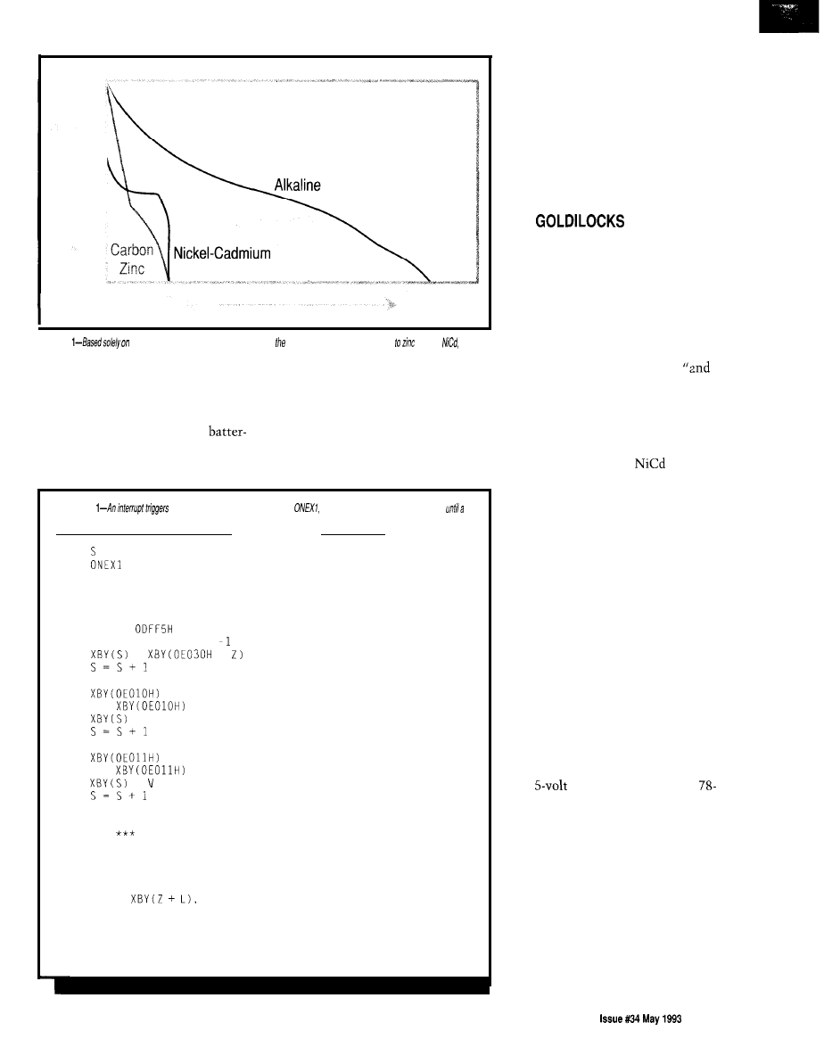
Figure
time, the alkaline batteries last longest when compared
chloride,
and
carbon zinc
batteries.
cousins. The capability of being
recharged many times offsets their
higher initial costs. And, like the
button cells, nickel-cadmium
ies have relatively flat discharge
curves.
The final group I’ll mention is the
sealed lead acid cell. Sister to the
automotive battery, the lead acid cell
typically produces 2.3 volts (open
circuit) and is packaged in groups of
three or six cells to produce 6 or
12
Listing
a storagesequence using
otherwise the program checks
key
is pressed.
10
= 8000H
20
60
30
G = GET
40
IF G = 0 THEN 30
50
GOT0 220
55
REM *** STORE
60
IF S >
THEN RET1
70
FOR Z = 9 TO 2 STEP
80
=
+
90
100
NEXT Z
110
= 0
120
V =
130
= v
140
150
PRINT V,
160
= 0
170
V =
180
=
190
200
PRINT V
210
RET1
215
REM
DISPLAY
220
CLEAR1
230
240
FOR Z = 8000H TO S-l STEP
250
FOR L = 0 TO 9
260
270
NEXT L
280
290
NEXT Z
300
GOT0 20
: REM
: REM
: REM
: REM
: REM
: REM LEAVE IF PAST END
: REM ALL TIME INFO
: REM STORE A BYTE FROM CLK
: REM
: REM
: REM
: REM
: REM
: REM
NVRAM START
JUMP ON INTERRUPT
OTHERWISE KEY PRESSED?
NO LOOK AGAIN
YES JUMP TO DISPLAY
ALL TIME INFO
CHANNEL 0 SET
READ IT
STORE IT
PRINT IT
NOW CHANNEL 1
: REM
: REM STOP INTERRUPTS
10 : REM EACH RECORD
: REM ALL BYTES
: REM PRINT
: REM
: REM
: REM
RETURN FROM INTERRUPT
NEW LINE FOR
NEXT RECORD
RESTART INTERRUPT
volts. The high discharge rates and
large capacities of these batteries don’t
occur without cost. Sealed lead acid
batteries are very bulky and are not
usually used in most portable equip-
ment, but rather they are applied as
backup power sources for emergency
lighting and uninterruptable power
supplies.
THE
SYNDROME
Goldilocks checked the stats.
“Button cells are too weak,” she
sighed, “and lead acid cells are just too
heavy,” she groaned.
“Take the carbon or NiCds,
they’re just right,” said Mama bear,
the clerk at the Bear’s Country Store.
“Okay. I’ll take the NiCds.”
Goldilocks paused, then added,
charge ‘em.”
To see the stats Goldilocks
referred to, take a look at Figure
1.
The
four curves indicate the relative
discharge curves for carbon zinc, zinc
chloride, alkaline, and
cells (the
ones you’re most likely to use). These
curves are given for a continuous duty
load. As a battery discharges, the
voltage across its known load goes
down, and so does the current through
the load over time. However, this is
not
the discharge curve a regulated
battery system would have. In a
regulated power supply the output
voltage will be fixed. A known load
will always draw a known current. As
the unregulated voltage drops, the
current draw will remain constant,
discharging the battery at a more
linear rate.
Effective battery life is a measure
of the duration a battery can sustain a
voltage high enough to maintain
proper regulation. If we are dealing
with
circuitry, the standard
series linear regulator typically needs a
2.0-volt drop to regulate the output
correctly. Multiple cells in series can
be used as unregulated inputs for
linear regulators. Table
1 shows how
the voltages from series-wired batter-
ies stack up.
Five cells isn’t enough for NiCds
[when using 6.5 V as the minimum
input voltage). Using six cells (a nice
even number] leaves a bit of head
room. It’s this head room that will
The Computer Applications Journal
5 5
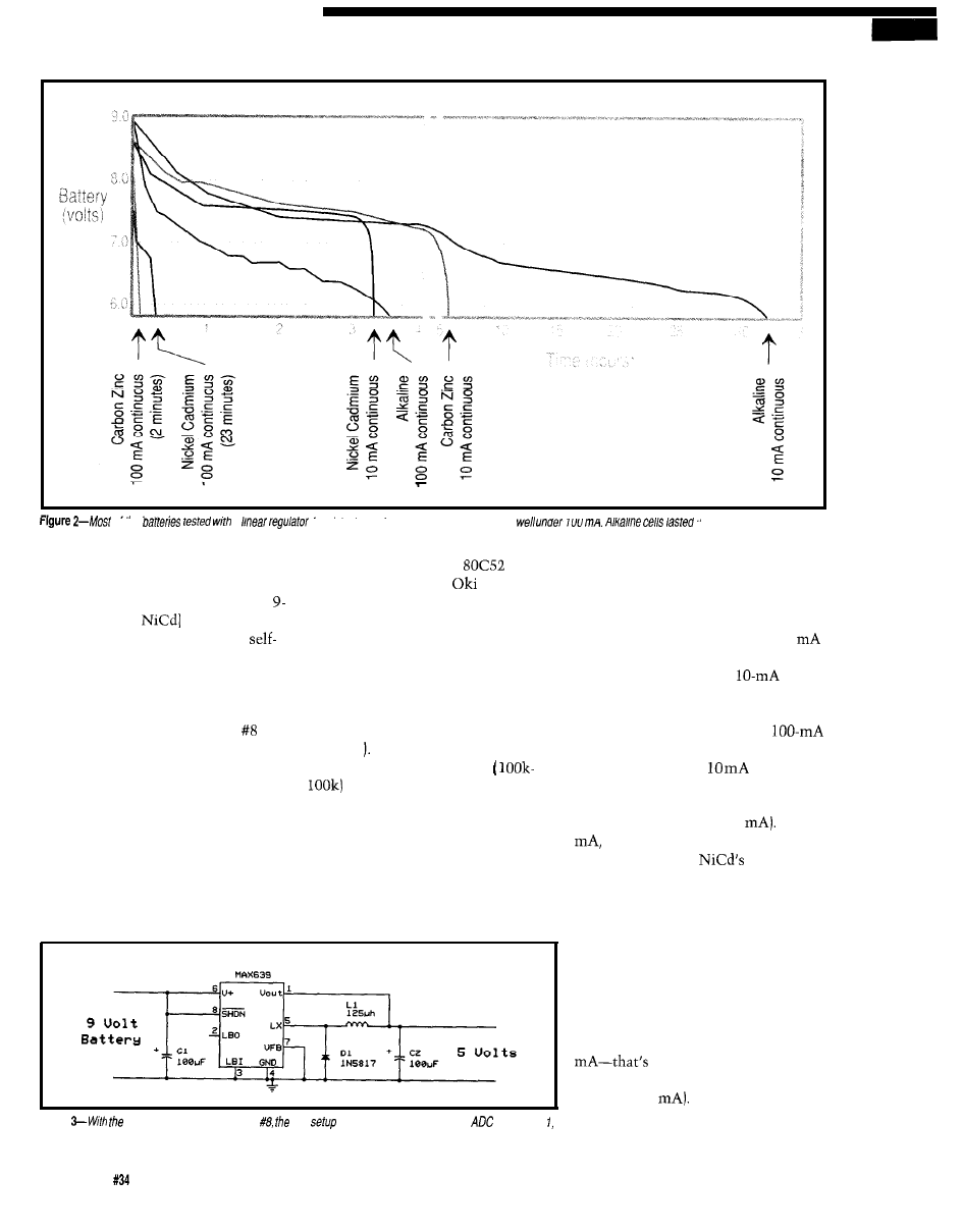
Of me
a
tared fhe best when current consumption was
cells maintained a higher constant voltage until suddenly giving up.
me longest, though other
determine effective battery life. (The
following experiments use 9-volt
batteries as their source supply. The
volt (7.2 for the
battery is the
easiest to work with since it is a
contained multicell device.)
COLLECTING REAL DATA
I dusted off some circuitry that I
designed back in 1989 for issue to
help make some observations on
battery life. The RTC52 and RTCIO
make great bench companions,
fulfilling many of my data collection
requirements. So, I hooked them up to
monitor the performance of several
different types of batteries. I wanted to
log the battery voltage and regulated
voltage over time to determine
effective battery life. A simple BASIC
were my measurement channels
program loaded into the
stored
during this experiment). The clock
chip is set up to provide time-based
a time stamp from the
clock/
interrupts (one minute apart) which
trigger the storage sequence using an
calendar along with the first two
0 N EX 1 BASIC statement (refer to
Listing 1
inputs from the A/D converter (which
A simple resistor divider
on the battery is used to divide
the battery voltage down for channel 1
since the ADC accepts a maximum
input of 5 volts. Channel 2 is read
directly as the regulated output for
comparison.
The effective battery life for
circuits using linear regulators is
produce a sustained current of 100
for more than a couple of minutes.
shown in Figure 2. These graphs were
However, under a lighter
load,
battery life is extended much longer
produced from the measurements
I
than the 10 times you might expect.
The alkaline cell can sustain a
took with my battery-loader and test
load over a period of hours, while
lowering the load to
extends its
jig. The carbon zinc version cannot
serviceable life to days. Nickel
cadmium gives up its complete charge
in less than 1 hour (at 100
At 10
its life is extended by a factor of
10. This shows the
ability to
supply power is independent of its
current drain (to a limit).
Figure
help of circuitry built for issue test
uses a voltage divider for the
on channel
while channel 2 is read directly as the regulated output.
5 6
Issue
May
1993
The Computer Applications Journal
There is an inefficiency at work
here. While the battery voltage is at its
highest levels, its power expenditure is
also highest (remember the current
through our load is constant due to the
linear regulator). For example, immedi-
ately after starting a test, the battery
voltage is 9 V and the current is 100
0.9 W out of the battery.
The load, on the other hand, uses 0.5
W (5 V x 100
Conversion effi-
ciency at this point is 55% (0.5 W/O.9
W). To be most efficient, a battery’s
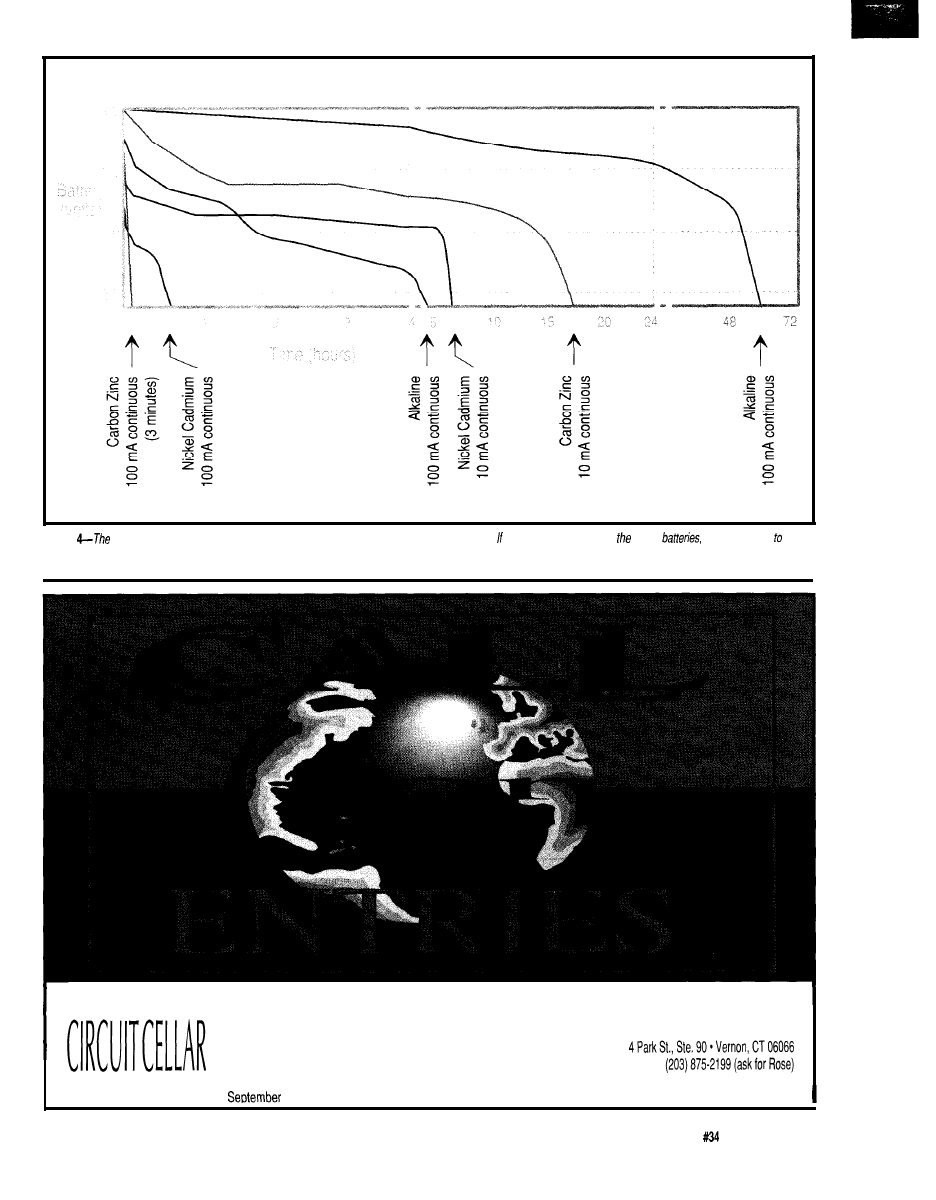
Figure
optimum use of batteries is with a switching regulator. Efficiencies can improve greatly. your next project involves use of
if would be wise
implement a switching regulator info your circuit for maximum performance.
An Official Entry Form must accompany all entries. To receive an Official Entry Form and a complete set of contest rules,
write or call:
Circuit Cellar Design Contest
DESIGN CONTEST
Fax: (203) 872-2204
All entries must be received bv
17, 1993. Prizes include $500 for first, $200 for second, $100 for third, and $50 honorable mentions.
The Computer Applications Journal
Issue
May 1993
5 7
output power should
equal the power in the
load throughout the
entire discharge cycle.
E FISH’N C
While the linear
regulator is simple and
inexpensive, unless you
have tight controls on
the input voltage and
drop as little across the
regulator as possible,
they are not very
efficient. A simple
switching regulator can
bestow efficiencies up to
or so they say.
Let’s find out if what
Linear regulator circuitry
Input Capacitor
$0.50
Regulator
$0.75
Output Capacitor
$0.50
Total
$1.75
Battery exchanges cost per 100 hours
load)
Carbon Zinc
($0.99) 17
$18.43
Alkaline
($3.49)
($11.19)
$10.47
$11.19
Battery exchanges & cost per 100 hours
load)
Carbon Zinc
($0.99)
N/A
N/A
Alkaline
($3.49) 28
$97.72
($11.19)
300
$11.19
Switching regulator circuitry
Input Capacitor
$0.50
Coil
$1.30
MAX639
$3.15
Output Capacitor
$1.50
Diode
$0.50
Total
$6.95
Battery exchanges cost per 100 hours
load)
Carbon Zinc
($0.99) 6
$5.94
Alkaline
($3.49)
$6.98
($11.19)
$11.19
Battery exchanges cost per 100 hours
load)
Carbon Zinc
($0.99)
N/A
Alkaline
($3.49) 20
$69.80
($11.19) 66
$11.19
Table
kind of
and regulator circuit you use depends on
expected load and the price you’re
pay. prices
are for 100 quantity.
they say is true. Maxim, Linear
Technology, and National Semicon-
ductor (among others) manufacture
switching regulators. I chose to use a
Maxim MAX639 because it is inexpen-
sive and does not require any specially
wound toroidal transformers. Only
three external components are used
(see Figure 3).
The MAX639 is a DC-DC
down converter. An internal oscillator
drives a FET switch which applies the
battery voltage across the coil and
capacitor. When the FET opens, the
coil’s stored magnetic field collapses
transferring its energy into the capaci-
tor. The built-up charge on the
capacitor is monitored closely by a
comparator inside the MAX639. The
comparator’s output is used to keep
the oscillator at the ideal frequency
and duty cycle necessary to maintain
the desired charge on the output
capacitor, while keeping the peak
currents constant throughout the
battery’s discharge cycle, thus maxi-
mizing useful battery life.
V25 POWER COMES TO EMBEDDED CONTROL!
Micromint’s RTCV25 is the perfect marriage of an
processor, programming convenience, and control
Forget
the need for cross-assemblers and cross-compilers; your favorite high-level language for the PC and a “locate” facility are all you
need. The RTCV25 enhances the
power with parallel
A/D conversion;
and RS-485 serial ports; up to 384K of
RAM and EPROM; a battery-backed clock/calendar; 128 byte EEPROM, ROM monitor, and the RTC stacking bus. Ease of code
development combined with its small size and low power consumption make the RTCV25 ideal for all embedded control applica-
tions. And of course the RTCV25 is compatible with Micromint’s full line of RTC peripheral boards and products.
Features:
l
8 MHz CMOS NEC
V25 processor
l
Up to 384K of RAM
and EPROM
l
Two serial ports
l
Battery-backed
calendar
l
128 byte EEPROM
l
40 parallel lines
l
&channel, (or
bit ADC
l
RTC stacking bus
l
Small 3.5” x 5” size
l
only operation
(150mA max.)
l
Full featured ROM monitor
l
operating system
100
OEM configuration
$270
4
Park St.
l
Vernon, CT 06066
c a l l l - 8 0 0 - 6 3 5 - 3 3 5 5
871-6170
l
Fax:
872-2204
5 8
Issue
May 1993
The Computer Applications Journal
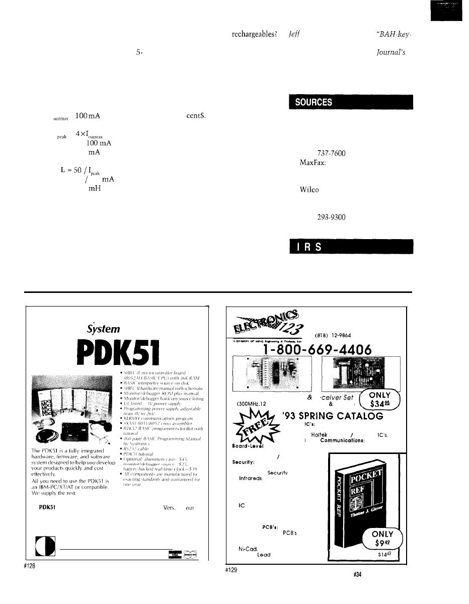
The MAX639 regulates to 5 volts
unless you add two resistors in the
feedback circuit. But since I want a
volt output, I left them out. Compo-
nent values for the other components
in the regulator circuit are calculated
with respect to the maximum operat-
ing current as shown below:
I
=
I
=
=4x
= 400
= 50 400
=
125
The battery load and measure-
ment tests are now rerun using the
same prior loads. See Figure 4 for the
results of this test.
The costs associated with using
this component are given in Table 2.
You be the judge. Questions you may
ask yourself are: How often can your
customer stand changing batteries? Do
they mind dealing with
You must determine to what extent
you will go in order to provide your
customer the best possible product.
Also, if you consider our planet’s finite
resources-both the raw materials
needed to produce batteries and the
cost of safe disposal or recycling of
discharged cells-rechargeable batter-
ies make
ONE FINAL CAVEAT
I made no attempt in this experi-
ment to cover the effects of tempera-
ture or intermittent duty on battery
life. All tests were made on 9-V cells
at room temperature. As an alternative
to the 9-volt batteries’ small cell
energy density, you may choose to use
multiple
1.5-V
cylindrical cells in
your next portable project. If so, you
can expect about 30% more from
AAA cells, 100% more from AA
cells, 500% more from C cells, and
1200% more from D cells. Your
mileage may vary slightly depending
on load size and battery type. Happy
motoring.
q
Bachiochi (pronounced
AH-key”) is an electrical engineer on
the Computer Applications
engineering
staff.
His background
includes product design and
manufacturing.
MAX639
Maxim Integrated Products, Inc.
120 San Gabriel Dr.
Sunnyvale, CA 94086
(408)
(408) 749-6801
Ferrite Bobbin Coils
Corp.
645 1 Saguard Ct.
Indianapolis, IN 46268
(317)
Fax: (3 17) 293-9462
413 Very Useful
414 Moderately Useful
415 Not Useful
The $595 Solution
to 8051
Development
PLUS
includes everything in the PDK51 plus
3 of
popular BXC51 805118052 BASIC compiler-$800.
Call Now! 508-369-9556 or FAX 508-369-9549
Binary Technology, Inc.
P.O. Box 541
l
Carlisle, MA 01741
17921 Rowland Street
City of Industry, CA 91748
Technical Support:
V I S A
9
MASTERCARD
and DISCOVER
RC-99
RF Transmitter Re
bit address or 6 address 4 data.)
DRAM memory.
Encoder Decoder
Radio
Items:
Motorola Spirit Radios.
Digital Voice Modules.
RF Transmitters Receivers.
Auto Alarms and Accessories.
X-10 Home
Accessories
Tools:
Soldering Irons.
EPROM Erasers.
Fluke DMM.
Testers.
Industrial PC
EPROM Programmers.
Ultrasonic Measuring Device
Prototyping
Full line of Syntax
Batteries:
Alkaline
Sealed
Acid.
Button Cell.
Pocket PC Ref. for
The Computer Applications Journal
Issue
May
1993
59
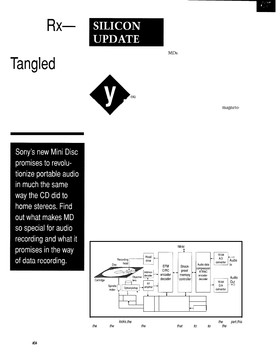
Audio
Skippy CDs?
Tapes? Call
an MD...
Tom
Cantrell
may be
‘wondering why a
Silicon Valley guy
like me is writing an
article about Sony’s new Mini Disc
(“MD”) digital audio technology
(Photo
1).
Certainly, I have no pretension to
being an A/V expert. In fact, despite
my immersion in MIPS, BOPS, and
FLOPS, I’m quite the Luddite when it
comes to the latest and greatest
consumer gadgets. I’m one of the
unwashed masses who can’t even
figure out how to make their VCR
work.
Justification for an MD article
goes beyond its musical merits.
Rather, I’d like to highlight how this
marvelous device exploits advanced
of the CD and furthermore, the raw
data-encoding and error-correction
format is the same for both MD and
CD. Besides exploiting proven read
concepts, format compatibility means
that prerecorded [i.e., “playback-only”)
are easily added to existing CD
production lines. In both formats, pits
encoding the data are formed in an
aluminum reflective layer laminated
to a plastic disc.
Otherwise, the MD (Figure
1) is
quite different from the CD and it is
these differences that define MD’s
compelling advantages.
Clearly, the knockout punch is
MD’s recordability based on
optical (MO) technology. With durabil-
ity and random access in MD’s favor,
it seems reasonable to expect it will
ultimately replace tape in most
applications.
With only about one quarter of the
surface area of a CD, how does MD
manage to store the same amount (74
minutes) of audio? The secret is an
advanced data compression scheme
that packs more music into each bit.
CDs are known to skip when
subjected to the jarring encountered in
portable or automotive applications.
The MD includes 4 megabits of
DRAM configured as a shock-proof
memory which buffers the audio while
technology to work its magic. As
the head gets back on track.
you’ll see, advanced silicon-what this
column is all about-plays a very big
MO BASICS
role.
The MO disc combines “M” and
For playback, the MD uses an
“0” layers as shown in Figure 2.
optical read mechanism similar to that
Grooves that cover the entire disc
DRAM
Feed motor
Servo
System
Display
control
Key
Figure l--Just from ifs
Mini Disc player closely resembles a typical CD Disc player. For
most
is extent of similarities befween two. One major feature
is going be hard resist is capability
to erase and record data and music.
6 0
Issue
May
1993
The Computer Applications Journal
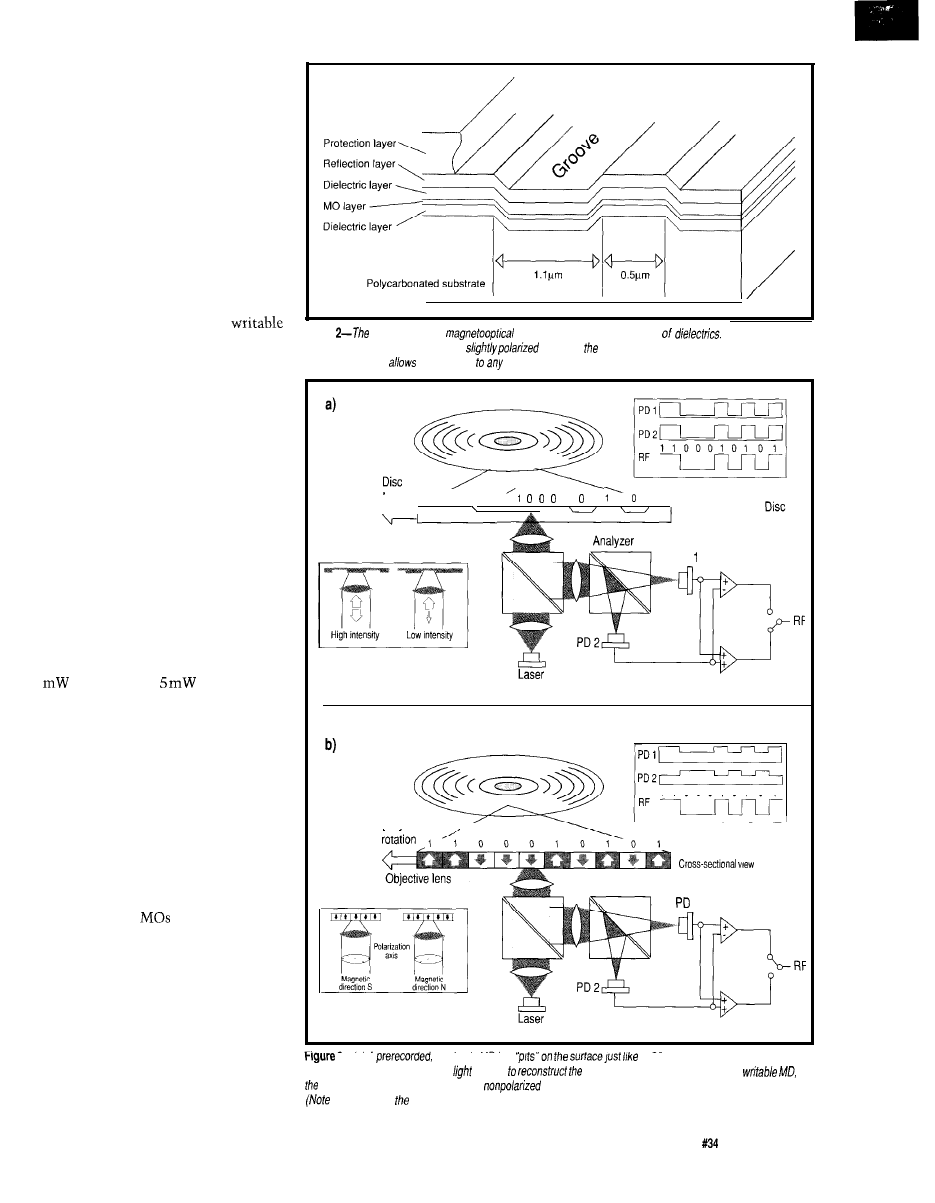
cleverly encode address information
(supporting random access) by “mean-
dering” slightly. The difference in
reflection depends on whether adjacent
grooves have a small or large gap.
For reading, MO technology relies
on a dual-function pickup that com-
bines a laser/lens arrangement with a
beam splitter and two photodetectors.
When reading a read-only disc, the MD
simply checks (just like a CD) for the
total amount of reflected light by
summing the two photodetector
outputs (Figure 3a).
However, when reading a
disc, a different technique is used in
which the beam splitter funnels light
to one photodetector or another
depending on slight variation in
polarization (Figure 3b). In this case,
the difference between the two
photodetector outputs determines
whether a
1
or 0 is read.
The MO scheme relies on a
phenomenon known as the Kerr effect,
in which the polarization of the
reflected light varies slightly depend-
ing on the orientation of a magnetic
field.
MO writing is accomplished by
polarizing the magnetic layer. The MD
uses a “magnetic-field modulation
overwrite” technique (Figure 4) in
which laser power is boosted (from 0.5
for reading to
for writing).
The laser heats the MO layer to a
temperature (about 180°C) sufficient to
dissipate any previous magnetization.
At the same time, a magnetic head on
the opposite side of the disc applies the
newly desired magnetic field to the
disc. The revolving disc cools and the
applied field is retained.
Note that, in principle, MO
writing could also be accomplished by
modulating the laser instead of the
magnetic field. Indeed, that approach
is used on data
to allow higher
capacity and speed since a laser can be
switched much faster than the 100
nanoseconds or so required to achieve
flux reversal with an inexpensive
magnetic head.
However, laser modulation comes
at a price. First, it doesn’t support
overwrite. Instead, either two lasers
are required (one for erasing and one
for recording, just like a tape) or a
Figure
Mini Disc uses a
layer sandwiched between a pair
When reading a
recorded signal, the reflected light is
based on
polarity of the recorded magnetic field (the Kerr
effect). The groove
quick access
portion of the disc even if nothing has been recorded
yet.
rotation
1
,
1
Objective lens
Premastered Mini
Cross-sectional view
PD
1 1 0 0 0 1 0 1 0 1
Disc
Recordable Mini Disc
Analyzer
1
‘Z--(a)
A
read-only MU has
a CD and
IS
read the same way as a
CD. The total amount of reflected
is used
recorded signal. (b) When reading a
difference between the polarized and
reflected light is taken and used to decode ones and zeros
the position of “RF” switch in both cases.)
The Computer Applications Journal
Issue
May 1993
61
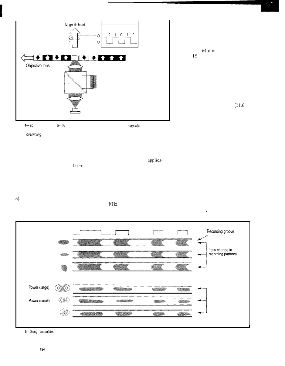
Disc
Writing Signal
rotation
New
Old
Recordable Mini Disc
Cross sectional view
Laser
Figure
write to an MD, a
laser heats up the medium from below while a
write bead records
ones and zeros from above. When the medium cools, the magnetic polarity is fixed. Rerecording is done in a sing/e
pass by
the previous information, eliminating the need for an erase head or a separate erase pass.
single head must do double duty to
laser is only used to heat the material,
erase and then record, complicating
not shape the recorded pattern.
the design of the head assembly and
The point is, given the acceptable
spindle servos.
density and speed for audio
Also, the consistency of a
tions, the MD’s lower cost, lower
modulated pattern varies significantly
power, and more rugged magnetic-
with power, causing a problem for
field modulation scheme makes good
battery-operated recorders. By contrast,
sense.
magnetic-field modulation is twice as
tolerant of power fluctuations [Figure
AUDIO TRICKERY
Like a CD, the MD digitizes data
A final advantage of magnetic-
at 44.1
Given 16-bit resolution
field modulation is resistance to tilt
and two channels, that translates into
during recording/playback since the
a
digital data transfer rate of about 180
it deems inaudible.
The ATRAC scheme compresses
blocks comprising 5 12 samples
ms) using a modified discrete cosine
transform (MDCT). This transform,
similar to that used in MPEG and
JPEG video compression standards,
converts the time domain source into
ordered frequency subcomponents
which are amenable to further crunch-
ing. Special filtering and signal
processing is applied to counteract any
vagaries, such as “pre-echo,” associ-
ated with the MDCT algorithm.
In particular, relying on a
“psychoacoustic” model of human
hearing, the various frequency values
can be quantized with differing degrees
of accuracy that closely reflect the
ear’s nonlinear response. Indeed, as
shown in Figure 6, the ATRAC
scheme will simply throw away source
Kbytes per second (i.e., 44.1 x 2
channels
x
2 bytes/channel) or about
10 megabytes per minute. With similar
recording density but much smaller
surface area, and all else being equal,
the MD’s tiny
disc would hold
less than minutes of audio.
Of course, the solution is data
compression, and Sony has come up
with the Adaptive Transform Acoustic
Coding (ATRAC) scheme that does
just that. Achieving up to 5: 1 compres-
sion turns 15 minutes of bits into 74
minutes [the same as a CD) of music.
Laser Beam Shape
Recording signals
Power (large)
Power (small)
Beam deformation
Magnetic field modulation system used in MD system
Overwrite system
Prominent change in
recording patterns
Beam deformatron
General laser modulation system
Figure
a
laser to accomplish magnetooptical writing is possible, however it is more costly to manufacture and the pattern recorded varies significantly with
power and misaligned recording medium.
62
Issue
May 1993
The Computer Applications Journal
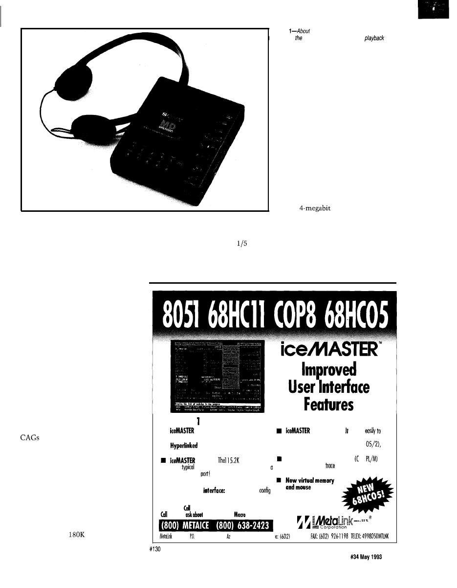
Sony faced a problem that’s
arguably emotional, but still pivotal:
convincing the recording artists that
ATRAC wouldn’t compromise their
artistic vision It wouldn’t do to have
Michael Jackson end up sounding like
one of the Chipmunks. In a classic
example of “show-me marketing,”
Sony toured the recording studios for
side-by-side sound-off challenge
between MD and CD.
ATRAC isn’t “perfect” in the
sense that judges could often detect an
audible difference between MD and
CD. However, they couldn’t effec-
tively describe the difference, and
most important, as often as not said
MD sounded better than CD.
I’m sure the lossy aspects of
ATRAC will serve as cannon fodder
for endless debate about whether MD
“sounds as good” as the uncompressed
CD. After all, some audio gurus
(known affectionately in the trade as
or Consumate Audio Geeks)
still argue that nothing matches the
good old LP and tube amp combo. All I
can say is, MD sounds just fine to me.
MUSICAL MEMORY
There is another big advantage
associated with data compression.
Remember that, because the data
density and linear velocity are similar,
the data transfer rate for MD and CD
is the same (the
bytes/second
demanded by the analog converters).
However, since MD’s ATRAC system
only calls for a fraction (e.g.,
assuming a 5: 1 compression ratio) of
that, the data transfer rate required of
the disc is correspondingly reduced.
Photo
the size of first-generation portable CD
players, portable MD unit allows both
and
recording in a compact package. A l-megabit memory
chip built into the playback section eliminates skipping
due to shocks or bumps.
With the disc transfer rate faster
than required, the MD can read ahead
and store yet-to-be-played music in an
on-board DRAM buffer. This is the
foundation of the “shock-proof
memory” which overcomes the
skipping associated, most notably in
cars, with CDs.
As shown in Figure 7, the MD
responds to a shock by drawing down
the buffer until the the head stabilizes
at which point the buffer is refilled.
With a
DRAM, the MD can
tolerate about 10 seconds of trouble,
enough to deal with even the worst
potholes.
PIRATES BEWARE
The MD isn’t the first recordable
digital audio technology. That honor
Rental And O-Day Trials Available
n
delivers productivity: easy
to learn,
easy to use and fost!
is convenient!
connects
your
PC, requires no disassembly, nor does it take up any
.
On-line help
guides you through the
exponsion slots. It works on any PC (DOS or
emulation process.
Micro Channel or EISA. Even laptops!
is FAST!
boud serial link
Supports source level debug
ond
and
keeps
download times to under 3 seconds using
source level trace. 4K
buffer with odvonced
standard COMM
searching and filtering copobilities.
n Broad support of derivative devices.
n Flexible user
you can completely
ure the windows for size, content, location and color.
todoyfor
FREEDEMODISK!
taday to
FREE 8051
Assembler!
Corporation Box
1329
Chandler,
85244-1329 Phon
The Computer
support.
9260797
Applications Journal
I s s u e
63
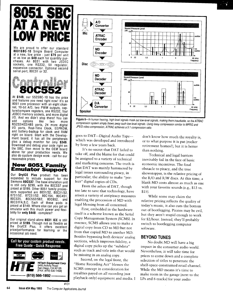
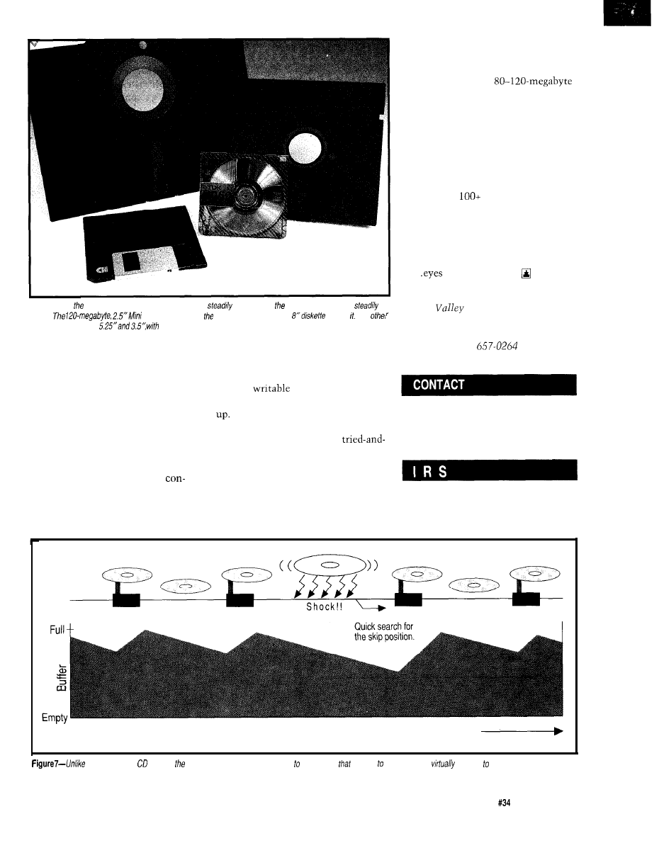
Silicon
for more than ten years
Photo 2-Over
years, fhe size of recording media has
shrunk while storage capacity has
grown.
Disc is dwarfed by much older, l-megabyte
behind The
popular disk sizes are
typical storage capacities of 1.2 and 1.44 megabytes, respectively.
example I’ve heard of is USL [now
Novell/Unix], which ships 93 dis-
kettes. Furthermore, since even
pedestrian PCs sport
hard disks, the idea of backing up to
floppy is more of a joke than it ever
was.
Wouldn’t it be nice if every PC
had an MD rather than the incompat-
ible gaggle of floppies and tapes that
currently litter the landscape? No
software package would require more
than a single
megabyte disc and
one or two blank discs would handily
back up all but the largest systems.
Whether it becomes the solution
for better sounds or the prescription
for bloated data, keep your eyes
(er..
and ears) on MD.
Tom Cantrell has been an engineer in
cassettes, Sony carefully states that
MD is designed to complement, rather
than replace, the CD. Frankly, their
justifications sound rather SWAT-like
(Sell What’s Available Today) to me. I
say the handwriting is on the wall and
it says “MD Rules.”
It doesn’t take a rocket scientist to
predict that MD also has great poten-
tial as a mass-storage device for
computers. Fueled by massive
devices. Even at high introductory
prices ($700 drive, $13 diskette), it’s
already quite competitive with
existing
technologies and,
needless to say, prices won’t be going
Also, the MD arrives just in the
nick of time as computing’s
true backup/interchange device-the
floppy disk-rapidly runs out of gas.
The problem is that software size
working on chip, board, and system
design and marketing. He can be
reached at (510)
or by fax at
(510) 657-5441.
Sony Corporation of America
1 Sony Drive
Park Ridge, NJ 07656-8003
(201) 930-1000
sumer volume, it’s likely that MD gear
continues to balloon with the most
416
Very Useful
and media will have a significant price
popular packages consuming half a
417
Moderately Useful
advantage over traditional “computer”
dozen (or more) disks. The worst
418
Not Useful
Time
today’s portable players, MD has an on-board DRAM buffer store music
is going play, making if
immune any type of shocks or
bumps usually encountered in portable applications.
The Computer Applications Journal
Issue
May 1993
6 5
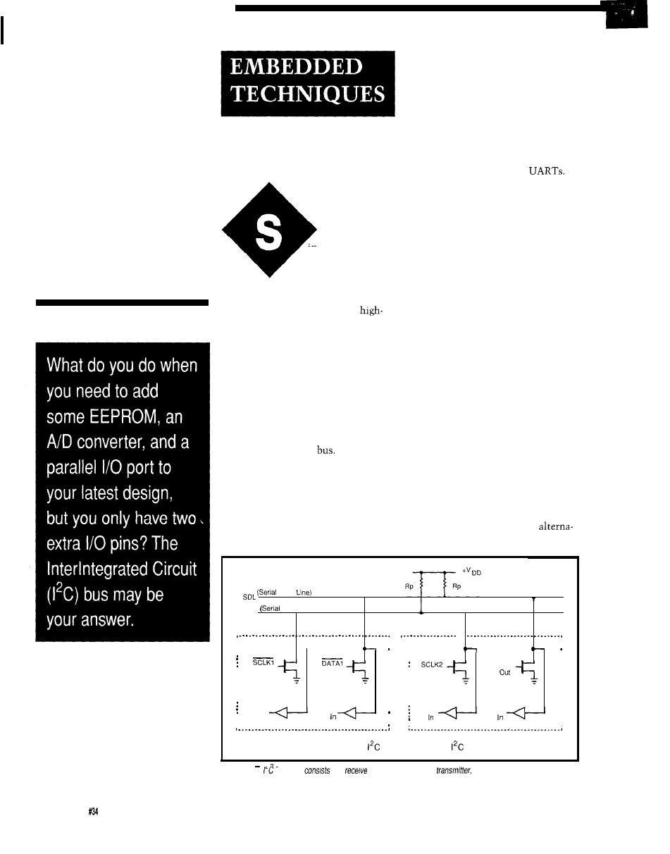
Interchip
Traffic
John Dybowski
erial methods of
interconnecting
peripheral functions
and microcontrollers are
popular. Although serial buses don’t
have the throughput of a parallel
interface, they work well when
speed data transfer is not a require-
ment. Often, the reduction in inter-
connecting wires and the need for
fewer pins offsets the slower speeds
inherent in this strategy. Frequently,
speed is not even an issue. Addition-
ally, this approach is attractive, and
perhaps the only choice, when work-
ing with several different single-chip
controllers that do not possess a
standard parallel data
Maybe the first thing you would
consider when selecting a serial
interface is whether a synchronous or
an asynchronous technique is the most
appropriate. The choice, as usual, is
based on the strengths and limitations
system constraints, and the nature of
the communications traffic. Many
times, the overall personality of the
system ultimately imposes what is an
acceptable communications solution.
For point-to-point communica-
tions between processors, you could
employ standard asynchronous
communications techniques using
either hardware or software
The asynchronous method is not
without problems since, to maintain
order in the communications flow,
some form of protocol is required in all
but the most trivial applications. The
protocol is needed to prevent data loss,
to synchronize fast and slow proces-
sors, and to handle periods of real-time
processing where a processor may have
to drop off-line to perform some more
critical operation. “Multidropping” is
an available option that allows
hanging multiple devices on the serial
cable but usually requires the designa-
tion of a master to moderate traffic.
You would most likely have to
resort to designing your own protocol
since this type of low-level communi-
cations would certainly have specific
needs. Remember, the crafting of a
communications protocol usually
amounts to no mean feat. In spite of
these problems, designing a custom
protocol may not be a bad way to go
for some applications. However, other
options exist that may be more
conducive to the task at hand and it
would be wise to consider the
of the mechanisms involved, the
tives before moving ahead.
Pull-up
Resistors
Data
SGL
Clock Line)
DATA2
o u t
o u t
o u t
SCLK
DATA
DATA
In
S C L K
Connection of
bus devices to the
bus
Figure l--The
interface
of a
buffer, an open-drain
and some external pull-up
resistors.
66
Issue May 1993
The Computer Applications Journal
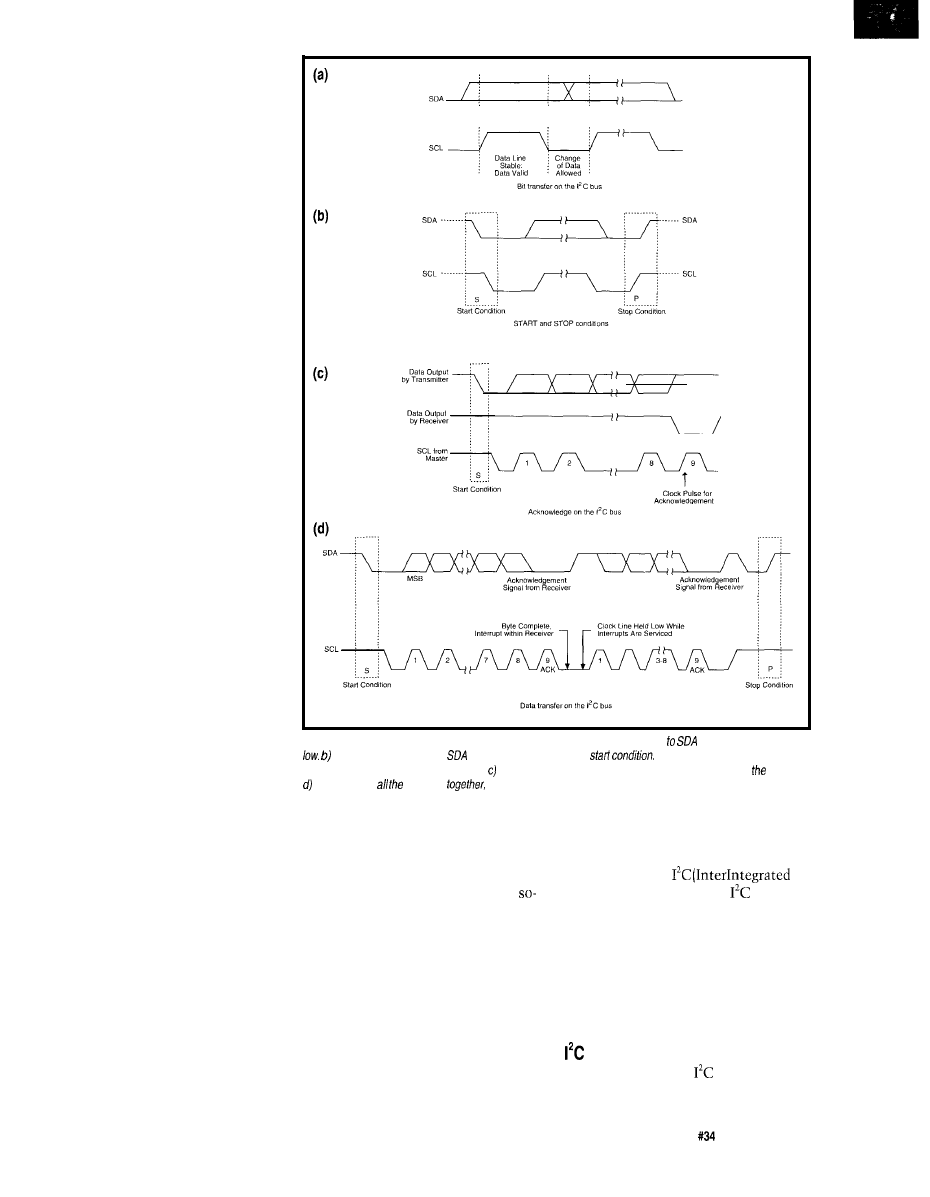
Synchronous communications
schemes exist where the data transfer
is performed under control of clock
pulses generated by a master control-
ler. The clock pulses signal when data
bits are valid for both the sending and
receiving devices. Clock-synchronized
data is a good thing (especially when
the clocking is done in software), since
the limiting factor is the maximum
clock rate. In most cases, the mini-
mum clock frequency can go all the
way down to DC. Synchronizing data
transfer to a clock signal means that
the controlling processor can go away
and suspend communications while it
attends to interrupts or to handle other
timely events. The ability of a master
clock to control communications
alleviates the rigors of asynchronous
modes where both the transmitter and
receiver must endure strict timing
constraints or face the prospect of
losing synchronization-and data.
The Motorola SPI (serial periph-
eral interface) is an example of a
synchronous, clocked-data-transfer
interface. Although it is a step in the
right direction, SPI is primarily
intended for point-to-point connec-
tions between a processor and a single
peripheral. A multitude of options are
available, presumably to allow greater
flexibility in the types of devices that
can be accommodated. In practical
terms, all of the options ultimately
make SPI sort of a nonprotocol.
Because of the lack of concrete
application guidelines, SPI offers little
hope for any kind of standardized
communications discipline, and
shouldn’t be applied beyond its
intended purpose.
Another clocked scheme is
National Semiconductor’s Microwire
that allows connecting multiple
peripherals to a single host controller,
but it suffers from a selection scheme
that requires individual chip selects for
each device on the bus. I’ve used
Microwire for connecting selected
peripherals to a controller. Microwire
is useful when you come up short on
controller pins or when the peripheral
must be located off-board and you
want to keep the interconnecting
wires to a minimum. The fact that a
lot of excellent parts are available that
Figure 2-a) During a bif transfer, SDA must be stable when SCL is high. Changes
are made while SCL is
A high-to-low fransifion of
while SCL is high signals a
A low-to-high fransifion of SDA
while SCL is high signals a stop condition. Every byte sent is followed by an acknowledge bit sent by receiver.
When you put elements
you have useful communication between components.
use the Microwire interface helps
make it more palatable if your com-
munications requirements aren’t too
stringent. Frankly, I find the need for
multiple discrete chip selects on a
called serial bus ridiculous. The
additional chip select wires tend to add
up rather quickly. So, I have never
given Microwire serious consideration
as a means of chaining together
multiple chips, due to its serious
limitations.
So, if you could eliminate the need
to contrive a communications proto-
col, keep the pin count low regardless
of the amount of chips on the bus, and
have access to a multitude of useful
peripheral functions, you’d really be on
to something. These desires are
embodied in the
Circuit) bus. Additionally,
provides
a simple, but effective, arbitration
scheme required for resolving
multimaster conflicts. This makes the
bus not only suitable for hooking up
peripherals, but also allows it to be
applied for processor-to-processor
communications.
WIRES
Electrically, the
interface
consists of two wires that are pulled
The Computer Applications Journal
Issue
May 1993
67
up to a positive supply voltage with
resistors. These wires are used to carry
the clock
and data (SDA) signals
and connect to bidirectional pins on
the various bus members. Since
collector (or open-drain) output stages
are used, the lines can be simulta-
neously asserted by any of the devices
on the bus without causing electrical
problems. The bus architecture is
flexible and can be used for stringing
together a number of peripheral chips
that operate under control of a single
master controller. Multiple masters
can also reside on the bus permitting
direct communications between
controllers, or perhaps via shared
peripheral chips. Standard peripherals
can transfer data at the rate of 100
kbps. The newer
components boost
the maximum data rate to 400 kbps.
Now it may appear that two wires,
a couple of resistors, and a bunch of
open-drain transceivers may offer little
potential towards the end of orches-
trating any kind of truly flexible
interface. Nothing could be further
from the truth. In fact, these
straints turn out to be the test of an
engineer’s
With these meager
resource?, some clear thinking, and
careful
you’ll see what can
be
Figure 1 shows the
interconnection scheme of the
bus.
The procedure of
communica-
tions defines unique start and stop
conditions, as well as a simple ac-
knowledgment procedure for ensuring
data validity. Before proceeding, let me
lay down some fundamental
tenets.
*The data on SDA must be stable
during the high period of SCL.
high-to-low transition of SDA
while SCL is high signals a
start condition.
*A low-to-high transition of SDA
while SCL is high signals a
stop condition.
*Data is transferred in
bytes, MSB first.
*The bus is considered busy
following the start condition.
*The bus is considered free a
certain time after the stop
condition.
*Every byte must be followed by
an acknowledgment bit.
The bit transfer and start and stop
conditions are depicted pictorially in
Figure 2. Note the relationship
between SCL and SDA. Also shown in
this figure is the progression of a
wide transfer that demonstrates how
the acknowledge bits are inserted by
the receiving device.
In practice, SCL is used for a
number of practical uses other than
just clocking data around the bus. The
clock can be used to empower receiv-
ers to cope with high-speed data
transfers on either a bit or a byte basis.
At the bit level, the
transfer can be
slowed down when the receiver holds
down SCL, effectively extending the
clock low period. A device may want
to cause the transmitter to wait in
order to process received data or to
perform some real-time processing.
This hold condition can be invoked by
pulling SCL low. This forces the
Everybody’s using
.
How do
get started?
IT’S
HERE! ACOMPLETE DSP DEVELOPMENT
BASED ON THE POWERFUL AND EASY TO PROGRAM
ADSP-2111 DSP CONTROL RESOURCES PC-21 11 NOW MAKES IT
EASIER THAT EVER TO BRING SPEECH TO YOUR PRODUCTS
COMPLETE HARDWARE The PC-21 11
a 12 MHz 2111 DSP,
Program RAM,
Data RAM,
and Speaker
I I .
Port.
also be used outside the PC with only a
power
,
COMPLETE SOFTWARE Included software allows
lo
An
framework and running speech
and
\
speech
code are also Included. The ADSP-2111
can
be
the card.
A COMPLETE SOLUTION In short, the PC-21
you
everything you need to get an
on your
DSP
If you
don’t know where to
Control Resources can quote on
or
custom hardware for your
write today for
information!
Resources
19042 San Jose Ave.
S,
0. Box 8694. Rowland
CA 91748
(818) 912-5722 (VOICE) (818)
(FAX)
Rugged Operator
For Industrial
Applications
$235
(7-24)
l
Inexpensive batteries supply power
for
months. Can also be externally powered.
l
FREE!
Custom labeling of logo and top keys
make this a part of your product.
l
Easy-to-read 4x20 display.
I
l
Handheld or panel-mount.
*Tactile
or
keypad.
l
Programmable
for status
indicators and operator alert.
l
Easy configuration lets you program
every key with up to 255 characters.
l
RS-232. RS-422 or RS-423 interface.
l
Optional bar-code wand interface.
68
Issue
May 1993
The Computer Applications Journal
master into a wait state until the bus
is freed by the release of SCL to a high
state. The clock is also used during
arbitration procedures to synchronize
the clocks of all transmitters in order
to accomplish arbitration for bus
control via SDA.
*The minimum output sink
current is 3
0.4 V
*The maximum capacitive
loading for each bus line is 400
ELECTRIC WIRES
allows connecting devices
with various input characteristics to
the bus. These can be broadly defined
as devices with fixed input levels and
devices with input levels that are
referenced to
input levels are
defined in such a way that both types
of inputs are accommodated. The
general
DC electrical characteris-
tics are specified thus:
*The low-level noise margin is
0.1
high-level noise margin is
0.2
The minimum sink capabilities
for output stages are specified as 3
and govern the minimum values for
pull-up resistors. The defined low-level
noise margin sets the maximum
values for the series protection
resistors. Bus capacitance is the total
capacitance seen by the device pins
and is composed of the wire capaci-
tance and the capacitance of the
connections and pins. The overall
capacitance limits the maximum value
of the pull-up resistors so that the
signal can make transitions within the
specified rise time. Refer to Figure 3
for an explanation of the DC and AC
parameters for SDA and SCL.
resistors of up to 300
BUILT-IN ADDRESSING
ohms can be used for protec-
Before proceeding, perhaps a brief
tion against high voltage
explanation of some basic terms
spikes on SDA and SCL.
pertinent to the
bus would be in
order. A bus master, as the name
implies, controls the transfer of data
on the bus and therefore controls every
slave. This is established by control of
the SCL line. (This is not to imply that
slave devices are excluded from
asserting SCL, but that they do so only
for purposes of synchronization.) The
operations the master can perform
include both reading from and writing
to the slave devices. It follows that the
master as well as the slaves can
function as both receivers and trans-
mitters.
All communications on the
bus are carried out over two wires.
These wires carry not only the data to
and from the peripherals, but they also
convey the address information used
to select the
prior to an actual data
transfer. Following the start condition,
a 7-bit slave address is usually sent.
Recall, that transfers over the
bus
occur in
chunks. The eighth bit,
contained in the address byte, is the
direction bit and signifies the direction
the subsequent transfer will take. A 0
indicates a write to the slave and a
1
Does your big-company marketing
Steve
and the Ciarcia Design Works staff may have the solution.
department come up with more ideas
We have a team of accomplished programmers and engineers ready to
than the engineering department can
design products or solve
engineering problems Whether you
cope with? Are you a small company
need an on-line solution for a unique problem, a product for a startup
that can’t afford a full-time
venture, or just
consulting, the
Works is
ing staff for once-in-a-while designs?
ready work
you. Just fax me your problem and we’ll be in touch.
design
works!
Call (203) 875-2199 Fax (203) 875-8786
The Computer Applications Journal
issue
May
1993
6 9
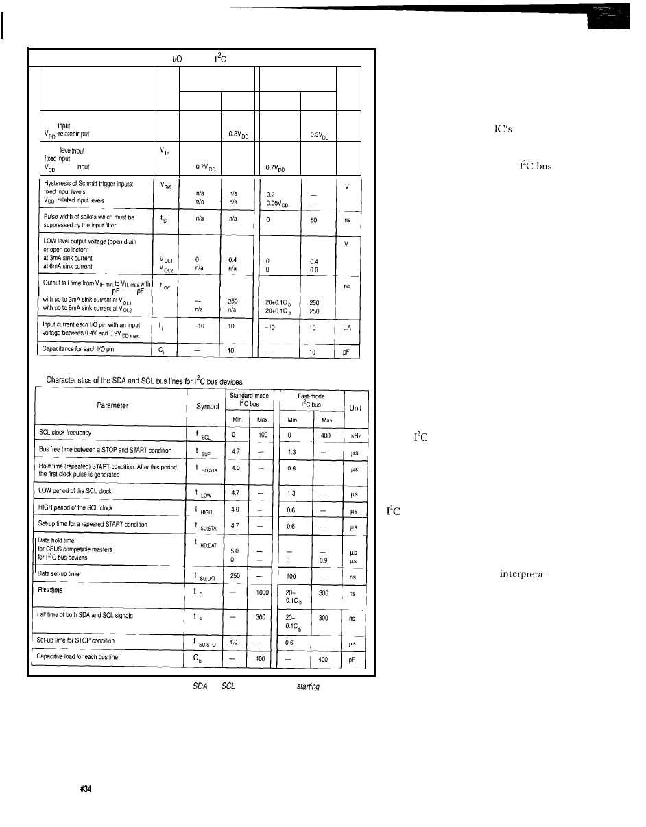
Characteristics of the SDA and SCL stages for
bus devices
internal address, the device configures
itself for the subsequent data transfer
standard-mode
devices
fast-mode devices
Symbol
Unit
Parameter
based on the state of the direction
Min.
Max.
bit.
Min.
Max.
A slave address is made up of two
LOW level input voltage:
“IL
V
fixed
levels
parts [see Figure 4). The first part is
-0.5
1.5
-0.5
1.5
levels
-0.5
-0.5
fixed and is based on the
general
HIGH
voltage:
function. The fixed part of the address
V
levels
3.0
3.0
is the family-type base address. Its
-related
levels
selection is coordinated by the
committee, and is assigned based on
the device’s function. The program-
mable part of the address is selected at
the IC by strapping address pins either
high or low [DIP switches work nicely
for this so that the address of a
functional module, or assembly, can be
easily set). The number of program-
mable address bits is dependent on the
a bus capacitance from 10 to 400
number of pins that can be assigned for
this purpose. The intention of this
addressing scheme is to allow multiple
members of a single classification of
devices to be present on the bus at the
same time. For example, if you have
four fixed and three programmable
address bits, eight devices of the same
family type could be connected to the
bus simultaneously.
In addition to the specific ad-
dresses defined for the various device
types,
defines address 0 as a special
functional address. This address is
referred to as the general call address.
Effectively it is a broadcast command,
and the issuance of this address serves
to select every device connected to the
bus for the coming transmission.
(If a device does not need the data that
is sent as part of the general call
sequence, it can ignore it by not
acknowledging it.) The general call is a
two-byte sequence and its
of both SDA and SCL signals
tion is contained in the second byte.
The meaning of this second byte is
affected by its LSB. If the second byte’s
LSB is 0, then “00000110” is a com-
mand for the slave to reset itself and
accept the programmable part of the
slave address, and “00000100” is a
command for the slave to accept the
Figure 3--A careful study of DC and AC parameters for
and
is necessary before
your design.
programmable part of the slave address
without resetting itself.
denotes a read. The address byte is
Following the recognition of the
If the second byte’s LSB is 1, then
formatted with the actual address left
start condition, each bus member
the two-byte sequence is a hardware
justified; that is, positioned in the
receives and checks the first seven bits
general call and the remaining seven
seven highest bits. The direction bit is
of the address byte for its address. If
bits of this byte contain the address of
contained in the LSB.
this number matches the device’s
the hardware master itself. This could
70
Issue
May 1993
The Computer Applications Journal
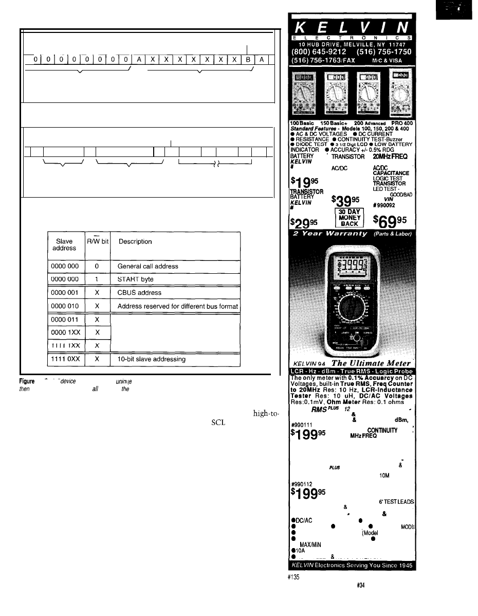
LSB
\
\
First Byte
(General Call Address)
Second Byte
General call address format
(B)
S 00000000 A Master Address 1
A Data
A Data A P
General Call Address
Second Byte
(in Bytes + Acknowledge)
Data transfer from a hardware master-transmitter
Definition of bits in the first byte
Reserved for future purpose
4-Each PC
on the bus has a
network address. When the slave address specified is zero,
fhe packet is recognized by slaves on
bus.
be
used, for example, in the case of an
intelligent device such as a keyboard
which could not be programmed with
the address of the slave device. In such
a situation, the only recourse for the
transmitter would be to generate a
general call and append its own
address in order to identify itself. This
information would then be recognized
by the system controller which would
properly route the data to its final
destination.
ARBITRATION PROCEDURE
All masters generate a clock signal
on SCL to coordinate the data transfer.
As I mentioned, clock synchronization
is performed using the wired-OR
characteristics of the SCL line. As the
transfer sequence progresses, a
low transition on
initiates the
counting of the low period and once
this count expires the device will
allow SCL to go high. If it happens that
another device is holding SCL low, the
actual state of the clock line will not
change. This condition is recognized
by the device driving the pin high.
What happens then is the device that
put its SCL line high will now enter a
wait state that will not terminate until
the other devices driving SCL low
finally release the line to a high state.
Subsequently, the first device that
completes its high time will again pull
SCL low. This synchronization
TEST
990097
100 Basic
TEST
990090
150 Basic+
CAPACITANCE
CURRENT
KEL YIN
1990091
200
Advanced
COUNTER
CURRENT
VERIFY
KEL
PRO
400
TRUE
Model 94
ENGINE
ANAL YZER
Model 95
INSTRUMENTS IN ONE
AC DC VOLTMETERS,
AC DC CURRENT,
OHMMETER, DIODE TESTER
AUDIBLE
TEST,
20
COUNTER,
CAPACITANCE METER,
INDUCTANCE METER,
LOGIC PROBE
Standard Features
plus
TEMP. TACHOMETER
DWELL ANGLE TESTER,
DUTY CYCLE,
OHM
IMPEDANCE, ANALOG BAR
GRAPH, K-TYPE TEMP
PROBE, ALLIGATOR CLIP
TEST LEADS, INDUCTIVE
PICKUP CLIP,
DELUXE CARRYING CASE
Standard Features Models 94 95
VOLTMETERS
AC/DC CURRENT
OHM METER DATA HOLD RELATIVE
FREQ COUNTER to 4 MHz
95)
AUDIBLE CONTINUITY TEST
DIODE TEST
l
AVERAGE MEMORY RECORD
HIGH-ENERGY FUSE PROTECTION
AUTO SLEEP
AUTO POWER OFF
The Computer Applications Journal
Issue
May 1993
7 1
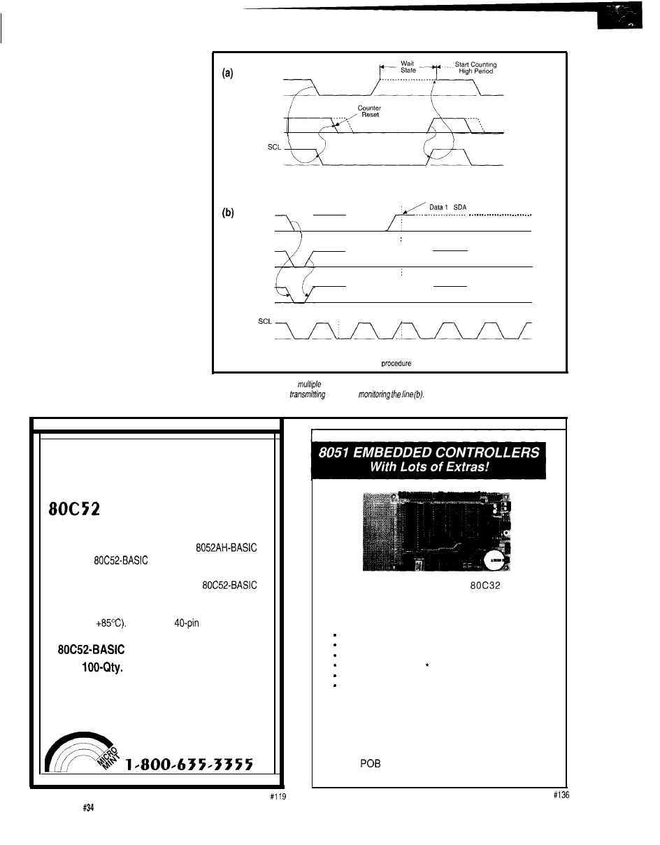
continues on a bit-by-bit basis. This
effectively keeps the clock lines of all
the active masters in sync. Since this
CLK
1
method effectively maintains a
synchronized clock, the actual arbitra-
tion for bus ownership takes place on
the SDA line.
Two or more masters may
CLK
2
generate a start condition at the same
time. Arbitration takes place on the
SDA line when SCL is high. What
happens is that when a master trans-
mits a high, while another master
transmits a low, it discerns that the
state of SDA has not changed and
Data
Clock synchronization during the arbitration procedure
Transmitter 1 Loses Arbitration
drops off the bus. That is, if the level
,
\
Data
of the data line doesn’t match the level
2
\
of the transmitted bit, the high man
bows out.
SDA
This process can continue for a
\
number of bits before the comparison
fails. If both masters are trying to
address the same device, the arbitra-
tion will continue into the actual data
portion of the message. This method of
Arbitration
of two masters
using both the address and data for
arbitration ensures that no loss of data
Figure 5-When there
are
masters on the same bus, they must arbitrate for control. After synchronizing
will occur.
clocks
(a), each begins
while a/so
When one detects a difference, it backs off
and either drops off the bus or becomes a slave receiver.
MOVE OVER INTEL
MICROMINT SOURCES
CMOS BASIC CHIP
Micromint has a more efficient software-compatible
successor to the power-hungry Intel
chip. The
chip was designed for indus-
trial use and operates beyond the limits of standard
commercial-grade chips. Micromint’s
chip is guaranteed to operate flawlessly at DC to
12 MHz over the entire industrial temperature range
(-40°C to
Available in
DIP or PLCC
chip
$25.00
OEM
Price
$14.50
BASIC-52 Prog. manual
$15.00
MICROMINT, INC.
4 PARK ST., VERNON, CT 06066
TO ORDER CALL
We offer a full line of low cost
e m b e d d e d
controllers and software tools which are ideal for
developing products, test fixtures and prototypes.
Features Include:
Low power CMOS design
Up to 60K of code space and up to 60K of data space
5 to 15 volt operation
Small form factor (3.5” 6.5”) with prototyping area
System diskette includes application notes
Start at $100
Available Options:
l
Multifunction Board adds A/D, 24 I/O lines and more!
l
BASIC-52 or Monitor/Debugger in EPROM,
l
C Compiler $100 or BASIC Compiler for $300
Iota Systems, Inc.
8987
l
Incline Village, NV 89452
PH: 702-831-6302
l
FAX:
702 831-4629
72
Issue
May 1993
The Computer Applications Journal
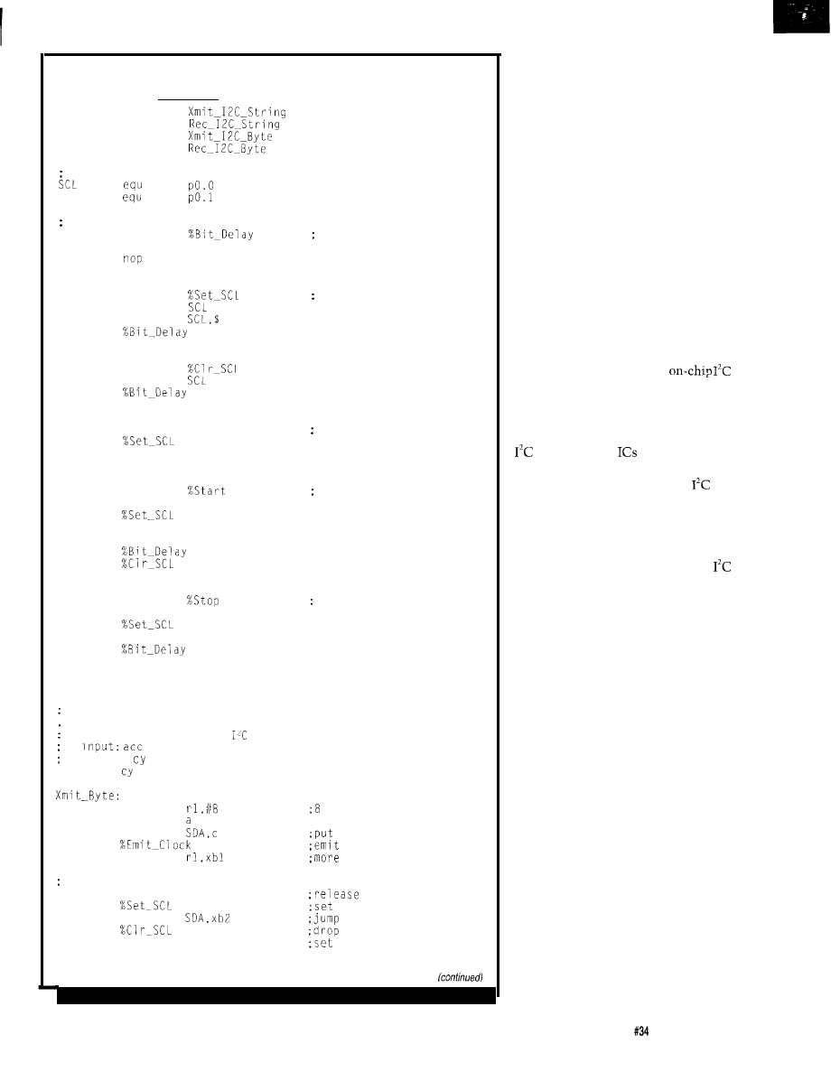
Listing l--When you’re using a processor that doesn’t have a hardware PC interface, often the easiest way
to add one is with software. While more processor intensive, it can be the cheapest solution
public
public
public
public
Port I/O bits
SDA
Macros...
MACRO
nop
ENDMAC
MACRO
setb
jnb
ENDMAC
MACRO
clr
ENDMAC
MACRO
%Emit_Clock
%Clr_SCL
ENDMAC
MACRO
setb
SDA
clr
SDA
ENDMAC
MACRO
clr
SDA
setb
SDA
ENDMAC
Bit Delay
Set SCL
; Clear SCL
Pulse SCL
Start Sequence
Stop Sequence
RSEG
CODE
Subroutines...
Transmit a byte over the
bus
contains byte to transmit
output: = 0 if sequence completes
= 1 if unable to transmit
mov
bits to send
xbl:
rlc
mov
bit on pin
djnz
clock pulse
bits to transmit?
set up to accept ACK from slave device
setb
SDA
SDA
SCL
jnb
if ACK seen
SCL
setb
C
error code
ret
A special case exists if a master
also possesses the slave capability and
loses arbitration during the address
phase. Here, it’s possible that the other
master is trying to address it and the
losing master must immediately
switch over to its slave mode and
become the receiver.
Figure 5 illustrates the arbitration
procedure between two masters. As
you can see, as soon as there is a
difference between the transmitted
data and the state of SDA, the losing
master shuts off its data line and drops
off the bus, or becomes the slave
receiver depending on the situation.
THE QUICK AND
THE INTELLIGENT
Microcontrollers with
hardware can be programmed to be
interrupted in response to activity on
the bus. This functionality can also be
obtained using specifically designed
bus controller
that interface to
standard microcontrollers. Of course,
it can be taken for granted that
peripheral chips are always live (that is
as far as continuously monitoring bus
activity is concerned).
If you decide to interface your
controller as a slave directly to the
bus using a strictly software means,
the state of the bus must constantly be
checked using software polling. Here,
as is often the case, the intelligent
operation of a microcontroller is no
match for pure hardware. This bus
polling activity can consume a lot of
time that could be better spent doing
more useful functions. The problem
can be alleviated, to a great extent, by
using a special start procedure that is
much longer than normal.
The special start procedure is
accomplished by sending a standard
start sequence followed by a special
start byte which consists of the binary
pattern 00000001. In this case, the
receiving controller can sample SDA at
a low rate until one of the zeros is
detected. Once the low level is sensed,
the controller can switch to a higher
sample rate to find the repeated start
condition before normal communica-
tions commences.
This sequence causes no problems
for hardware-based receivers since they
The Computer Applications Journal
Issue
May 1993
7 3
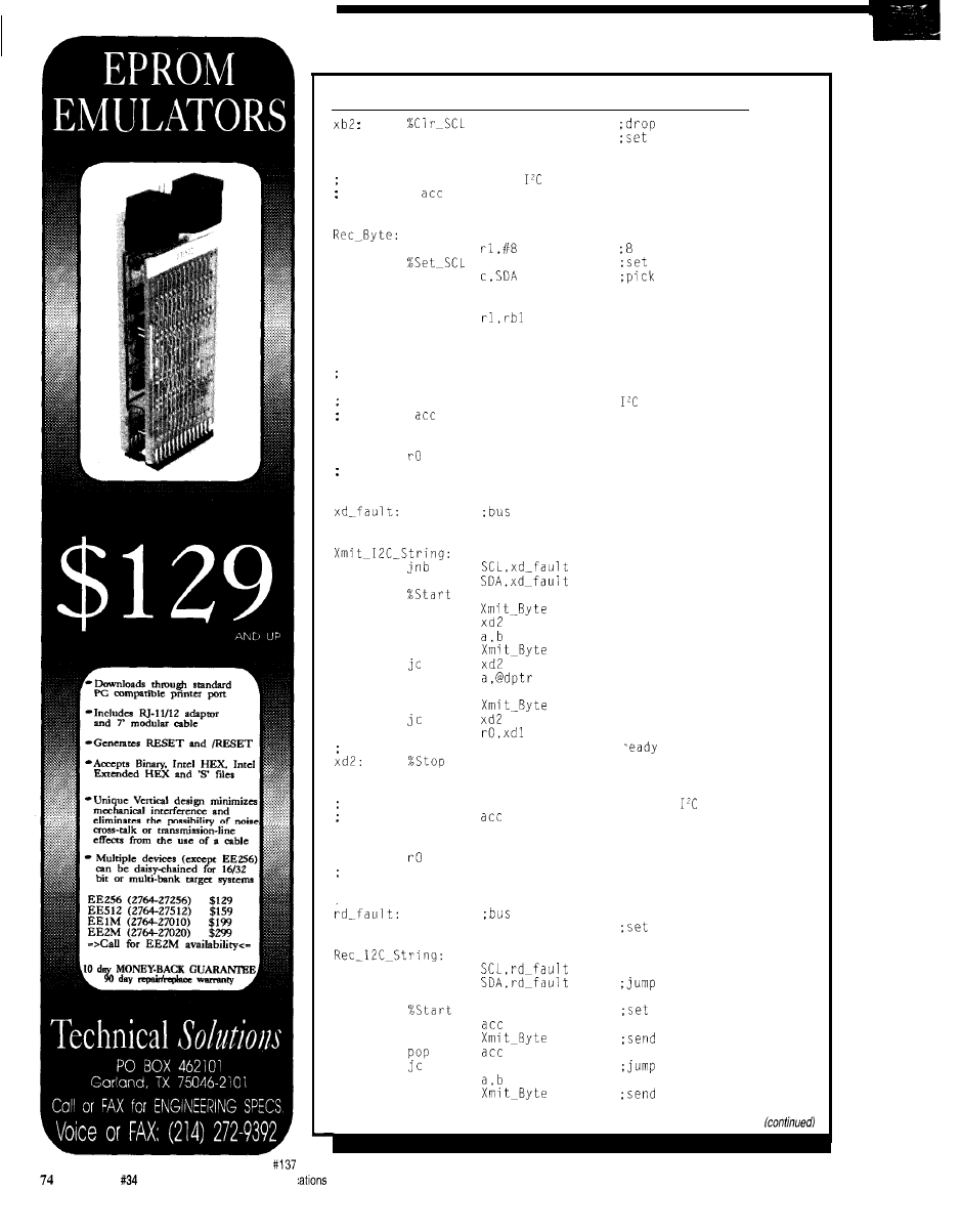
Listing l-continued
SCL
clr
C
complete code
ret
Receive a byte over the
bus
output:
contains received byte
cy is dummied up with a 0
niov
rbl:
mov
rlc
a
%Clr_SCL
djnz
clr
C
ret
bits to receive
SCL
up data bit
drop SCL
more bits to receive?
must complete ok!
Public routines...
Transmit address and data bytes over
bus
input:
contains slave address
b contains register address
dptr points to source buffer
contains byte count
output: cy = 0 if sequence completes
cy = 1 if unable to transmit
fault
setb
C
ret
jnb
call
jc
mov
call
xdl:
movx
inc
dptr
call
djnz
set stop condition, return code
ret
is al
set error code
jump if bus fault
set start condition
send slave address
jump on error
send register address
jump on error
pick up data byte
send data byte
jump on error
more bytes to send?
in cy
set stop condition
Transmit address and receive data bytes over
bus
input:
contains slave address
b contains register address
dptr points to destination buffer
contains number of bytes to receive
output: cy = 0 if sequence completes
cy = 1 if unable to receive
fault
setb
C
error code
ret
jnb
jnb
if bus fault
start condition
push
call
slave address
rd3
on error
xch
call
register address
Issue
May 1993
The Computer Applic
Journal
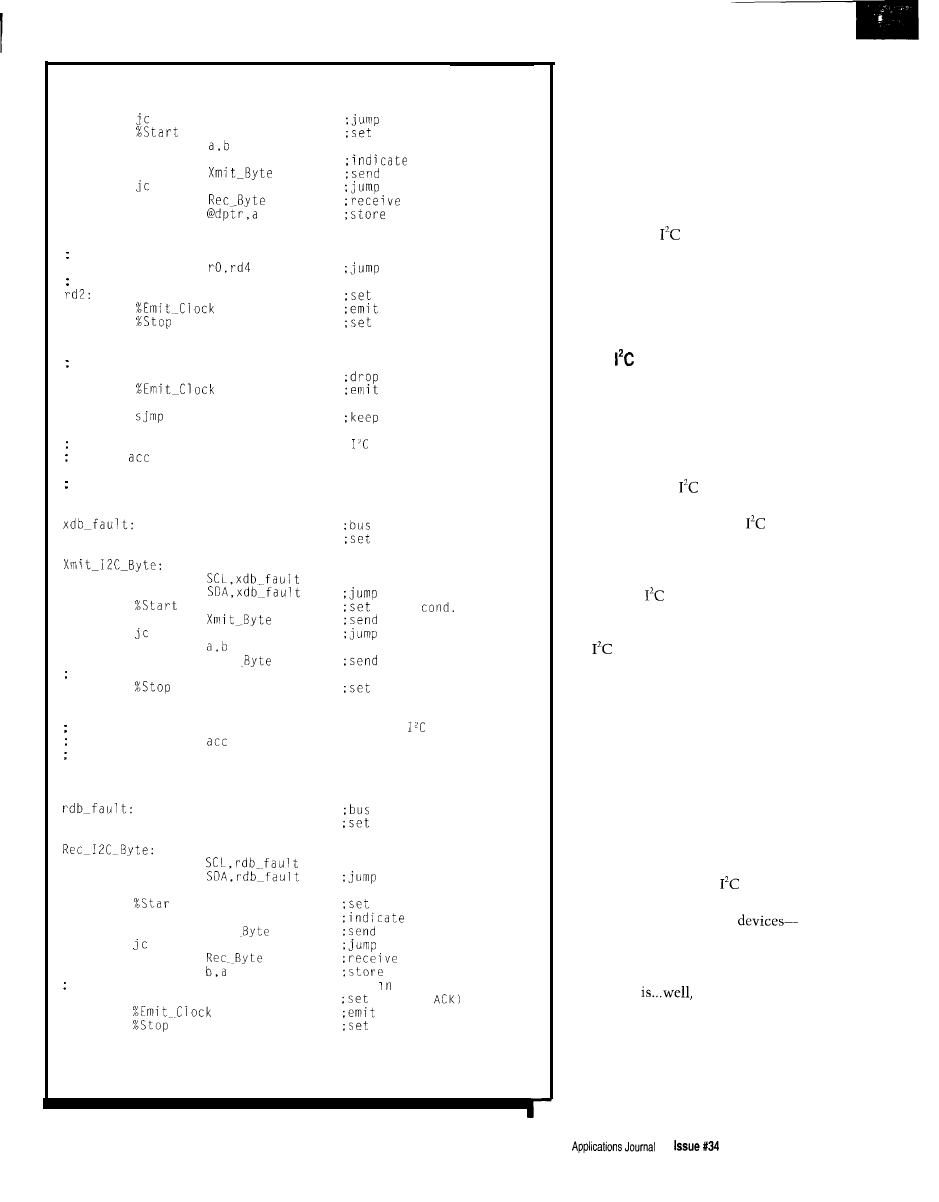
Listing l-continued
rdl:
rd3
on error
repeated start
mov
setb
acc.0
call
read operation
slave address again
rd3
call
on error
data byte
movx
inc
data byte
dptr
Send ACK on all but last byte
djnz
sequence complete,
if not last byte
return code is already in cy
setb
SDA
SDA (no ACK)
rd3:
clock pulse
stop condition
ret
send ACK and continue receiving
rd4:
clr
SDA
the Ack bit
setb
clock pulse
SDA
rdl
receiving
Transmit address and a data byte over
bus
input:
contains slave address
b contains data byte
output: cy = 0 if sequence completes
cy = 1 if unable to transmit
fault
setb
C
error code
ret
jnb
jnb
if bus fault
start
call
slave address
xdbl
on error
mov
call
Xmit
data byte
set stop condition,
xdbl:
return code is already in cy
stop condition
ret
Transmit address and receive a data byte over
bus
input:
contains slave
output: b contains received byte
cy = 0 if sequence completes
cy = 1 if unable to receive
setb
ret
jnb
jnb
setb
call
call
mov
acc.0
Xmit
rdbl
address
fault
error code
if bus fault
start condition
read operation
slave address
on error
data byte
data byte
sequence complete, return code is already cy
setb
SDA
SDA (no
rdbl:
clock pulse
stop condition
ret
will reset on the repeated start condi-
tion and will ignore the start byte.
Note that an acknowledge-related
clock pulse is generated after the start
byte. This is a dummy clock that
exists only to conform to the standard
data format on the bus and no device
should attempt to assert an acknowl-
edgment.
Although
defines even more
capabilities, 1’11 not belabor this any
further. I’m sure by now you can
appreciate the capabilities that have
been imparted to these two wires by
the designers.
SOFT
So, now you have a serial bus
architecture that supports multimaster
communications, a bunch of special
features, and looks like it’s set up to
handle just about any eventuality. As I
mentioned, you can get microcontrol-
lers with built-in
hardware
support. If none of these suit your
taste, you can get dedicated
controllers that can be lashed to just
about any processor you like. With all
this available hardware you can easily
tap into the
feature set. What do
you do next!
Well, in spite of the capabilities of
the
bus, a lot of people will be
content to just run the whole thing
under control of a software loop. The
fact that this is feasible, confirms the
architecture’s flexibility. Taking this
approach, you would most likely only
use a fraction of the capabilities of the
bus. But a little may be all you need.
While this can be a restrictive ap-
proach, as far as CPU utilization is
concerned, it opens up a lot of periph-
eral functions at the cost of just two
pins.
The software-based
driver loop
I’m presenting here is designed to
interface to block-oriented
that is, devices that have addressable
registers. I’m sure you can see that
adapting these to handle simple
peripherals
simple. Basic
block read and write operations are
supported with slave addressing and
register addressing support built-in.
Let me begin by briefly describing the
code starting from the smallest
component parts.
The Computer
May1993
75
The macros appearing at the start
of the listing should be pretty self
explanatory. My motive in coding the
fundamental functions as macros was
primarily driven by a desire to keep
the source code as simple and unclut-
tered as possible. I found out that the
software implementation of the
protocol was not quite as clean as 1
would have liked, so I tried to encapsu-
late the ugliness as much as possible.
The subroutines that follow
should also be clear in their intent.
They simply handle the signaling on
the pins to effect the data transfers;
transmitting and receiving bytes. Here,
the embedded macros hopefully make
the code a bit more readable. You will
notice that I use the carry bit as a
success/fail indicator. This indicator is
conveyed up to the application layer.
Status information is useful in identi-
fying bus faults and malfunctioning
peripherals. Indeed, this is an old trick
whereby you can defer from directly
handling the possible error conditions.
Let the more intelligent code go at it!
Divide and conquer!
Finally, the public transmit and
receive routines handle the details of
framing the transactions with the start
and stop sequences and manage the
peripheral’s addressing requirements.
The register selection procedure for
the write function is handled by first
sending the obligatory slave address to
select the chip and then writing the
register address. Following this, the
data is immediately written to the
slave. Reading requires the same
initial sequence, but following this, a
repeated start condition must be
asserted. The slave address is again
presented, but now a read operation is
indicated (LSB=O). Following this, data
can be streamed from the peripheral.
In both cases the byte count for the
operation is held in r
d p t
r is the
source or destination pointer as
appropriate. Note that the routines
allow writing or reading multiple
bytes. This is possible since most
registered peripherals have an
increment capability that bumps up
the internal register address generator
at the conclusion of each write or read.
WRAPPING UP
It’s always a good idea to cover
some theory when exploring a new
topic, but it’s equally important to
apply it. Right now I’m rounding up a
bunch of
peripherals and control-
lers. Next time I’ll have some of this
stuff wired up. I’m hopeful I can get it
to do something useful.
q
Dybowski is an engineer in-
volved in the design and manufacture
of hardware and software for indus-
trial data collection and communica-
tions equipment.
Signetics Company
811 E. Arques Ave.
P.O. Box 3409
Sunnyvale, CA 94088-3409
(408) 991-2000
419
Very Useful
420 Moderately Useful
421 Not Useful
1
The Circuit Cellar Project File, Volume 1 has over 200 pages
of new and expanded hands-on projects and tutorials.
The Computer Applications Journal’s editors have chosen a dozen
of the top projects from the Circuit Cellar Design Contest, inde-
pendent submissions, and top-response articles to make a book
with something for every interest!
now only
l
(Includes domestic delivery*)
Order
your copy today!
‘$17
95 Visa, Mastercard, Check, or Money Order (US Funds
(Add for
Canada Mexico, $4 00
other non-U.S. addresses)
V o l .
4 Park Street, Vernon, CT 06066 Tel: (203) 875-2 199
l
Fax: (203)
7 6
Issue
May 1993
The Computer Applications Journal
TALK
by Russ Reiss
rapidly evolving area of technology. These abstracts range
from a couple of fundamental patents in multimedia and
virtual reality to design techniques for enhancing, speeding
up, and compressing video and transmission of video
information in television format.
Two of the most talked about (and esoteric) areas in
computer video these days are multimedia and virtual
reality. The first two patents demonstrate moves to get
early footholds in these emerging areas. Abstract
1
presents
a
multimedia interface approach that very simply and
flexibly piggybacks multimedia onto existing text-only
applications. The idea is to have the software send
be realized only if it were to become a standard that allows
a wide variety of multimedia devices and software applica-
tions to coexist harmoniously.
Abstract 2 provides a similar “fundamental” capability,
but in the field often known as virtual reality. For a wide
range of applications, and specifically in military displays, it
is necessary to superimpose images of real-life scenes and
computer-generated objects. For the resulting image to look
realistic, it is crucial that three-dimensional placement and
between the two video sources be matched.
While the abstract does not present the actual techniques
used, it begs the reader to review the entire patent to see
what novel approaches might be used. I’ve discussed in past
columns how to get complete patents.
The next three patents relate to generation, control,
and manipulation of computer graphics images. The first,
by Philips Corporation, presents a hardware approach to the
hidden-surface removal problem which would offer
fast performance. As Abstract 3 explains, normal x, y, and
color data are augmented by storage of z (depth) information
mands to multimedia playback units in parallel with the
in video memory. Essentially, a special-purpose graphics
textual data. In this manner, the current text-only
processor-most likely incorporated within a graphics
tion is augmented with additional speech and video images.
controller chip design-uses these data types to determine
I
would suspect that the full power of such a scheme would
whether or not new data should be written to video RAM.
Patent Number
Issue Date
Inventor(s)
State/Country
Assignee
US References
1990 06 05
Isle, Brian A.; Bloom, Charles P.; Butler, Arch W.; Spoor, David; Wunderlin, David J.;
Bedros, Renee
M N
Electric Power Research Institute
6,208
US Class
3641513
.Ol 3641579 3641514 3641200 3641274.7 3641275.7
10
Int. Class
1
Title
Multimedia interface and method for computer system
Abstract
A multimedia interface presents information and receives user commands for a computer system. The multime-
dia interface operates in parallel with another application software module, such as an expert system. To add
multimedia features to the application software module, the module is modified so as to generate multimedia
commands at the same time as it displays text on a text monitor. The multimedia commands, which are held in a
queue, provide additional information in the form of video images and generated speech corresponding to the
displayed text. In addition, the multimedia commands are split into at least two sets: one set which is dispatched
to the user substantially immediately after displaying the corresponding text, and one set which is dispatched
only upon request by the user. In the preferred embodiment, the multimedia interface presents information to the
user through text, graphics, video, speech production, and printed output. User inputs are made through a
special- function keypad and voice recognition. The preferred embodiment is a portable expert system which fits
in a single portable suitcase-sized package.
78
Issue
May
1993
The Computer Applications Journal
Patent Number
Issue Date
1990 11 13
Inventor(s)
State/Country
Assignee
Welsh, William T.;
Kenneth
NC
Land Development Laboratory, Inc.
US References
US Class
Int. Class
3641522 3641521
Title
Computerized video imaging system for creating a realistic depiction of a simulated object in an actual environ-
ment
Abstract
A system and method for producing highly realistic video images which depict the appearance of a simulated
structure in an actual environment, and provides for accurate placement of the structure in the environment and
matching of the perspective of the structure with that of the environment so that a highly realistic result is
achieved. The system includes a video input means, such as a video camera and video recorder, by which a
video image of the actual environment may be captured. A graphics processor unit receives the video image
from the video input means and stores it in rasterized form. Field data input means is provided for receiving field
location data regarding the precise location of the captured video image and field perspective data regarding the
perspective of the captured image. Object data input means is also provided for receiving data, such as CAD
data for example, for a three-dimensional model of a simulated object which is proposed to be included in the
environment. From the three-dimensional model of the object, a two-dimensional perspective representation of
the object is generated, which accurately matches the perspective of the captured video image. The thus
generated two-dimensional perspective representation is then merged with the rasterized video image and
accurately positioned at its proper location in the environment.
Patent Number
Issue Date
Inventor(s)
State/Country
Assignee
1990 05 08
Winser, Paul A.
GBX
US. Philips Corporation
US References
US Class
Class
3641522 3641521 3641518 3401750
Title
Apparatus for modifying data stored in a random access memory
Abstract
Input data defines the address
and an input color (RGB) and depth (Z) for a picture element (pixel) within a
stored image. In order to perform hidden-surface removal (HSR), current depth values are stored for each pixel
and compared with the input depth value to determine whether or not input data should be written to define a
new color and depth for the pixel at
The color and depth values are stored in a color RAM (9) and z-RAM
(64). To obtain a speed advantage when modifying a series of consecutive pixels and one row of the
the
current depth values are read and compared in advance for each pixel, during the writing period of one or more
preceding pixels. The apparatus comprises a control and arithmetic unit
and an HSR control circuit (60) in
addition to the color RAM (9) and z-RAM (64). The apparatus uses readily available video DRAM chips to
provide a z-RAM with two data ports
The apparatus may form part of an electronic graphics system.
The Computer Applications Journal
Issue
May 1993
7 9
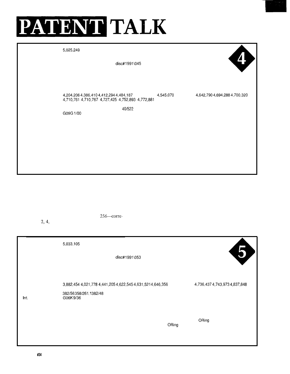
Patent Number
Issue Date
Image Disc #
Inventor(s)
State/Country
Assignee
US References
1991 06 18
This patent is on Patentlmages
Seiler, Larry D.; Pappas, James L.; Rose, Robert C.
MA
Digital Equipment Corporation
43542,376
4550,315
US Class
3401721 3401723 3401729 3401734
3641522
Int. Class
Title
Pixel lookup in multiple variably sized hardware virtual color maps in a computer video graphics system
Abstract
This invention adds a window-dependent base value to the pixel values read from a frame buffer or other source
of pixel values. The base value points to the base of the color map for that window, which is allocated within a
larger, physical color map. Each window can access physical color map entries starting at its base value and
extending up to the base value plus the maximum pixel value used in that window. Adding a window-dependent
base value to the pixel values for each window allows different windows to use different color maps, each of which
can be allocated to any contiguous set of entries in the physical color map. Each window’s virtual color map need
only use as many entries in the physical color map as there are entries in the virtual color map. Finally, virtual
color maps can be compacted or otherwise reallocated in the physical color map without requiring changes in the
pixel values stored in the frame buffer. Only the color map base values stored for each window need be changed.
Pixels representing points physically behind other pixels (at
a greater z-value) would not be written.
The DEC patent shown in Abstract 4 provides a
hardware means for achieving enhanced and potentially
more dynamic and interesting displays within a windows
environment. Normally, the entire display screen is limited
to a given number of colors (often 4,
16,
or
sponding to
or 8 bits per pixel) even though these
pixels may be chosen from a larger color palette. This
invention permits each window to use its own set of colors
chosen from the large palette. In this manner, for example,
the compact memory utilization of four-bit color mode
might be retained while achieving a much more interesting
display in which a different set of
16
colors is used within
each window. Of course, software changes would be
required to store the current window number along with
each pixel. This would offset much of the memory savings,
however it still offers the prospect for strikingly more
Patent Number
Issue Date
1991 07 16
Image Disc #
This patent is on Patentlmages
Inventor(s)
Atkinson, William
State/Country
CA
Assignee
Apple Computer
US References
4 , 7 2 9 , ,127
US Class
382122
Class
Title
Video compression algorithm
Abstract
A method for encoding compressed graphics video information and decoding such information. The method
consists of enriching the video information in zeros through shifting and Exclusive
video with itself. A
number of methods are attempted in the shifting and Exclusive
process in order to determine the method
which yields the optimum zero-enriched image. The zero-enriched image is then encoded and the encoded
information stored. Upon retrieval, the information is decoded and an Exclusive OR and shifting process is done
to obtain the original video information.
82
Issue
May
1993
The Computer Applications Journal
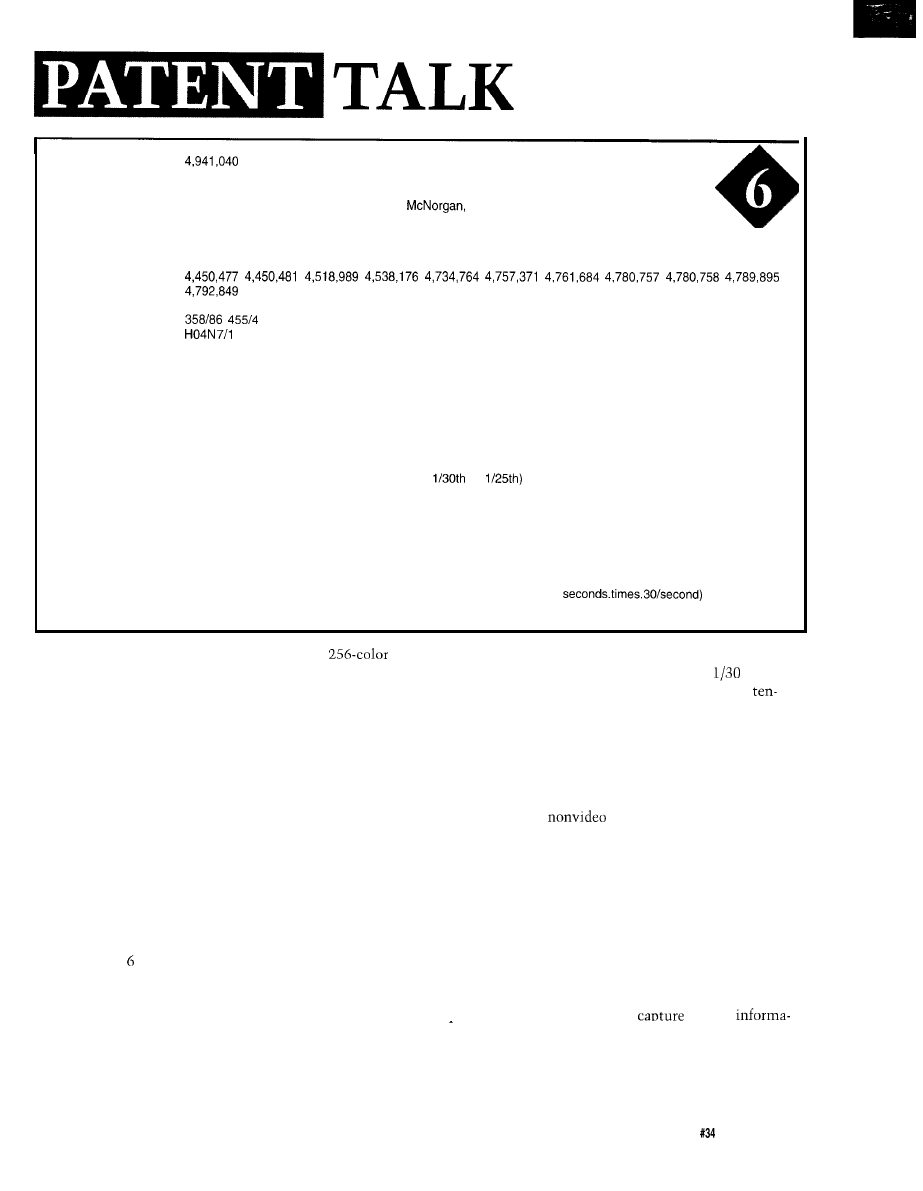
Patent Number
Issue Date
inventor(s)
1990 07 10
Pocock, Terrence H.; Coumans, Peter J.;
Richard M.; Hart, George M.
State/Country
CAX
Assignee
Cableshare, Inc.
US References
US Class
Int. Class
0
Title
Cable television system selectively distributing prerecorded video and audio messages
Abstract
A method of, and a system for, selectively delivering still television video with accompanying audio to home
subscribers over a cable television system for advertising, promotional, or educational purposes. A maximum
number of home subscribers can interactively request presentations of their own choosing to be displayed on
their home television sets. Only one standard television channel is required for transmission of still video with
accompanying audio to serve 300 concurrent users. No equipment is required in the subscriber’s home. The
video is presented as still frames from one of a number of videodisc players, transmitted over one television
channel during the appropriate time interval of
(or
of a second. Such video frames, which may
also contain overlaid graphics information, are uniquely addressed to a remote storage device. Unused
bandwidth is used for the transmission of up to 300 discrete audio messages. The remote storage device
identifies the appropriate video still frame, stores it, combines it with the corresponding audio message and
conveys both to the home subscriber’s television on a preselected channel. By uniquely addressing video
frames to the remote storage device, either 30 (or 25) different video frames per second can be conveyed on
one television channel to 30 (or 25) different remote storage devices for retransmission to home subscribers.
Thus, if a home subscriber sees a given still video frame for 10 seconds, his remote storage device need not be
updated for those 10 seconds, enabling the system to transmit 300 (10
different
video frames to 300 other remote storage devices, thereby serving 300 concurrent users.
dramatic
and useful displays, particularly with
windows.
Apple Computer presents an intriguing patent in
Abstract 5 which presents a novel means of compressing
video data. The raw data is first massaged by an algorithm
that essentially acts like a pseudorandom noise function
(like a feedback shift register] in order to introduce more
zeros into the data. Apparently, a somewhat hit-or-miss
approach is used to find a “good” encoding key by which
the data may be compressed to a greater degree than
without this manipulation. While only the algorithm is
mentioned in the abstract, there would seem to be applica-
tion areas in which a hardware-implemented and pipelined
“zero enricher” followed by a conventional (run length or
other) encoder could rapidly compress video data, perhaps
for transmission as well as storage.
The next two patents relate to video information in TV
form. Abstract presents a method for supplying any one of
many still images (and accompanying audio) to a home TV,
example, if the viewer is content with viewing one image
for 10 seconds, then (since a frame represents
second)
the single channel can carry 300 still images in this
second period. Note that if the requirement permits the
image to be updated only once a minute, then this scheme
could handle 1800 images per channel. Although not
mentioned in the abstract, this scheme could have applica-
bility beyond cable TV. For example, it could be used to
broadcast images within a department store or a factory. It
could also support
information in essentially the
same “frame-multiplexing” manner, because the frame
buffer really doesn’t care what meaning the information
has.
I was a bit surprised to find a patent issued to The
Weather Channel, for we tend to think first of the weather
forecaster on our screen describing tomorrow’s showers
rather than the technology behind the scene. The scheme
shown in Abstract 7 presents a method for centralized
distribution of weather information (video, audio, and data)
to remote receivers in a TV network. The novel scheme not
only permits remote receivers to
just the
for example for advertising purposes via cable. The scheme
sends each “still” in a single TV frame that is stored at the
destination in a frame buffer, from which it is played out to
tion that is pertinent to each, but also for the central
the TV receiver. The number of still images that may be
computer to send command sequence “scripts” to the
carried over a single TV channel depends on how rapidly
receivers to tell them, in effect, what to do. In a sense,
the viewer requires new visual information. Using their
we have here is a multimedia distribution network.
what
The Computer Applications Journal
Issue
May 1993
83
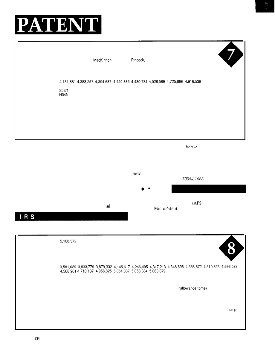
TALK
Patent Number
Issue Date
Inventor(s)
State/Country
Assignee
US References
US Class
Int. Class
Title
Abstract
5140,419
199208 18
Galumbeck, Alan D.;
Russell D.;
Douglas G.; Reid, Frederick A.
GA
The Weather Channel, Inc.
42 3401825.44
71087
Communications system
A communications system having centralized management and multiply hierarchical addressing schemes is
disclosed. The system may be used in connection with supplying video, audio, and data such as weather-related
text, graphics, and information to affiliated receivers in a network for broadcast or display. Receivers may be
addressed singly or in groups and allowed to determine their own addresses from information keyed, directly or
indirectly, to a receiver characteristic such as the unit serial number. Lists of commands denominated “scripts”
and transmitted to receivers are used for controlling the various modes or states of the receivers.
Finally, with video information so pervasive, there
Russ Reiss holds a Ph.D. in
and has been active in
always seems to be the need or desire to restrict someone’s
electronics for over 25 years as industry consultant,
access to
it. Abstract 8 purports to be a novel means of
designer, college professor, entrepreneur, and company
controlling children’s viewing of TV through the use of a
president. Using microprocessors since their inception, he
microprocessor-based, parent-programmable “video control
has incorporated them into scores of custom devices and
system.” Even with its LCD readout, I wonder how many
products. He may be reached on the Circuit Cellar
parents will go through the trouble of programming it
BBS or on CompuServe as
(based on all the complaints regarding the difficulty of
programming VCRs), or how the system knows which child
(and his friends and siblings!) is watching at any given
moment. But wherever a problem is perceived, there is
Patent abstracts appearing in this column are from the
Automated Patent Searching.
database from:
always someone ready to patent a solution to it!
25 Science Park
New Haven, CT 065 11
422 Very Useful
423 Moderately Useful
424 Not Useful
(203) 7865500 or (800) 648-6787
Patent Number
Issue Date
Inventor(s)
State/Country
US References
1992 1201
Sweetser, David J.
c o
Title
Video control system
Abstract
A video viewing control system which permits the parent to enter a viewing
for each child and
which disables viewing of a television by disrupting the television’s Radio Frequency (RF) input signal or video
input signal when the child has watched television for his allowable time. The system includes a single chip
microprocessor and a liquid crystal display which permits display of graphical symbols to the child for easy
comprehension. The system is battery-powered to protect against power outages. The child’s viewing time can
be set on a daily basis (potentially different for each day of the week) or can be done on a weekly basis (a
sum covering the entire week). Block out times (during which television viewing is disabled) can be programmed
for each child on the hour and half-hour for any day of the week. The system calculates and displays each child’s
average viewing time per day and the total viewing time over any desired period.
84
Issue
May 1993
The Computer Applications Journal
The Circuit Cellar BBS
bps
24 hours/7 days a week
(203)
incoming lines
Vernon, Connecticut
A few months back wrote about our new high-speed modems.
We’ve just finished completely rep/acing the rest of the hardware on
which the Circuit Cellar
runs. The combination of the
speed modems, the WK support, and increased usage was really
taxing the older AT-style hardware we had been using. We’re now
running on a
‘386SX with 280 megabytes of disk space. If
you gave up calling because the system response had gone down or
were ho/ding off on that large upload, give if another shot.
The first two threads this month are follow-ups to last issue’s
that issue, Tom Maier asked about the use of a
series resistor with a crystal in a processor oscillator circuit (specifi-
cally, with the Microchip
In the first thread this month, a reader
offers another explanation for that series resistor.
the second thread, another robotics
jumps info the
discussion started last month about robotics’ past and future. This
topic continues to be hot on the
so if you want to join in, if’s not
too late to call.
Next, we have some trials, tribulations, and tips from someone
who’s been through FCC (and other agency) testing and lived to tell
about it.
Finally, we look at what’s involved in frying to make a toy car
follow a buried guide wire.
Crystals and series resistors
From: BILL HAWKINS To: TOM
Tom, I saw your question about the series resistor in
have just had occasion to “discover” the
reason for series resistors with crystals; up to now I had not
used them either. We recently took an embedded system
through FCC approval. It had only one oscillator circuit,
using a 24-MHz crystal. We had wild emissions at 120.00
MHz, which sure surprised us. The guy running the test
thought that this noise was the fundamental frequency,
since there were no emissions at 60 MHz.
After a long weekend worrying about the problem, I
remembered something about square waves and odd
harmonics. Sure enough, 120 is a 5th harmonic of 24. The
problem was the square wave on the crystal. The atmo-
spheric coupling of the circuit peaked around 120 MHz,
thus our radiated noise. You can’t get rid of the harmonics
and still have a square wave, so the only thing you can do is
by Ken Davidson
lower the amplitude. This is where the series resistor comes
in. Instead of banging a square wave at 5 V, the resistor
lowers it to somewhere around 2 V (in our case.) Of course,
this means the crystal is no longer a digital signal. The
drive circuit actually runs in linear mode. You still have to
hit the proper thresholds to make the circuit switch though.
We used a series resistor, and this put our amplitude
in the mud. This also prevented the circuit from oscillating.
The fix for that is a parallel resistor across the crystal
in our case). This resistor biases the circuit to ensure
oscillation. Higher values of series resistor result in
amplitude oscillations. The parallel resistor, carried to 0
ohms, would oscillate at the propagation frequency of the
crystal driver, so it must be a fairly high value to keep from
overwhelming the crystal. It also must be low enough to
help the crystal swing over the input threshold. You aim at
an amplitude high enough to prevent stray noise from
affecting oscillation, but low enough to prevent radiating
odd harmonics to the world. Hope this helps..
From: TOM MAIER To: BILL HAWKINS
Well, I hadn’t thought about radiated noise as the
reason for the series R. The series R
decrease the
harmonics on the oscillator. What is confusing to me is the
Microchip data sheets say the crystal manufacturer would
recommend the value of the series R. This seems silly to
me. How would they know? It would be a function of the
oscillator, and Microchip made the oscillator.
Increasing the series R would cause more rounding of
the edges of the square wave, thus reducing the amplitude
of the 5th harmonic and the emitted signal. This is due to
RC filtering of the feedback of the oscillator.
I have the feeling this has to do with the power han-
dling capability of the oscillator in the PIC. If the crystal
feedback is too strong, then it blows the oscillator.
You are right about the harmonics, but I think there is
some other answer needed here concerning the power
handling capability of the oscillator and/or the crystal.
From: BILL HAWKINS To: TOM MAIER
am using a Xilinx part, and they say the same thing..
The series R may be needed, consult crystal manufacturer..
The Computer Applications Journal
Issue
May 1993
8 5
I did talk to our crystal FAE, he didn’t know anything about
it. Then he checked some of his modem applications, and
found the series R and the explanation that it was for FCC
compliance. I have never heard of overloading an oscillator
circuit with a crystal, but then I suppose anything’s pos-
sible. I only thought it may be the same problem because
both manufacturers used the same verbiage. I think they
send you to the crystal manufacturer only because they
don’t want to have to deal with it. It really is more a system
problem than a crystal or oscillator constraint. I think the
proper R is much more dependent on board layout and
choice of damping capacitors.
Robotics musings
From: ROBERT NANSEL To: WALTER BANKS
Asking “What happened to robotics?” is like asking
“Whatever happened to kids these days!” In other words,
the question is too general; robotics isn’t a monolithic
industry (never was). You have to separate the maturing
(i.e., boring) industrial-style manipulator market from the
emerging (i.e., exciting!) mobile service robot market. They
are
different animals.
First, mobile service robots are a harder sell. It isn’t
easy finding truly economic uses for mobile robots. Right
now the field is pretty much limited to office mail delivery,
hospital meal delivery, warehouse security, nuke plant
maintenance, and bomb disposal. The common thread
among all of these is they are all applications where cost
isn’t the overriding consideration and the robot’s domain is
controlled and limited.
For example, TSR, a company in Connecticut, makes a
machine they call the
for hospital meal delivery.
The
is about the size of a washer or dryer, weighs
more, and is one dazzling bundle of technology. When
Mendelssohn and I visited TSR’s facility in Danbury last
September, I was fabulously impressed with the machine.
Here they’ve really
solved the tough problems of
autonomous navigation.
The only concession they make in the environment for
the robot is to put a foot-long piece of 3M reflective tape on
the ceiling at
location in their office suite. The
uses that as a benchmark to fix its position at the
start of its rounds. It uses no buried wires to guide it, no UV
bar codes on the ceiling, no IR beacons to mark doorways.
The
instead relies on an internal CAD model of
the floor plan, a host of ultrasonic and IR obstacle detectors,
dead reckoning, and the deft use of structured light projec-
tion to reduce the data it must crunch from its CCD
camera. It’s designed to navigate a known environment
consisting of corridors, elevators, and doorways.
The various subsystems of the
are controlled
by satellite
processors networked by an RS-485
multidrop scheme. A
waves the baton for the
1
chips. Interestingly, they chose a ‘386 motherboard to do
the vision processing from the CCD IR camera. The ‘386 is
able to handle this task because they use structured light
(two
strobes with focusing optics to create horizontal
fans of IR filtered light). One projector is mounted low,
about 12 inches off the floor, the other a bit higher at about
18 inches. They pulse the strobes alternately about five
times a second.
The IR camera, mounted inside the robot above the
strobe projectors, looks forward and down at about a
angle. Its field of view covers a patch of floor between three
and fifteen feet in front of the robot. What the camera
sees when the robot is in a corridor is a binary image with
two sets of converging stripes (the walls of the corridor)
alternating between 12 and 18 inches from the floor. If there
is no obstacle in front of the robot, that’s all it sees. If there
is an obstacle at least 12” tall, the robot will see a contour
that disrupts the straight light stripes. If a doorway is
present, the robot will see that as a discontinuity in one of
the straight light stripes. Using this method, they so reduce
the amount of data that needs to be passed off to the master
68k processor, that the ‘386 is interfaced to the multidrop
network through an
I. The robot can make free-space
calculations (that is, determine where there is room enough
for the robot to pass) in something like 20 milliseconds.
That’s right-it navigates in
time.
Anyway, I mention all of the above to drive home a
point. The
is state of the art. I know of no other
system that can touch it. It costs something like
if
you wanted to buy one. Mostly TSR leases them to hospi-
tals for the strategic amount of
24 hours a day,
days a year. In-the-field experience in real hospitals shows
over 98% successful trip completion. For their market, the
will ultimately be successful because it makes
economic sense. But..
is a lot of money. There are few groups and even
fewer individuals who can contemplate spending that much
for production models [not to mention
without an
-extremely_ clear idea what the market is.
So, mobile service robotics is in the classic
and-egg problem of there being no money to develop mobile
robot technology until a market is established, but a market
can’t be established until there are robots developed that do
something that folks need doing, and developers don’t know
what that killer application might be, so round you go.
The thing freezing out most tinkerers from just blindly
whipping together a robot and throwing it on the market to
86
Issue May
1993
The Computer Applications Journal
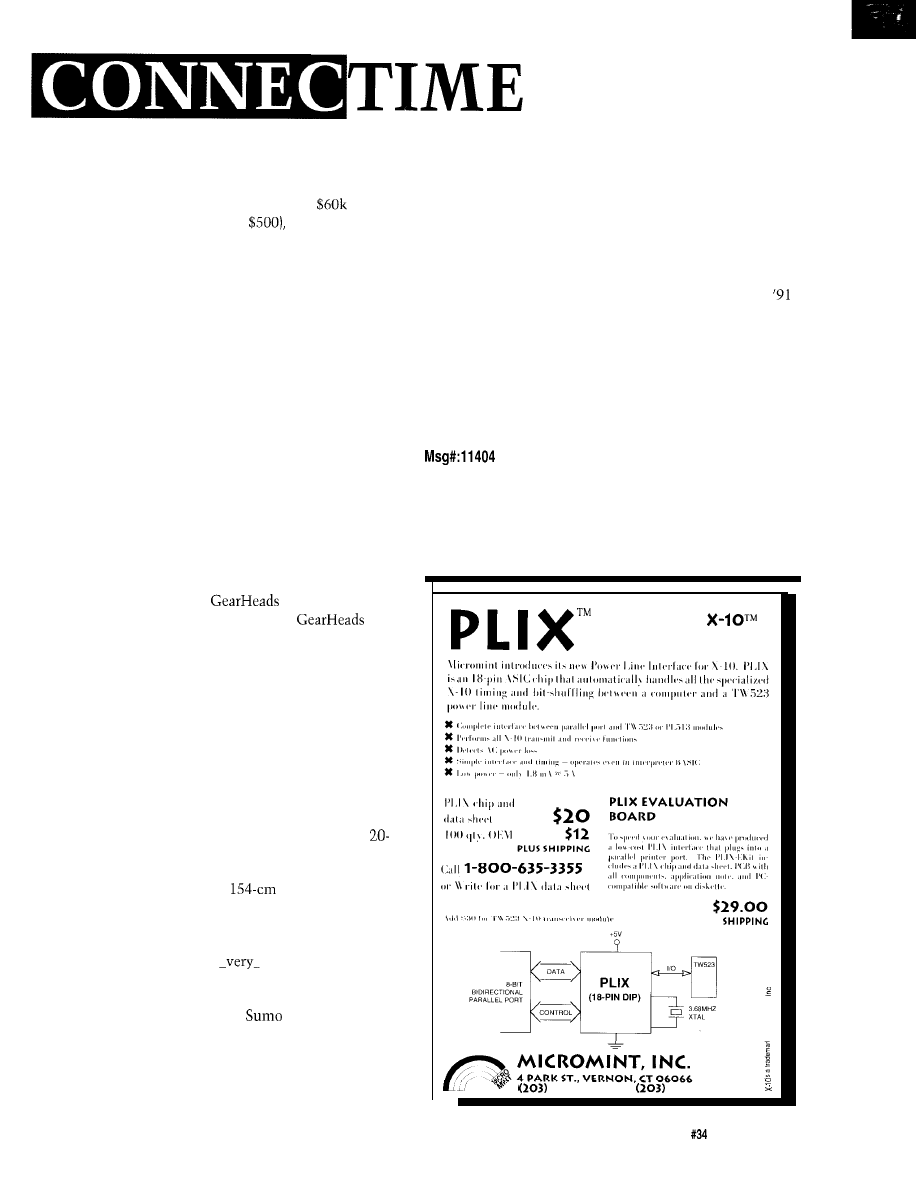
see what happens is cost. If we can find an application that
inherently requires low-cost hardware, where the entry
costs can be something more reasonable than
(say
under $1000, but preferably under
then we’ll see a
level of experimentation and development that will allow
us to eventually stumble onto the VisiCalc or PageMaker of
mobile robotics. What would that first low-cost application
be? My guess is it will be some kind of robotic sport/hobby.
Consider the situation with R/C model cars, boats, and
planes. Here is a market with millions of units moved each
year. The average R/C modeler sinks, say, $400 into one
model, probably owns more than one model, and will
probably buy another model within the coming year. If you
doubt the viability of this marketplace, thumb through an
R/C modeling magazine some time or visit a hobby shop.
Just the number of retail hobby shops catering to this
market in any metropolitan area will give you a feel for the
size of the market.
OK. The task then becomes finding something that
mobile robots can do that is entertaining and exciting to
watch. We need something where a hobbyist can spend a
relaxing afternoon running his/her robot, alone or with
others, and the machine should cost no more than $500. All
of the R/C model categories fulfill these requirements, but
as of now only robot-builder
(like me) derive
relaxation from fiddling with robots. True
don’t
mind homebrewing everything, are tolerant of their robots’
shortcomings, and are optimistic beyond reason.
Most folks, however, need something easier to get into
and more solid to enjoy. In order for a robot-as-hobby
market to take off, they would need plug-n-play robot
building block modules that they could mix and match, but
most important they would need something fun to do with
their robots, something that R/C models can’t do.
That something may well be Robot Sumo Wrestling, an
emerging hobby/sport from Japan. The idea is simple (push
your opponent out of the ring), but like the game of Go it
has great depth. The rules are: robot must fit within a
cm-square footprint, no height restriction, and must weigh
no more than 3 kg. You lose when any part of your robot
touches outside the Dohyo (the
diameter Sumo
wrestling ring]. No flame throwers, no coating your oppo-
nent with honey, no chip-zapping tesla coils, and so forth.
It’s purely a contest of speed, strength, and strategy.
A beginner can start with
basic hardware yet
still achieve something worthwhile, while the possibilities
for advanced hardware and software are immense. There
have been several All Japan Robot
Wrestling Con-
tests. The latest one was in Tokyo December ‘92 where
there were over 600 robots entered. Having been in the
amateur robotics trenches for over fifteen years, let me tell
you, that is a STAGGERING number of robots to be
gathered in one place. The event gets prime-time coverage
on Japanese TV, the winners are treated like rock super-
stars. The atmosphere is reminiscent of the MIT engineer-
ing student competitions that have become so popular the
last several years. Top prize in the ‘91 competition was 1
million yen, about $7700 at the time.
The important thing, though, is these robots are great
fun. I’ve viewed a couple of hour-long videotapes of the
and ‘92 contests (all in Japanese, which I don’t speak), and
let me tell you they are a kick in the butt to watch. I think
a lot of other people will agree once it becomes established
in this country, and once that happens, we will have our
first large mobile robot market. That will get the whole
market jump started.
Comments invited..
From: JIM WHITE To: ROBERT NANSEL
The R/C hobby market is a very good model to look at.
The building that is done is strictly mechanical stuff. The
number of electronics-oriented hobby building is very
limited (I know, I’m in that tiny group). Go in to a hobby
HARDWARE
TRANSCEIVER CHIP
PLUS
871-6170 FAX:
872-2204
The Computer Applications Journal
Issue
May
1993
8 7
shop (at least in southern California) and most will be
dominated by parts for the several very popular lines of R/C
cars. Those that support flying and boating hobbies will
have kits and parts for those models. Electronics are strictly
off-the-shelf.
A good idea how big a barrier do-it-yourself robots are is
in the area of programmable R/C equipment. The high-end
R/C transmitters are all microprocessor based these days,
and allow various degrees of programmability, from basic
channel mixing to units with PC interfaces. The vast
majority of the R/C hobbyists consider this equipment “too
complex” to use. The programming knowledge and skills
required for this equipment is less than what is required for
even basic robotics.
I am not saying there is no hope. Just that the learning
curve will be very steep for the “general public,” and the
transition from R/C to autonomous systems will be very
gradual for the bulk of the market. This is not a big problem
because the basic “technology” and market channels to
distribute the products is the same. The economies of scale
for the combination of both types of robots will benefit
both. The buyers will choose whichever they prefer.
FCC testing-Designing for compliance
From: ROBERT LUZENSKI To: ALL USERS
I’d like to hear comments and advice from anyone who
has been through the FCC process for computing devices.
Also, if anyone knows of any good references to articles and
books on the subject I’d be interested. I’ve called the FCC
BBS on the subject, and that was a good start, but I think
comments from real people who’ve been through it would
be helpful to me and others.
From: JIM WHITE To: ROBERT LUZENSKI
just went through my first time at having to have my
designs get regulatory approval. FCC (Part
15
and Part
UL, DOC (Canadian FCC), and CSA (Canadian UL). I have
two bits of advice.
First, design for compliance from the beginning. For
FCC Part
15
this means creating a quiet design. My system
has two parts, a hand-held terminal and a cradle (which
includes a modem). This was a typical super rush, so the
“important” part got lots of attention [the terminal) and the
cradle didn’t get the time it needed during the prototype
phase. For cost reasons the cradle was dictated to be
layer PCB, which meant no power or ground planes, and for
time reasons the layout was just slapped together. As a
88
Issue
May 1993
The Computer Applications Journal
result, this innocent-looking little board with a modem
chip set and an
CPU on a 7.372%MHz crystal
was a real screamer! When I took the prototypes in for
initial emissions screening, the terminal didn’t even show
up on the ‘scope, but the cradle failed hopelessly; both
emitted and conducted radiation, even though both designs
used the same crystal and type of CPU.
For the production version, I naturally focused lots of
attention on layout, creating large copper pours for power
and for ground. When took the new design in for screen-
ing, it disappeared from the ‘scope also (except for
tiny blips at the crystal fundamental and third harmonic).
With both units so far below the emission limits, I will not
have to get certification for Part 15 forget what they call
it, but if your product doesn’t emit [meaningful] radiation
you don’t have to get a certificate).
The moral of the story is, use good decoupling practices
and get your prototypes (or whatever version first looks
close to production in terms of layout and fabrication)
screened as soon as possible. Don’t wait until your design is
“done,” then try to get certified. Many people do, and it can
be done, but the results are terribly costly (shielding, sprays,
beads, chokes, etc.).
My second bit of advice is get a good lab to do the work
for you. I do not recommend going to a service that deals
primarily in the paperwork, and leaves the testing issues up
to third parties. The process is already time consuming
enough without that hassle as well. I picked the company
used because they are 30 minutes from the office and
because they are a full-service “turn-key” compliance lab.
For safety certifications
they do the testing
in their own labs, then get the results approved by the
agency (which makes on-site visits, not just by the mail).
Many compliance “labs” are really consultants who do the
paperwork and deal with third parties for testing. This is
especially common for safety certification because you can
fill out the forms then send your stuff to the agency (e.g.,
UL) who then does the testing.
Buried guide wire
From: KEITH
To: ALL USERS
want to bury an insulated wire about four inches in
the ground and have a toy electric car follow the wire. The
maximum total distance between the sensor and the wire
will be 10 inches.
I thought this would be easy and tried using a
oscillator and a small coil of wire as the detector which fed
an op-amp. I didn’t have good results.
Should I use a sine wave or a square wave? Audio or
RF? Tuned or untuned?
From: JAMES MEYER To: KEITH
If the buried wire isn’t in the form of a large, open loop
that lets you put current into it by connecting to both ends,
then you should consider configuring it as such. You need
to get some current flowing in the wire if you want the coil
to pick it up easily. The frequency isn’t *too* critical. The
higher it is, the smaller you can make the car’s sensor coil.
A sine wave will be just fine. I’d guess that 100 to 500
kilohertz would be just about optimum.
The small sensing coil should be tuned to the same
frequency that you feed to the buried loop.
Once you get the coil to detect the buried wire, how are
you going to let the car decide whether it needs to turn left
or right to get back over the wire?
From: PELLERVO
To: KEITH DONADIO
Generally speaking, you would not want to bury two
wires where one will do an adequate job. Keeping the
distance between the two wires tends to become an exercise
in futility if the soil is “normal.” I think we are talking
about near-field attenuation conditions in your application
and that should make some simple differential principles at
the receiving side practical. The reason why I say this is
because in
(Linear Variable Differential Transform-
ers) used for position measurements, there is a definite
benefit in using the phase relationship instead of amplitude
relationship. But there you have the generator signal
available for the phase reference, which is much more
difficult to implement in the buried guide wire case.
Anyway, the principle should be that of two pickup
coils in a half-bridge configuration. Your coils could be
large, air-core loops or wound over a ferrite antenna rod. I
think the antenna rod construction is easier to make in a
matching set.
A plain
looks attractive for the signal, but may
bring in some surprises near other
lines. I remember
a sailing boat speed measuring device that I helped the boat
owner to repair and calibrate. I got on my first sailing boat
trip as a result. And the speed indicator worked fine
throughout the trip. Due to high winds toward the end of
the two-day sailing, we were approaching or even slightly
exceeding the design speed of the boat. Then, all of a
sudden, the indication more than doubled, then came back
to normal. Looking at the shore to both sides, I saw the
warning signs of an undersea power cable. The magnetic
field from the cable overpowered the feeble field of the
permanent magnet in the sensor propeller..
We invite you call the Circuit Cellar BBS and exchange
messages and files with other Circuit
readers. It is
available 24 hours a day and may be reached at (203)
1988. Set your modem for 8 data bits, 1 stop bit, no parity,
and 300, 1200, 2400, 9600, or
bps.
Software for the articles in this and past issues of The
Computer Applications
may be downloaded from
the Circuit Cellar BBS free of charge. For those unable to
download files, the software is also available on one 360K
IBM PC-format disk for only $12.
To order Software on Disk, send check or money order
to: The Computer Applications Journal, Software On Disk,
P.O. Box 772, Vernon, CT 06066, or use your VISA or
Mastercard and call (203) 875-2199. Be sure to specify the
issue number of each disk you order. Please add $3 for
shipping outside the U.S.
428
Very Useful
429 Moderately Useful
430 Not Useful
Please direct all subscription
requests and questions to our
NEW
Customer Service
Department:
C
O M P U T E R
A
P P L I C A T I O N S
J
O U R N A L
P.O. Box 7694
R
I V E R T O N
, N J 0 8 0 7 7
( 6 0 9 ) 7 8 6 - 0 4 0 9
The Computer Applications Journal
Issue
May 1993
89
0
The Club
he obvious purpose of a magazine like the
Journal is to communicate new ideas
and designs to an audience of receptive readers. In this age of CD-ROMs containing hundreds of volumes of
resource material, printed magazines can appear anachronistic. But don’t let appearances be misleading. It is not the
quantity of information that is important, it’s the quality and timeliness of the details that are significant.
Probably one of the most gratifying aspects of our relationship with the readership is that the information exchange has become
a two-way street. Technical magazines are usually a one-way information source where editors and authors provide snippets of
wisdom and then vacate the scene until the next issue. Since the staff of CAJ consists of working engineers, we have the same
as you to produce real results and can’t just talk about technology as something left as an exercise for the reader.
We seek new information with the same zealousness as you.
Believe it or not, the single greatest source of ideas and resources for the Computer Applications Journal has become the
engineers and scientists who regularly read the magazine and hang out on our BBS. I use “hang out” as a term of endearment and not
disdain. Our BBS has become a club where the only rule is a devout dedication to the exchange of technical knowledge.
What is most amazing is the breadth and depth of the discussions that go on among the participants. Fully half of the magazine
subscribers have called the BBS, and with more than 70,000 calls a year there are lots of people involved. At any one time we might
have conversation strings about GPS satellite receiver interfacing, the physical formula and material source of the goop in lava lamps,
using laser interferometry, patient position sensing in a CAT scanner, linear displacement transducers, and making tactile sensors for
robotics.
More than the topics themselves, the level of expertise of the callers to the BBS is astounding. Someone will ask something as
insignificant as, “Can anyone explain how the fuel injection in a Ford differs from the Bosch design in a Porsche?” and, somewhere in
the abundance of technical answers will be, “In my patent for that particular Ford device, it....” I’m amazed how many times the actual
inventors and designers end up participating in these conversations.
What I appreciate most is that the participants of the BBS treat membership as an exclusive club. The dues are that they share
what they know when a question overlaps with their expertise. Such interactive involvement is not legislated, merely encouraged.
There isn’t a day that even I don’t learn something new from some contributor.
So when you look at your next issue of CAJ, consider that the brains behind it don’t come from just an editorial staff. Reflect
instead on a collective product from an insanely dedicated group of individuals committed to the proposition that knowledge is
something to be communicated and shared rather than classified and concealed. There are some really brilliant minds out there.
I feel privileged that so many of them are willing to call us and share their wisdom.
96
issue May 1993
The Computer Applications Journal
Wyszukiwarka
Podobne podstrony:
circuit cellar2001 05
circuit cellar1997 05
circuit cellar2000 05
circuit cellar2002 05
circuit cellar1994 05
circuit cellar2004 05
circuit cellar2003 05
circuit cellar1995 05
circuit cellar1996 05
circuit cellar2001 05
circuit cellar1997 05
circuit cellar1993 05
circuit cellar1996 05
circuit cellar2001 05
circuit cellar1995 05
circuit cellar1994 05
circuit cellar2003 05
więcej podobnych podstron