7
9
25274 75349
0 5>
CIRCUIT
CELLAR
®
www.circuitcellar.com
T H E M A G A Z I N E F O R C O M P U T E R A P P L I C AT I O N S
$4.95 U.S. ($5.95 Canada)
#154 May 2003
ANALOG TECHNIQUES
Cable Tester
Auto G-Force Meter
Temperature Controller
DTMF Decoding
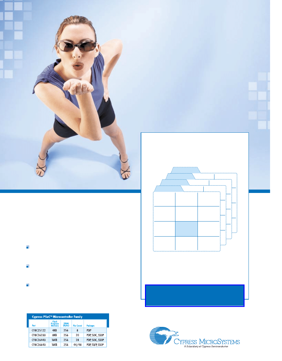
Use the Cypress PSoC
™
instead of an MCU for
more flexibility, fewer parts and lower cost.
The versatile PSoC
™
Programmable System-on-Chip
™
is
the world’s first mixed signal array that lets you custom
configure the exact functions you need. And it has an
on-chip controller to manage your application and run
the configuration process.
Graphically select, place, and interconnect
the peripherals you want and adapt the
architecture with PSoC Designer
™
software
Dynamically reconfigure a single PSoC
chip multiple times—changing functionality
on the fly in any application
Reduce BOM cost by reducing the number
of external components
MCU
later.
Cypress,
PSoC,
Programmable-System-on-Chip
and
PSoC
Designer
are
trademarks
of
Cypress
Semiconductor
Corporation.
©2002
Cypress
Semiconductor
Corporation.
All
other
Trademarks
are
the
property
of
their
respective
owners.
There are many more blocks to work with—
and thousands of configurations to choose from.
PSoC Designer
™
software is free for download, with
full-featured emulation hardware starting at $248.
Option #8926
8-bit PWM
Inverting Amplifier
IrDA
Transmitter
11-bit
Delta Sigma A/D
Band Pass Filter
Analog
Comparator
8-bit Counter
8-bit DAC
24-bit Timer
Low Pass Filter
Option #1530
Analog
Comparator
Instrumentation
Amplifier
12-bit
Incremental A/D
Notch Filter
16-bit CRC
Option #625
Analog
Comparator
16-bit PWM
Programmable
Gain Amplifier
Instrumentation
Amplifier
IrDA
Transmitter
11-bit
Delta Sigma A/D
8-bit DAC
12-bit
Incremental A/D
Band Pass Filter
8-bit Counter
Option #4237
CPU
Analog
Comparator
Your Customized Mixed Signal
platform in 60 minutes or less
Build your custom PSoC
™
with programmable analog
and digital functions from our extensive library.
To learn more about our innovative PSoC solutions
and to enter a drawing to win a PSoC Development
Digital Oscilloscopes
•
2 Channel Digital Oscilloscope
•
100 MSa/s
max single shot rate
•
32K samples per channel
•
Advanced Triggering
•
Only 9 oz and 6.3” x 3.75” x 1.25”
•
Small, Lightweight, and Portable
•
Parallel Port
interface to PC
•
Advanced Math options
•
FFT Spectrum Analyzer options
DSO-2102S
$525
DSO-2102M
$650
Each includes
Oscilloscope
,
Probes, Interface Cable, Power
Adapter, and software for
Win95/98, WinNT, Win2000
and DOS.
•
40 to 160 channels
•
up to 500 MSa/s
•
Variable Threshold
•
8 External Clocks
•
16 Level Triggering
•
up to 512K samples/ch
•
Optional Parallel Interface
•
Optional 100 MSa/s Pattern Generator
LA4240-32K (200MHz, 40CH)
$1350
LA4280-32K (200MHz, 80CH)
$2000
LA4540-128K (500MHz, 40CH)
$1900
LA4580-128K (500MHz, 80CH)
$2800
LA45160-128K (500MHz, 160CH)
$7000
Logic Analyzers
• 24 Channel Logic Analyzer
• 100MSa/S max sample rate
• Variable Threshold Voltage
• Large 128k Buffer
• Small, Lightweight and Portable
• Only 4 oz and 4.75” x 2.75” x 1”
• Parallel Port Interface to PC
• Trigger Out
• Windows 95/98 Software
LA2124-128K (100MSa/s, 24CH)
Clips, Wires, Interface Cable, AC
Adapter and Software
$800
All prices include Pods and Software
ne of our goals at
Circuit Cellar is to bring
you a variety of projects—from the serious and
complex to the lighthearted and fun. Each teaches
valuable techniques that you can use in your own
real-world applications. You can replicate the projects you read about, or
you can apply the techniques in a new way to suit your own needs. We
also look for fascinating emerging technologies that we think can bene-
fit you. This month, we’ve included a little bit of everything.
We start with a bit of levity. It’s almost summer, and that means bar-
becue. For an ordinary person, that might mean rolling out the gas grill
from the garage to grill hot dogs and hamburgers. But, for an engineer,
it means a project. John Moyer used his engineering prowess to design
a sophisticated grill that’s sure to make him the envy of every other guy
in the neighborhood (p. 28). Rather than use the average Weber or
George Foreman grill, he opted for a unique ceramic cooker. As any
die-hard barbecue fan knows, slow cooking meat to get that perfect
barbecue flavor takes days. Most people just don’t have that kind of
time to tend the fire. So, John designed an automatic temperature con-
troller to tend the fire for him. With a microprocessor, thermocouple,
and some other parts, he’s now able to prepare beef brisket the way it
should be done, and not get fired for leaving work to check the meat.
Why be content with a purchase when you know you can make it
better? And, how about testing that product to see what you’ve actually
bought? When you look at factory specs, you might wonder how accu-
rate they are. Did the manufacturer fudge the numbers at all? Are they
attainable only under a precise set of optimum circumstances? With an
accelerometer from Analog Devices and a PIC microcontroller, Ross
Tsukashima set out to test the limits of his new car (p. 24). As is often the
case, the testing equipment available off the shelf wasn’t an option, so he
built his own G-force meter specially designed to meet his goals. You’ll
want to read on to find out if his New Beetle lives up to its reputation.
We think you’ll be equally interested in reading about Zoltan
Molnar’s Bluetooth application (p. 44). With the trend toward wireless
firmly in place, Bluetooth is gaining popularity. Zoltan focused on a spe-
cific mode of connectivity—using only HCI interfaces. He created
Blueport, an interface that enables you to connect simple embedded
systems to the complex Bluetooth protocol stack. Despite having limited
resources and no external RAM, you can achieve this type of wireless
connectivity with a creative solution. That’s great news for engineers
working primarily with 8-bit microcontrollers.
4
Issue 154 May 2003
www.circuitcellar.com
CIRCUIT CELLAR
®
EDITORIAL DIRECTOR/FOUNDER
Steve Ciarcia
MANAGING EDITOR
Jennifer Huber
TECHNICAL EDITOR
C.J. Abate
WEST COAST EDITOR
Tom Cantrell
CONTRIBUTING EDITORS
Ingo Cyliax
Fred Eady
George Martin
George Novacek
Jeff Bachiochi
NEW PRODUCTS EDITOR
John Gorsky
PROJECT EDITORS
Steve Bedford
Ken Davidson
David Tweed
ADVERTISING
PUBLISHER
Dan Rodrigues
E-mail: dan@circuitcellar.com
ASSOCIATE PUBLISHER / DIR. OF SALES
Sean Donnelly
Fax: (860) 871-0411
(860) 872-3064
E-mail: sean@circuitcellar.com
Cell phone: (860) 930-4326
ADVERTISING COORDINATOR
Valerie Luster
Fax: (860) 871-0411
(860) 875-2199
E-mail: val.luster@circuitcellar.com
ADVERTISING ASSISTANT
Deborah Lavoie
Fax: (860) 871-0411
(860) 875-2199
E-mail: debbie.lavoie@circuitcellar.com
CONTACTING CIRCUIT CELLAR
SUBSCRIPTIONS:
INFORMATION: www.circuitcellar.com or subscribe@circuitcellar.com
To Subscribe: (800) 269-6301, www.circuitcellar.com/subscribe.htm, or
subscribe@circuitcellar.com
PROBLEMS: subscribe@circuitcellar.com
GENERAL INFORMATION:
TELEPHONE: (860) 875-2199 Fax: (860) 871-0411
INTERNET: info@circuitcellar.com, editor@circuitcellar.com, or www.circuitcellar.com
EDITORIAL OFFICES: Editor, Circuit Cellar, 4 Park St., Vernon, CT 06066
NEW PRODUCTS: New Products, Circuit Cellar, 4 Park St., Vernon, CT 06066
newproducts@circuitcellar.com
AUTHOR CONTACT:
E-MAIL: Author addresses (when available) are included at the end of each article.
CIRCUIT CELLAR®, THE MAGAZINE FOR COMPUTER APPLICATIONS (ISSN 1528-0608) and Circuit Cellar Online are pub-
lished monthly by Circuit Cellar Incorporated, 4 Park Street, Suite 20, Vernon, CT 06066 (860) 875-2751. Periodical rates paid at
Vernon, CT and additional offices.
One-year (12 issues) subscription rate USA and possessions $21.95, Canada/Mexico
$31.95, all other countries $49.95. Two-year (24 issues) subscription rate USA and possessions $39.95, Canada/Mexico
$55, all other countries $85.
All subscription orders payable in U.S. funds only via VISA, MasterCard, international postal money
order, or check drawn on U.S. bank.
Direct subscription orders and subscription-related questions to Circuit Cellar Subscriptions, P.O. Box 5650, Hanover, NH
03755-5650 or call (800) 269-6301.
Postmaster:
Send address changes to Circuit Cellar, Circulation Dept., P.O. Box 5650, Hanover, NH 03755-5650.
For information on authorized reprints of articles,
contact Jeannette Ciarcia (860) 875-2199 or e-mail jciarcia@circuitcellar.com.
Circuit Cellar® makes no warranties and assumes no responsibility or liability of any kind for errors in these programs or schematics or for the
consequences of any such errors. Furthermore, because of possible variation in the quality and condition of materials and workmanship of read-
er-assembled projects, Circuit Cellar® disclaims any responsibility for the safe and proper function of reader-assembled projects based upon or
from plans, descriptions, or information published by Circuit Cellar®.
The information provided by Circuit Cellar® is for educational purposes. Circuit Cellar® makes no claims or warrants that readers have a right to
build things based upon these ideas under patent or other relevant intellectual property law in their jurisdiction, or that readers have a right to
construct or operate any of the devices described herein under the relevant patent or other intellectual property law of the reader’s jurisdiction.
The reader assumes any risk of infringement liability for constructing or operating such devices.
Entire contents copyright © 2001 by Circuit Cellar Incorporated. All rights reserved. Circuit Cellar and Circuit Cellar INK are registered trademarks
of Circuit Cellar Inc. Reproduction of this publication in whole or in part without written consent from Circuit Cellar Inc. is prohibited.
CHIEF FINANCIAL OFFICER
Jeannette Ciarcia
CUSTOMER SERVICE
Elaine Johnston
ACCOUNTANT
Jeff Yanco
ART DIRECTOR
KC Prescott
GRAPHIC DESIGNER
Mary Turek
STAFF ENGINEER
John Gorsky
QUIZ COORDINATOR
David Tweed
TASK
MANAGER
Cover photograph Chris Rakoczy—Rakoczy Photography
PRINTED IN THE UNITED STATES
o
Variety is the Spice of Life
jennifer.huber@circuitcellar.com
Con
fide
ntia
l
CANbus
Starter Packs
available for almost
any board format: PCI, ISA, PCMCIA, PC104,
VME, cPCI, etc. with software for most
OS’s inc. all Win, Linux, QNIX, etc.
CAN/Ethernet bridges, industrial
computing and automation solutions
Industry leaders worldwide trust and
specify Janz AG’s ISO9000 systems.
www.saelig.com • saelig@aol.com
check out what’s new at www.saelig.com!
by
Janz
for
all
computers
ALSO:
SMD PROTOTYPING ADAPTER PCBs
S C A L A B L E L E D D I S P L A Y P A N E L S
TEMPERATURE-HUMIDITY MONITORS
T H E R M O C O U P L E P . C . A D A P T E R S
ENVIRONMENTAL MON. SYSTEMS
WILKE BASIC TIGER CONTROLLERS
Saelig Co. brings to USA unique, easy-to-use control and
instrumentation products from overseas. Customers inc:
Intel, Compaq, Philips, NEC, Kodak, Nokia, US Military,
Microsoft, Dell, Xerox, Universities, T.I., Harris, Sony,
J&J, Thomson, Sandisk, General Dynamics, H-P, etc.
DrDAQ
Educational datalogger
ADC-212/100
12-bit 100MHz PC scope
Euroquartz
crystals & oscillators
TRAKIT
manufacturing software
K3 / K2
self-powered isol/non-isol RS232-485
USB-485i
isolated USB<>RS485
PCI93LV/C
PCIbus I2C adapter
ANT8
USB logic analyzer
BIT2000
simple factory control
US232
USB-serial port adapter
TDS2020F
Forth-based datalogger/controller
USB TRACKER 110
USB bus analyzer
FT232BM / FT245BM
single ic USB solution - no programming!
JANZ - CANbus
CAN interface cards - all formats
DS2200C
USB PC scope
Turns your PC into a high-
speed scope. Sampling
rates up to 100MS/s for sin-
gle shot signals (and up to
5GS/s for repetitive signals)
with 12-bit resolution. With
FREE software, your PC
becomes a powerful 2-chan-
nel scope and spectrum
analyzer. - $1090
DrDAQ plugs into a PC
for datalogging at
school, college, indus-
try. Built-in sensors for
light, sound, temp. or
add pH sensor and run
one of the many sug-
gested science experi-
ments!
- only $99!
US232 is a 6ft USB-RS232
self-powered converter
cable which instantly and
reliably solves the problem
of laptops with no serial
ports, or legacy RS232
devices that need to be
updated to USB IN ONLY 5
MINUTES!
Buy in bulk to
update your products - $39!
"After looking at a number of packages
both large and small we have found
TRAKIT
TM
to be the most cost effective
solution for inventory management in the
manufacturing environment available for
the small to medium size company. It
contains most of the commonly used
features of the larger programs as well as
maintaining the user ease of the smaller
programs. Some of the more advanced
features of Trakit are more successfully
implemented than packages costing
many times more. Better and easier to
use than P&V" (S.P. Ltd)
TRAKIT
manufacturing
- Inventory Management
- Bills of Materials
- Build Schedule
- Sales Orders
- Instant Builds
- Purchase Ordering
- Request for Quote
- Reminders
- Reports
K2
9p-9p self-powered RS-422/485 converter
K3
9p-9p isolated RS-422/485 converter
K3-232
9p-9p isolated RS232 converter
K232-ISOL
25p -25p RS232
K422-ISOL
25p -25p RS422
K485-ISOL
25p -25p RS485
KD485-STD
DINrail-mount
RS-232/485/20mA isolators
KD485-PROG
DINrail-mount
RS-232/485/20mA isolators
C-programmable for protocol/MODbus
conversion. Program to convert custom needs.
USB-485i offers self-
powered USB to RS485
conversion with optical
isolation to 1kV. Baud
rates 184bps - 3Mbps.
Link-selectable half-duplex
mode enables the 485
transmit-buffer when data
ready. Three-point isolated
serial communciations.
200 kS/s 12-bit dual-channel USB scope adapter for
PC. Unique software looks like a “Digital Scope”
right on your PC screen!
Built-in squarewave
generator. Weighs <8oz.
Only $189!! For details:
www.usb-instruments.com
USB protocol analyzer displays USB packets sent,
decodes descriptors, detects errors in peripherals or
drivers and measures their performance.
Ideal for anyone developing
USB peripherals,
embedded soft-
ware or drivers.
Software is easy
to use - learn all
about USB. $799!
Make PCs talk I2C easily with this industry-standard
card, available in 2 - 6V bus version for low-volt I2C
systems. Optional WINI2C/PCI software gives you a
windows-interface to develop
and debug I2C bus systems.
Monitor software lets you
transparently monitor I2C bus
activity . Other bus-versions
available too! Please call!
Build a custom PCMCIA or CF
card datalogger or controller
- quickly!
Wizard high-level
software completes your
project in hours not weeks.
Store GPS or CANbus data.
TDS2020F is the low-power
controller of choice for sure
LONGEVITY - this one won’t
disappear like so many other
obsolete boards. Ask us why!
Join all the industry leaders
who are using this easy-use
USB ic. Single chip USB-
232 solution comes with all
Windows/Mac/Linux drivers.
UART ASIC-based so no
software development is
needed! No knowledge of
USB needed either! Byte-
wide version FT245BM too!
Euroquartz is one Europe’s largest manufacturers and
supplier of quartz crystals, oscillators, filters and
frequency-related products. They design & manufacture
a comprehensive range of frequency-related components
including custom-made filters, high
reliability oscillators for defence
applications and radiation tolerant
oscillators for high-altitude apps.
EQ-HM oscillators reduce EMI using
Spread Spectrum Technology
to slowly shift center frequency.
Easily construct small control systems communicating
through Intranet/Internet. BIT2000 is the ideal solution
for process control, building
monitoring, data logging,
alarm systems and other
industrial uses. BIT2000
can communicate with
many types of equipment
through the fast multidrop
RS485 based bus and a
standard RS232 serial port.
At last!
This tiny pocketable USB-based and USB-
powered device is the answer to your need for an eco-
nomical logic analyzer that you can take anywhere.
About the size of a small matchbox, ANT8 can sample
eight channels at up to 500 million samples-per-sec.
Ant8 offers simple or complex
triggering, upgradeable soft-
ware. View the captured eight
digital channel traces on your
PC. Save or print screens for
reference or notes! $199!
6
Issue 154 May 2003
CIRCUIT CELLAR
®
www.circuitcellar.com
DTMF-Controlled Remote Switching System
Bluetooth Interface for Embedded Systems
Updating the Home Control System
Part 3: The Complete Upgrade Solution
I
New ICE Age
MPLAB ICE 2000 Replaces PICMASTER
I
Making Sense of the Gerber File Format
I
COLUMNS
ISSUE
Advertiser’s Index
June Preview
Priority Interrupt
Steve Ciarcia
4
8
11
94
96
154
12
24
36
28
FEA
TURES
Contest-Related Article
62
80
44
74
54
70
Check out AVR today at www.atmel.com/ad/fastavr
Introducing the Atmel AVR
®
. An 8-bit MCU that
can help you beat the pants off your competition.
AVR is a RISC CPU running single cycle instructions.
With its rich, CISC-like instruction set and 32 working registers,
it has very high code density and searingly fast execution–up to
16 MIPS. That’s 12 times faster than conventional 8-bit micros.
We like to think of it as 16-bit performance at an 8-bit price.
With up to 128 Kbytes of programmable Flash and EEPROM,
AVR is not only up to 12 times faster than the MCU you’re using
now. It’s probably 12 times smarter, too.
And when you consider that it can help slash months off your
development schedule and save thousands of dollars in project
cost, it could make you look pretty smart, too.
AVR comes in a wide range of package and performance
options covering a huge number of consumer and industrial
applications. And it’s supported by some of the best development
tools in the business.
So get your project started right. Check out AVR today at
www.atmel.com/ad/fastavr. Then register to qualify for your free
evaluation kit and bumper sticker. And get ready to take on the world.
Our AVR microcontroller is
probably 12 times faster than
the one you’re using now.
(It’s also smarter.)
AVR 8-bit RISC Microcontrollers
© 2002 Atmel Corporation. Atmel and the Atmel logo are registered trademarks of Atmel Corporation.
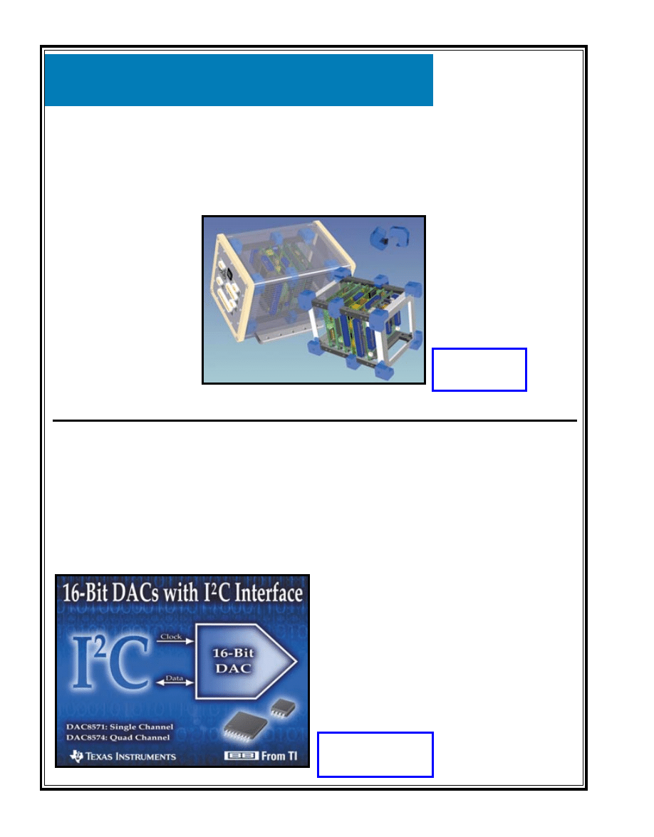
SHOCK AND VIBRATION ISOLATORS
The PC/104 Shock Rocks line of shock and vibration
mitigation products is designed to enhance the durabil-
ity of embedded PC/104 computer systems that under-
go mechanical stress.
Made of 59 durometer Silastic(r) silicone rubber
material, these compact
shock isolators successfully
reduce G-force frequencies on
three axes by up to a factor of
10, making them well suited
for a wide variety of mobile,
airborne, shipboard, space,
and other demanding applica-
tions common to the aero-
space, defense, medical, and
transportation fields.
Designed to attach to the
outside perimeter of a 4
″
× 4
″
PC/104 railed card cage,
Shock Rocks isolate all
points of contact between a
NEWS
8
Issue 154 May 2003
CIRCUIT CELLAR
®
www.circuitcellar.com
NEW PRODUCT
Edited by John Gorsky
removable aluminum card cage and its surrounding
enclosure. Mounting PC/104 modules within a card cage
in this way eliminates the need for traditional PCB
standoffs/spacers; it provides a much simpler board
removal method over PC/104 containers using compres-
sion-mounted rubber rails.
Depending on the size of
the card cage, between eight
and 12 Shock Rocks are typi-
cally attached. Packaging
PC/104 systems in such a
configuration can provide a
NEMA 4× environmental
protection together with sig-
nificant shock/vibration tol-
erance.
The Shock Rocks cost $10.
Parvus Corp.
(801) 483-1533
www.parvus.com
out additional glue logic, enabling the simultaneous
update of up to 64 channels.
The DAC8571 and DAC8574 also support an I
2
C
high-speed mode, allowing rapid 188-ksps DAC
update rates at 3.4-MHz clock speed. The DAC8571
consumes only 170 µA of the supply current at 5 V,
and the DAC8574 consumes 950 µA of current at
5 V. A per-channel, power-down mode reduces the
maximum supply current to 1 µW. A power-on reset
circuit ensures that the DACs power up at 0 V and
remain there until a valid write occurs. Both convert-
ers operate on a single 2.7- to 5.5-V supply.
Both devices feature rail-to-rail outputs, 10-µs set-
tling, true 16-bit monotonic performance, a 94-dB sig-
nal-to-noise ratio, and less than 1-mV offset drift over
the –40° to 105°C temperature range. The DAC8571
offers less than 1-mV offset error at 25°C. An external
reference voltage is required to set the output voltage
range of both DACs.
The DAC8571 comes in an MSOP-8 package and
costs $2.83 in 1000-piece quantities. The DAC8574
comes in a TSSOP-16 package and costs $9.75 in 1000-
piece quantities.
Texas Instruments, Inc.
(800) 336-5236
www.ti.com
LOW-POWER, 16-BIT DACs WITH I
2
C
The DAC8571 and DAC8574 are the industry’s first
low-power, 16-bit DACs with an I
2
C interface. These
devices are ideal for portable systems, including industri-
al process control, instrumentation, and data acquisition.
The DAC8571 (single channel) and DAC8574 (quad
channel) use an I
2
C-compatible two-wire serial interface
to support high-precision, high-channel-count data
acquisition systems. With their broadcast feature,
multiple devices can work on the same I
2
C bus with-
www.circuitcellar.com
CIRCUIT CELLAR
®
Issue 154 May 2003
9
NEWS
NEW PRODUCT
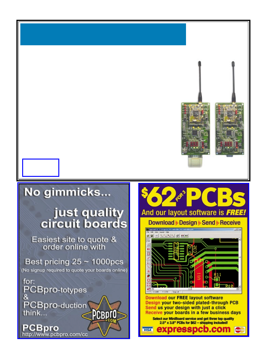
LOW-COST TRANSCEIVER DEVELOPMENT PLATFORM
The XE1202SK starter kit is a new low-cost development platform that
enables the demonstration of two-way communication between two radio
boards. The kit can be used to facilitate “out of the box” range-testing
demonstrations. A PC graphical user interface enables a simple but practical
development environment for evaluation of the RF transceiver. The
XE1202SK performs basic functions with a ping-pong demo as the default
configuration, plus features such as XE1202 register configuration and trans-
mission/reception of a serial data stream between two units.
The kit includes two main boards, RF modules, instructions, and software.
The tool kit enables RF evaluation of the XE1202SK basic functions of config-
uration in Transmitter, Receiver, or Sleep mode, frequency deviation selec-
tion, filter bandwidth, and output power management.
The XE1202SK enables the demonstration of two-way communication
between two radio boards and practical demonstration with a ping-pong
demo. You can also use it to perform range and site survey testing, and evalu-
ate the RF transceiver through a user-friendly PC GUI interface. The demo
can be customized with user settings. There are three frequencies and four
output powers to choose from.
The starter kit costs $250.
10
Issue 154 May 2003
CIRCUIT CELLAR
®
www.circuitcellar.com
NEWS
NEW PRODUCT
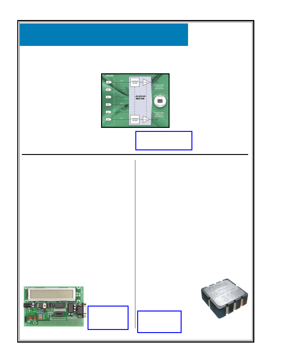
SIX-CHANNEL VIDEO RECONSTRUCTION FILTER
The MAX7440, MAX7441, and MAX7442 are the
industry’s first six-channel video reconstruction filters.
These devices are ideal for antialias-
ing and digital-to-analog reconstruc-
tion video applications such as set-
top boxes, DVD players, hard-disk
recorders, and personal video
recorders. Each channel of the
device combines a continuous-time
low-pass filter with high-frequency
boost options and a unity-gain
amplifier. High performance and
integration make these devices ideal
for European STBs using SCART
connectors.
The MAX7440, MAX7441, and MAX7442 support
composite video (CVBS), S-Video (Y/C), and component
(RGB or Y Pr Pb) video signals for both NTSC and PAL.
PIC EXPERIMENTER BOARD
The LAB-X4 experimenter board is designed to
accommodate both the 8-pin PIC12F675 and its 14-pin
counterpart, the PIC16F676. The experimenter board
provides all the circuitry required by the MCU to oper-
ate: a 5-V power supply and reset circuit, an RS-232 seri-
al port, a 2 × 20 LCD module with a serial controller,
and basic analog and digital I/O.
With the assembled LAB-X4, you can develop a vari-
ety of applications for the PIC12F675 and PIC16F676.
For example, the LCD can display the time of day. You
can use the LAB-X4 to make a robot brain that controls
RC servos. The RS-232 serial port can be used for two-
way communication with your computer.
The LAB-X4 can run programs written in assembler,
C, PicBasic, or PicBasic Pro. The included samples are
for PicBasic and PicBasic Pro. There are also precompiled
hex files that you can use if you don’t have a compiler.
The experimenter board can be connected directly to
a device programmer for in-circuit serial programming.
It can be erased and reprogrammed in seconds, allowing
you to quickly test changes to your program code.
The LAB-X4 is available preassembled for $125 or as
a bare PCB for just $25. Both versions come with full
documentation,
including schemat-
ics, a parts list, and
sample programs.
MicroEngineering
Labs, Inc.
(719) 520-5323
www.melabs.com
FULLY INTEGRATED MEMS ACCELEROMETER
The ADXL311 is a fully integrated, low-power, low-g
MEMS accelerometer.
The ADXL311 uses the reliable iMEMS surface
micromachining technology with proven circuit, sensor,
and process reliability performance of better than 1 FIT
(failure in time). The device, along with future low-cost
iMEMS accelerometers, will play a significant role in
enabling tilt- and motion-sensing features in many cost-
sensitive applications.
The ADXL311 is a dual-axis,
±
2-g (at full-scale)
accelerometer with analog outputs that can measure
both dynamic acceleration (vibration) and static acceler-
ation (gravity). The accelerometer integrates moving
microscopic silicon parts and sophisticated signal condi-
tioning to produce a complete two-axis accelerometer
on a single monolithic IC. It features low-power require-
ments—200 µA per axis at 3-V operation. The typical
noise floor is 300 µg per root hertz at 3-V operation and
allows signals below 5 mg to be resolved for bandwidths
below 60 Hz. The ADXL311 is packaged in a 5 mm × 5
mm × 2 mm eight-lead her-
metic LCC package and pro-
vides an accurate low-power
method of measuring tilt,
shock, and vibration.
The ADXL311 is priced at
$2.50 in quantities greater
than 10,000 units.
Analog Devices, Inc.
(781) 937-1428
www.analog.com
The filter achieves 40 dB of stopband rejection at 27 MHz
with a maximum flat passband of only
±
0.5-dB ripple.
High-frequency boost circuitry pro-
vides picture sharpness adjustment
without degradation in the stopband
attenuation.
These devices save board space
and insertion costs by replacing up
to 30 discrete components. The
MAX7440, MAX7441, and MAX7442
are packaged in a 14-pin SO in the
–40 to 85° C extended temperature
range. The ICs start at $1.21 in
1000-piece quantities.
www.circuitcellar.com
CIRCUIT CELLAR
®
Issue 154 May 2003
11
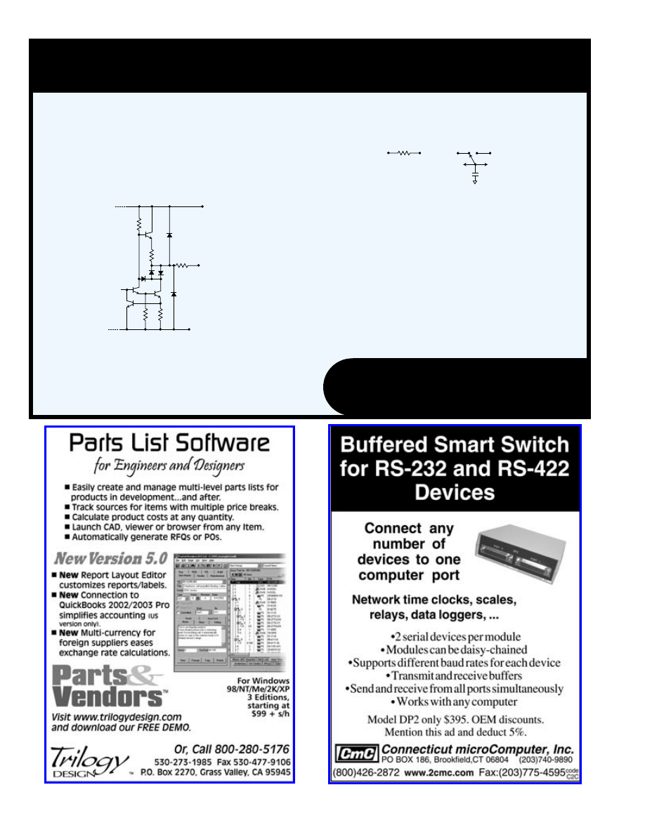
Problem 3
—
Are the two circuits below equivalent?
Explain.
Contributed by Dave Tweed
Problem 4
—
Some filters have flat passbands and roll
off smoothly in their transition regions. Other filters accept
a small amount of ripple in their passbands in order to
achieve steeper transitions. What is the implication in the
time domain of these ripples?
Contributed by Dave Tweed
What’s your EQ?
—
The answers are posted at
www.circuitcellar.com/eq.htm
You may contact the quizmasters at eq@circuitcellar.com
CIRCUIT CELLAR
—
What is the func-
Test Y
Your E
EQ
Problem 1
—
The output stage of a generic ’1488 RS-
232 driver is shown below. The input stage has an out-
put impedance of roughly 10 K
Ω
and functions so that
Q1 is basically either cut off or saturated. One of the
functions of an RS-232 driver is to limit the drive current
to approximately 10 mA. Does this circuit accomplish
that? If so, show how it does it for both output states.
Contributed by Dave Tweed
Problem 2
—
What is the function of D3 in the circuit
in question 1?
Contributed by Dave Tweed
Edited by Dave Tweed
Q2
D4
70
6200
300
Output
+V
D5
D1
Q1
Q3
D3
D2
70
Q4
3700
From input
stage
V–
V1
R
C
F
V2
a)
b)

12
Issue 154 May 2003
CIRCUIT CELLAR
®
www.circuitcellar.com
remember the
first time someone
asked me to design a
cable tester. I was a
bright-eyed co-op student on a sum-
mer work term. My boss asked me to
design a cable tester to find the faults
in the printer cables we were manu-
facturing. To test the cables, we’d nor-
mally plug one end into the printer,
the other end into a computer, and
then print. Of course, if the cables
were miswired, tracing the problem
required a manual pin-to-pin investi-
gation with an ohmmeter. Verifying
25 to 36 connections by hand turned
out to be a tad time consuming, to say
the least. To do the job, I was given an
Apple II computer (this was some
time ago), a Basic compiler, and a
handful of decoders and multiplexers.
After thinking about the problem, I
got busy and came up with a design
that accurately pinpointed the cable
wiring problems.
The reason I mention that incident
is because today, almost 25 years later,
many of the same problems still exist.
There aren’t any general-purpose, inex-
pensive methods for testing cables.
Technology has made some advances,
so we now have more computing
power than the Apple II available in
an 18-pin DIP package. Compilers are
also much better. After seeing my
company’s production personnel strug-
gle to test a multitude of cables, I
experienced déjà vu. What they really
needed was a modern version of the
tester I had designed in my university
days. Of course, this updated design
would be based on a PIC processor and
use a modern freeware language called
JAL (see Photo 1). [1] At the time, I
wanted to minimize development
costs, so buying a PIC C compiler was
out of the question. Take a look at the
sidebar for a brief description of JAL.
DESIGN ON A SHOESTRING
To minimize hardware complexity, I
initially looked at the PICs with the
highest number of input/output pins.
Unfortunately, our largest cable had
31 pins, requiring a PIC with at least
64 pins (including power and ground).
I could have used a PIC17C766 with
84 pins and 66 I/O ports, but it’s quite
pricey—almost five times the cost of
the part I chose. Then there was the
problem of exposing the PIC’s pins to
static discharges. In addition, the
cables might have been wired so badly
that outputs were driving other out-
puts. Consequently, all of the I/O con-
nections were first buffered, so that in
the case of any damage, the produc-
General-Purpose Cable
Tester
l
Michael built his first
cable tester with an
Apple II, Basic compil-
er, and several
decoders and multi-
plexers. Twenty-five
years later, it’s still
hard to find cost-effec-
tive, general-purpose
cable testers. So he’s
at it again, but this
time he’s armed with
a PIC micro and JAL.
Michael Griebling
FEATURE
ARTICLE
Stand-Alone or with a GUI
Command
PIC Reply
Function
Pxx yy<CR>
OK<CR>
Program EEPROM location xx (hex) with data yy (decimal) and reply
NPR<CR>
Programming EEPROM failed
NAK<CR>
Illegal EEPROM address, invalid pin number, or other errors
Tyy<CR>
Vzzzzzzzz<CR> Test pin yy (decimal 1-32) and return result vector zzzz (hex)
NAK<CR>
Communication error or illegal pin number
Table 1—
Take a look at the host commands and the PIC reply. Sending a host command
P3F 20
programs EEP-
ROM location 0x3F with 0x20. The host command
T10
causes pin 10 to be pulsed low and the resultant vector
reply from the PIC should be VFFFFFDFF.
www.circuitcellar.com
CIRCUIT CELLAR
®
Issue 154 May 2003
13
GOD’S IN THE DETAILS
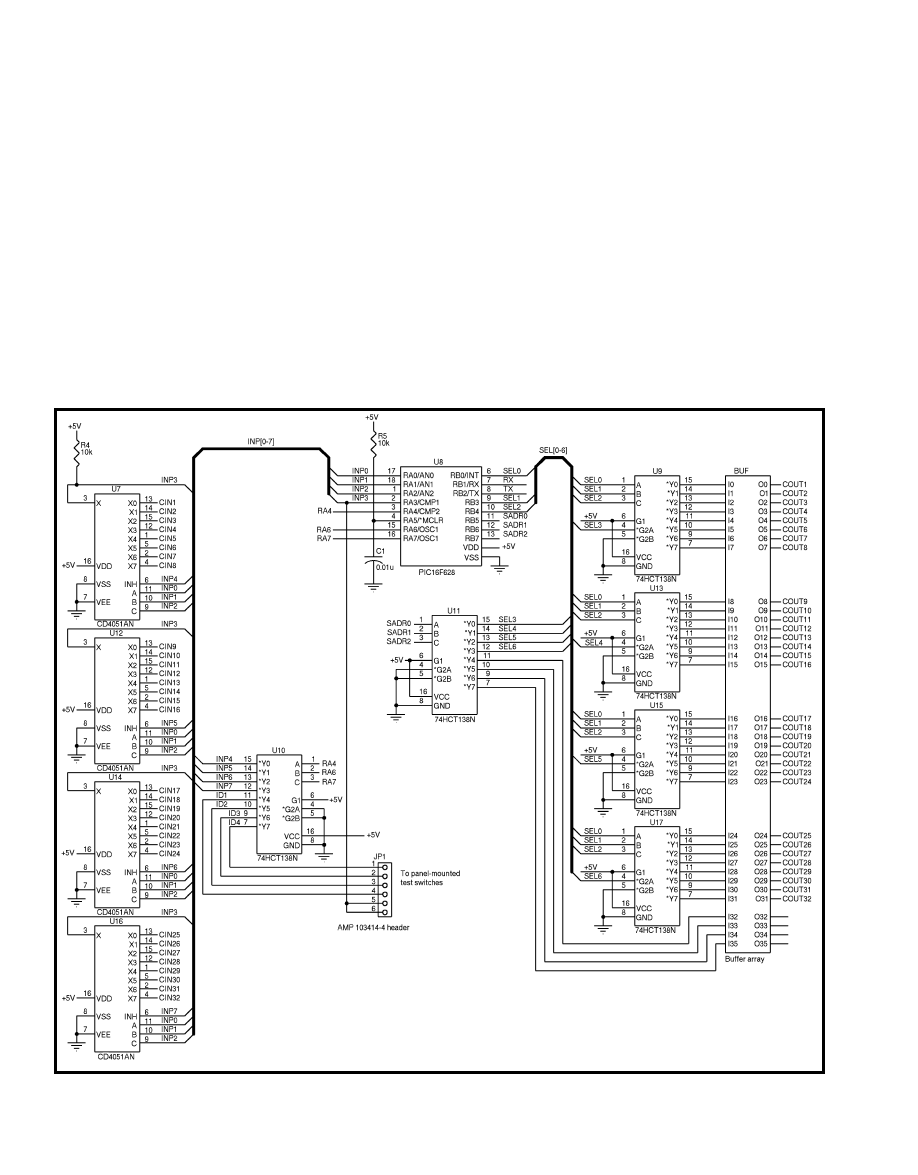
Figure 2 shows the detailed
schematic of the PIC16F628
processor and surrounding cir-
cuitry. [2] The cable pin driver
signals are generated by five
74HCT138 decoders based on
a 6-bit address supplied by the
PIC. The lower three bits
select one of eight outputs
from U9, U13, U15, and U17,
which are applied to the pin
driver circuitry (Figure 3).
The upper three bits select
one of the four decoders and
also generate four status LED
driver signals.
The buffer array (7407)
drives the pin LEDs and provides the
open-collector isolation for the 32 cable-
drive pins. The buffers are arranged in
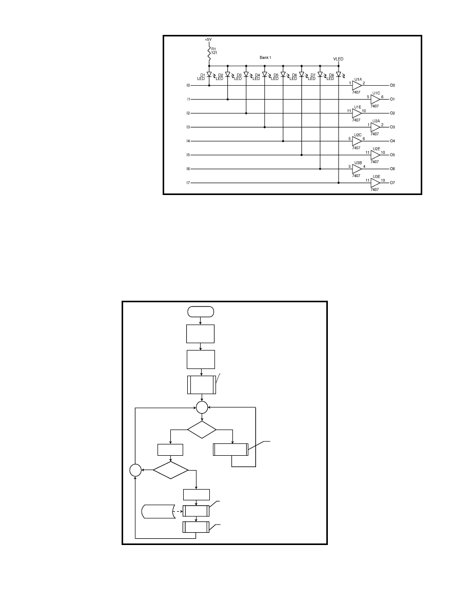
four banks of eight bits. Figure 3 shows
the detail of a single bank. Eight LEDs
monitor the pin drive status so that
when a particular pin is being driven
(grounded), the corresponding LED
illuminates. Note that a single resistor
suffices for all 32 LEDs, because only
one output pin is driven at a time. An
open-collector buffer is located after
the LED so cable short circuits don’t
cause multiple LEDs to illuminate.
At the receiving end of the cable, U7,
U12, U14, and U16 form a 32-input
multiplexer that selects one of the cable
inputs at a time (see Figure 2). The PIC
selects a particular input using a 6-bit
address, where the lower three bits
tion staff could easily replace a cheap,
socketed driver and not the more
expensive PIC, which would then
need to be reprogrammed and retested.
A second requirement was to give
the operator a visible way to know
that the test is in progress and which
wiring connections are incorrect when
operating in Stand-Alone mode. My
solution was to equip the cable tester
with a series of LEDs—one for each
pin—that would show when a particu-
lar pin was driven and could double as
a simple fault display.
When operating independently, up
to four different cables can be tested,
one at a time, based on vectors stored
in the internal EEPROM. The individ-
ual tests are initiated when one of
four push buttons is pressed.
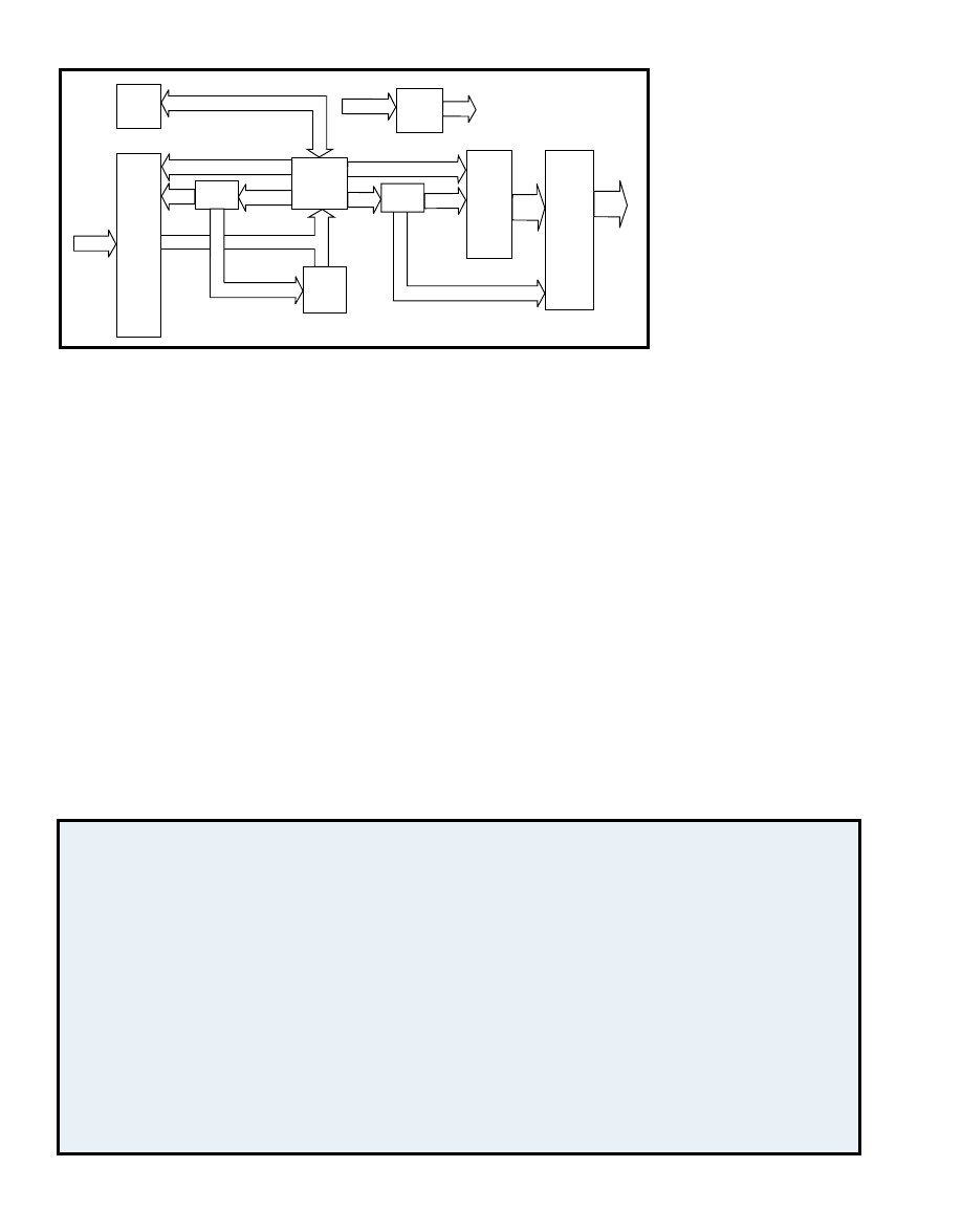
Figure 1 illustrates the basic hard-
ware components used in the cable
tester. The central PIC processor drives
a five-to-32 decoder that strobes each
cable pin sequentially. A second three-
to-eight decoder is used to either select
the pin output strobes or drive four sta-
tus LEDs. The cable-drive signals are
buffered with open-collector, high-volt-
age drivers, which prevent cable short
circuits from damaging any pin drivers.
On the receiving-cable end, a 32-to-one
analog multiplexer is controlled by the
PIC to select one cable pin at a time. A
second three-to-eight decoder selects
either the analog multiplexer or one of
the four test-select switches. Remote
mode is also available when a PC-based
program is connected to the cable tester
with a standard RS-232 serial cable.
A BRIEF HISTORY OF JAL
Developed by Wouter van Ooijen, just another lan-
guage (JAL) was patterned after Ada, the military stan-
dard language. But if you’re familiar with Pascal, you
should have no trouble understanding JAL. You’ll find
the software free of charge at www.voti.nl/jal. The
author would like to be notified via e-mail, postcard, or
letter for any significant use.
When I spoke to Wouter, he said he created JAL
because he did not like any of the PIC16F84’s low-cost,
high-level languages. Also, he thought implementing a
high-level language seemed like a worthwhile project.
Since its creation in 1999, a small but devoted group
of embedded programmers has been using JAL. The
group meets via a mailing list located at groups.
yahoo.com/group/jallist/.
In its present incarnation, JAL supports Microchip PIC
(e.g., PIC16C84, ’16F84, ’12C508, ’12C509, and ’16F877)
and Ubicom SX (e.g., SX18 and SX28) microcontrollers as
targets. It provides conditions, statements, expressions,
subprograms, and variables. Available data types include
bits, bytes, and universal integers. Structured data types
such as arrays and records are not yet available. A pro-
gram can be split into separate files that are all included
in the main source code file; however, separate compila-
tion isn’t supported so that global optimizations can be
performed more easily.
A separate Windows IDE called JalCC is available at
oase.uci.kun.nl/~mientki/PIC/JALcc.htm. It has been
adapted by Stef Mientki from the BricxCC IDE. Stef and
others are actively supporting it.
RS-232 IF
32-to-1
MUX
C
IN
1-32
3-to-8
Decode
Test
switches
PIC16F628
RX/TX
A0-A2 (INP0-2)
INP4-7
A4, A6, A7
A3 (INP3)
ID1-4
5-V
Switcher
9–32 V In
5 V
ID1-4
B0, B3, B4
3-to-8
Decode
B6–B7
SEL3-6
5-to-32
Decode
DRV
1-32
C
OUT
1-32
OC Buffers
and
LEDs
SEL0-3
ID1-4
Figure 1—
Look at the PIC16F628 surrounded by address decoders and input multiplexers. A 5-V switcher powers the circuitry,
and an RS-232 interface connects to an external PC to download cable definitions and/or operate as a slave tester.
14
Issue 154 May 2003
CIRCUIT CELLAR
®
www.circuitcellar.com
select one of eight inputs and the upper
three bits select a particular multiplexer
via U10, a three-to-eight decoder.
In addition to sampling the cable
inputs, this circuitry also provides puls-
es to the four test-select push buttons.
One common end of each push button
is tied to the INP3 or multiplexer input
to the PIC. Thus, by sequentially
selecting outputs Y4 through Y7 of
U10 and monitoring the INP3 input, a
simple keyboard-style scanning func-
tion is provided. R4 provides a needed
pull-up for the INP3 multiplexer input;
however, at 10 k
Ω
, it tends to slow
down the cable tester when cables
with a lot of capacitance are tested.
The RS-232 interface is a straightfor-
ward implementation that is driven by
the PIC’s serial interface pins. The
interface operates at 9600 bps; it’s used
to download new cable vectors to the
EEPROM for stand-alone operation, or
you can use it to remotely control
cable testing when implemented with
the PC-based software. You may down-
load the RS-232 schematic from the
Circuit Cellar
ftp site.
The 5-V power supply is a simple
switcher-based design with an
LM2670 adjustable Buck mode regula-
tor. [3] You may download a schemat-
ic diagram of the 5-V power supply
from the Circuit Cellar ftp site.
I chose an LM2670 3-A regulator
instead of a linear regulator, because
it’s a stock item used in my company’s
products. The power consumption of
the cable tester is negligible, so the
existing part is admittedly overkill.
Switching regulators are much more
efficient than linear regulators. This
may be a consideration if the cable
tester were to be battery powered.
ROOM FOR GROWTH
With some minor software and hard-
ware changes, it should be possible to
easily expand the size of cables that
can be tested up to 60 pins. The Y4-
to-Y7 outputs of U10 would each drive
an additional CD4051 analog multi-
plexer, and the upper four pins would
serve as the manual-test push button
Figure 2—
The Microchip PIC16F628 microcontroller drives 74HCT138 address decoders that are buffered by open-collector drivers. At the input CD4051 MUXes multiplex the
cable inputs to a single input pin, INP3.

EFFORT…BIG
PRIZES!
Innovate with the HC08 from Motorola
Innovate with the HC08 from Motorola
These products incorporate SuperFlash
®
technology licensed from SST. Motorola and the stylized M Logo are registered in the U.S.
Patent and Trademark Office. All other product or service names are the property of their respective owners. © Motorola, Inc. 2002
68HC908QT4 Demonstration Kit
Flash Innovation 2003 Design Contest
Enter our Flash Innovation
2003 Design Contest
involving our new HC08
Q-Family. You may be
eligible to win a 60” thin
plasma screen HDTV
or one of several other
exciting prizes. We are
offering prizes valued
together at more
than $30,000.
Innovate with the HC08!
Motorola’s HC08 Q-Family
of 8-bit microcontrollers
is available in small
8- and 16-pin packaging.
With Flash, you gain the
flexibility to reprogram
in-application and
in-circuit, which helps
make field upgrades
easy and inexpensive.
Take advantage of
our 68HC908QT4
Demonstration Kit,
which has everything
you should need to
get started.
Entries can be from the
very simple to the most
intricate. Innovation,
architectural elegance
and quality of design are
the keys to success in
Flash Innovation 2003.
DEADLINE FOR ENTRIES: JUNE 30, 2003
For information on entering and for contest rules,
visit us at
SMALL
P
ARTS,
LOW
-COST
TOOL,
LITTLE
EFFORT
…BIG
PRIZES!
16
Issue 154 May 2003
CIRCUIT CELLAR
®
www.circuitcellar.com
the first character is a
P (i.e., program
EEPROM location), it expects to get a
two-digit hexadecimal address followed
by a space, and then a two-digit deci-
mal data byte terminated by a
<CR>.
The legal range of the address is from
0x00 to 0x7F, and the pin number is a
decimal number from one to 32. A
value of zero is used to indicate that the
pin is not connected. The pin number
is written to EEPROM at the specified
address. If all goes well, the PIC replies
with an
OK<CR> (note that <CR> indi-
cates a single byte containing a carriage
return or 0x0D), otherwise an
NPR<CR>
response indicates that there was an
error during EEPROM programming. A
NAK<CR> reply indicates that an invalid
address or pin number was received.
If the first character is a
T (i.e., test
pin), it expects a two-digit decimal pin
number representing the pin to be tested
with a range from one to 32. The com-
mand must be terminated with a car-
riage return (
<CR>). In response, the PIC
will drive the specified pin low, read all
the input pins (compressed into a 32-bit
word), and reply with a
V followed by
the eight-digit hexadecimal number rep-
resenting the input pin test result. The
reply word’s least significant bit repre-
sents the state of input pin 1. You may
download the complete PIC source
code from the Circuit Cellar ftp site.
scan. Similarly, the Y4-to-Y7 outputs of
U11 would drive four more 74HC138
decoders, and the upper four bits would
be dedicated to the status LEDs.
ALL IN THE SOFTWARE
Obviously, the hardware design for
the cable tester is basic. You’ll find
it’s easy to build even with wire-wrap-
ping techniques. Providing additional
functionality in software is the key to
keeping down costs. With this in
mind, I deliberately kept the hardware
simple and performed most of the
work in the software.
The top-level software flowchart is
shown in Figure 4. Initially, the PIC
sets up the I/O ports and the serial
communication port. Next, the Ready
LED is turned on and a brief identifying
message is sent via the RS-232 seri-
al port. Then, the program enters a
busy-wait loop, alternately polling
the manual-test push buttons and
the serial-input data-received flag.
When serial data is received, the
GetCommand routine is called to
acquire a complete host command.
Table 1 shows the available com-
mands and their syntax. Otherwise,
if serial data isn’t received, the PIC
scans the test push buttons. If a
button is pressed, the PIC will clear
any logged faults from a previous
test, call the
TestCable routine to
perform the stand-alone cable test,
and call the
errReport routine to
display any fault codes via the pin
and status LEDs.
YOUR WISH, MY COMMAND
Listing 1 shows the
GetCommand
routine. The active character is
returned with the
rsGet routine. If
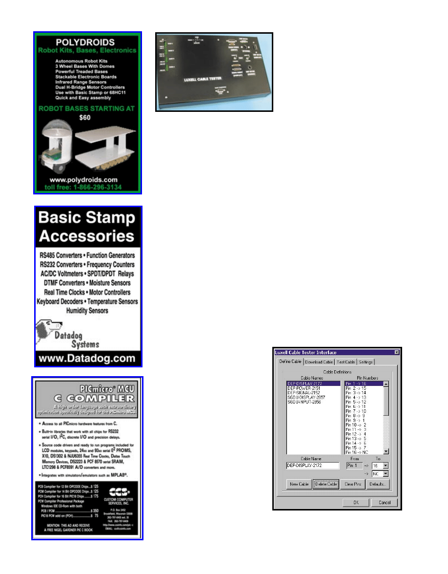
Photo 2—
A cable is selected from the leftmost list. The pin
definitions for that cable are shown in the rightmost list.
Clicking on a pin allows the pin connection to be altered
using the pop-up menus below the second list.
Photo 1—
A total of five cables can be tested when
the tester is operating as a slave to a host computer.
The pin LEDs are visible to the left of the photo, and
the status LEDs are located at the top left.

June 2–5, 2003
Donald E. Stephens
Convention Center
Rosemont, IL (Chicago)
Bigger!
Bigger!
America’s Largest Sensors Event
Just Got
More coverage of:
•
Biosensors
•
Wireless Networking
•
Smart Solutions and
Intelligent Systems
•
MEMS/MST
•
Nanotechnology
•
Plus an expanded 2-Day
Business of Sensors Symposium
Don’t delay. Register by April 21 for advance registration rates and receive
FREE exhibit hall and Industry Networking Reception admission (a $65 value).
www.cir.sensorsexpo.com or 800-331-5706.
Be sure to reference priority code 71 when registering.
Dean Kamen,
featured
speaker
at the “Spir
it of
Innovation”
luncheon
One badge gives you access
to three great shows:
—Sensors Expo & Conference
—International Robots & Vision Show and Conference
—Industrial Fastener & Forming International Exhibition and Conference
www.circuitcellar.com
CIRCUIT CELLAR
®
Issue 154 May 2003
19
STAND-ALONE AND DELIVER
When operating in Stand-Alone
mode, the cable tester uses the contents
of EEPROM to define one of four test
vectors to use during testing. You may
download additional EEPROM informa-
tion from the Circuit Cellar ftp site.
The EEPROM address represents an
implied pin number. Memory address
0x00 represents pin 1 for cable 1 and
address 0x7F represents pin 32 for
cable 4. The contents of each memory
location identify the pin that is con-
nected to the implied pin number. For
example, assume EEPROM location
0x10 holds a value 0x08. This means
that for cable 1, connector A, pin 17 is
connected to connector B, pin 8. (Note
that connector A is driven as connec-
tor B is read as an input.)
There are some limitations to the
Stand-Alone mode implied by the
fixed EEPROM size. Only a cable with
one-to-one or many-to-one pin map-
ping is supported. This means one or
more pins on connector A can be tied
to only one unique connection on
connector B.
If you were willing to
sacrifice the ability of
testing four cables and
instead limit the cable
tester to one cable at a
time, you could support
any pin mapping, because
you could hold an entire
32-bit result vector in
EEPROM for each pin of a
32-pin cable. In that case,
you would need 128 bytes
of EEPROM to store the
result vectors to allow
the testing of any cable.
In my case, most of the
cables I had to test were
either many-to-one or
one-to-one pin mappings,
so this wasn’t an issue.
There are no limitations
when using the PC-based
cable tester interface.
When testing a cable,
the
TestCable routine
begins by driving pin 1
low via the
pdrvStart()
function (see Listing 2).
Next, all 32 input pins
are scanned and assem-
bled—using
prcvScanAll()—into a
32-bit result vector that’s kept in vari-
ables
b0, b1, b2, and b3. Note that b0
holds the most significant byte corre-
sponding to input pins 25 through 32.
The most significant bit of this byte
represents input pin 32. Then, the
result vector is then bit-wise inverted,
and the algorithm uses the current pin
that’s driven to index the EEPROM
cable vectors and retrieves the pin
number (
tpin) that should be driven.
Assuming that
tpin is
nonzero (i.e., is not open-
circuit), you can check
whether or not the bit cor-
responding to
tpin is set
in
b0 to b3 using the
vecIsSet() function. If
this bit is set, the corre-
sponding bit in the
b0-to-b3
result vector is cleared and
the algorithm continues.
If the bit isn’t set, which
means you’ve detected an
open circuit, an open-cir-
cuit error is set using the
errSet() function.
Next, a test is performed
to see whether any other bit
is set that would indicate a
short circuit from the driv-
ing pin to the shorted pin.
If another bit is found set
in the result vector, the
errSet() function is called
with a short-circuit error.
The
pdrvNext() function
drives the next pin in
sequence, and the afore-
mentioned steps are repeat-
ed to detect any errors
for this pin.
Reset
Initialize I/O
and RS-232
port
Turn on
Ready LED
rsGreeting
Display initial greeting
on any attached
RS-232 device
SCI input?
N
Y
Scan push
buttons
GetCommand
Active
button?
N
Y
Clear logged
test errors
TestCable
EEPROM
cable vectors
errReport
Sequentially drive all
outputs, verify results against
EEPROM cable vectors and log errors
Flash pin LED and the
Open/Close LEDs to
report any logged
errors
Process commands
from the host computer
to write cable vectors
to EEPROM or execute
a test vector and return
the results
Figure 4—
The top-level PIC software shows the initialization, stand-alone, and remote-
cable test paths. The
GetCommand
routine provides cable definition downloads and
remote test capabilities.
Figure 3—
The 7407 open-collector buffers isolate the cable to be tested so that only the driven LED illuminates.
These drivers also provide high-voltage protection against accidental ESD discharges into the cable tester pins.

20
Issue 154 May 2003
CIRCUIT CELLAR
®
www.circuitcellar.com
If you’re observant, you’ll discover
the
rsPut() and rsPutHex() func-
tions strewn about the code. These rou-
tines provide an external diagnostic
capability when the stand-alone cable
tester is connected to an external ter-
minal or terminal emulator on a PC.
For each tested pin, a report is generat-
ed containing the result vector, the
source and destination pins, and the
pass/fail test condition. A typical report
would be
V00000001 0701T<CR>. This
means the test was performed from
connector A, pin 7 to connector B, pin 1
with a result vector of 0x00000001 (or
pin 1 is active). It passed successfully.
HOW IT WORKS
Several examples will clarify how
the cable tester detects open and short
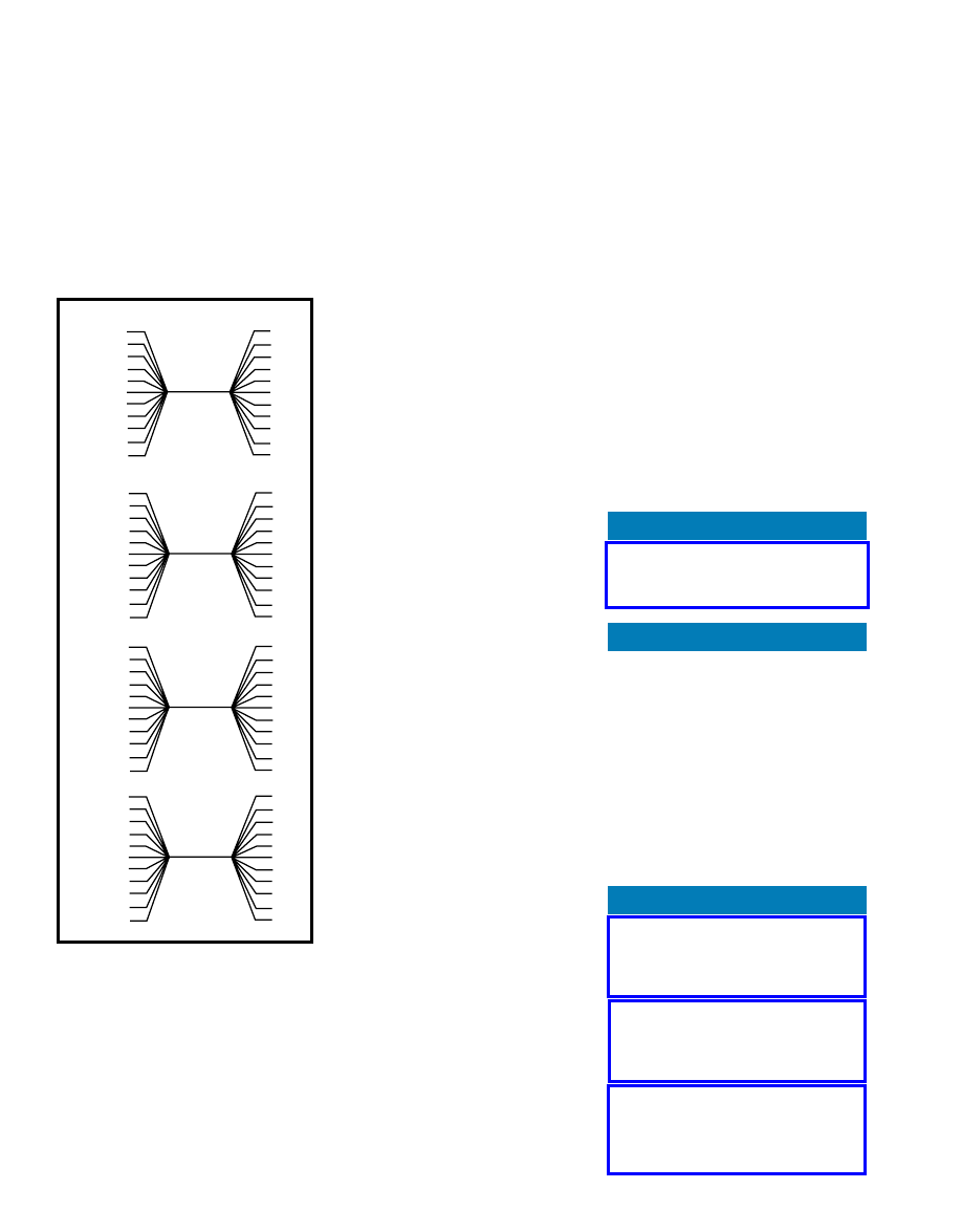
circuits. If pin 1 is driven as shown in
Figure 5a, there are four possible out-
comes: an open circuit where the
result vector becomes 11111111111;
one pin (6) is driven to give a result
vector of 11111011111 (see Figure 5b);
multiple pins (6 and 9) are driven to
give a result vector of 11011011111
(see Figure 5c); or multiple pins (1 and
4) are connected to the same pin to
give a result vector of 11111011111
(see Figure 5d).
Figure 5a illustrates an open-circuit
result. Depending on whether or not
the current pin test vector should be
open circuited, this could be either an
error or a valid result. Figure 5b shows
the most typical case of a one-to-one
mapping, where a pin on one side of the
cable is connected to a pin on another
side of the cable. If the required pin
isn’t found where it’s expected, an
open-circuit fault is generated.
Figure 5c shows a one-to-many pin
mapping. In Stand-Alone mode, the
cable tester cannot handle this particu-
lar scenario. There is a reason for this.
Because you can store only one pin con-
nection for each pin that’s driven, you
have no way of showing multiple pins
connected to the driving pin. Of course,
any one-to-many mapping can be easily
turned into a many-to-one mapping
simply by reversing the cable ends.
Figure 5d illustrates a many-to-one
pin mapping. This scenario is support-
ed in Stand-Alone mode because each
pin on the drive side has stored a sin-
gle connection in EEPROM. Thus,
pins 1 and 4 will be connected to pin 6.
Naturally, these examples are sim-
plified and, in the real world, will
often be combined. Thus, many-to-
many connections may be found
together with some pins shorted and
others remaining open.
Listing 1—
The
GetCommand()
function is responsible for processing commands received from the host
computer. Two modes are available: the first programs the PIC EEPROM with a received data byte; the sec-
ond initiates a pin test and responds with a test vector.
procedure GetCommand is
var byte adr,
--Write EEPROM address
data
--EEPROM data to write
inbuf = rsGet()
--Looking for Pxx yy<CR> command
if inbuf == "P" then
--Get the EEPROM address
adr = rsGetHex()
if ! CheckNum(adr, 0x7F) then return end if
--Get space character
if ! CheckChar(" ") then return end if
--Get the pin number
data = rsGetNum()
if ! CheckNum(data, 32) then return end if
inbuf = rsGet()
if inbuf != ASCII_CR then
--Error: expecting <CR>
rsPutNak()
return
end if
--Program EEPROM data
if vecProgram(adr, data) then
rsPutOK()
--Programmed location OK
else
rsPutNProg()
--Error: couldn't program EEPROM
end if
--Looking for Txx<CR> command
elsif inbuf == "T" then
data = rsGetNum()
if ! CheckNum(data, 32) then return end if
inbuf = rsGet()
if inbuf != ASCII_CR | data == 0 then
--Error: expecting <CR>
rsPutNak()
return
end if
--Output test vector to pins
pdrvPut(data - 1)
--Scan the inputs
var byte b0, b1, b2, b3
prcvScanAll(b0, b1, b2, b3)
if ! DEBUG then pdrvPut(POWER_LED) end if
--Output the scanned results
rsPut = "V"
rsPutHex(b0)
rsPutHex(b1)
rsPutHex(b2)
rsPutHex(b3)
rsPut = ASCII_CR
--Otherwise we have an error
else
GetCR()
rsPutNak()
end if
end procedure

www.circuitcellar.com
CIRCUIT CELLAR
®
Issue 154 May 2003
21
GETTING SOME RESPECT
These days, if you don’t have a fancy
GUI, nobody gives you any respect.
The PC-based cable-test program was
designed to provide a friendly interface
to define, modify, and download test
cables from a PC and get some respect
from people who’d rather deal with
software than hardware. Another
advantage of the PC-based interface is
that cable-test results can be saved to
disk. This provides a permanent
record of each cable’s test for quality
assurance or audit purposes.
Take a look at Photo 2. After the
program starts, it displays several
panes: four tabbed panes comprising a
definition pane to define the cables; a
download pane to program the PIC
EEPROM with up to four cable defini-
tions; a test pane to remotely test a
selected cable; and a settings pane
that changes some default behaviors
(e.g., where the cable definitions are
stored and which COM port to use
(not working)).
The default cable definition directo-
ry is located in the installation direc-
tory under the name “Cables.” I
wouldn’t advise changing any of the
default settings unless, like me, you
know what you’re doing.
The PC-based software program is
connected via a serial link (9600 bps,
8 bits, no parity, 1 stop bit) to the
cable tester. You may download the
executable for this program from the
Circuit Cellar
ftp site. Installation is
straightforward. The program should
operate on any PC running Windows
95/98 or NT. It has not been tested
under Windows 2000 or XP, but it
should work.
There are some limitations, as well.
Only COM port 1 is currently sup-
ported, because I didn’t have good
serial interface driver routines for
C++. So, I used the default serial class,
which was terrible. Another limita-
tion is that if you’re entering text in
an input string and hit Enter, the pro-
gram will exit.
CABLE BY ANY OTHER NAME
To define a new cable, click on the
Define Cable tab. If preinstalled cables
exist in your Cables directory, they
will appear in the list box as shown in
Photo 2. The pin definitions appear in
another scrolling list to the right of
the cable names. The highlighted
cable’s pins are always shown. If a par-
ticular pin connection is highlighted,
it can be edited by selecting different
To connections in the area below the
pin definitions. Up to two connec-
tions per pin can be selected.
As you know, the cable tester only
understands single-pin connections. It
will happily lock up and die if you try
to download a cable with a double-pin
connection. So, why include this fea-
ture? Well, when using the PC to
remotely test cables, double-pin con-
nections are allowed because the PC
performs the cable test.
Listing 2—
The
TestCable()
function performs the stand-alone cable testing functions. EEPROM test
vectors are compared with the cable to prepare a fault log and, at the test’s conclusion, flash the pin and
status LEDs to give a fault indication.
procedure TestCable (byte in vector) is
var byte tpin,
--Current test vector pin ID
dpin
--Current driving pin ID
--Drive each pin sequentially
pdrvStart()
while ! pdrvDone() loop
--Scan all the inputs
var byte b0, b1, b2, b3
prcvScanAll(b0, b1, b2, b3)
if ! DEBUG then pdrvPut(POWER_LED) end if
--Negate the test vectors
b0 = ! b0
b1 = ! b1
b2 = ! b2
b3 = ! b3
--Look up desired pin connection
dpin = pdrvPin()
tpin = vecLookup(vector, dpin)
rsPut = "V"
rsPutHex(b0)
rsPutHex(b1)
rsPutHex(b2)
rsPutHex(b3)
rsPut = " "
rsPutHex(dpin)
rsPutHex(tpin)
--Test whether the connection is good
if tpin != 0 then
if vecIsSet(tpin, b0, b1, b2, b3) then
vecClrBit(tpin, b0, b1, b2, b3)
rsPut = "T"
else
--Generate an open-circuit error
errSet(OPEN, dpin, tpin)
rsPut = "F"
end if
end if
rsPut = ASCII_CR
var byte vbit = 1
while vbit <= 32 loop
if vecIsSet(vbit, b0, b1, b2, b3) then
errSet(SHORT, dpin, vbit)
end if
vbit = vbit + 1
end loop
pdrvNext()
--Drive the next pin
end loop
end procedure
22
Issue 154 May 2003
CIRCUIT CELLAR
®
www.circuitcellar.com
Michael Griebling graduated from the
University of Waterloo with a BSEE.
He has been designing embedded
hardware, software, and firmware in
the aerospace industry for the past
20 years. Currently, he’s the senior
electrical engineer for the High
Performance Display group at Luxell
Technologies located in Mississauga,
Ontario. His interests include pro-
gramming in obscure computer lan-
guages (e.g., Ada, Oberon-2, JAL, and
Modula-2), learning about neural net-
works and fuzzy logic systems, and
helping with the HCS II. You may
reach him at mgriebling@luxell.com.
To create a new cable, click on the
New Cable button. An empty cable
with all NC connections should
appear highlighted. Change the name
by editing the Cable Name field.
Click on pins to change the pin con-
nections using the pop-up menus
located below the pin list.
When you’re done, you can exit the
program, because cable definitions are
always stored on disk. Be cautious
with older operating systems. They
still may have an eight-character
name limit for files, because the cable
definitions are stored as files in the
Cables directory with the cable name
as the file name. Select a cable to
either delete the entire cable by click-
ing on the Delete Cable button or
clear the pin numbers by clicking on
the Clear Pins button.
GET DOWNLOADING
Click on the Download Cable tab to
view the download pane. The same
cables that were defined will be avail-
able from each of the pop-up menus
for cables 1 through 4.
After the cables to be downloaded
are selected, click on the Download
Cables button to initiate the down-
load to the cable tester. (Don’t forget
to connect the PC to the cable tester.)
A progress indicator will show the
download status. If any cables are left
blank, they will not be downloaded.
REMOTE TESTING
Click on the Test Cable tab to view
the cable-test pane. The same cables
that were defined will be available for
the Cable ID pop-up menu. There are
also two fields used to fill in an opera-
tor’s name and a work order identifier
for cable-test reports that will be kept on
file. A date will be automatically added.
Click on the Test Cable button (it
helps the test to pass if a cable is con-
nected), and a series of pass/fail mes-
sages will appear in the report win-
dow. Wait until the test is completed
(all 32 pins are always tested, even if
only two pins are used), and then click
on the Save Report button to save the
test results to disk. You may down-
load a sample test report from the
Circuit Cellar
ftp site.
THAT’S ALL FOLKS
Although the cable tester program
tour was a bit of a whirlwind, it’s fair-
ly easy to use thanks to the GUI. You
shouldn’t have any problems, but if
any arise, you may reach me via e-
mail. Because of my current workload,
I can’t promise an immediate
response, but I will eventually reply.
The cable tester has been actively
used in my company’s production area
Cable under test
0
1
1
1
1
1
1
1
1
1
1
1
2
3
4
5
6
7
8
9
10
11
1
1
1
1
1
1
1
1
1
1
1
1
2
3
4
5
6
7
8
9
10
11
Pin Drive
Vector Pin
Cable under test
0
1
1
1
1
1
1
1
1
1
1
1
2
3
4
5
6
7
8
9
10
11
1
1
1
1
1
0
1
1
1
1
1
1
2
3
4
5
6
7
8
9
10
11
Pin Drive
Vector Pin
Cable under test
0
1
1
1
1
1
1
1
1
1
1
1
2
3
4
5
6
7
8
9
10
11
1
1
1
1
1
0
1
1
0
1
1
1
2
3
4
5
6
7
8
9
10
11
Pin Drive
Vector Pin
Cable under test
0
1
1
0
1
1
1
1
1
1
1
1
2
3
4
5
6
7
8
9
10
11
1
1
1
1
1
0
1
1
1
1
1
1
2
3
4
5
6
7
8
9
10
11
Pin Drive
Vector Pin
Figure 5a—
If the EEPROM pin number is zero or
open circuit, this result is valid; however, in all other
cases, this would be an open-circuit fault condition.
b—
If the target pin location does not match the inter-
nal EEPROM pin number, an open-circuit fault is gen-
erated.
c—
This pattern cannot be supported in Stand-
Alone mode. When operating with an external host,
checks are performed to determine whether or not
all of the target pins do in fact map to the driving pin.
If a pin is not found, it is flagged as a short circuit.
d—
The tester handles this situation like the one-to-
one mapping where any missing connection is
detected as an open-circuit fault. Any unexpected
connections are logged as short-circuit faults.
a)
b)
c)
d)
PROJECT FILES
REFERENCES
[1] W. van Ooijen, JAL Manual,
1999.
[2] Microchip Technology, Inc.,
PIC16F62X Flash-based 8-bit
CMOS Microcontroller
,
DS40300C, 2003.
[3] National Semiconductor Corp.,
LM2670 Simple Switcher High
Efficiency 3A Step-Down
Voltage Regulator with Sync
,
DS100942, 2000.
SOURCES
PIC16F628 Microcontroller
Microchip Technology, Inc.
(408) 792-7200
www.microchip.com
LM2670 Switching regulator
National Semiconductor Corp.
(800) 272-9959
www.national.com
74HCT138 Decoder
Philips Semiconductors
(800) 326-6586
www.semiconductors.philips.com
for almost a year. So far, no problems
have been reported.
Finally, I would like to thank every-
one at Luxell for helping to make this
project possible. Happy testing!
I
Flash
Facts
$49
.95
($199 Value)
Now for a limited time
ZiLOG redefines 8-bit with the new Z8 Encore!
™
family
of flash microcontrollers that simplifies your development
process, increases design productivity and gives you
more functionality than any other 8-bit MCU in history.
But don’t take our word for it.
Visit us at www.zilog.com/Z8encore2 or
call us at 866-498-3626 and receive our complete
development kit for only $49.95.
Act now because when this special introductory
offer ends, the kit will sell for $199.95!
Z8 Encore!
™
will be available in all standard flash memory
configurations from 4K to 64K. Incorporated into new
designs or upgrading from existing 8-bit (including Z8
®
)
architectures, this next-generation MCU has features
and performance that leaves the competition in the dust.
The Z8 Encore!
™
Test Drive Kit Includes
Hardware
• Evaluation Board
• Target Interface Module Board
• Serial Cable
• Universal Power Supply
Software
• ZDS II IDE with full
version C-compiler
• Sample Code
• Device Drivers
• Documentation CD
The New Z8 Encore!
™
MCU Block Diagram
10-bit A/D
Converter
Port A Port B Port C Port D Port E Port F Port G Port H
16-bit Timer
w/PWM
16-bit Timer
w/PWM
16-bit Timer
w/PWM
16-bit Timer
w/PWM
I
2
C
SPI
UART 0
UART 1
Watch-Dog
Timer
Crystal
Oscillator
Register File
4K X 8
DMA
Controller
Interrupt
Controller
eZ8
20MHz
CPU
Reset
Control
On-Chip
Debugger
Flash
Program
Memory
64K X 8
THE
THE
Z8
ENCORE!
™
ZiLOG, Z8 Encore! and Z8 are trademarks or registered trademarks of Zilog Inc. in the United States and in other countries. Other logos, product names and service names mentioned herein may be trademarks of the companies with which they are associated.
This comparison is valid as of 9/27/2002.
FEATURE
ZILOG
MOTOROLA
ZILOG
MOTOROLA
Z8F6403
MC68HC908AS60A
Z8F3202
MC68HC908GP32
Actual CPU Speed
20MHz
8MHz
20MHz
8MHz
On board DMA
Yes
No
Yes
No
High Speed Flash
64K
60K
32K
32K
SRAM
4K Bytes
2K
Bytes
2K Bytes
512
Bytes
A/D Converter
10-bit
8-bit
10-bit
8-bit
SPI & I
2
C
Both
No
I
2
C
Both
No
I
2
C
UARTs
2 (9-bit)
1
(8-bit)
2 (9-bit)
1
(8-bit)
16-bit Timers
4
Multi-mode 2
Multi-channel
4
Multi-mode 2
Multi-channel
Independent
Synchronous
Independent
Synchronous
Timers
Timers
Timers
Timers
24
Issue 154 May 2003
CIRCUIT CELLAR
®
www.circuitcellar.com
t was time to
buy a new car. Oh,
I probably could have
squeezed another
10,000 miles out of my old ride, but
quite honestly, I had become bored
with it. I was tired of sitting every day
in the same old interior, hearing the
same old creaks and rattles. I wanted
something new, something exciting,
and something, well, different.
So, being your typical obsessive
engineer, I pored over mountains of
brochures, bought stacks of car maga-
zines, and clicked through hundreds
(perhaps thousands) of on-line road
tests in search of the perfect vehicle. I
analyzed stopping distances and safety
ratings, and evaluated cornering val-
ues and slalom times. These figures
and more were charted, noted, and
mulled over again and again. But
unbeknownst to me, my decision had
been made for me several weeks
before—by my teenage daughter.
“Dad, you have to get a New Beetle.
They’re so cute!” she pressed, signifi-
cantly pruning my decision tree to one
of mere price, color, and interior.
“No dad, you have got buy the
blue one.”
OK, price and interior. Well, at
least it was different.
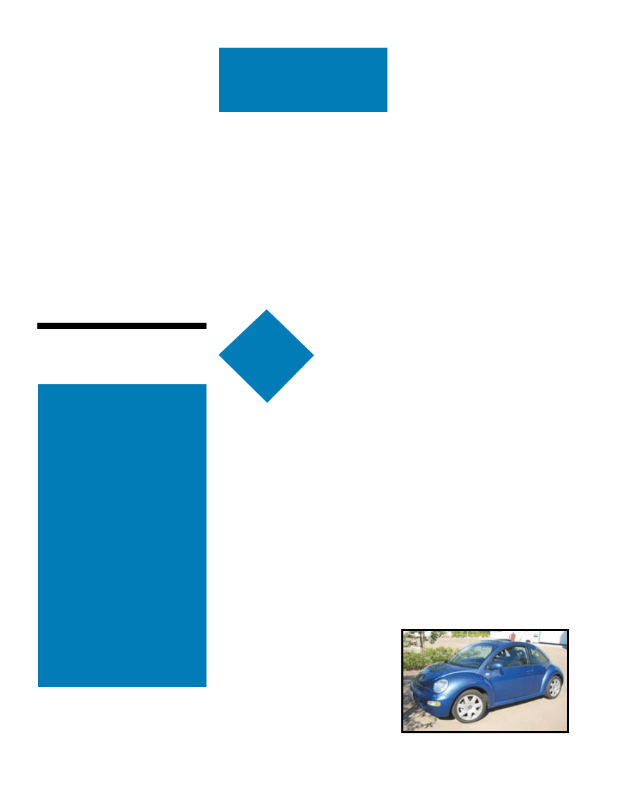
Not long after my purchase (I
ordered the blue lagoon paint option
with black leather seats), I began won-
dering how the car’s performance fig-
ures would compare to the numbers
published in the automotive press (see
Photo 1). Would they hold up, or were
those specs just exaggerations like the
profit/loss statement of a certain bank-
rupt Texas-based energy company?
Comparing 0-to-60 times and brak-
ing forces would have been simple: a
stopwatch and tape measure could
have easily supplied those values. But
the measurement of lateral accelera-
tion remained puzzling. And, for a com-
pact, my car’s values were high, 0.81 g,
which is BMW 745 territory. Simple
mechanical instruments that measure
G-forces were impractical in an auto-
motive environment, and modern elec-
tronic meters were too expensive for an
enthusiast’s pocketbook—especially
one with new monthly car payments.
DESIGN GOALS
Undeterred, I began devising a way
to make my own G-force meter. I
came up with a few design goals. First
and foremost, the meter had to be rel-
atively simple and inexpensive to
build. Second, I wanted to make it
easy to install in any car. Drilling
mounting holes in my New Beetle
was not an option. Finally, it had to be
able to read out accurately to one hun-
dredth of a G—just like the car maga-
zines. With those goals in mind, I then
had to find a sensor.
SENSORY OVERLOAD
Searching the Analog Devices web
site turned up a few candidates. One
sensor in particular seemed like a good
fit for my application. The ADXL202E
Automotive G-Force
Meter
i
How accurate are the
specs car companies
publish in their glossy
brochures? Asking
himself the same
question, Ross decid-
ed to challenge a
factory’s numbers
with his own G-force
meter. Not only is the
meter inexpensive, it
fits on the lid of an
ordinary travel mug.
Ross Tsukashima
FEATURE
ARTICLE
Challenging the Factory Specs
Photo 1—
This is my blue lagoon New Beetle with an
optional G-force meter on its roof. Your mileage may
vary. Title, taxes, and batteries are not included.
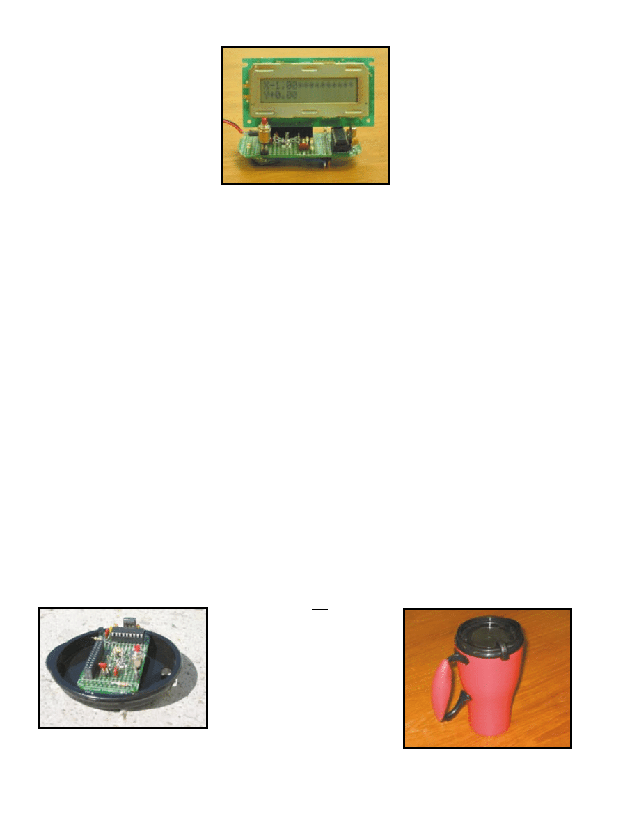
www.circuitcellar.com
CIRCUIT CELLAR
®
Issue 154 May 2003
25
the need for additional performance.
If you need to sample more fre-
quently, the internal sensor’s demod-
ulator outputs can be read directly
from the X and Y filter pins. This
analog voltage signal is ratiometric,
and it runs about 300 mV/g when
supplied with 5 V.
KEEP IT BASIC
My software-related goals were to
give you both a numerical and graphi-
cal representation of the data on the
LCD, and include a calibration routine
that utilized the PIC’s nonvolatile
memory for saving correction factors.
Because it was my first experience
with the ADXL202E, I had some trepi-
dation about interfacing the sensor to
the micro. Fortunately, while review-
ing some of the technical support
information on Analog’s web site, I
found examples showing how to easily
convert the pulse-width lengths into
acceleration values using PicBasic’s
Pulsin command. [2]
After the program starts executing,
the first thing that occurs is the load-
ing of the calibration correction val-
ues from nonvolatile memory using
the read command. Because the vari-
ables are declared as 16 bits, two
reads are required to construct the
data from memory.
Next, the microprocessor is instruct-
ed to read the x- and y-axes PWM
lengths. The data is read multiple
times, averaged, and then checked
against a zero constant to evaluate
whether to flag the data as a plus or
minus g value. With a 4-MHz oscilla-
tor, the
Pulsin command returns the
number of counts that the line was
is a tiny 8-pin LCC surface-mount com-
ponent that contains two accelerome-
ters arranged perpendicular to each
other. In addition, it converts its output
to a digital pulse width, so any embed-
ded micro with a timer/counter can
easily decode the values.
The ’202E’s sensing range is
±
2 g
with a 1000-g maximum unpowered
shock rating, which is perfect for but-
terfingers like me who tend to drop
things during assembly. Because auto-
motive lateral acceleration forces
rarely exceed 1 g, selecting a sensor
with a lower range allows for a larger
signal output for a given force.
SIX EASY PIECES
Only six major components are
required to build the G-force meter.
Obviously, the sensor is one of them.
The remaining pieces include the
micro, an LCD, a good 5-V regulator, a
momentary switch, and an oscillator.
(The count is five if you use a micro
that has its own internal oscillator.)
With the sensor squared away, I
started evaluating the number of I/O
pins required for the microprocessor.
A quick review of the ADXL202E’s
datasheet revealed that the accelerome-
ter would need three pins—two for the
PWM outputs and one for a self-test
line. Adding an LCD (7) and momen-
tary switch for selecting calibration (1)
would bring the total up to 11. It start-
ed to sound like a job for a PIC.
Microchip’s ubiquitous PIC16F84A
sports 13 I/O lines and 2 KB of flash
memory, and MicroEngineering
Labs’s PicBasic Pro supports it. From
a hardware and software perspective,
it seemed to be a good fit.
PicBasic supports LCD modules
with an Hitachi 44780 controller or
its equivalent. I used an old Hitachi
LM016L 2 × 16 unit for my display,
but a unit like Optrex’s DMC-16207
would work just as well (see Figure 1).
SENSOR DETAILS
The duty cycle modulator (DCM) is
configured to generate a 50% duty
cycle at 0 g. Higher values produce a
longer pulse, and lower values gener-
ate a shorter one. The complete duty
cycle duration (high and low) is user
adjustable; it ranges from 0.5 to 10 ms
depending on the value of the resistor
connected to pin 2. The sensor’s inter-
nal pulse-width converter has 14 bits
of resolution, although real-world
accuracy would probably be somewhat
less because of the accelerometer’s
minimum noise floor.
The bandwidth for each axis can
be tuned by selecting appropriate
capacitors using the following for-
mula obtained from the ADXL202E’s
datasheet:
A minimum capacitance value of
1000 pF for Cx and Cy must be used
to ensure proper operation. To reduce
errors, the datasheet includes the rec-
ommendation that the bandwidth be
one-tenth of the DCM frequency. I
was conservative with my initial val-
ues, and set the pulse width to 10 ms
with a bandwidth adjusted to a leisure-
ly 5 Hz. Later, during testing, it would
be easy enough to change if I felt
F
F
C
−
3
5
dB
=
µ
Photo 2—
The LCD shows the acceleration direction
(
±
), calculated value, and a graphical representation of
force for each sensor. Each asterisk represents one
tenth of a g.
Photo 3—
The accelerometer sensor chip is mounted
dead-bug style with double-sided tape. I custom fitted
the PC board using a bench grinder to allow for instal-
lation in the cup’s lid.
Photo 4—
My travel mug has a removable lid. Note the
tapered base and lipstick-red housing.
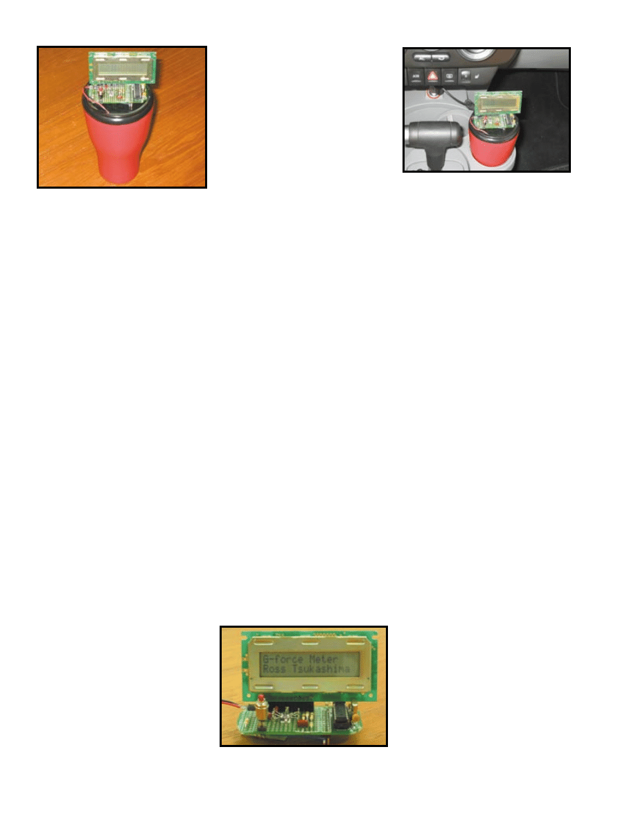
26
Issue 154 May 2003
CIRCUIT CELLAR
®
www.circuitcellar.com
high in 10-µs increments. Because the
duty cycle output is set to 10 ms, the
zero point (or the 50% duty cycle) of
each axis is typically in the range of
approximately 500 counts, or 5 ms.
The calibration subroutine utilizes
the force of gravity to preload the sen-
sor. Slowly tilt the sensor in one direc-
tion until you find the maximum
value, and then flip the sensor over
and look for the minimum. Pressing
the calibration button during each
step automatically saves these num-
bers in nonvolatile memory locations
with the write command.
Subtracting the minimum from the
maximum count and dividing by two
provides you with the magic 1-g con-
stant. Adding this number to the min-
imum count value gives you the actu-
al midpoint value for 0 g.
These constants are all that are
required to turn the counts into accel-
eration. The G-force values are then
calculated (be careful not to lose sig-
nificant digits during division) and
painted on the LCD screen along with
a plus or minus sign to signify direc-
tion and the appropriate amount of
asterisks, which are placed after the
numeric value to graphically represent
magnitude (see Photo 2). When it was
all said and done, I had somehow
managed to occupy all but 4 bytes of
code space in the PIC. Talk about
cutting it close.
DEBUGGING
Being the victim of more than my
share of catastrophic failures (other-
wise know as “zorching”) during ini-
tial start-ups, I’ve made a habit of
hooking up a DMM to monitor cur-
rent when flipping the switch. For-
tunately, there were no fabrication
slip-ups this time, and the DMM dis-
played about 6 mA of total operating
current (see Photo 3).
During the initial trials, I noticed
quite a bit of jitter in the output
when the unit was plugged into my
car. I attributed most of the extra
noise to engine vibrations, but I later
noticed that the noise appeared to be
the same whether the car was run-
ning or shut off.
Analog Devices recommends a
100-
Ω
(or smaller) resistor or ferrite
bead be used in conjunction with a
0.1-µF decoupling capacitor on the
power supply line. The idea is to
reduce interference when the sensor
shares power with the microproces-
sor. I decided to experiment and add
the recommended resistor and capac-
itor combination to see if it could
improve this situation. It was amaz-
ing how much of an effect this small
change made. Signal variations of
more than 30 counts instantly disap-
peared from my display.
With the signal jitter whipped, I
decided to experiment a little more by
trying to increase the bandwidth val-
ues. Through empirical means, I deter-
mined that I could decrease the capac-
itor values to 0.1 µF without experi-
encing any obvious detrimental
effects. This gave me a calculated
bandwidth of 50 Hz, which seemed
more appropriate for the task at hand.
DOUBLE-ESPRESSO SOLUTION
One of the more difficult aspects of
this project involved coming up with
a standard way to mount the meter in
a car without having to resort to
drilling, gluing, or duct taping. As I
was mulling this problem over a dou-
ble espresso at Starbucks one morn-
ing, I noticed that the bottoms of the
commuter coffee cups people were
carrying were all the same size. I
quickly came to the realization that
they were standardized to fit in
almost any car’s cup holder.
Aha! That was it. Design a housing
to fit a standard cup holder. Better
yet, find a commuter cup that could
be used as the housing. The cup
holder mount could keep the sensor
flat, which would provide a more
accurate output signal during use.
And, because of its location near a
power outlet, the power cord’s length
could be kept to a minimum. Best of
all, the cup holder was already built
in. No installation required.
Browsing the local Target depart-
ment store, I located a nearly ideal
travel mug. The mug’s base was
small enough to fit in the cup holder
frame, and its top was large enough
to hold both the circuit board and
LCD (see Photo 4).
After completing the housing, I
installed the G-force meter and took
a quick jaunt around the block. The
cup tended to tip slightly in the cup
holder frame during some of the
more extreme maneuvers. Cutting 1
″
off the bottom of the cup seemed to
give it a tighter fit and eliminated
the tipping (see Photo 5).
TEST RESULTS
Before describing my testing experi-
ences, I want warn you about the dan-
gers of testing a moving automobile at
the limits of adhesion while periodi-
cally diverting your attention to
squint at a small, vibrating LCD.
Photo 6—
Mounted in the test vehicle’s cup holder, the
meter was conveniently in close proximity to the 12-V
power outlet.
Photo 7—
It’s always a good feeling to see your name
displayed on the LCD when powering up for the first time.
Photo 5—
I was ready for the test ride as soon as the
finished hardware was mounted on coffee cup’s lid.
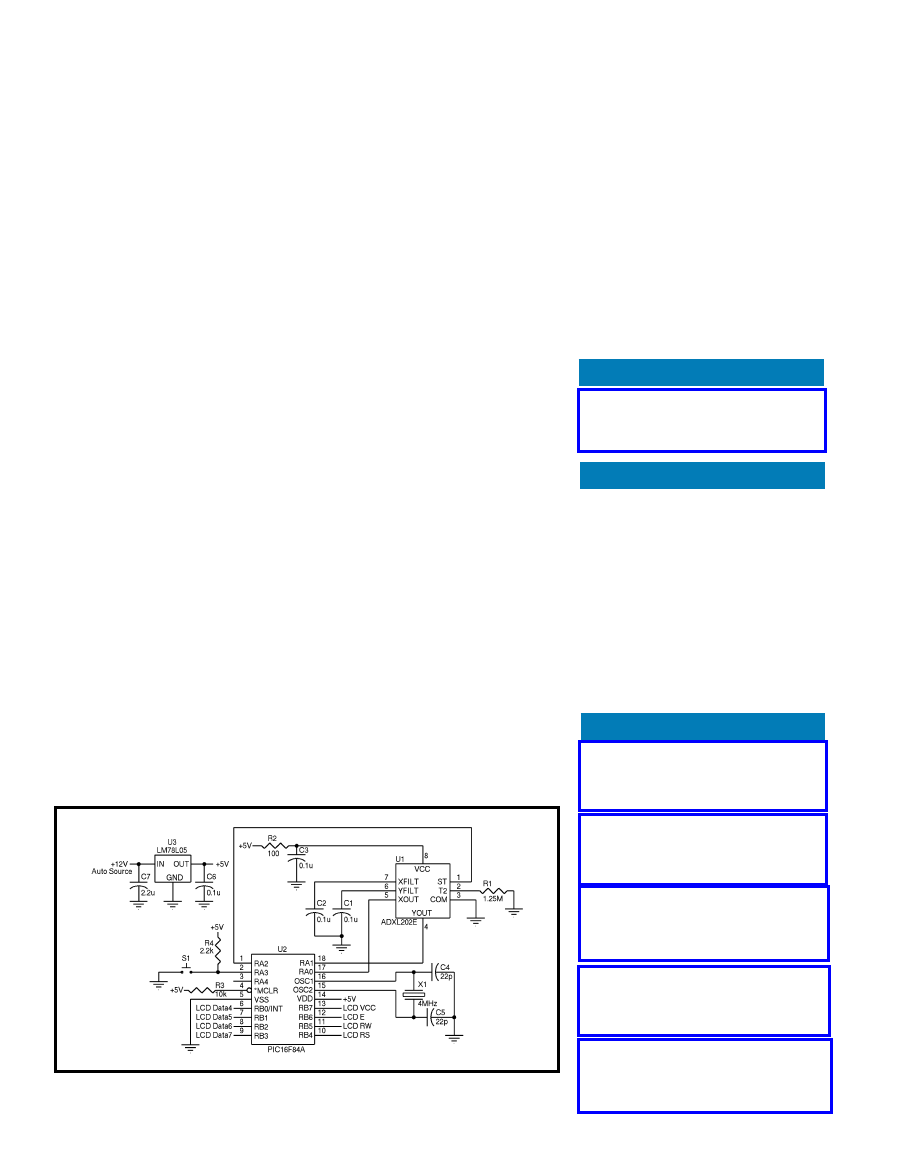
REFERENCES
[1] Analog Devices, Inc., “Low-
Cost
±
2 g Dual Axis
Accelerometer with Duty
Cycle Output,” rev. A, C02064-
2.5, October 2000.
[2] H. Weinberg, “Using the
ADXL202/ADXL210 with the
Parallax Basic Stamp Module to
Speed Algorithm Development,”
rev. 0, Analog Devices, Inc.,
September 1999.
www.circuitcellar.com
CIRCUIT CELLAR
®
Issue 154 May 2003
27
Testing acceleration forces involves
some risks, so the process should be
conducted by professionals under
controlled conditions.
I had more fun than a barrel of
monkeys testing this device. The
meter seemed to work exactly as I
had planned: it scrolled out values
when I accelerated, read the G-forces
when I turned left and right, and
changed signs to minus during brak-
ing. It’s a wonder I didn’t get a traffic
ticket (see Photo 6).
Using a wide, sweeping (and
empty) highway off-ramp near my
house, I found that my New Beetle
could easily meet (and sometimes
momentarily exceed) the 0.81-g force
value published for my car. Mission
accomplished. All of the automotive
magazines told the truth. Not that I
ever doubted them.
ROOM FOR IMPROVEMENT
Upgrading to a larger microproces-
sor could open the floodgates for new
design options. Now, I’ll describe a
few of them.
When you are measuring G-forces
using two-axis components, sensor
values can be distorted if the device
is not positioned exactly perpendi-
cular to the moment of force. In
other words, any tilting of the sen-
sor will reduce its measured output
values. Note that adding a third z-
axis component could theoretically
assist in compensation by allowing
for the ability to compute a total
vector sum.
A car’s interior can experience a
wide range of temperature varia-
tions. If you were to go through the
trouble of adding a third axis, it
wouldn’t hurt to go the extra mile
and add some sort of temperature-
compensation scheme.
One feature I’d really like to see is
an RS-232 port. This would allow
real-time data logging without having
to avert any attention from driving.
Such an addition wouldn’t be too dif-
ficult to implement. For instance,
you could use PicBasic’s
SEROUT
command to drive a serial interface
device like Maxim’s MAX232 chip.
In addition, I think a backlit graphi-
cal display would be neat. And so
would peak indicators.
Overall, I’m satisfied with how this
project turned out (see Photo 7). With
only six major components, it was a
cinch to build. The commuter cup
housing worked well and held the
device securely during testing. Most
importantly, it allowed me to accu-
rately compare my car’s performance
to previously published test values.
An added bonus was finally learning
that my New Beetle was indeed per-
forming in accordance with published
performance specifications.
Hmm, I wonder what kind of cor-
nering forces Honda’s Odyssey mini-
van can generate?
“Honey, can I borrow your car for
a few minutes?”
I
Ross Tsukashima received his B.S. in
Engineering from California State
PROJECT FILES
To download the code, go to
ftp.circuitcellar.com/pub/Circuit_
Cellar/2003/154/.
SOURCES
ADXL202E Accelerometer
Analog Devices, Inc.
(781) 329-4700
www.analog.com
LM016L LCD
Hitachi, Ltd.
(800) 448-2244
www.hitachi.com
PIC16F84A Microcontroller
Microchip Technology, Inc.
(480) 792-7200
www.microchip.com
PicBasic Pro
MicroEngineering Labs, Inc.
(719) 520-5323
www.microengineeringlabs.com
DMC-16207 LCD
Optrex America, Inc.
(734) 416-8500
www.optrex.com
Figure 1—
The switch connected to pin RA3 on the micro activates the calibration subroutine. The resistor con-
nected to pin 2 on the sensor adjusts PWM.
University, Long Beach and has been
working in the medical device field
for over 18 years. Currently, he lives in
San Diego and works on new product
designs at Sierra Medical Technology
(www.sierramedical.com). His most
recent work involves developing ther-
apeutic products targeted to improve
cardiovascular dynamics, and he was
recently granted a patent for an
implantable gastroesophageal pH-
monitoring radio-telemetric probe. In
his spare time, Ross enjoys tinkering
with his electric guitar. You may
reach him at rtsandiego@yahoo.com.
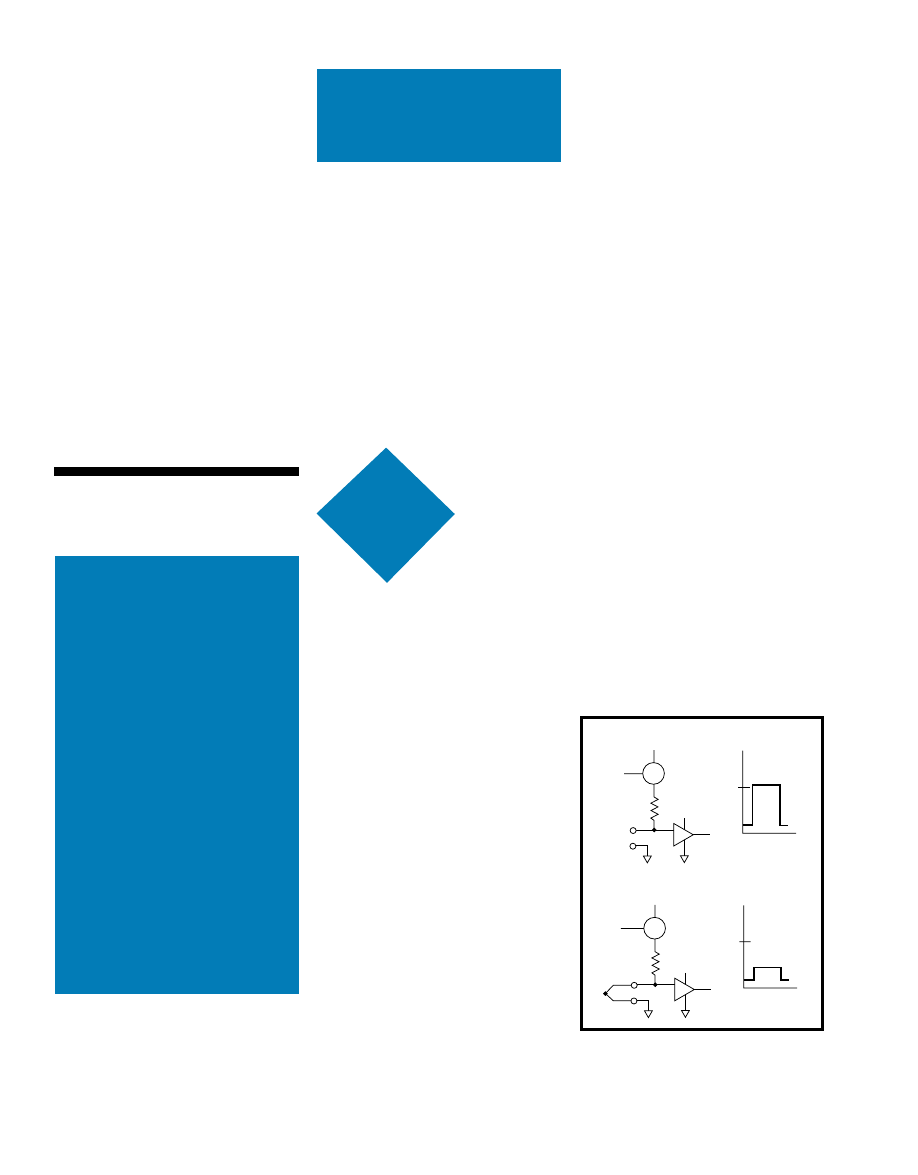
28
Issue 154 May 2003
CIRCUIT CELLAR
®
www.circuitcellar.com
traditional bar-
becue typically
involves cooking
tough cuts of meat (e.g.,
pork ribs, pork shoulder, and beef
brisket) over a wood or charcoal fire at
a low temperature (200° to 250°F). The
meat is cooked for long periods of
time until it’s tender (e.g., 5 to 6 h for
ribs and 10 to 20 h for brisket or pork
shoulder). Usually, steel offset cook-
ers, modified 55-gallon drums, and
even in-ground pits are used.
Another barbecue tradition requires
someone to be present for the 5 to
20 h that the meat is cooking. This
person must add fuel so the fire does-
n’t go out and regulate the cooking
temperature. Although modern tech-
nology can’t shorten barbecue-cooking
times, it can eliminate the need for
someone to be present to maintain the
cooking temperature.
CERAMIC COOKERS
Photo 1 shows a different kind of
cooker. The cooker’s thick ceramic
walls do such a good job of insulating
that a single load of lump charcoal
fuel can maintain barbecue-cooking
temperatures for more than 24 h. This
neatly solves the problem of having to
add fuel during a cooking session, but
there’s still the issue of temperature
regulation. The firebox is at the bot-
tom of the cooker, and the tempera-
ture is adjusted using the lower and
upper draft openings. Additional air
moving through the cooker produces a
bigger fire and higher temperature.
After it’s set for a given temperature,
a ceramic cooker does a remarkable
job of maintaining that temperature.
However, if internal or external condi-
tions shift too much (e.g., changes in
the weather or wind, or ash buildup in
the firebox), the draft settings must be
adjusted in order to keep the tempera-
ture from changing. To have true
hands-off temperature control, you
need a closed-loop process control sys-
tem. In such a system, the actual
cooker temperature is monitored and
used to adjust the airflow to maintain
the desired temperature.
PROJECT GOALS
The original goal for this project was
to implement a simple closed-loop tem-
perature controller using an 8-bit micro-
processor. Modeled after a kitchen oven,
I wanted the controller to have a knob
for setting the desired temperature. A
temperature probe would monitor the
ceramic cooker’s actual temperature,
and the controller would adjust the
airflow to keep the desired and actual
temperatures as close as possible.
a
Most chefs would
argue that barbecuing
is more art than sci-
ence. Nevertheless,
John introduced
ATmega8-based tech-
nology to the proce-
dure. The result? An
automatic tempera-
ture controller that
eliminates the need
for constant vigilance
when slow cooking.
John Moyer
FEATURE
ARTICLE
Automatic Temp Controller
Enable
G
V+
D
MOSFET switch
S
V+
V+
G
V+
D
G
V+
V+
V
OUT
V
OUT
V
OUT
V
OUT
Figure 1a—
With no thermocouple connected, a test
voltage applied to the op-amp produces a maximum
output voltage.
b—
The low impedance of a connected
thermocouple drastically reduces the test voltage, pro-
ducing a much lower output voltage.
a)
b)
Data Logger for Slow Cooker
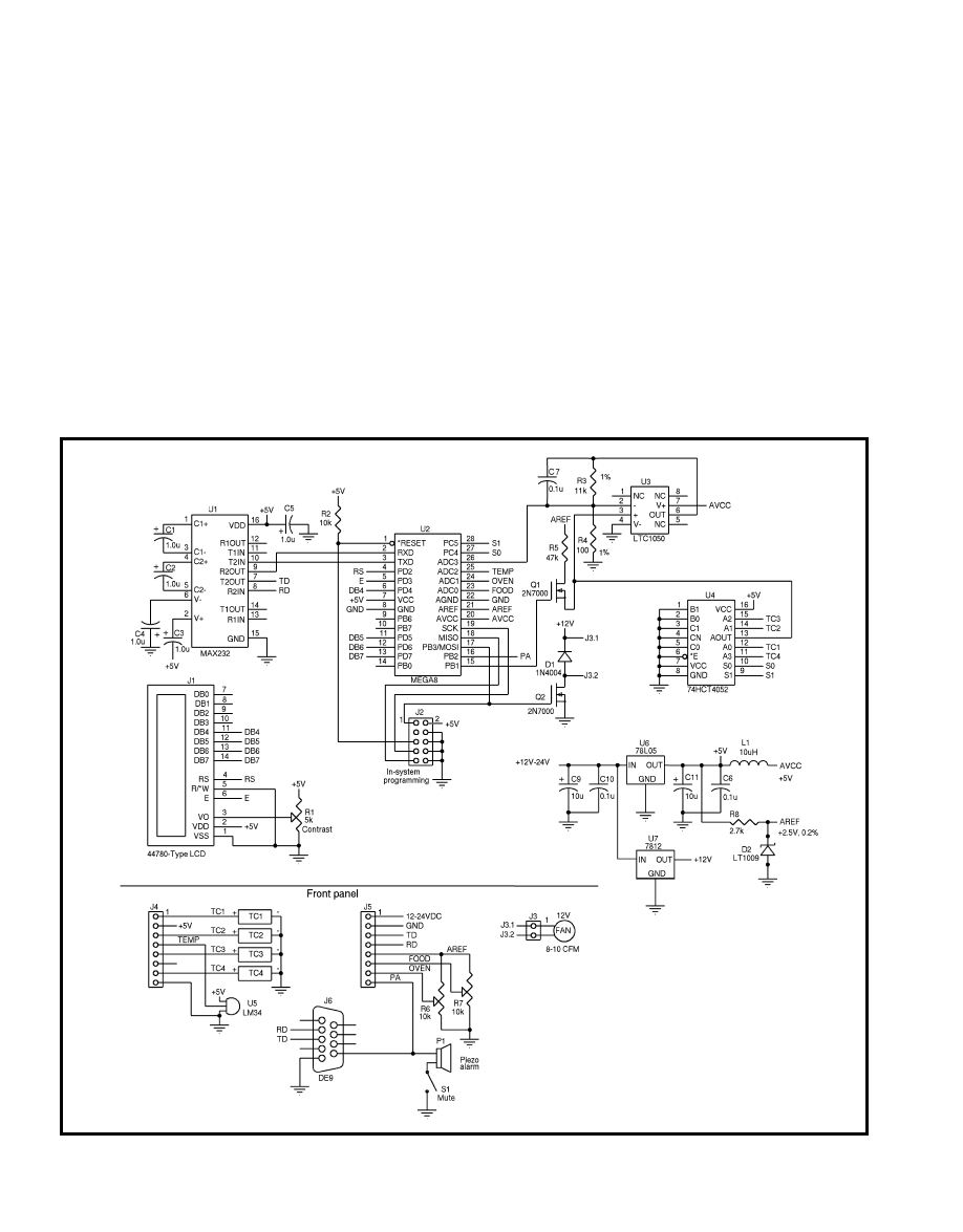
www.circuitcellar.com
CIRCUIT CELLAR
®
Issue 154 May 2003
29
tion is heated, a voltage proportional
to the temperature can be measured at
the other end of the wires. Different
types of metals have been standard-
ized, and their voltage-versus-temper-
ature properties characterized. This
project uses a type-K thermocouple.
Generally, type-K can be used for
temperatures up to 2300°F, although
the insulating materials used in the
low-cost probes limit the upper tem-
perature to approximately 500°F for
Teflon and 900° for glass braid.
Photo 3 shows typical thermocouple
configurations. Although thermocou-
ples are simple, rugged, and inexpen-
sive, they have some properties that
must be accommodated.
Being microprocessor controlled, I
thought it would be easy to add other
functionality, such as additional probes
to monitor the food temperature, and
another control to indicate the desired
final food temperature. An alarm could
ring when the food reached a desired
temperature or if an error condition
occurred. An RS-232 port would allow
cooker and food temperatures to be
logged, either to a local computer or
perhaps a web site for remote access.
Photo 2 shows the front panel of my
final controller implementation.
As for the control system’s accuracy,
my intention was make it at least as
good as a kitchen oven. Temperature
tolerances only needed to be within
±
5°, because barbequing is more of an
art than a science. Temperature is just
one factor to be consider when you’re
trying to determine if the food is
ready to be taken off the fire.
TEMPERATURE ACQUISITION
Temperatures are measured by tak-
ing an analog measurement from a
temperature probe. Converting it to a
digital value using the micro’s A/D
converter, and then converting the
raw measurement to an actual tem-
perature achieves this.
The temperature probe I used is a
thermocouple, which is constructed
simply by connecting two dissimilar
types of metal wire. When this junc-
Figure 2—
The goal is to build a system that is comparable to or better than a kitchen oven. Atmel’s ATmega8 microcontroller is at the heart of the controller.
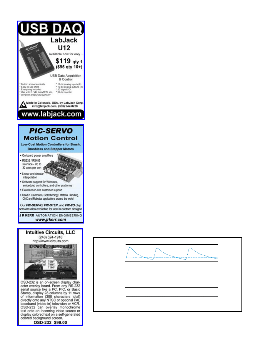
30
Issue 154 May 2003
CIRCUIT CELLAR
®
www.circuitcellar.com
THERMOCOUPLE PROPERTIES
First, the output voltage of a type-K
thermocouple is only about 20 µV (i.e.,
0.00002 V) per 1°F. This must be ampli-
fied in order to use the microprocessor’s
A/D converter, but most amplifiers
aren’t suitable. General-purpose op-
amps typically have input offset voltage
errors of 1 to 5 mV, which corresponds
to a temperature error of hundreds of
degrees! The precision op-amp used
instead has a maximum offset voltage
error of only 5 µV, or less than a quar-
ter-degree error. The amplifier circuit is
configured for a gain of 111; therefore,
by using a 2.5-V reference with the A/D
converter, you can measure tempera-
tures from 32° to roughly 1000°F with
approximately 1° resolution.
Of course, if you were to amplify
the thermocouple signal, you’d also
amplify any noise signals in this not
too carefully constructed circuit. You
can minimize the effects of noise by
taking multiple (32 to 256) A/D read-
ings and averaging them to produce a
single temperature measurement.
The second thermocouple problem
is that output is nonlinear. You cannot
perform a simple division to convert
voltage to temperature. This is easily
dealt with by storing the type-K volt-
age-to-temperature table in the con-
troller software. [1] The 0° to 1000°F
temperature range can be divided into
approximately linear regions. You can
use linear interpolation to determine a
temperature within a given region.
The final thermocouple problem is
that output is relative, not absolute.
The voltage at the probe end of the
thermocouple where the two dissimi-
lar wires connect is relative to the
voltage at the circuit end, where the
thermocouple wires connect to the
voltage measurement circuit. If the
probe and circuit ends have the same
temperature, the measured voltage
will be zero. If the probe end is hot-
ter, a positive voltage will be meas-
ured. If it’s colder, a negative voltage
will be measured.
Therefore, in order to know the
actual temperature at the probe end,
you need to know the temperature of
the circuit end. Historically, this was
accomplished by keeping the circuit
end in an ice bath so its temperature
remained 32°. Consequently, the
connection between the thermocou-
ple and measuring circuit came to be
known as the “cold junction.” The
process of using the junction temper-
ature to calculate the actual probe
temperature is referred to as cold
junction compensation.
Instead of using ice, which is some-
what impractical for a barbecue appli-
cation, you can use an IC temperature
sensor to directly measure the actual
temperature of the cold junction. For
this to work, the sensor and physical
connection point where the thermo-
couple wires meet the copper circuit
wires must be the same temperature
(i.e., isothermal). A difference in tem-
perature will directly affect the accu-
racy of the temperature measurement.
One method, which seems to work
acceptably well, is shown in Photo 4.
0
50
100
150
200
250
300
1
155
309
463
617
771
925
1079
1233
1387
1541
1695
1849
2003
2157
2311
2465
2619
2773
Seconds
T
emp
erat
ur
e
Figure 3—
Compare the temperature values over a 45-min. period for an indoor kitchen oven (dark blue) and the
automatically controlled ceramic cooker (light blue). In this instance, both are set at 225°. As you can see, the
ceramic cooker shows much smaller temperature swings and a more accurate average temperature.
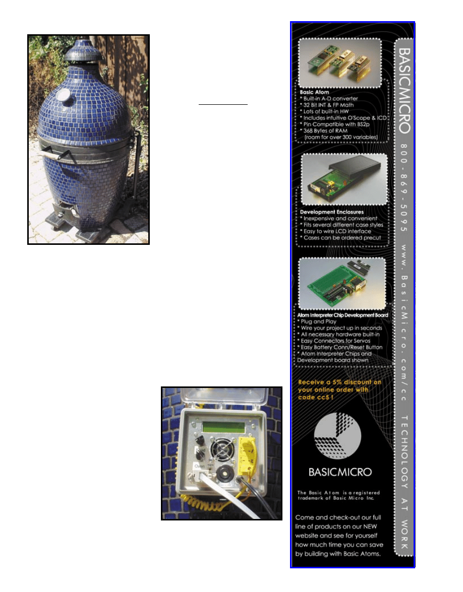
www.circuitcellar.com
CIRCUIT CELLAR
®
Issue 154 May 2003
31
MULTIPLE THERMOCOUPLES
After you have the basic setup to
measure one channel, it’s easy to add an
analog multiplexer to select from one of
several channels. However, in order to
prevent false alarms from the alarm cir-
cuit, you need to know if a thermocou-
ple is actually connected to a channel.
The circuit shown in Figure 1 allows
the microprocessor to determine this.
TEMP MEASUREMENT
You must complete several steps to
make a single temperature measure-
ment. First, select the channel to be
read by setting the analog multiplexer
to one of the four thermocouples. Then,
see if there is actually a thermocouple
connected by turning on the missing
thermocouple test voltage and taking
an ADC measurement. Remember that
a single measurement is actually the
average of 32 to 256 readings.
If the result is the maximum A/D
value, then there is no thermocouple
connected to that channel, so report a
temperature value of zero. Otherwise,
turn off the missing thermocouple test
voltage, and measure the actual ther-
mocouple output.
Using the A/D reading, the amplifi-
er gain (111), and the A/D voltage ref-
erence value (2.5 V), compute the
actual thermocouple voltage. A 10-bit
A/D reading will be in the 0- to 1023-V
range, so the actual voltage is equal to
the following:
Next, take and average multiple
A/D readings of the cold junction tem-
perature sensor, and convert that volt-
age to the cold junction temperature.
Using the cold junction temperature
and the type-K voltage/temperature
table, compute the type-K voltage
that’s equivalent to the cold junction
temperature. Add the thermocouple
voltage to the cold junction voltage.
Using the type-K table, convert the
summed thermocouple and cold junc-
tion voltages to the actual thermocou-
ple temperature.
MEASUREMENT ACCURACY
There are several sources for error in
this process, including the inherent
inaccuracies of the thermocouple and
cold-junction temperature sensor, how
isothermal the cold junction and sen-
sor really are, the accuracies of the
A/D converter and voltage reference,
and gain errors in the amplifier. A
good reality check is to test the tem-
perature of boiling water, because
212°F is actually within the range of
the typical barbecue-cooking tempera-
A/D reading 2.5
111
×
×
1024
Photo 1—
The door at the bottom opens and closes,
and the cap at the top turns to regulate the cooker tem-
perature, which is monitored with a dial thermometer.
Photo 2—
The LCD shows the actual and desired cook-
er temperatures, and up to three food temperatures.
You can mute the piezoelectric alarm. The cooker tem-
perature can be set from 180° to 400°F in 5° steps,
and the food alarm can be set from 100° to 220°F.
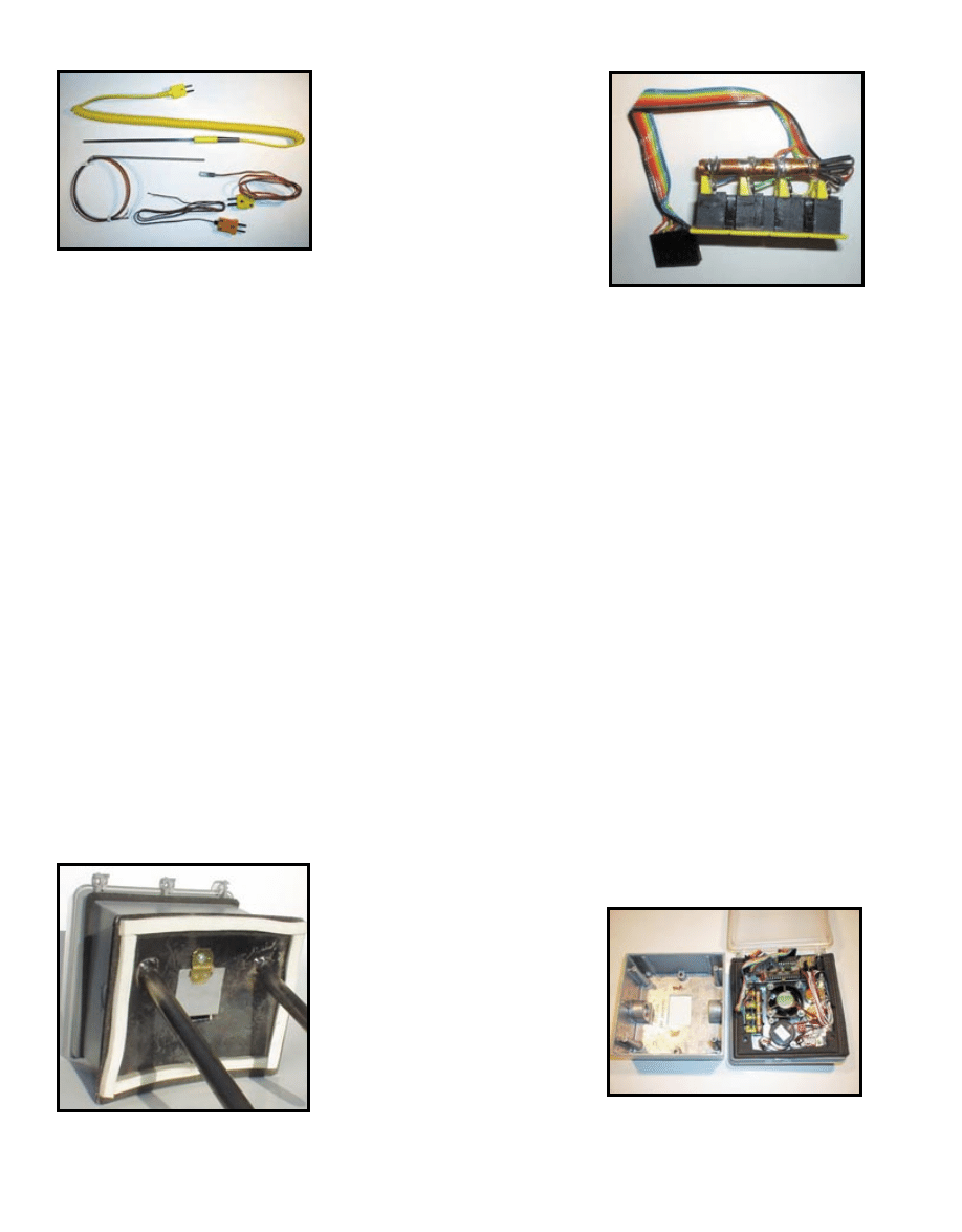
32
Issue 154 May 2003
CIRCUIT CELLAR
®
www.circuitcellar.com
upper draft openings to regulate the
airflow would require a motorized
mechanism. A simpler approach is to
use a small fan.
Little airflow is required for barbecue-
cooking temperatures. The 40-mm fan
that I used only puts out 10 cubic feet
per minute, but can produce cooker
temperatures higher than 400°F.
Although bigger fans can produce
higher temperatures, they’re unneces-
sary for barbequing, and you don’t
want to cook the electronics, which
are mounted only a few inches from
the firebox. The fan speed can be con-
trolled by the microprocessor using
one of its PWM outputs from fully on
to off in 255 steps.
So little airflow is needed that air
leaks can prevent low temperatures
from being reached! There must be a
good seal between the cooker’s lid and
base. Also, you must prevent air from
leaking in through the opening when
the fan is off. The simple flapper valve,
which is shown in Photo 5, accom-
plishes this; it’s constructed from a
piece of aluminum pie pan that’s
epoxy-glued to a small metal hinge.
When the fan is on, it opens the alu-
minum flap. The flap shuts when the
fan is off, sealing the opening.
CONTROLLER ELECTRONICS
Figure 2 shows the schematic for
the controller. The microprocessor is
an ATmega8, which has 8 KB of flash
memory for program storage and 1 KB
of RAM. The on-board oscillator is
used at its default setting of 1 MHz,
so a crystal or clock circuit isn’t
needed. Four of its six A/D channels
are used for the thermocouple ampli-
fier output, LM34 temperature sen-
sor, and potentiometers needed for
the cooker and food temperature set-
tings. Digital lines are used for the
LCD, which has an HD44780-type
interface, fan, analog multiplexer
channel select, piezoelectric alarm,
missing thermocouple detection cir-
cuit, and RS-232 connections.
The ATmega8 can be in-circuit pro-
grammed. Power is supplied through
an unregulated 12-V wall wart or 12-V
sealed lead-acid battery. Regulators are
needed to convert this to 5 V for the
electronics, a 2.5-V 0.2% precision ref-
erence voltage, and 12 V for the fan.
The transistor that controls the fan
must be rated according to the fan’s
current requirements. The fan that I
used draws 100 mA, so a 2N7000
MOSFET that can handle 200 mA is
adequate. With a backlit LCD and the
fan turned on, the current draw is
only 120 mA, so a 7-Ah battery can
power the controller for several days.
The RS-232 port is used primarily
for data logging. Because the barbecue
is usually outdoors and the computer
indoors, a MAX232 and low data rate
(i.e., 2400 bps) are used to allow for
the greatest possible distance between
the controller and data logger. Using
six-conductor telephone cable with
RJ11 to RS-232 modular connectors,
distances of 100
′
are easily achieved.
The alarm signal is also brought out
on the RS-232 cable, so the outdoor
on-board alarm can be muted at night,
and a smaller piezo alarm that’s con-
nected to the end of the cable can be
placed indoors where someone is like-
ly to hear it.
tures. The circuit and setup described
here yielded a boiling water tempera-
ture of 213°F, which is good enough
for barbecue purposes.
DESIGN LIMITATION
The circuit has a design limitation.
When the thermocouple probe is at a
lower temperature than the cold junc-
tion, the voltage produced is negative.
However, the circuit, as configured, is
single-ended, so it treats a negative
voltage as if it were 0 V.
Consequently, if the probe is colder
than the cold junction, the computed
temperature will be the cold junction
temperature, not the actual probe tem-
perature. There are several ways to cor-
rect this, but none were used, because
I was only concerned with high tem-
peratures, not low ones.
AIRFLOW CONTROL
Now you’re capable of measuring
the cooker’s temperature, but how can
you control it? Adjusting the lower or
Photo 6—
The electronics are assembled on a piece of
double-plane prototype board and mounted over the
LCD. The weatherproof gasket and cover come with
the electrical box.
Photo 5—
You don’t want the fire to go out completely;
therefore, when shut, the valve limits but doesn’t com-
pletely restrict airflow through the fan’s opening.
Photo 4—
An LM34 (inside the 0.25
″
copper tube)
measures the tube’s temperature, which is approxi-
mately isothermal with the thermocouple connector.
Photo 3—
Beaded-type thermocouples respond too
quickly for use in an oven. Adding a washer provides
thermal mass. The slender stainless probes are used
for food temperatures. The thicker probe is for oven
temperatures.
HC08 Q FAMILY OF 8-BIT MICROCONTROLLERS
MOTOROLA
and
the
Stylized
M
Logo
are
registered
in
the
U.S.
Patent
and
Trademark
Office.
All
other
product
or
service
names
are
the
property
of
their
respective
owners.
©
Motorola,
Inc.
2002.
• 1.5K–4K of second-generation .5 micron Flash
• 128 bytes of RAM
• Up to 4-ch 8-bit A to D converter
• 2-ch 16-bit timer with input capture, output compare, or PWM
• Trimmable internal OSC (+/-5% accuracy)
• Available in 8-pin DIP/SOIC or 16-pin DIP/SOIC/TSSOP
• 68HC908QT4 demonstration board and tutorial
– CodeWarrior
®
Integrated Development Environment
– C compiler, assembler, linker and debugger
– Auto code generator for on-chip peripherals
– Full chip simulation and Flash programming
HC08 Q FAMILY KEY FEATURES
Efficient. Programmable. Affordable.
Our powerful HC08 Q family of 8-bit micro-
controllers includes six new derivatives,
available now, in volume, and competitively
priced against 8-bit MCUs without Flash.
Available in small 8- and 16-pin packaging
with a full set of peripheral options – and
more are in development. Leading edge
Motorola Flash is easier to program and
is re-programmable in
the field, so products
are “Future Enabled”
to stay in the market longer. Get started for just $25 with the comprehensive
68HC908QT4 Demonstration Kit. Order yours now at www.motorola.com/mcu
JUST WHAT 8-PIN MCUs NEED:
A LITTLE FLASH
.
System Integration Module
External Interrupt
Power-On-Reset
Low-Voltage Inhibit
MON08
COP
Internal RC
128 Bytes RAM
HC08
CORE
2 Channel
16-Bit Timer
• Input Capture
• Output Compare
• Pulse Width Mod.
4K Bytes
FLASH
1.5K Bytes Option
4 Channel
8-Bit ADC
I/
O
Demonstration Kit
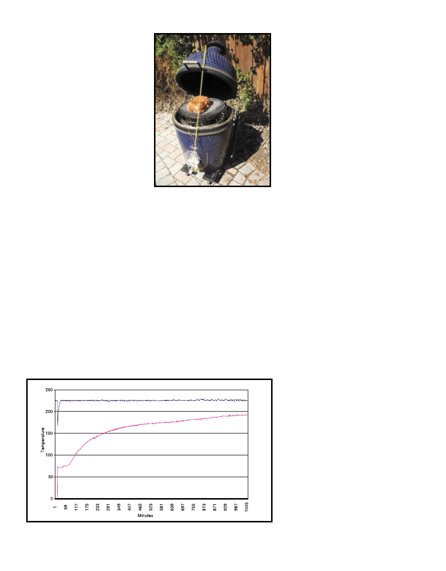
34
Issue 154 May 2003
CIRCUIT CELLAR
®
www.circuitcellar.com
Photo 6 shows the electronics,
which are mounted on the lid of a
standard doublewide outdoor “wet
location” electrical box. The box itself
is mounted to the lower draft door of
the cooker. The cover supplied with
the box allows the controller to stay
outdoors and mounted on the cooker
at all times. Alternate packaging
schemes are possible, such as mount-
ing the fan on the draft door, with the
electronics further away in a separate
box. Or you could choose to mount
nothing on the cooker itself and pipe
the air to the cooker through a metal
pipe or flex tubing.
CONTROLLER SOFTWARE
The software was written with the
ImageCraft ICCAVR C compiler.
Approximately half of the 8 KB of
flash memory has been used so far.
The ATmega8’s flash memory is in-
circuit programmed through an Atmel
standard ISP header. The ImageCraft
IDE provides a programmer. In addi-
tion, stand-alone programming soft-
ware is widely available on the
Internet. ImageCraft also offers a free
30-day unrestricted trial period for its
IDE and compiler.
The software continuously reads the
thermocouple temperatures, cooker,
and alarm settings, and then displays
them on the LCD. The alarm is
sounded if there is no cooker tempera-
ture probe, the cooker temperature is
too high or too low, or the tempera-
ture of the food has reached the alarm
temperature. A simple software state
machine is used to prevent “temp too
low” alarms during the time the
cooker is coming up to temperature,
set-point changes, and when the lid is
opened during cooking. The settings
and temperature readings are sent to
the RS-232 port once per second so
that a terminal capture program, such
as HyperTerminal, can be used for
data logging.
The temperature reading and set-
tings are used to implement the con-
troller’s main function (i.e., the
process-control algorithm). Once per
second, the desired and actual cooker
temperatures are used to determine
the fan’s speed. Note that the con-
troller was designed with two control
strategies in mind, On/Off and PID.
ON/OFF CONTROL
If the cooker temperature is below
the desired level, the simplest control
algorithm is to turn on the fan fully.
Turn it off if the cooker temperature
is above the desired value. The result-
ing cooker temperature will tend to
oscillate around the desired value,
because the thermal inertia in the
cooker will cause the temperature to
continue to rising after the fan is
turned off and falling after the its
turned on. As long as the average tem-
perature is what you want and the
swings aren’t too big, this is perfectly
acceptable. After all, this is how most
kitchen ovens work, and the goal is to
be as good as one of those.
PID CONTROL
A more sophisticated approach is to
set the fan to the exact speed needed
to reach a given temperature, and then
incrementally adjust the speed to
maintain that temperature as condi-
tions change. The PID algorithm uses
proportional, integral, and derivative
calculations to do just that.
A measure of current conditions,
the proportional part of the calcula-
tion is based on the size of the error
(i.e., the difference between the
desired temperature and the actual
temperature). The integral portion of
the calculation is based on the sum
of all the previous error values; it’s a
measure of any longer-term error
trend. The derivative part of the cal-
culation is based on the change in
the error, not the temperature, and it
measures how quickly the error is
changing.
Each of the three components can be
given a different weighting factor. If the
weighting factors are chosen correct-
ly—through a process called “tuning”—
the PID algorithm will adjust the fan
speed to bring the actual temperature to
the desired temperature with no over-
shoot, and it will maintain that temper-
ature with little or no oscillation even if
conditions change. Parallax’s Industrial
Control Student Guide Version 1.1
Figure 4—
The data log shows a stable ceramic cooker temperature (in blue) and a slowly rising meat temperature
(in red). The initial temperature dip occurred when I opened the lid to the preheated cooker to add the food.
Photo 7—
A typical setup includes food, oven and food
temperature probes, and the controller.
www.circuitcellar.com
CIRCUIT CELLAR
®
Issue 154 May 2003
35
provides a straightforward introduc-
tion to the PID algorithm.
Although the hardware was
designed with a variable fan speed so
that PID could be used, I ran the ini-
tial tests with an On/Off algorithm.
The results are shown in Figure 3.
The goal was to build a device that is
as good as an indoor oven. But, even
with a simple On/Off control, the
ceramic cooker is considerably better.
So, the final controller uses On/Off
control, and the more complex PID
algorithm isn’t needed.
USING THE SYSTEM
Photo 7 shows the ceramic cooker
with the automatic temperature con-
troller in a typical setup. The meat,
rubbed with secret barbecue spices, is
on the top grill with a drip pan under-
neath it. Beneath the drip pan is a foil-
covered pizza stone, which prevents
the bottom of the meat from charring.
A full load of hardwood lump charcoal
is under the pizza stone. I added
chunks of hickory and cherry wood to
add a smoked flavor.
After the temperature probes are
inserted and the lump lit, close the
lid. The upper draft control is opened
a half turn, and the cooker tempera-
ture and food alarms are set. As soon
as the alarm sounds, you can check
the meat to see if it’s done. You aren’t
required to monitor or adjust the
cooker temperature, although some
barbecue styles require you to periodi-
cally baste and turn the meat.
Figure 4 shows the log of an actual
cooking session. The meat required
approximately 17 h to reach a final
temperature of 192°F. The cooker tem-
perature was set at 225°F. It stayed
within 3° of that setting more than
98% time, and remained within 1°
more than 85%.
WHO’S TENDING THE FIRE?
Traditionalists may question the
idea that real barbecue can be achieved
without an all-day or all-night fire-
tending vigil. But modern technology
can make this cooking style accessible
to those who otherwise wouldn’t have
the time for it.
The system is useful for more than
barbequing. After the fire is lit, the
cooker is as easy to use as a kitchen
oven but has the advantage of better
temperature control. In addition, it
makes it easy to monitor food tempera-
ture, and it gives you the ability to add a
smoked flavor to anything you cook.
I
SOURCES
ATmega8 Microprocessor
Atmel, Inc.
(408) 441-0311
www.atmel.com
ICCAVR C Compiler
ImageCraft
(650) 493-9326
www.imagecraft.com
LTC1050 Precision op-amp
Linear Technology Corp.
(408) 432-1900
www.linear.com
Type-K Thermocouple
Omega Engineering, Inc.
(203) 359-1660
www.omega.com
PROJECT FILES
To download the code, go to
ftp.circuitcellar.com/pub/Circuit_
Cellar/2003/154/.
RESOURCES
BBQ information and recipes,
www.eaglequest.com/~bbq/.
Ceramic Cooker, Kamado Corp.,
www.kamado.com.
Parallax, Inc., Industrial Control
Student Guide Version 1.1
, 2001.
REFERENCE
“Revised Thermocouple
Reference Tables,”
www.omega.com/temperature.
John Moyer earned a computer sci-
ence degree from the University of
California, Berkeley. Although John
has experience working on microcon-
troller-based data acquisition and
control products, he’s currently
focused on developing shrink-
wrapped Mac and Windows graphics
software. You may reach him at
jmoyer@pacbell.net.

36
Issue 154 May 2003
CIRCUIT CELLAR
®
www.circuitcellar.com
ou can use the
MSP430 ultralow
power, mixed-signal
processor to perform the
real-time signal processing necessary to
implement a dual-tone multifrequency
(DTMF) decoding application. The
DTMF-controlled remote switching sys-
tem—the construction and function of
which is discussed in this article—con-
nects to an ordinary analog telephone
line in parallel with a user phone. It
allows you to control eight electric
switches by making a call to the phone
attached to the MSP430 device. By
punching in an access code and simple
instruction sequence, you can turn on
or off any of the eight lines. In other
words, you can remotely control your
lawn sprinklers, air conditioner, and
house lights if they’re connected to one
of the telephone-controlled switching
outputs on the MSP430 application.
To build an application like this,
you need hardware to form the inter-
face between the telephone line and
MSP430 microcontroller. In addition,
you need signal-processing capabili-
ties—which are provided by the
MSP430 and used for deciphering infor-
mation encoded as electrical signals on
the telephone line—and a control pro-
gram for the MSP430.
DECODING DTMF
DTMF is a scheme for encoding
16 characters using the sums of sinu-
soidal signals of two distinct harmoni-
cally unrelated frequencies. Table 1
shows how each of the 16 characters
is represented. One frequency is from
a low-frequency group (i.e., ranging
from 697 to 941 Hz), and one is from a
high-frequency group (i.e., ranging
from 1209 to 1633 Hz).
DTMF is widely used in telecommu-
nication systems. To transmit a partic-
ular character on a telephone line, the
two frequencies representing that char-
acter are generated as electrical signals,
added, and sent down the line. A speci-
fied period of silence (40 ms or more)
separates one transmitted DTMF char-
acter from another. A receiving device
decodes the character being transmit-
ted by identifying the two frequencies
present in each sum it receives.
To identify the DTMF character
received by the MSP430 application,
the analog voltage signal on the tele-
phone line is sampled. Then, it’s con-
verted to a digital value using the 10-bit
A/D converter (ADC10) peripheral on
the MSP430F1232 chip. A 3640-Hz
sampling frequency is used. This fre-
quency is more than two times the
highest DTMF frequency, and it satis-
fies the Nyquist criterion, which guar-
antees that the integrity of the signal
will be preserved after sampling. The
sampled signal then passes through
each of the eight wave digital filters to
identify which two DTMF frequencies,
if any, are present in the sampled signal.
The digital processing of voltage sig-
nals eliminates the need for additional
circuitry that’s external to the
MSP430 for implementing analog fil-
ters. Wave digital filters are used for
this purpose; they’re implemented in
DTMF-Controlled Remote
Switching System
y
Interested in remotely
controlling your sprin-
klers, house lights,
and air conditioners
with a phone and a
password? In this arti-
cle, Arthur shows you
how to do so by con-
necting his MSP430
microcontroller-based
DTMF-controlled
switching system to a
telephone line.
Arthur Musah
FEATURE
ARTICLE
Frequency (hertz)
1209 1336 1477 1633
697
1
2
3
A
770
4
5
6
B
852
7
8
9
C
941
* or E
0
# or F
D
Table 1—
In the DTMF-encoding scheme, 16 charac-
ters are encoded using eight harmonically unrelated
frequencies.
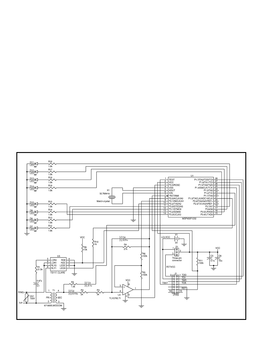
www.circuitcellar.com
CIRCUIT CELLAR
®
Issue 154 May 2003
37
(R1) into the ring-detect portion of U3.
When there’s no ring signal on the
phone line, the ring-detect output
maintains a logic-high value. A logic-
low value on the output indicates the
detection of a telephone ring. The
ring-detect output of U3 is connected
to an MSP430 I/O pin (i.e., pin 10) to
generate an interrupt to the MSP430
on each telephone ring.
Regarding the hookswitch, a dedi-
cated I/O pin (i.e., pin 21) on the
MSP430 is connected to the relay
control pin of U3. It’s used to turn
the solid-state relay portion of U3 on
or off, and to close or open the cir-
cuit on the primary side of the trans-
former T1.
The DTMF input line comprises the
secondary side of the transformer (T1);
it feeds into the op-amp input and
from the op-amp output to pin 8
(ADC channel A0) of the MSP430.
software and have desirable features
such as response stability and good
dynamic range.
A DTMF-decoding algorithm for the
MSP430 makes use of eight wave digi-
tal filters, which are conveniently
implemented with shift-and-add mul-
tiplications to circumvent the need for
a hardware multiplier. [1] Each filter is
designed to have a resonant frequency
corresponding to one of the DTMF fre-
quencies. Thus, a signal whose fre-
quency matches the resonant frequen-
cy of the filter it passes through will
be magnified by a known factor char-
acteristic to the filter. At the same
time, the noise and signals of the
other frequencies will be significantly
attenuated. Then, the output of a fil-
ter can be analyzed to determine if a
particular frequency was present in a
signal. If you want to learn more
about wave digital filtering for the
MSP430, you’ll find the references and
resources at the end of this article to
be extremely helpful.
HARDWARE
The schematic in Figure 1 shows
the hardware that interfaces the tip
and ring telephone lines with the
MSP430, JTAG interface, and eight
LEDs used for demonstrating the
application’s switching action. Note
that the interface between the phone
line and MSP430 consists of four func-
tional parts: ring detection, the hook-
switch, a DTMF input line, and a
notification tone output line.
U3 combines the ring-detection
function and a solid-state relay for
implementing the telephone hook-
switch in one IC. The capacitor C1
DC-filters the 15-Hz ring signal from
the telephone line, which then passes
through the current-limiting resistor
Figure 1—
The MSP430 implements the digital filtering and application control. One IC (U3) performs ring detection and hookswitching, while the transformer isolates the appli-
cation from the telephone line. Eight LEDs are used to display the switching action of the application.
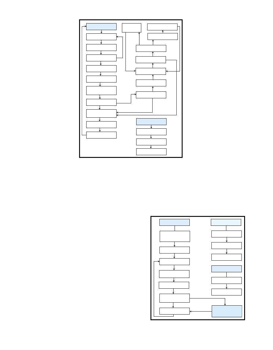
38
Issue 154 May 2003
CIRCUIT CELLAR
®
www.circuitcellar.com
Because DTMF signals are
AC signals, they’re propagat-
ed from the telephone line on
the primary side of T1 to the
secondary side. The signal
path through R8 and C3 to
pin 23 of the MSP430 is
blocked to DTMF signals by
placing I/O pin 23 in High-
Impedance mode when
receiving DTMF. Therefore,
DTMF signals pass through
the DC-filtering capacitor,
C2, and are amplified by U4
and sampled at pin 8 of the
MSP430. The op-amp U4 also
biases the amplified DTMF
signals at V
CC
/2 to enable the
A/D converter to convert
samples from the upper and
the lower half cycles of the
sinusoidal signal.
The notification tone out-
put line is the path for square-
wave signals generated as user
notification tones by the
MSP430 Timer_A peripheral.
Driving the shutdown pin on
the op-amp low shuts down
the op-amp U4; the op-amp outputs
are placed in High-Impedance mode
when a user notification tone is out-
put. The square wave goes through
C3, R8, and the secondary side of T1;
it’s propagated to the primary side and
the telephone line, which transmits it
to the user’s earpiece.
The JTAG interface provides the
appropriate signal connections for in-
system programming the MSP430 via
a PC parallel port. [2] The jumper
switch S1 provides the option of pow-
ering the board from either the on-
board battery (V1) or a PC connected
via the JTAG interface.
The eight LEDs—D7 to D14—are
connected to MSP430 output pins
through current-limiting resistors,
R12 to R19. The MSP430 can turn
them on or off to demonstrate the
switching function of the application
(see Photo 1).
CONTROL THE MSP430
The MSP430 CPU runs at a fre-
quency between 4.4 and 5.4 MHz by
setting the on-chip digitally con-
trolled oscillator (DCO) to run at the
maximum settings. [3] This CPU fre-
quency is adequate for the application,
because the sampling frequency is
obtained from a more precise 32,768-
Hz ACLK signal. The flowchart in
Figure 2 depicts the flow of the main
control program for the
DTMF-controlled remote
switching application.
Counter variables are
cleared, and the CPU is
turned off to wait for ring
interrupts. A ring counter
is incremented in the ring
interrupt service routine.
Most standard ring
cadences have a 6-s period.
(This application was test-
ed with a typical U.S. ring
cadence of 2 s on and 4 s
off.) The return from the
ring interrupt service rou-
tine (inside of which ring
interrupts are disabled) is
delayed for 4 s using the
watchdog timer available
on the MSP430. This delay
ensures that a single ring
is not counted multiple
times because of a fluctuat-
ing ring detect signal with
multiple falling edges caus-
ing multiple ring interrupts
to be generated.
Ring signals are counted
until the specified number is
obtained (i.e., five in this
implementation). The appli-
cation then seizes the tele-
phone line and confirms this
to the user with a tone. The
user has one chance to enter
a correct password, and if
there is a password match,
the application runs in
Switch mode, where it
accepts and executes valid
DTMF signals representing
switch actions requested.
On the demonstration
board, eight LEDs are turned
on or off to show the switch-
ing action. In a real-world
product, the eight outputs can
be used to turn low-current
solid-state relays to turn iso-
lated circuits on or off.
DTMF DECODING ALGORITHM
Timer_A triggers the A/D converter
on the MSP430 to sample the voltage
level on channel A0 at intervals of
274.7 µs. In the time between two
samples, the current sample is used to
Reset
Initialize system
CPU in LPM
Ring counter greater
than or equal to five?
N
Seize phone line
Y
Confirmation tone
Decode DTMF in
Password mode
Termination character
decoded?
Clear variables
Clear input storage
Error/Hang-up tone
Hang-up phone line
N
Y
Error/Hang-up
tone
Confirmation tone
Perform switch action
Switch commad
valid?
N
Y
Termination
character decoded?
Decode DTMF in
Switch mode
N
Y
Confirmation tone
Password correct?
N
Y
RING_ISR
Increment ring
counter
4-s delay
RETI
Figure 2—
This flowchart should help you understand the control program for
the DTMF-controlled switching application.
DTMF Decode
Initialize ADC10 and
Timer_A for sampling at
3640 Hz
CPU in LPM
Fetch sampling value
from ADC10
Calculate eight
digital filters
Store filter values
Count sample runs
Enough filter runs
calculated?
CPU in LPM to wait
for next sample
N
CCR0_ISR
Start A/D
conversion
Increment time
out counter
RETI
ADC10_ISR
Start calculation
in Active mode
RETI
Y
Recognition of DTMF
signal from calculated
filter values
Figure 3—
Study the algorithm for decoding DTMF. Timer_A interrupts
are used to implement the 3640-Hz sampling frequency of the ADC.
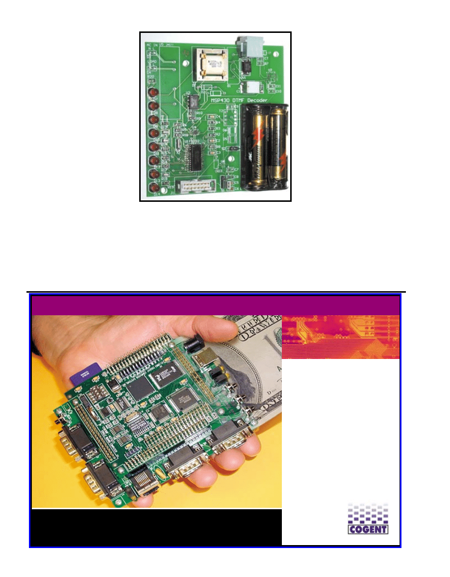
www.circuitcellar.com
CIRCUIT CELLAR
®
Issue 154 May 2003
39
calculate the eight filter outputs
to identify two maximum values
from the high- and low-frequen-
cy groups in the DTMF table.
Twenty filtering cycles are car-
ried out to allow all of the filters
to reach a steady state and the
various frequencies to go
through their peak amplitudes.
Twenty cycles correspond to
20 × 0.2747 ms = 5.494 ms,
which is longer than the longest
DTMF signal period of 1.435 ms
for the 697-Hz wave.
After consolidating these
20 samples, a check is performed
to determine if the two maximum
filter output values are above the
natural noise level. Another check
is performed to make sure that
the difference between the two
values is not excessive.
Each time a valid DTMF frequency
combination is identified, a signal
length counter is incremented until
the required signal length is reached.
This means eight iterations of this
procedure are required to ensure that
length counter is decremented.
The DTMF flag is cleared when
the signal length reaches zero,
and this indicates a valid pause
between DTMF characters.
Figures 3 and 4 graphically
describe the DTMF decoding
algorithm. For an in-depth
description of the DTMF decod-
ing algorithm for the MSP430,
refer to Robert Siwy’s
Generation and Recognition of
DTMF Signals with the
Microcontroller MSP430
.
IMPLEMENT COMMANDS
Before calling the DTMF-
decoding subroutine in the main
control program, an operation
mode is selected with a mode
control flag. This selects the
number of DTMF characters to
decode and save in memory before
returning from the subroutine.
In Password mode, a sequence of
four password characters is stored.
This is compared to the software-pro-
grammed password upon exiting the
the 40-ms, must-recognize DTMF
specification is met. A flag is set
when a DTMF tone of appropriate
length is identified.
If a DTMF tone isn’t recognized
after a set of 20 filter runs, the signal
Photo 1—
The DTMF-decoding circuit board can be used to turn on or
off eight LEDs over a telephone line. Two AA cells power it.
Time Is Money – Cut Your Development Time For Under $300
Or for more information, call 401-295-6505 or email
files and schematics as well as custom versions are also available.
deliver to embedded system developers.
Our Cogent SBC’s give you everything you
• 2 CAN Ports connect you to the most
popular industrial application bus.
• SD/MMC Card gives you access to
additional FLASH, Bluetooth and 802.11
• Real-Time Clock with battery backup
• Compatibility with standard prototyping
boards (All headers on .1 inch grid)
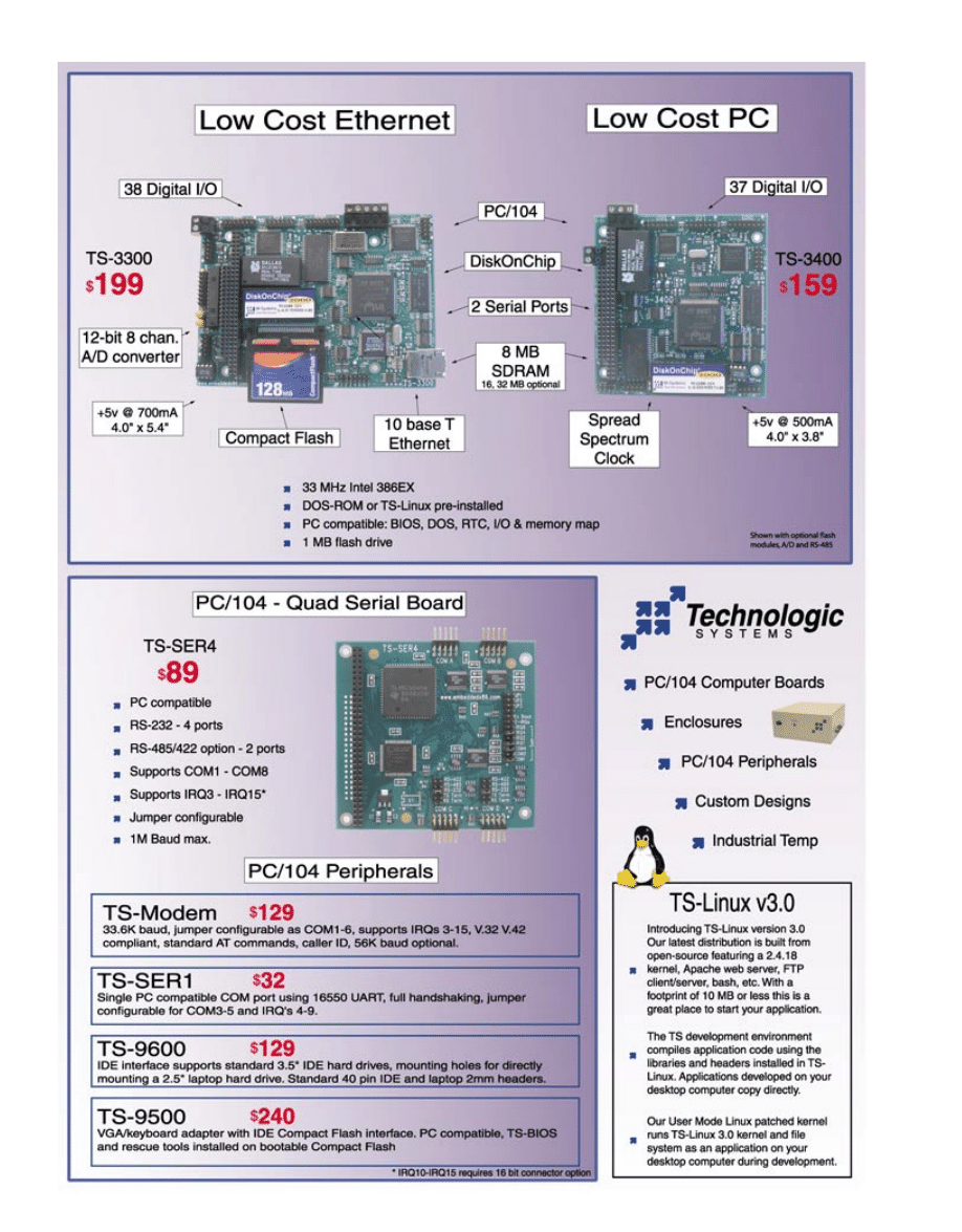

42
Issue 154 May 2003
CIRCUIT CELLAR
®
www.circuitcellar.com
decoding subroutine. (The password
length was specified as four in the
demonstration program, but it can be
changed in the software.)
In Switching mode, the decoding
subroutine returns after saving a
sequence of two DTMF characters.
The first character should be within
the range zero through seven to indi-
cate which line is to be switched. A
valid second character in Switch mode
is either a zero (i.e., to switch off the
selected line) or a one (i.e., to switch on
the selected line). In either mode, the
identification of the DTMF character,
or termination character (* or E), results
in the abrupt termination of the DTMF
decoding subroutine. The character is
stored at the start of the decoded DTMF
sequence before returning to indicate to
the calling program that a hang up/ter-
mination request was received.
TIMEOUT FUNCTION
The telephone-controlled switch
application hangs up after 8 s of not
receiving DTMF tones. To implement
this function, a timeout counter is
incremented each time the Timer_A
signals the ADC10 to start a new sam-
ple. This means that the timeout count-
er is incremented every 0.2747 ms, and
the function can be implemented by
executing the timeout action when
the counter reaches a value of 29,120
(29,120 × 0.0002747 s = 7.999 s).
The idle-time timeout counter is
cleared every time a new DTMF char-
acter is recognized. After a DTMF
decoding cycle of 20 filter calcula-
tions, the timeout counter is com-
pared to the timeout value. If the
timeout value is reached, the termina-
tion character (* or E) is stored at the
beginning of the decoded DTMF
sequence in the memory and DTMF
decoding ceases. The control program
checks for this character when the
DTMF decoding subroutine returns.
AUDIBLE TONE GENERATION
Notification tones are used to pro-
vide feedback about the status of the
DTMF decoder application. Two dis-
tinct notification tones within the
human audible frequency range (20 to
20,000 Hz) are produced by the
MSP430. The higher frequency tone is
the confirmation tone, which is used
for off-hook notification and to indi-
cate that user input (e.g., a password
or switch command sequence) is valid.
The lower frequency tone is the error
tone, which indicates that invalid user
input was received. It’s also the hang-
up (on-hook) notification tone.
Timer_A on the MSP430 chip is used
to output a square wave of a selected
frequency on P1.2 placed in the output
direction (see Figure 5). This square
wave is DC-filtered through capacitor
C3 and passed through the secondary
side of the transformer (T1). (Note that
the op-amp is shut down and its out-
puts are placed in High-Impedance
mode during this process.) The signal
appears on the primary side and is
transmitted on the phone line to an
earpiece where it’s converted into a
sound wave of the specified frequency.
The 32,768-Hz auxiliary clock signal
(ACLK) is selected for the Timer_A
clock. To generate the higher-frequen-
cy square wave (512 Hz), Timer_A
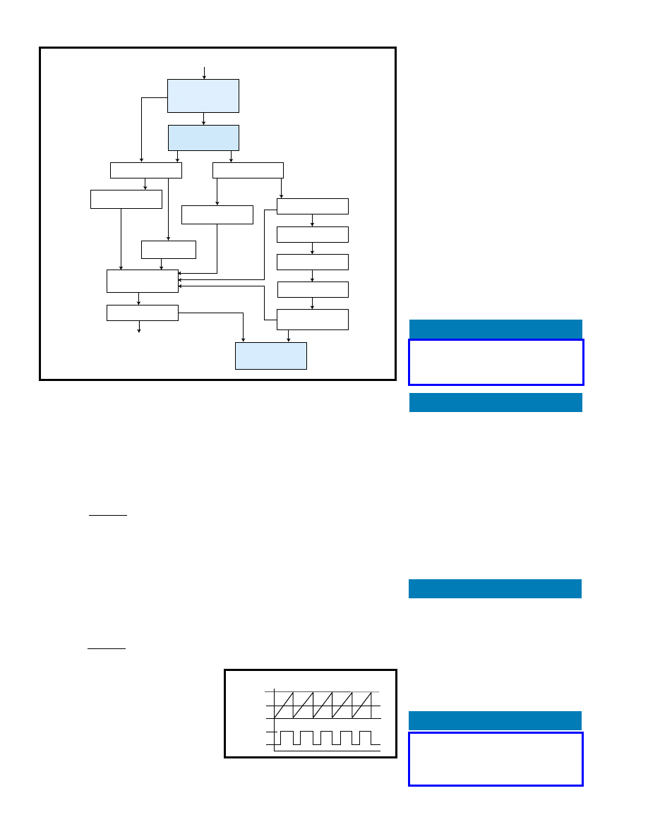
counts from zero to 63 and then starts
again from zero (i.e., 64 clock cycles).
The output is set to a logic-high level
on the thirty-second count and reset
to a logic-low level on the sixty-fourth
count (i.e., on the 63-to-zero transition):
To generate the lower-frequency
square wave (128 Hz), Timer_A counts
256 cycles of the clock. The output is
set on the one hundred twenty-eighth
count and reset on the two hundred
fifty-sixth count:
The timer is stopped after the wave
has been output for the required
length of time.
USING THE APPLICATION
First, dial the appropriate number
from a phone other than the one to
which the application is connected.
32 768
256
128
,
Hz
Hz
=
32 768
64
512
,
Hz
Hz
=
www.circuitcellar.com
CIRCUIT CELLAR
®
Issue 154 May 2003
43
PROJECT FILES
To download the code and parts
list, go to ftp.circuitcellar.com/
pub/Circuit_Cellar/2003/154/.
Arthur Musah worked with the
MSP430 microcontroller/mixed-signal
processor group at Texas Instruments
in the summer of 2002. Currently,
he’s a junior at the Massachusetts
Institute of Technology, studying
electrical engineering and computer
science. You may reach him at
amusah@mit.edu.
REFERENCES
[1] R. Siwy, Generation and
Recognition of DTMF Signals
with the Microcontroller
MSP430
, Texas Instruments,
Inc., SLAAE16, October 1997.
[2] Texas Instruments, Inc., MSP-
FET430 Flash Emulation Tool
(FET) User’s Guide
, 2001.
[3] ———, MSP430x11x2,
MSP430x12x2 Mixed Signal
Microcontroller Datasheet
,
SLAS361, 2001.
RESOURCES
Texas Instruments, Inc.,
MSP430x1xx Family User’s
Guide
, SLAU049B, 2002.
U. Kaiser, “Wave Digital Filtering
for TI’s Sensor Signal Processor
MSP430,” TI Technical Journal,
November/December 1994.
SOURCE
MSP430 Microcontroller
Texas Instruments, Inc.
(800) 336-5230
www.ti.com
Note that the application responds
after five unanswered rings and sends
a confirmation tone (i.e., a high-
pitched beep).
Next, enter a password (e.g., 1-2-3-4,
or as programmed in software). You’ll
hear the confirmation tone for a pass-
word match. An error tone, which is a
low-pitched beep, occurs after a mis-
match. After you hear the confirma-
tion tone of a password match, enter a
digit between zero and seven to indi-
cate which of the eight lines on the
application you wish to switch.
Following this, you can enter either a
zero to turn off the selected line or a
one to turn on selected line. At that
point, a confirmation tone indicates
that a valid two-digit switch com-
mand was executed. An error tone
indicates an invalid switch command
decoded by the application.
You can cycle through these steps as
many times as necessary. To hang up,
press the star key (*) at any time. Note
that the application sends an error tone
and automatically hangs up after 8 s of
silence (i.e., when a key isn’t pressed
and a DTMF signal isn’t received).
I
X
(X + 1)/2
0
High
Low
Timer_A counter
Square wave output
Figure 5—
Timer_A of the MSP430 microcontroller can
generate a square wave.
Difference between the
two maximum
values excessive?
Signal length equals 0?
Decrement signal
length counter
Clear flag
Clear counter for
filter runs
Process decoded
DTMF character
Timeout counter equals
timeout value?
Signal length
reached?
Increase signal
length counter
Flag set?
Determine place in table
Clear timeout
counter
Stop decoding DTMF
Return
Enough filter runs calculated
Both maximum filter
values above natural
noise levels?
N
Y
N
N
Y
N
Y
Y
N
Set flag
N
Calculate next filter run
Exit
Continue
Y
Y
Figure 4—
The recognition of DTMF comes from calculated filter values.
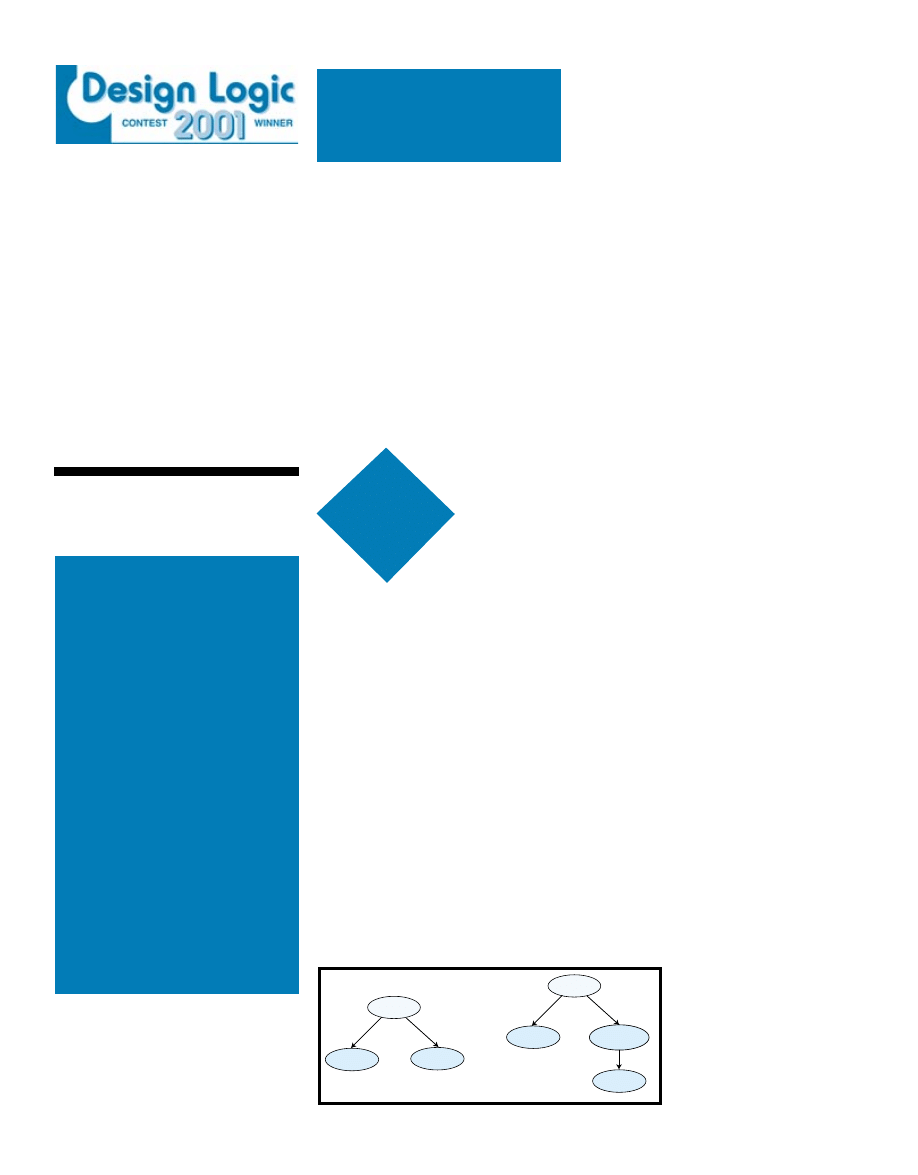
44
Issue 154 May 2003
CIRCUIT CELLAR
®
www.circuitcellar.com
hen designing an
embedded system,
there always comes a
time when you have to
choose a connectivity solution for the
microcontroller. Your options range
from connecting peripheral ICs, to link-
ing a PC or another embedded system.
Many protocols and interfaces are suit-
able for making connections, but if the
connection is between devices rather
than chips, you’ll always end up with
cables, line drivers, and connectors.
This seems to be coming to an end
with the emergence of Bluetooth, a
short-range wireless communications
protocol that’s designed to replace
cables. In fact, Bluetooth is a protocol
stack running on a processor. It pro-
vides wireless support, standardizing
how connections between devices will
be established and destroyed, and how
data will be transmitted between two
or more connected devices.
A Bluetooth connection is achieved
by using dedicated chipsets on both
sides of the communication channel.
These dedicated chipsets usually incor-
porate the radio and baseband proces-
sor, and they handle encoding, modula-
tion, frequency hopping, and all of the
basic processing that’s required for an
information packet to move between
Bluetooth chips.
Blueport was created to interconnect
embedded systems through Bluetooth
when the available Bluetooth modules
include the host controller interface
(HCI) (i.e., there was no higher layer
support built into the Bluetooth mod-
ule). In such circumstances, Bluetooth-
enabling a small embedded system
that’s based on an 8-bit microcontroller
without external RAM and limited
resources proves to be a difficult task,
because the Bluetooth protocol stack
and the application must run on the
micro. Most small microcontrollers
with communications capabilities have
a UART or SPI interface, so the idea
was to use the SPI interface (as hard-
ware or simulated from software) from
the existing system to talk to a stand-
alone module doing all the Bluetooth
stuff. The module is considered an SPI
slave device, so other SPI devices can
be connected to the SPI bus.
The stand-alone module has a simple
API that’s accessible through the SPI.
Encapsulating operations is achieved
over the Bluetooth stack: connect and
disconnect to a Bluetooth device
(including L2CAP channel negotiations)
and then send and receive data from the
connected device. This solution is effi-
cient because the Bluetooth-related pro-
cessing, which is extremely resource
consuming, is handled by a separate
processor. This reduces the load on
the small microcontroller running the
application. Using this approach makes
communication via Bluetooth as sim-
ple as communicating over an SPI (or
Blueport
w
Blueport is a com-
pact, card-sized mod-
ule that you can
implement as a smart
SPI peripheral. By fol-
lowing Zoltan’s lead,
you can achieve
seamless wireless
communication for
your embedded appli-
cations. It’s time to
say goodbye to those
piles of cables.
Zoltan Molnar
FEATURE
ARTICLE
Bluetooth Interface for Embedded
Systems
Figure 1a—
There are two possi-
ble network topologies with
Bluetooth nodes. The master is
the device initiating the connec-
tion between two devices. In a
piconet, a master can have up to
seven slaves.
b—
A scatternet is
a set of piconets interconnected
by nodes simultaneously con-
nected to two different piconets.
Master
Slave 1
Slave 2
Master 1
Slave 1
Slave 2/
Master 2
Slave 3
a)
b)
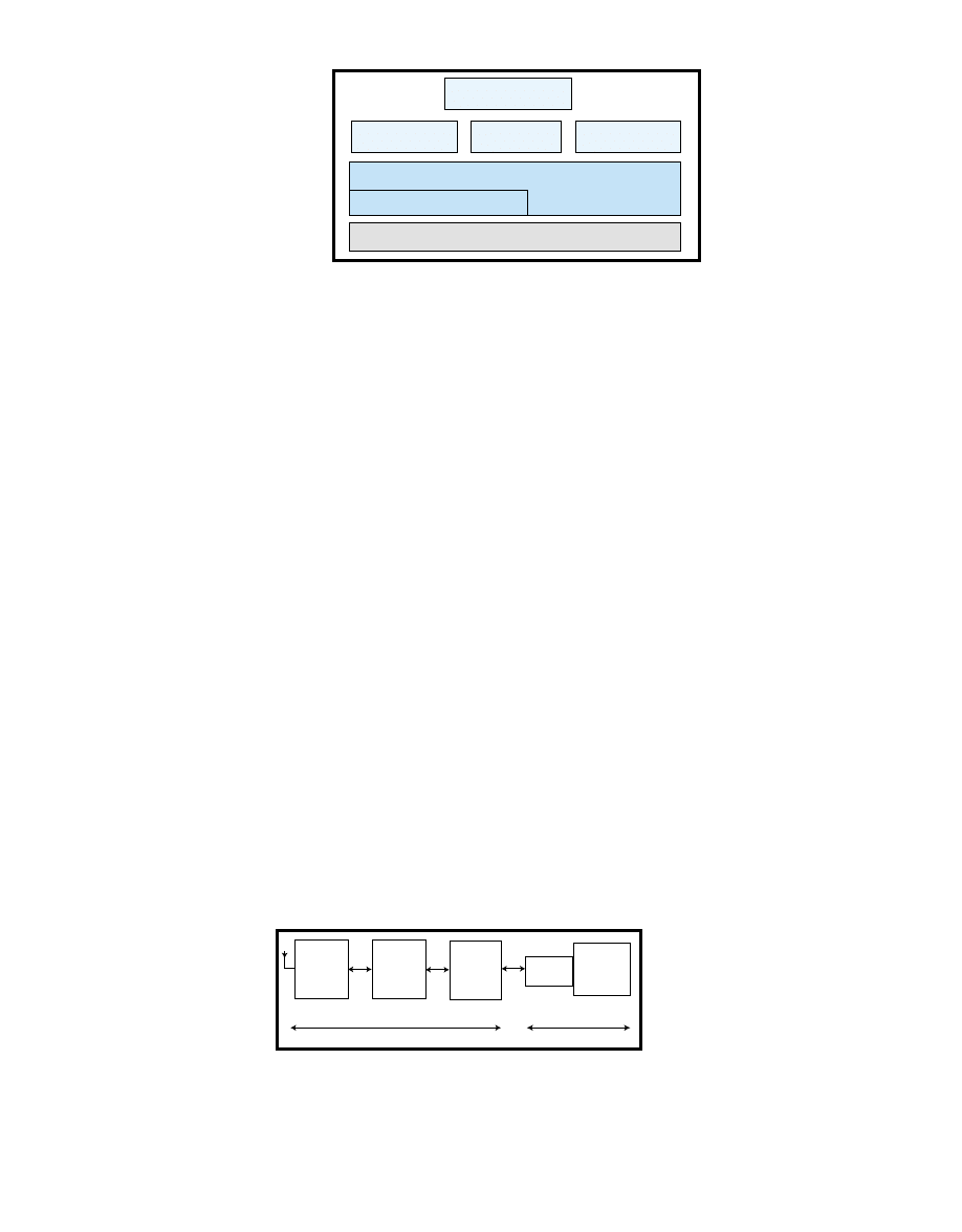
www.circuitcellar.com
CIRCUIT CELLAR
®
Issue 154 May 2003
45
conveys the quality of service informa-
tion. The telephony control protocol
defines the call control signaling for the
establishment of speech and data calls
between Bluetooth devices. RFCOMM
provides the emulation of serial ports
over the L2CAP protocol. The service
discovery protocol is used for locating
services provided by or available
through a Bluetooth device. Lastly, the
object-exchange protocol supports the
object-exchange usage model.
The protocol stack is implemented
to a different level in different profiles.
Several profiles have been defined for
typical usage scenarios: the cordless
telephony profile, intercom profile, seri-
al port profile, dial-up networking pro-
file, fax profile, LAN access profile, file
transfer profile, and synchronization
profile. There are certain requirements
that are common to all of these profiles.
The base profile is the generic
access profile, which defines generic
procedures related to the discovery of
Bluetooth devices and links manage-
ment aspects of connecting Bluetooth
devices. It also defines procedures
related to the use of different security
levels and includes common format
requirements for parameters accessi-
ble on the user-interface level.
Another base profile is the
service discovery application
profile, which defines the fea-
tures and procedures for an
application in a Bluetooth
device to discover services
registered in other Bluetooth
devices and retrieve any
desired available information
pertinent to these services.
GENERIC ACCESS PROFILE
The generic access profile
(GAP) introduces definitions,
UART): simply send and receive short
strings of data. You don’t need to worry
about complicated data buffering and
parsing, and there aren’t any commu-
nication state machines.
In this article, I’ll first introduce you
to Bluetooth. Then, I’ll describe the
software architecture, API, and various
usage scenarios.
A short time after publishing Blue-
port, the second generation of Bluetooth
modules appeared with a higher layer of
protocols—such us L2CAP and SDP—
embedded in the module. This created
the possibility to run user code inside
the module on top of the Bluetooth
stack. Such modules make the Blue-
tooth protocol stack used in Blueport
obsolete, because you can write code
concerning Bluetooth communication
inside the Bluetooth module using a
prequalified Bluetooth stack. This is
an important issue, especially when it
comes to the certification of a com-
mercial Bluetooth product.
Regarding these new modules, the
SPI-to-Bluetooth command parser is
implemented inside the module. Thus,
I’ll focus on simplifying Bluetooth
communication for applications run-
ning on small micros.
USING BLUETOOTH
The Bluetooth system offers both
point-to-point and point-to-multipoint
connections. In the former, several
Bluetooth units are connected to a
master unit and form a piconet (see
Figure 1a). The master controls all
communication. There is one master
unit and up to seven active slave units
in a piconet. Multiple piconets with
overlapping coverage areas are con-
nected together to form a scatternet
(see Figure 1b).
A typical configuration for
a Bluetooth network consists
of one master device with
several slave units around it.
For instance, a computer can
act as the master with a key-
board, mouse, printer, scan-
ner, PDA, and the slaves. In
addition, you could have a
DAQ device and several
measurement points in the
same area where each sensor
has a Bluetooth interface.
Other configurations aren’t as straight-
forward. You could have a master
device with slaves that have their own
slaves forming a large network of wire-
less interconnected devices. The most
important part of such a network is its
configuration—the way data is routed
from one network node to another.
BLUETOOTH PROFILES
A Bluetooth profile defines a selec-
tion of messages and procedures from
the Bluetooth SIG specifications; it
gives an unambiguous description of
the air interface for specified services
and cases. This ensures that Bluetooth
devices from different vendors can
interoperate without problems.
As you can see in Figure 2, the Blue-
tooth protocol stack consists of several
protocols laying on top of each other.
The baseband consists of low-level
link routines. For link set up and
control, the link manager protocol is
implemented. The signals are inter-
preted and filtered by the link manager
on the receiving side, and they aren’t
propagated to higher layers.
The logical link control and adapta-
tion protocol supports higher-level
protocol multiplexing, packet segmen-
tation, and reassembly. In addition, it
2.4-GHz
Bluetooth
radio
Bluetooth
link
controller
Bluetooth
link
manager
and I/O
Bluetooth
stack
Host
application
HCI
A
B
Figure 3—
Parts A and B are two distinct hardware modules in this typical
Bluetooth interface. Part A is the Bluetooth module, which consists of a radio part
and an ARM CPU running the low-level baseband, link controller, and firmware.
Part B is the application-specific module, which runs the Bluetooth user application
and higher layers of the protocol stack. Future Bluetooth modules will incorporate
the full Bluetooth protocol stack, and the host application will use an API to control
the stack in a similar way as done with Blueport (e.g., with AT commands).
Object exchange
protocol (OBEX)
Telephone control
protocol (TCS)
RFCOMM
Service discovery
protocol (SDP)
Logic link control and adaptation protocol (L2CAP)
Link manager protocol (LMP)
Baseband (link controller)
Figure 2—
Usually, the link
controller (LC) and LMP lay-
ers are implemented in the
Bluetooth module while the
rest of the protocol layers run
in an external microcontroller.
Communication between
these two components occurs
through the HCI. Blueport
frees resources in the host
microcontroller by running the
protocol stack in a separate
controller.
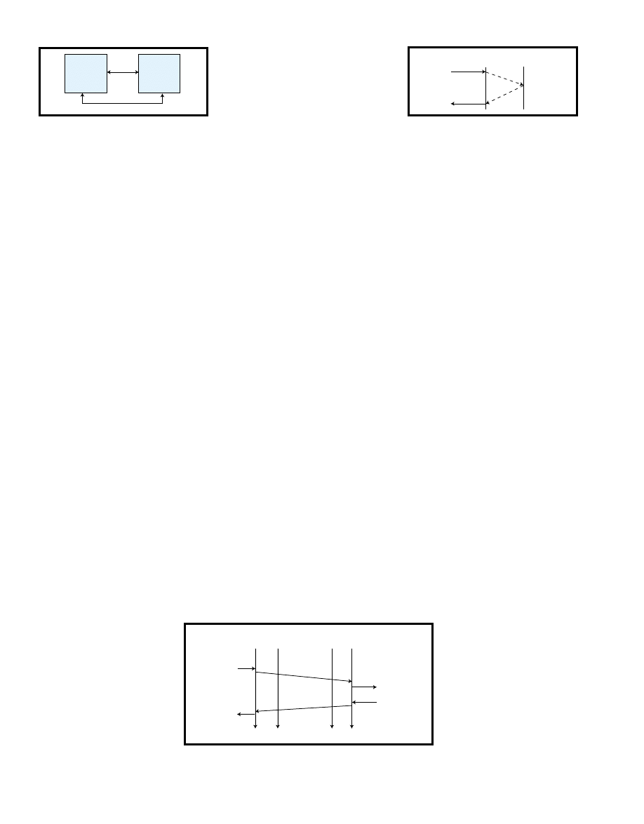
46
Issue 154 May 2003
CIRCUIT CELLAR
®
www.circuitcellar.com
recommendations, and common
requirements related to modes and
access procedures. These procedures are
used by transport and application pro-
files to describe how devices should
behave in standby and connecting
states. The purpose is to guarantee that
links and channels can be established
between Bluetooth devices and ensure
that multiprofile operation is possible.
The GAP handles the procedures
between two devices that are related
to discovery and connecting (establish-
ing a link and connection), particular-
ly in cases where neither device has
an established link. It’s also used
when one device has established a link
(possibly to a third device) before start-
ing the procedure.
In principle, you should be able to
connect any Bluetooth device to
another. Even if the two connected
devices don’t share a common applica-
tion, you should be able to find this
out using basic Bluetooth capabilities.
Bluetooth devices that don’t conform
to any other Bluetooth profile shall con-
form to this profile to ensure basic
interoperability and coexistence. The
most general configuration for a
Bluetooth device is supporting: General
Discoverable mode, to respond
to a device that makes a gener-
al inquiry; Connectable mode,
which responds to paging initi-
ated by other Bluetooth
devices; Security mode
(Security mode 1—it shall
never initiate any security pro-
cedure); the general inquiry
procedure, which provides the
initiator with the Bluetooth
device address, clock, class of
device, and used-page scan
mode of general discoverable
devices; the link establishment proce-
dure, which is used to establish a
physical link (ACL-type) between two
Bluetooth devices (HCI level of the
Bluetooth protocol stack); and the chan-
nel establishment procedure, which is
used to establish a Bluetooth channel
(i.e., a logical link) between two
Bluetooth devices (L2CAP level of the
Bluetooth protocol stack). As you can
see from the requirements, according to
the GAP, only partial implementation
of the HCI and L2CAP layers from the
Bluetooth protocol stack are mandatory.
BLUETOOTH HARDWARE
Bluetooth interface hardware is typi-
cally made up of the following: a Blue-
tooth chipset containing the radio front-
end; the Bluetooth controller (i.e., host
controller with an ARM core for the
baseband) in one or more chips depend-
ing on the chip vendor; and an embed-
ded processor (i.e., host from 8-bit to
powerful 32-bit processors) running the
Bluetooth protocol stack (and the appli-
cation). Figure 3 shows the typical con-
figuration for a system using Bluetooth.
There are several Bluetooth chip man-
ufacturers. Complete Bluetooth mod-
ules are also available where the hard-
ware necessary for running a chipset is
already put together. All of these mod-
ules have one thing in common: they
incorporate the radio and baseband con-
troller, offering the so-called HCI for the
embedded application to control the
module. The HCI can run on a UART
or through USB if higher communica-
tion speeds are needed.
HCI TRANSPORT LAYER
The HCI RS-232 transport layer
makes it possible to use the Bluetooth
HCI over an RS-232 interface between
the Bluetooth host and host controller
(see Figure 4). This is the lowest trans-
port layer of the Bluetooth stack; it’s
also the most suitable for small micro-
controllers because of the small code
size that’s necessary for a UART driver.
Communication in the Bluetooth
system is based on data packets with
predefined structures. Of the several
kinds of HCI packets that can be sent
via the RS-232 transport layer, the
most important are the following: the
HCI command packet, the HCI event
packet, the HCI ACL data packet, and
the HCI SCO data packet. Therefore,
if the HCI packets are sent via a com-
mon physical interface, an HCI packet
indicator must be added (see Table 1).
This is the first byte of the transmit-
ted packet. The HCI provides a uni-
form command method for accessing
the Bluetooth hardware’s capabilities.
HCI commands may take different
amounts of time to be completed; there-
fore, the results of the commands are
reported back to the host in the form
of an event. Thus, for most HCI com-
mands, the host controller will generate
the Command Complete event when a
command is completed. This event con-
tains the return parameters for the
completed HCI command.
The execution of an HCI
command results in a
Command Complete or
Command Status event fol-
lowed by the appropriate HCI
event generated by the com-
mand (e.g., the HCI create
connection command results
in a Command Status event
followed by an HCI Connec-
tion Complete event).
Figure 5 shows the general
communication diagram for
Bluetooth
host
Bluetooth
host
controller
HCI RS-232 transport layer
Bluetooth
HCI
Figure 4—
The Bluetooth module CPU—which runs
the low-level baseband, link controller, and firmware—
serves as the host. The host controller is the CPU that
runs the higher layers of the protocol stack. The host
and host controller can be connected via an RS-232
serial or USB (the so-called HCI transport layer), and
they exchange data in the form of HCI packets (com-
mand, data, and event).
Host
RS-232
Figure 5—
The host microcontroller sends HCI com-
mands to the host controller (running the baseband) to
create and destroy connections, and send data pack-
ets. As connections are created and destroyed, data
packets are received, and the host controller notifies
the host via HCI events.
L2CA_Request
L2CA_Confirm
Time
L2CAP_Response
L2CAP_Request
Initiator
L2CA
LP
LP
Acceptor
L2CA
L2CA_Indication
L2CA_Response
Figure 6—
Any operation request on the initiator side appears as an indication
on the acceptor side. A response on the acceptor side generates a confirmation
on the initiator side.
www.circuitcellar.com
CIRCUIT CELLAR
®
Issue 154 May 2003
47
the HCI layer. Flow control on the
HCI layer is achieved in different ways
for HCI commands and data packets.
For the former, the Command Status
and Command Complete events con-
tain the NumHCICommandPackets
event parameter, which allows the
host controller to indicate the number
of HCI command packets that the
host can send to the host controller. If
the host controller requires the host
to stop sending commands, the
NumHCICommandPackets event
parameter will be set to zero.
To indicate to the host that the host
controller is ready to receive HCI com-
mand packets, the host controller gen-
erates a Command Complete event
with the Command_Opcode 0x0000,
and the NumHCICommandPackets
event parameter is set to one or more.
Command_Opcode 0x0000 is an NOP
used to change the number of out-
standing HCI command packets that
the host can send before waiting.
For HCI data packets, flow control
is used from the host to the host
controller to avoid filling up the
host controller’s data buffers. During
initialization, the host sends the
Read_Buffer_Size command.
Two of the command’s return parame-
ters determine the maximum size of
HCI ACL and SCO data packets (exclud-
ing header) sent from the host to the
host controller. Two additional return
parameters specify the total number of
HCI ACL and SCO data packets that
the host controller can have waiting for
transmission in its buffers. It will also
send the Host_Buffer_Size command
to notify the host controller about the
maximum size of HCI ACL and SCO
data packets sent from the host con-
troller to the host. In addition, the com-
mand contains two command parame-
ters to notify the host controller about
the total number of ACL and SCO data
packets that can be stored in the data
buffers of the host.
The host controller uses the
NumberOfCompletedPackets event to
control the flow of data from the host.
This event contains a list of connection
handles and a corresponding number of
HCI data packets that have been com-
pleted (i.e., transmitted, flushed, or
looped back to the host). After it has
and applications to transmit and
receive L2CAP data packets up to
64 KB in length. On one side of the
communication channel, large L2CAP
data packets are split into several
smaller HCI data packets, transmitted,
and then reassembled into the original
L2CAP packet on the receiver side.
Because a Bluetooth device can be con-
nected to several different devices (dif-
ferent higher-level protocols), L2CAP
offers a unique layer understood by
every Bluetooth device to transfer data.
sent an HCI data packet, the host
must assume that the free buffer space
for the corresponding link type (ACL
or SCO) in the host controller has
decreased by one HCI data packet.
L2CAP LAYER
L2CAP provides connection-oriented
and connectionless data services for
upper-layer protocols with protocol-
multiplexing capability, data segmenta-
tion, and reassembly operations.
L2CAP permits higher-level protocols
CadSoft Computer, Inc., 801 S. Federal Highway, Delray Beach, FL 33483
Hotline (561) 274-8355, Fax (561) 274-8218, E-Mail : info@cadsoftusa.com
Schematic Capture • Board Layout
Pay the difference for Upgrades
You can use EAGLE Light for testing and
SMD pads can be rounded or round
Different pad shapes for Top, Bottom,
or Inner layers
48
Issue 154 May 2003
CIRCUIT CELLAR
®
www.circuitcellar.com
L2CAP is based on the concept
of channels. If two Bluetooth
devices want to exchange data,
they first establish a baseband
connection that will enable the
transmission of HCI ACL data
packets. Then, the two Bluetooth
entities will negotiate to estab-
lish one or more logical commu-
nication channels over the base-
band connection. (In this
instance, “logical” means that
there is a common physical con-
nection carrying several L2CAP chan-
nels.) A channel identifier refers to each
of an L2CAP channel’s endpoints.
Channel identifiers (CIDs) are unique
local names representing a logical chan-
nel endpoint on the device.
Figure 6 depicts communication over
the L2CAP layer. In order to make the
L2CAP layer interoperable between
Bluetooth devices, a well-defined state
machine must be respected. The state
machine is based on several opera-
tional states. In the Closed state, there
is no channel associated with the CID.
This is the only state in which a link-
level connection (baseband) may not
exist. Link disconnection forces all of
the other states into the Closed state.
In the W4_L2CAP_CONNECT_RSP
state, the CID represents a local end-
point. An L2CAP_ConnectReq mes-
sage is sent referencing this endpoint,
and it waits for the corresponding
L2CAP_ConnectRsp message. In the
W4_L2CA_CONNECT_RSP state,
the remote endpoint exists, and an
L2CAP_ConnectReq is received by the
local L2CAP entity.
The Configuration state is somewhat
different. In this state, the connection
is established but both sides still
negotiate the channel parame-
ters. The Configuration state
may be entered when the chan-
nel parameters are being renego-
tiated. Prior to entering, all out-
going data traffic should be sus-
pended, because the data traf-
fic’s parameters are to be renego-
tiated. Incoming data traffic
must be accepted until the
remote channel endpoint has
entered the Configuration state.
In the Configuration state, both sides
must issue L2CAP_ConfigReq mes-
sages. If only defaults are being used, a
null message should be sent. If a large
number of parameters need to be nego-
tiated, multiple messages may be sent
to avoid any MTU limitations and
negotiate the parameters incrementally.
Moving from the Configuration state
to the Open state requires both sides
to be ready. An L2CAP entity is ready
after it receives a positive response to
its final configuration request and has
positively responded to the final config-
uration request from the remote device.
Connection initiated
by host application
Connection initiated
by remote device
API
API
API
Blueport
SPI
SPI
Figure 7—
An action initiated by the host application (via an API call) gener-
ates an API event when Blueport finishes the requested operation. An action
generated by remote Bluetooth devices generates API events after Blueport
finishes processing. API calls and events are issued via an SPI interface.

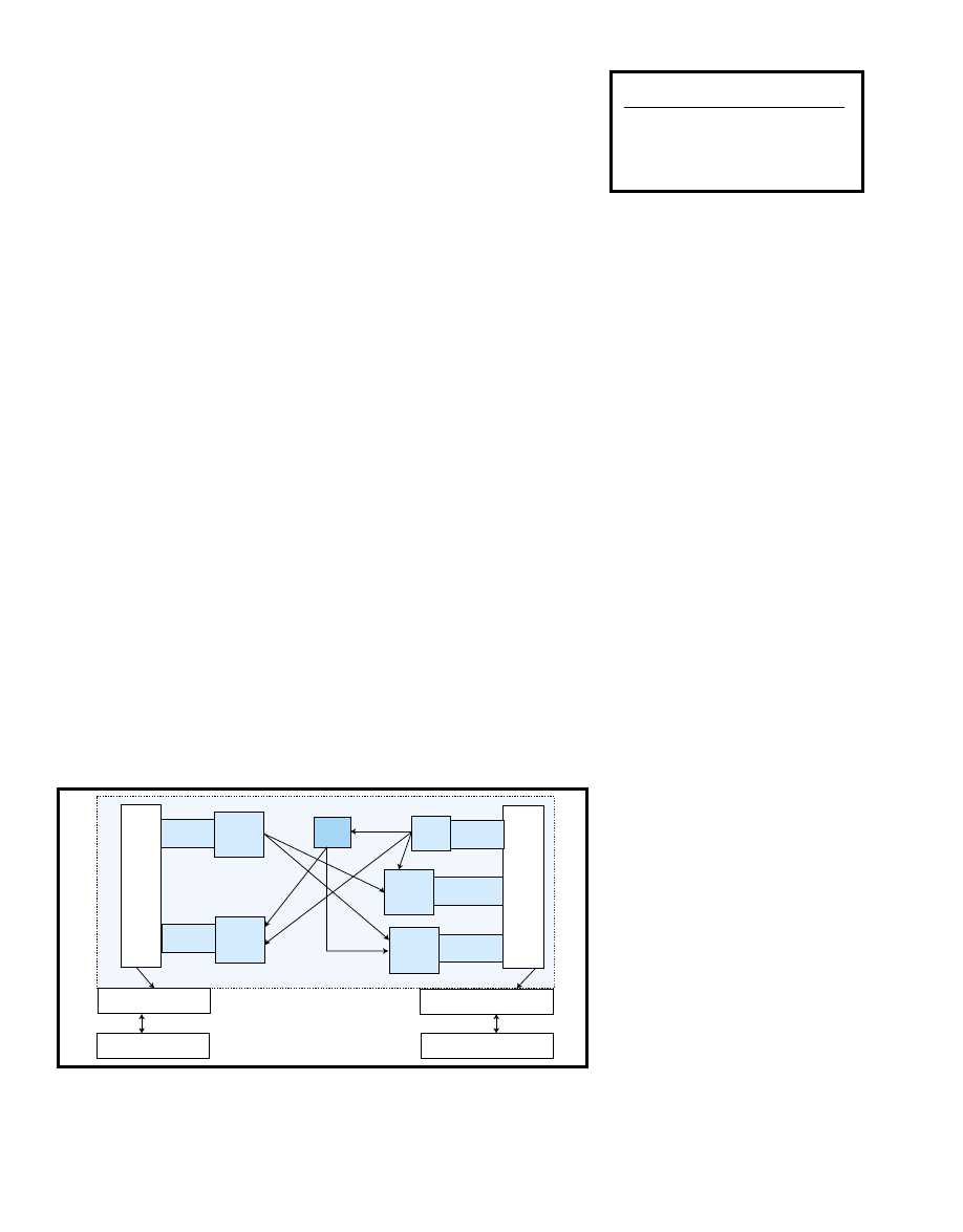
www.circuitcellar.com
CIRCUIT CELLAR
®
Issue 154 May 2003
51
In the Open state, the connection has
been established and configured, and
data flow may proceed. After channels
are established, logical channels
switch in this state.
The connection shuts down in the
W4_L2CAP_DISCONNECT_RSP:
state, and an L2CAP_DisconnectReq
message is sent. The state waits for
the corresponding response. In the
W4_L2CA_DISCONNECT_RSP: state,
the connection on the remote endpoint
shuts down and an L2CAP_Disconnect
Req message is received.
BLUEPORT COMMUNICATION
Blueport communicates with the
host microcontroller (application)
through an API accessible via the SPI
port. The general communication pro-
cedure involves sending API calls and
receiving API events. API events are
also generated when a remote device
initiates a connection. Only L2CAP-
level events are reflected in the API.
Figure 7 is a generic communication
diagram for the two possible situations.
The API calls have the following
generic format: length followed by
data, where length is the total length
in bytes of the API call represented as
a 16-bit unsigned integer sent in little-
endian format (i.e., LSB to MSB). All of
the variables represented on additional
bytes are sent in little Endian format.
The API events have the same
generic format as API calls. You may
download an example of the API from
the Circuit Cellar ftp site. Note that
the bytes prefixed by a “$” sign are
hex values. All of the other data are
ASCII characters, unless specified.
These APIs are accessible through
an SPI port. (AVR and Motorola
micros use a hardware port. For other
micros, it’s easy to make a software-
simulated SPI port.) Asynchronous,
bidirectional communication is need-
ed because events can be generated on
both sides of the SPI bus.
The SPI interface has several limita-
tions: the SPI interface is a synchro-
nous data bus where the SPI bus mas-
ter initiates data transfers; data trans-
fers can’t be initiated by the bus slave;
and data transfer from the slave to the
master is only possible when the mas-
ter is writing into the slave.
However, with an interesting solu-
tion, I’ve realized high-speed, asyn-
chronous, half-duplex, interrupt-driv-
en communication with the hardware
SPI between two AVR microcon-
trollers. Briefly, to send data from the
SPI slave to the SPI master, a master-
slave switch is performed whenever
one of the SPI devices would like to
transmit data to the other. It’s a half-
duplex communication.
SOFTWARE ARCHITECTURE
The software running Blueport must
handle tasks such as receiving HCI
packets (events and ACL data packets),
processing HCI packets, and handling
HCI events and L2CAP events/data.
Also, it must send HCI command/
response packets (events and ACL
data packets), receive API commands
through the SPI interface, and process
API commands. Finally, the software
must generate HCI/L2CAP commands
and API events.
Figure 8 represents the interoperabili-
ty of the different software modules.
The software must handle asynchro-
nous events coming from two sources,
the SPI and UART (both at high speed).
To overcome data loss and unreliable
operation, and to provide an efficient
memory usage, incoming data is stored
in large circular FIFOs. Outgoing data is
stored in large polygonal FIFOs.
A polygonal FIFO is an fixed-length
circular FIFO, where data (prefixed
with the length of the added data) is
stored. This technique is useful when
storing blocks of data of known length,
enabling block recovery of the space
used by the data chunks. In polygonal
FIFOs, data is always written and read
in blocks. When you don’t have an
operating system managing the mem-
ory, this is the fastest method and
requires the least amount of code.
The API commands are received in
the SPI input FIFO and processed by
the Blueport API parser, which
extracts API messages. Depending on
the nature of the API command, HCI
and L2CAP messages are generated
and stored in the HCI command out-
put FIFO and HCI data output FIFO.
Data from the Bluetooth module is
received in the HCI input FIFO and
processed by the HCI parser. If the
received data is an L2CAP packet, the
L2CAP parser processes it. The HCI
parser extracts HCI command/data
SPI
driver
SPI
input FIFO
Blueport
API parser
SPI
output FIFO
Generate
Blueport
API events
UART
driver
HCI
input FIFO
HCI
HCI commands
output FIFO
Generate
HCI
commands
HCI data
output FIFO
Generate
L2CAP
packets
L2CA
parser
To host application
HCI UART transport packets
API calls/events
To any Bluetooth
module supporting HCI
Figure 8—
The host application calls are processed by the Blueport API parser, which generates all of the neces-
sary L2CAP and HCI messages for the Bluetooth protocol stack. HCI and L2CAP packets generated by the
Bluetooth module (stack) as a result of a remote device action are processed by the HCI and L2CAP parser. After
completing a task, which may require several Bluetooth protocol stack actions, Blueport generates an SPI event.
The SPI driver handles SPI actions and events. The UART driver handles the HCI packets. Because of the highly
asynchronous operation and different handshaking mechanisms, data is buffered in from several FIFOs.
Table 1—
The second byte of an HCI packet is the
“HCI packet indicator,” which describes the type of data
carried by the packet. This indicator tells the protocol
stack how to handle the data received from the HCI
packet. The lowest layer of the Bluetooth protocol stack
parses the HCI packets.
HCI packet type
HCI packet indicator
HCI command packet 0x01
HCI ACL data packet 0x02
HCI SCO data packet 0x03
HCI event packet
0x04
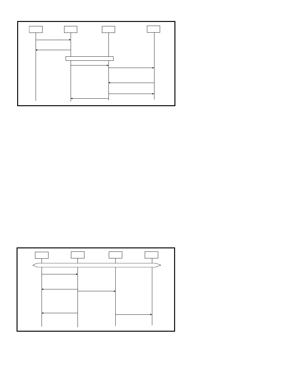
52
Issue 154 May 2003
CIRCUIT CELLAR
®
www.circuitcellar.com
packets. It also reassembles the
L2CAP packets segmented in multiple
HCI data packets.
HCI commands are generated when
it’s necessary to do so, and they’re
stored in the HCI command output
FIFO. The L2CAP parser generates
L2CAP command signals, HCI com-
mands, and Blueport API events. The
existence of different output FIFOs for
HCI commands and data is required by
the different flow-control mechanisms.
USING BLUEPORT
When communicating through a
device like Blueport, two scenarios are
possible. In the first instance, connec-
tion/data transmission is initiated to a
remote device by the Blueport host
controller. In the second, connection/
data transmission is initiated by a
remote device to the Blueport host
controller. Let’s begin with the former.
When an application uses Blueport to
connect to a remote Bluetooth device,
it has to perform certain steps. First,
sending the Blueport Initialize API ini-
tializes the Blueport module. After
returning successfully, the application
can send the Start Inquiry API. By exe-
cuting this API, the application
receives a list of BDADDR with all the
Bluetooth devices within radio range
that are in general discoverable mode.
With this list, the application can initi-
ate a connection to one of the remote
Bluetooth devices by calling the Create
Connection API. This API is handled in
void API_L2CA_Connect(u08* params).
Blueport checks if there are resources
for a new logical channel. If they exist,
it looks for a baseband connection to
the requested BDADDR. If there is a
connection, it uses it to establish the
new logical connection, starting the
L2CAP state machine for the new
channel by sending the Create
Connection L2CAP signal.
In the absence of a baseband connec-
tion to the requested BDADDR, Blue-
port sends the HCI Create Connection
command. The result is a Connection
Complete HCI event returning the con-
nection handle for the established base-
band connection. The successful cre-
ation of the baseband link will trigger
the L2CAP state machine.
The L2CAP state machine allocates
a new, unique local channel identifier
and sends the Connection Request
L2CAP signal. The result is a response
L2CAP signal—Connection Response—
returning the remote endpoint CID for
the logical channel and calling void
L2CA_ConnectInd (u16 PSM, u08*
rBDADDR, u16 lCID, u08 status). At
that point, channel configuration
begins between the two applications
running on the remote devices. After
negotiating the channel parameters, the
two applications start sending data to
each other. After receiving a complete
L2CAP data packet, the L2CAP parser
sends it to the application layer.
Data from the application to the
remote Bluetooth device is sent via the
Write Data API command and handled
by void API_L2CA_Write(u08* params).
Then, data segmentation is performed,
and the resulting HCI ACL packets
are sent to the remote via the base-
band connection. After sending the
data, a Data Write confirmation event
is generated to the application by call-
ing void L2CA_WriteInd(u16 dCID,
u16 lgth, u08 status).
The data received by Blueport from
remote devices is assembled in
L2CAP packets by the HCI parser.
Then, it’s sent to the host application
generating a Data Received event call-
ing: void L2CA_ReceiveInd (u16
dCID,u16 lgth,u08* pdata).
After the data is transferred, the
application can close the logic channel
to a remote BDADDR by sending the
Disconnect Channel API call handled
by void API_L2CA_Disconnect(u08*
params). Blueport initiates the logical
channel closing sequence of the
Host A
HC/LM-A
HC/LM-B
Host B
Page and page response
/*Master-Role*/
HCI Create_Connection
(BD_Addr, Packet_Type,...)
LMP_host_connection_reg 0
LMP_accepted (opcode)
HCI Connection request event
(BD_ADDR, CoD, Link_Type = ACL)
HCL_Accept_Connection_Request
(BD_ADDR, Role = Slave)
HCI Command status event
(Status, Num_Cmd,Cmd_OpCode)
/*Slave-Role*/
HCI Command status event
(Status, Num_Cmd,
Cmd_OpCode)
Figure 9—
Host A initiates the creation of the connection, and Host B accepts or rejects the connection request. All of the
processing is done in Blueport. The host application is free to do whatever is necessary until the connection is created.
Host A
HC/LM-A
HC/LM-B
Host B
HCI _Disconnection
(ConHandle, Reason)
LMP_detach (reason)
HCI Disconnection
complete event
(Status=0×00,
ConHandle, Reason)
HCI Command status event
(Status, Num_Cmd,
Cmd_OpCode)
HCI Disconnection
complete event
(Status=0×00,
ConHandle, Reason)
/*ARQ-Ack*/
ACL connection established
Figure 10—
Here you see the detailed HCI and baseband data flow to disconnect two Bluetooth devices. Host A initi-
ates the disconnection. Both Host A and Host B will be notified when the baseband is disconnected. All of this processing
is done in Blueport. The host application is free to do whatever is necessary until the connection is
destroyed.
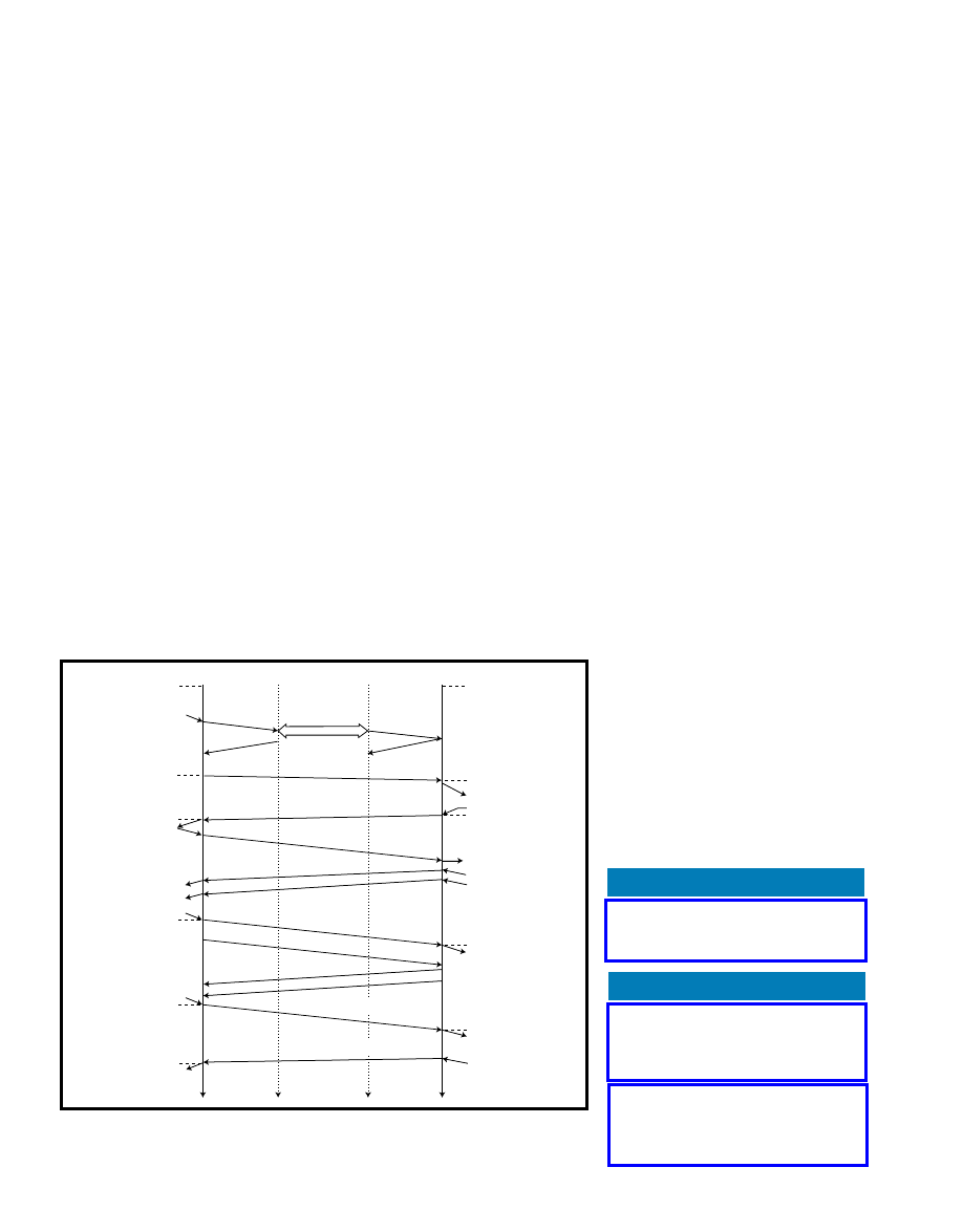
www.circuitcellar.com
CIRCUIT CELLAR
®
Issue 154 May 2003
53
Zoltan Molnar holds a Master’s degree
in Electromagnetic Compatibility from
The Technical University of Cluj-
Napoca, Romania. Currently, he’s an
independent contractor working for
companies in need of project evalua-
tion, hardware/software development,
and prototyping. His technical inter-
ests include industrial automation and
artificial intelligence. Zoltan’s web site
address is microhardsoft.itgo.com.
SOURCES
AT90S8515 Microcontroller
Atmel Corp.
(408) 441-0311
www.atmel.com
ROK100108 Bluetooth module
Ericsson, Inc.
(972) 583-0000
www.ericsson.com
PROJECT FILES
To download the code, go to
ftp.circuitcellar.com/pub/Circuit_
Cellar/2003/154/.
Author’s note: I’d like to thank
Microgigacomm for its support as I
worked on this project.
mission is initiated by a remote
device. Any Bluetooth device can con-
nect to Blueport. Note that Blueport
will receive HCI connection request
events when a remote device wants to
create a connection to the application
hosting it. If resources are available
(i.e., the maximum number of base-
band connections isn’t reached),
Blueport will accept the connection
request; otherwise, it will reject it.
Following the creation of a baseband,
the remote will initiate the L2CAP sig-
naling state machine sending L2CAP
signals. Blueport responds to these sig-
nals with the corresponding response
packets. If there are resources for a
new L2CAP connection, the logical
channel creation is accepted and a new
channel identifier is allocated.
When the channel is opened (accord-
ing to the Bluetooth specification is in
Configuration state) a Connection
Complete is generated to the application
with the logical channel identifier and
the remote device BDADDR embedded
in the API event. The next step involves
logical channel parameter negotiations.
After completing the logical channel
configuration, the two applications can
L2CAP state machine, sending the
Disconnect Request L2CAP signal,
which results in the Disconnect
Response L2CAP event. At that point,
the logical channel is closed, and fur-
ther data transfer is impossible. The
application is notified about the clos-
ing of the logical channel through the
Disconnection Complete API event
that’s generated by calling void
L2CA_DisconnectInd(u16 lCID).
Blueport checks for open logic chan-
nels on the baseband connection where
the last logical channel was disconnect-
ed. If there are no other logical channels,
the baseband connection is disconnected,
and Blueport sends the HCI Disconnect
command for the handle correspon-
ding to the connection to BDADDR.
Figure 9 shows the creation of a
baseband connection between two
remote Bluetooth devices using HCI
commands. The disconnection of a
baseband link between two remote
Bluetooth devices is depicted in
Figure 10. Finally, Figure 11 portrays
the communication between two
remote L2CAP entities.
Now, let’s take a look at what hap-
pens when a connection/data trans-
Initator
LP
LP
Target
[Closed]
[Closed]
L2CA_ConnectReq
LP_ConnectReq
L2CAP_ConnectReq
LP_ConnectCfm
LMP
LP_ConnectLnd
L2CA_ConnectInd
[W4_L2CA_ConnectRsp]
[W4_L2CA_ConnectRsp]
L2CAP_ConnectRsp
L2CA_ConnectRsp
L2CA-ConnectCfm
L2CA_ConfigReq
L2CAP_ConfigReq
L2CA_ConfigInd
[Config]
L2CA_ConfigRsp
L2CA_ConfigReq
L2CAP_ConfigRsp
[Config]
L2CA-ConfigCfm
L2CA-ConfigInd
L2CA-ConfigRsp
L2CAP_ConfigReq
L2CAP_ConfigRsp
L2CA_ConfigCfm
Data
[Open]
[Open]
Data
Data
L2CA_DisconnectReq
L2CAP_DisconnectReq
L2CA_DisonnectInd
[W4_L2CA_DisonnectRsp]
[W4_L2CA_DisonnectRsp]
L2CA_DisconnectCfm
[Closed]
L2CA_DisonnectRsp
[Closed]
LP_ConnectRsp
L2CAP_DisconnectRsp
Figure 11—
The initiator (target) Blueport issues (processes) all of these commands. The host application is free to
do whatever is necessary until these operations are completed. This is how Blueport makes Bluetooth connectivity
easy (even with small microcontrollers).
transfer data until one of the devices
sends a Disconnect request. After the
logical channel is closed, Blueport auto-
matically frees the allocated resources,
making possible the creation of a new
Bluetooth connection.
BENEFITS
Protocol adapters like Blueport are
useful for connecting simple embed-
ded systems to complicated technolo-
gies like Bluetooth. They keep things
simple for the original application and
encapsulate the functionality brought
by these new technologies.
Another benefit associated with
Blueport-like solutions—with a cus-
tom unqualified Bluetooth protocol
stack and first-generation Bluetooth
modules—is that they help you develop
proof-of-concept products. Thus, time
is saved for developers and customers
until Bluetooth technology becomes
mature and well supported by chips,
modules, and software.
I

54
Issue 154 May 2003
CIRCUIT CELLAR
®
www.circuitcellar.com
ast month, I
continued my dis-
cussion of the Home
Control System II (HCS)
FPGA upgrade by describing the FPGA
design. Now, in this final article, I’ll
show you how to incorporate the FPGA
with additional circuitry to provide the
complete upgrade solution. This will
include using the modified HCS II
firmware and new capabilities in the
XPRESS compiler 5.0 that take advan-
tage of the new FPGA upgrade functions.
HARDWARE REQUIREMENTS
First, you’ll need to obtain the hard-
ware (or reasonable equivalences) I used
for my upgrade (see Figure 1). There are
only a few parts you’ll need to add to the
FPGA upgrade—the toughest one to get
will be the FPGA itself. I used the Xilinx
XV2000E-1156 BDA, which is expensive,
but mine came on a board that was no
longer needed at my workplace.
You can use any part that’s big enough
(100,000-gate range). As I’ve mentioned
before, the Xilinx XCS2-100 is a good
candidate. Altera’s 10K100 and 20K100
as well as Xilinx’s XV300E should all
work, but be sure to synthesize, place,
and route the design before spending
any money. Make sure you can get the
design to fit. Try to scrounge the parts
from old boards, and obtain several parts
because there’s always the risk of acci-
dentally miswiring and damaging a part.
Make certain you have at least
91 pins free. That gives you 16 inputs
and 16 outputs, which is more than the
old HCS II. But, note that the 16 inputs
and eight outputs of the old board are
still available, as well—at least until
the board is upgraded to the Rabbit
3000. Even then, I plan to provide the
extra inputs and outputs. In any event,
a minimum of 91 I/O pins is required.
You also need an 18.432-MHz oscil-
lator, EPROMs for the FPGA configura-
tion (three XC18V04 flash memory
EPROMs, in my case), and a 1.8- and
3.3-V regulator (or whatever value you
need for your FPGA power and support
circuitry). A 70-ns 27C256 EPROM is
essential. Although it’s not shown on
the schematic, this is the EPROM that
goes on the original HCS II processor
board and holds the updated firmware.
Several bypassing capacitors, a 10-pin
JTAG Molex header, eight LEDs, one
eight-position DIP switch, and two 26-
pin connectors to the HCS II daughter
card stack are also required. Obtain a
female PS2 board mount connector for
a PC-compatible keyboard and various
connectors for the serial RS-232 ports
(e.g., the Scott Edwards G12864 LCD).
Finally, you will need up to four
ISD4003-8 voice chips, which are now
sold by WinBond. The custom board is
shown in Figure 2. Figure 3 depicts the
voice chip circuitry.
To learn more about the HCS II stack
connector signal placement shown in
Figure 2, you may refer to my web site
(www.zetaengineering.com), hcs.source
forge.com, or the HCS II manual docu-
mentation. Be sure to get the physical
location and orientation of where to
place these connectors. Don’t make the
mistake of placing them wrong side up
or side by side in the wrong fashion: it’s
extremely easy to get confused.
In my implementation, because I had
a separate board that contained the
FPGA, I added connectors to the cus-
tom board that were compatible with
those already present on the FPGA
board. I put sensor buffers and protec-
tion circuitry on the custom board.
Don’t even think about routing FPGA
outputs directly to sensors or drive out-
Updating the Home Control
System
l
Now that you’re famil-
iar with Robert’s
FPGA design method-
ology, it’s time to get
your hands dirty. In
the final installment of
his series, Robert
describes the hard-
ware, firmware, and
software you’ll need
to start working on a
home automation
project of your own.
Robert Morrison
FEATURE
ARTICLE
Part 3: The Complete Upgrade Solution
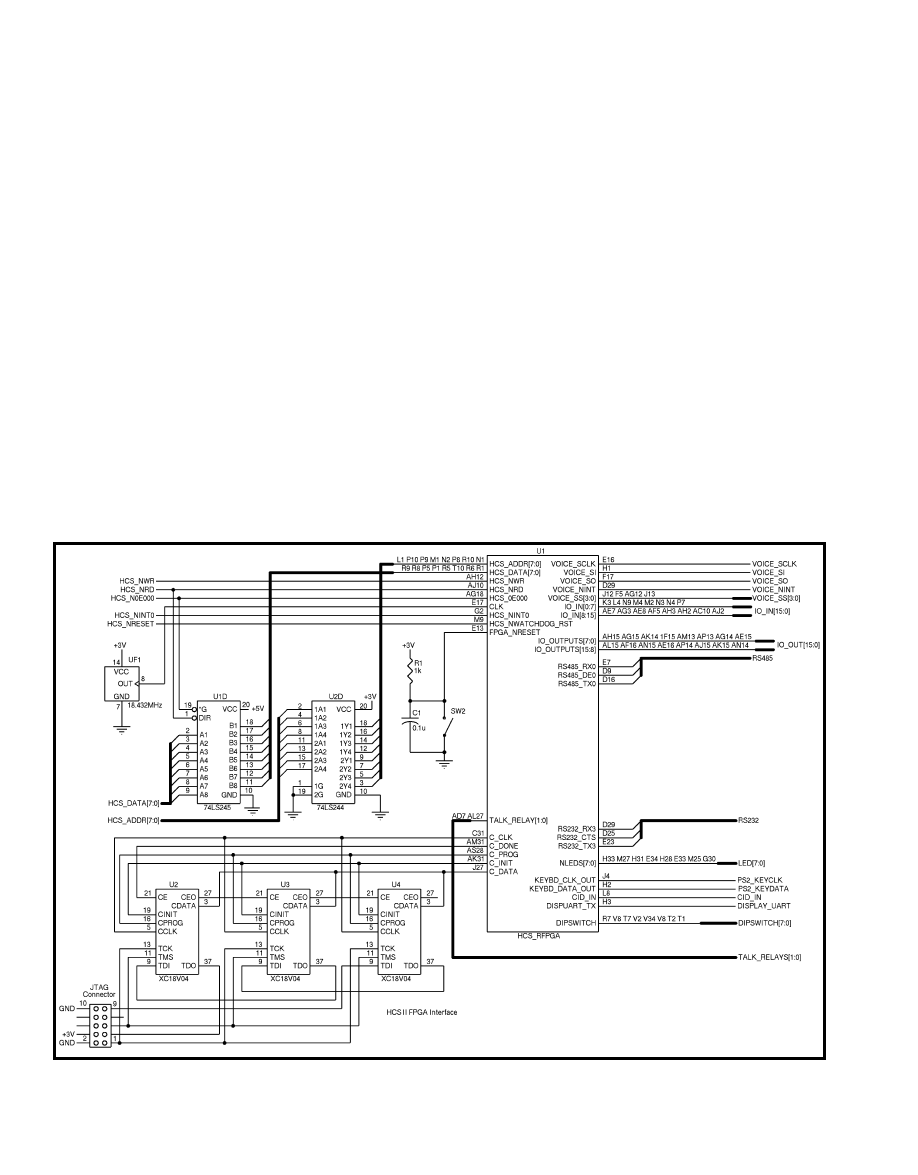
www.circuitcellar.com
CIRCUIT CELLAR
®
Issue 154 May 2003
55
the FPGA upgrade, and what do you
need for firmware and software? The
first decision to make is whether you
want to customize the FPGA or sim-
ply implement the version I used. Be
aware that this isn’t a commercial
effort with a friendly (or not so friend-
ly!) phone support line. You’ll have to
carry through on your own, although
many of us in the Circuit Cellar HCS
II newsgroup will help with reason-
able requests.
So, if you’re a beginner, your expecta-
tions should be based on your ability to
carry them out. If you are experienced
with FPGA design and synthesis, then
you’ll be in a position to make custom
modifications or use the source code
for a different FPGA than mine. If not,
just use my FPGA bits and wire it up
as I have done. After the HCS II com-
munity settles on a particular FPGA
that isn’t as expensive as mine, bits
will be made available, either on my
web site or the Source Forge site.
puts. You don’t want to ESD zap your
FPGA! Protect any signals that go out
of the system by buffering them. Use
optoisolators, relays, or other forms of
isolation for signals that go throughout
the house, because those lines can pick
up significant coupled voltages.
I also buffered the address and data
lines connected to the daughter card
interface. The timing of the faster main
board is tight, so don’t load down the
data bus any more than you have to.
The voice chip interface is straightfor-
ward: simply hook up the appropriate
pins from the FPGA to the SPI interface
of the voice chips, connect your comput-
er’s sound card line out to the voice
input via capacitors (it can be removed
after you store your voice messages), and
attach the voice output to your sound
amplifier. I recommend using relays to
route the amplifier sound outputs to the
desired source; otherwise, you’ll have to
deal with constant hissing and hum-
ming (e.g., from your intercom).
Lastly, I bought a small caller ID
module and took it apart. Inside, I found
a tiny UART signal chip. (Caller ID uses
a 1200-bps FSK. Don’t go through the
hassle of creating a safe phone interface
unless you know what you’re doing.)
You should try to find the TTL-level
output from this chip that provides the
FSK decoded UART-compatible output.
I buffered this signal and sent it to the
appropriate FPGA pin. I used an old
ATT caller ID module, which meant I
didn’t have to deal with the FSK
decoding and phone-line isolation.
Because the ring voltage goes up to
90 V, I don’t recommend reinventing
the wheel, although finding a CID
module that provides this output may
require a little gambling and luck. You
may have to buy a few of these until
you find one that has what you need.
They cost between $5 and $10 each.
CUSTOMIZE THE UPGRADE
So, how do you go about building
Figure 1—
Take a look at the components on the FPGA board attached to the custom board (i.e., stacked on top of the existing HCS II system). The configuration EPROM
data is loaded into the FPGA at power-up, at which time it activates the circuitry implied by the EPROM data. The JTAG connector shown in the lower left permits the in-circuit
programming of the EPROMs.
56
Issue 154 May 2003
CIRCUIT CELLAR
®
www.circuitcellar.com
OK, suppose you want to make cus-
tom changes to the FPGA. You can start
with the source code that I synthesized
and make modifications. Then, you’ll
need to get synthesis tools such as
Synplicity or Leonardo Spectrum. You
could also use the Xilinx ISE V.4.2i or
Altera Quartus II V.2.1. With these,
it’s easy to roll your own. Download
the Verilog source code, download the
pin-out file, make the modifications
(first make sure you can synthesize the
original and get it to work before adding
your changes), and synthesize for
20 MHz. Xilinx’s ISE WebPACK is a
great place to pick up the tools for
smaller devices; it’s available for free
on the company’s web site.
If you want to tweak the source code
for your own use, that’s great—but I rec-
ommend taking steps to maintain com-
patibility or your effort won’t be share-
able or easy to integrate into newer ver-
sions (e.g., keeping your changes in a
separate include file so you can easily
use upgraded base versions). I’m keeping
a registry of used FPGA registers. You
can get this information from my web
site or hcs.sourceforge.com. The loca-
tions 0xE0 through 0xFE are permanent-
ly reserved registers used specifically for
custom modifications. If you think other
designers will find your feature useful, I
will add those registers to the area that
isn’t customized and probably put the
module in the standard FPGA source.
One way or the other, you can get the
bits necessary to configure your FPGA.
There are several ways to go about set-
ting up the HCS II system to configure
your FPGA. I have FPGA configuration
EPROMs on my FPGA board. I think
this is the best way because it seems to
be the simplest. Most FPGAs these days
are not EPROM-based (i.e., have inter-
nal EPROM); they have internal-config-
uration SRAM memory that’s loaded at
power-up. This information can be sup-
plied using configuration EPROMs via
several FPGA pins, or you can use a
microprocessor or byte-wide EPROM
to load the FPGA from memory.
Because the FPGA is inactive during
loading, I don’t like either of the afore-
mentioned approaches because the
FPGA can’t be used for address decod-
ing or other processor-related functions
(it’s not awake until after the processor
is done loading it). In addition, the nec-
essary configuration code can take up a
significant chunk of available proces-
sor ROM space. By providing a JTAG-
programming interface for the FPGA
configuration EPROMs, it takes only a
few minutes to synthesize design revi-
sions to the FPGA and then load them
in the configuration EPROMs.
The JTAG interface is an industry-
standard way of communicating with
chips already mounted on a PC board;
it’s basically a specialized serial inter-
face for programming, verifying, or
troubleshooting chips. You need a spe-
cial JTAG connector on your FPGA
board connected to the corresponding
JTAG pins of the FPGA configuration
EPROMs. You also need a JTAG
adapter that plugs into the parallel
port of the PC. They are easy to make,
or you can buy them from suppliers
like Xilinx for approximately $100.
UPGRADE SOFTWARE
After wiring the FPGA upgrade, you


International Engineering
Consortium
www.iec.org
International Engineering
Consortium
www.iec.org
Network
and
Learn
with Design Engineers on the East Coast
D
esignCon East delivers technology solutions to engineers
and business decision-makers of the East Coast design-
engineering community. DesignCon’s proven program of
technical presentations, technology demonstrations, and candid
discussion with industry leaders offers practical solutions to
today’s design-engineering challenges.
Conference Chairperson
Edward Sayre
President and Chief
Executive Officer,
North East Systems
Associates, Inc.
Keynote Addresses
Bernard Gordon
Executive Chairman and
Chairman of the Board
Analogic Corporation
Cherry Murray
Senior Vice President,
Physical Sciences
Research Lab,
Bell Labs
Lucent Technologies
GianGuido Rizzotto
Director, Corporate
Technology Research
and Development
ST Microelectronics
Conference:
June 23–25, 2003
Exhibition:
June 24–25, 2003
Royal Plaza Hotel and Trade Center
Marlborough, Massachusetts
The Meeting Place for Design Engineers
24 sessions featuring the
following:
• High-Performance System Design
• System-on-Chip and ASIC Design
• Technology Exhibits
• IEC Executive Program
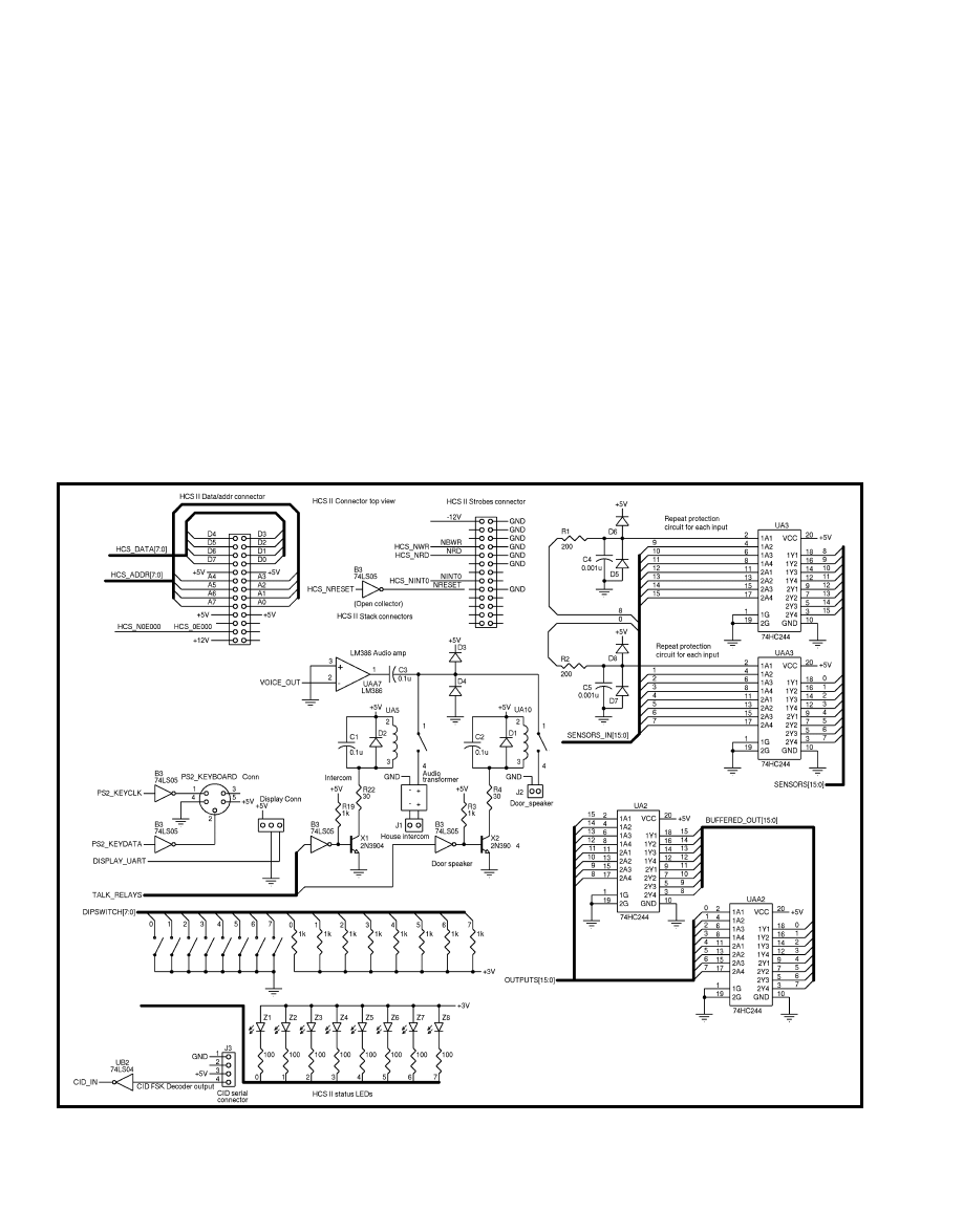
www.circuitcellar.com
CIRCUIT CELLAR
®
Issue 154 May 2003
59
can turn it on. But first, you need to
get the appropriate firmware and soft-
ware. Please remember that my version
is a spin-off version—it’s only a propos-
al. Other members of the HCS II com-
munity manage the official firmware
effort. They will choose what to
include in the HCS upgrade path.
The software for HCS-R consists of
three parts: the host.c program, the
ROM firmware code, and the XPRESS
compiler code. The firmware code is
the stuff that the processor runs on;
it’s the code that’s constantly checking
the house status and issuing data to
outputs or serial ports. It can also com-
municate with the console, which is
usually a PC hooked up to the RS-232
connector on it HCS II main board.
When you want to load a new home
control program into it, you aren’t
Does any of this make sense? Here’s
a summary: first, write a source code
file called events.hcs (you may down-
load a small sample from the Circuit
Cellar
ftp site); second, compile it with
hcs_comp.exe to generate an events.bin
file; third, run the hosts.exe file to
begin communicating with the system
(this assumes that the RS-232 connec-
tion is valid); and finally, type the let-
ters
F (file) and L (load) to download
the recently compiled events.bin file.
Of course, this assumes everything is
working. Make sure the hcs_comp.exe
and the firmware that’s programmed
into the firmware ROM are the same
version, or the events.bin file will not
be loaded. There are several things that
can go wrong if the hosts.exe file is
unable to communicate with the
HCS II program. Data rates and RS-232
actually reloading the firmware, you’re
just loading (from the PC) a series of
tokens that reflect the commands you
specify with the events.hcs source pro-
gram. You use the HCS II XPRESS
compiler hcs_comp.exe executable to
compile your events.hcs file into a file
containing tokens called events.bin.
Use the host’s executable (hosts.exe) to
talk to the module via the RS-232 con-
sole interface. This allows you to tell
the system to perform a variety of
commands via the PC, such as down-
loading your recently complied
events.bin file.
After downloading the new
events.bin file, the system restarts at
the beginning of your events program.
At that point, you can disconnect the
console connector, and the HCS II will
run by itself without your intervention.
Figure 2—
This schematic shows most of the glue logic present on the custom board and interconnects to the FPGA shown in Figure 1. Note the simple protection circuitry for
the sensor inputs. Be sure to use more capable protection for signals that are routed throughout your house. Relay drivers are provided to keep spurious noise off of the inter-
com and doorbell audio when they are not being used.
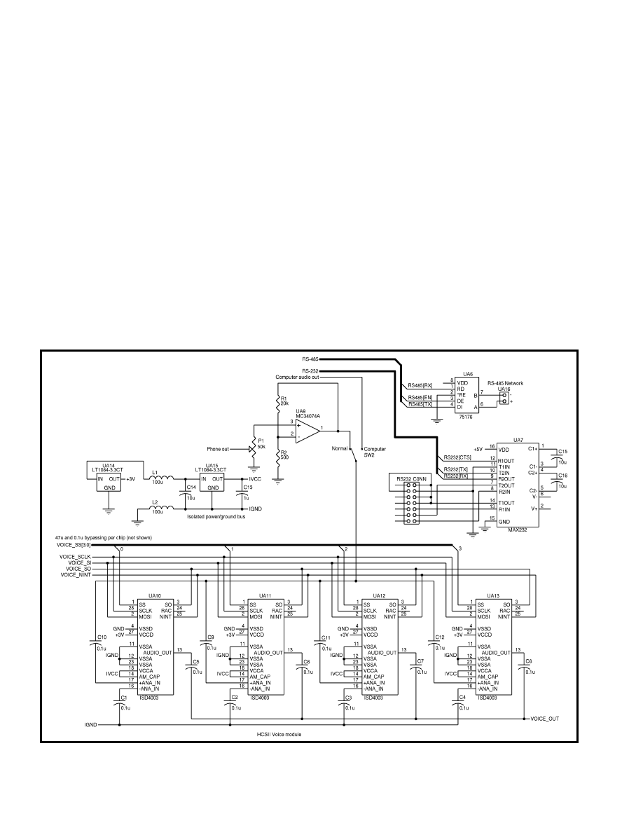
60
Issue 154 May 2003
CIRCUIT CELLAR
®
www.circuitcellar.com
options must be identical. You must
have the correct serial port connectors
(transmit and receive must not be
swapped), and so on—the usual pain of
trying to get two RS-232 devices (PC
and HCS II) talking. When it’s working
correctly, you’ll see the time updating
every second in the host’s window.
Now, what do you need to do to get
the latest FPGA upgrade working?
First, pick up the sources for the
hcs_rom and hcs_comp executables.
The hcs_rom.asm source file is a Z180-
compatible assembler file that uses two
included files (i.e., osmacro.asm and
ports.lib). I picked up a free assembler
from the Zilog web site (you must
register), and assembled the file into
an Intel hex-compatible binary.
Next, you have to program a 70-ns
27C256 EPROM. I’ll put bits on my web
site if you don’t want to try to assemble
the source code. (Note that the Source
Forge web site keeps compiled bits for
the EPROM, as well.) After you have
an EPROM, swap the existing EPROM
with the new one. Don’t reprogram the
existing HCS II EPROM. Use a new
EPROM. Otherwise, if something does-
n’t work, you won’t be able to go back
to something that worked. As usual,
use ESD precautions to prevent damag-
ing the EPROM or HCS II system.
The next step is to compile the
XPRESS compiler host_comp.c file.
Just about any C compiler for the PC
should work. I used the old Microsoft
32-bit C++ compiler. You need the
host.exe executable. I haven’t made
any changes to it. There aren’t any
modifications to the host program, but
the HCS ROM and XPRESS compiler
have been modified extensively. You
may pick up sources for these at my
web site in the HCS download section
or from hcs.sourceforge.com.
You can use a version of a C com-
piler for the XPRESS compiler, just be
sure to compile it as a DOS exe-
cutable. (Other developers have put
Windows application versions on the
Source Forge web site, but I haven’t
tried them yet.) I run on Windows
98SE. Because I dislike Microsoft’s
intrusive registration and cheesy mar-
keting on Windows XP, I haven’t
upgraded. I will probably go to Linux
for my next operating system (OS)
upgrade, but for now, I’ll stick with
Windows 98SE. This shouldn’t really
matter, though, because all of this
should be OS-independent.
If you find new bugs that aren’t on
the bug list (hcs_buglist), then send
me an e-mail. I’ll add it to the list,
and see if I can find the time to fix
it. Until then, you’re certainly free to
use the aforementioned procedures to
fix them yourself.
Figure 3—
When working on the voice chip interface, don’t forget individual caps on the analog circuitry—even though the analog inputs are inputs, they can’t be tied together
for multiple chips. The op-amp circuit allows for the recording of messages. The switch permits a computer or amplified microphone to supply default phone system messages
when desired (e.g., to perform the initial recording,
pf
the phone answer messages).

www.circuitcellar.com
CIRCUIT CELLAR
®
Issue 154 May 2003
61
There are numerous changes from
the version 4.01 XPRESS compiler to
my latest version (5.02 as of this writ-
ing). Because this version includes the
INBYTE, OUTBYTE, and OUTSTR func-
tions, which work on FPGA registers 0
through 0xFF, you can address the
FPGA registers as follows:
ifa inbyte(0) = 0x55 then
outbyte(8) = 45
You can use defines to make it easier
to reference your custom FPGA registers
such as 0xF0. I have an include file that
has all of the standard FPGA defines
for FPGA registers. If you want to mod-
ify the compiler or the ROM, the
source code for the latest version is
available on the Circuit Cellar ftp site
and hcs.sourceforge.com. Simply set up
a system so you can merge your cus-
tomized stuff into updates to the stan-
dard version. I resist doing this, because
I’m likely to go through quite a few revi-
sions of the source, but it’s up to you.
I have added much more FPGA reg-
ister support, as well as numerous
byte-oriented support commands to
XPRESS, such as the ability to specify
a bit within a byte,
AND, OR, NOT, and
logical
AND, OR, and NOT functions
(they are not the same!). In the future,
I may add procedure and case state-
ments, although discussions need to
take place and a consensus should be
reached among the HCS II communi-
ty before those steps are taken.
XPRESS 5.02
The XPRESS 5.02 compiler includes
several enhancements: FPGA support
via
INBYTE(xxx), which is input from
the FPGA register xxx;
OUTBYTE(xxx),
which is the outputs to FPGA register
xxx; and
OUTSTR, which output a
string to the LCD on the HCS, not
the networked LCD in the original
HCS II. The list of enhancements also
includes hex numerical syntax for
operands (e.g., 0x55) and new operators,
such as
&, |, and ~ (i.e., bitwise AND,
OR, and NOT functions for equations).
The new operators—
AND, OR, and
NOT—are logical operators for equa-
tions. These operators already exist
for
IF expression clauses. This new
capability expands this to equations.
For instance,
variable(3) = (keybd
= 0x31) OR (keybd = 0x32).
There is a new operator,
BIT (e.g.,
“A BIT b” selects the b bit of A). The
new escape character for strings,
%Fxxx, displays the hexadecimal con-
tents of the xxx FPGA register.
As a new escape character for strings,
%Xn displays a listed variable or port in
hexadecimal form with n digits (up to
four). The
keybd operand displays the
last character typed into the keyboard.
An additional enhancement is full
support for the FPGA automatic
interrupt-vectoring system. At power-
up, the HCS II firmware loads the
FPGA interrupt vector SRAM with
vectors to all available FPGA inter-
rupts. Interrupt routines are provided
for all FPGA functions, and they exe-
cute automatically in the background.
The
Cid command allows for the
reading of a current phone caller’s
index number. The
phone (n) com-
mand allows setting the
n registry
entry with a 10-digit phone number
that’s automatically matched with
the current incoming caller ID.
It’s extremely easy to modify the
firmware and compiler source code to
do what you need. (Please be sure to
keep the relevant copyright notices in
the files you modify.) Note that because
there is no single source for the HCS II
code, people will have different ideas.
Therefore, I’ve tried to be careful to not
cause a split or dissension among users.
This is a spin-off effort that may or
may not get folded back into the
official HCS II path. These features
are meant to be enhancements with
generic appeal, but they were present-
ed without significant discussion with-
in the HCS II community.
MORE TO COME
The HCS II is a great home system;
it provides effective coverage for most
of the functions in the three main
areas of home automation. I’ve
detailed how you can improve the
capabilities of the system with rela-
tively small and inexpensive upgrades
to the hardware and firmware.
A natural voice via a voice recorder
chip, automated phone registry sup-
port, direct keyboard and LCD con-
trol, and many more functions are
now available. These features make
the HCS more capable than ever—
and much more is coming! What a
great way to celebrate HCS’s twenti-
eth birthday and bring its capabilities
into the twenty-first century.
That concludes my series on the
HCS II FPGA upgrade. Now you have
everything you need to equip your
HCS II with new features. You should
also be ready for the next big step—
the conversion of the HCS II’s main
processor board to the Rabbit 3000.
Then, every HCS II-equipped home
can have Internet connectivity. What
a way to breathe new life into a home
control system with a great legacy!
I
Robert Morrison has been an ASIC
designer at Hewlett-Packard for
23 years. In his free time he studies
and teaches classical piano, and
enjoys discussing physics and astron-
omy. You may reach Robert at
zeta@zetaengineering.com.
PROJECT FILES
RESOURCE
G12864 LCD
Scott Edwards Electronics, Inc.
www.seetron.com
SOURCES
PS2 Keyboard interface module
www.opencores.com
Rabbit 3000 Module (RCM3010)
Rabbit Semiconductor
www.rabbitsemiconductor.com
Synplify Pro
Synplicity, Inc.
www.synplicity.com
ISD4003-8 Voice chip
Winbond Electronics Corp.
www.winbond.com
ISE WebPACK, Spartan-II,
XC18V04, Virtex-E (XV2000E)
Xilinx, Inc.
www.xilinx.com

62
Issue 154 May 2003
CIRCUIT CELLAR
®
www.circuitcellar.com
or me, working
with and writing
about PCs and micro-
controllers is fun.
However, sometimes my fun actually
turns into work. When that happens, I
turn to my cache of heavy-duty pro-
gramming and development tools to
complete the work as quickly and
accurately as I can while still manag-
ing to have fun in the process.
My relationship with in-circuit
emulators (ICE) began years ago, and
it’s all Microchip’s fault. At the time, I
was doing a great deal of consulting
relative to the new Microchip PIC
microcontroller. As my engagements
became more complex (and more
numerous), I realized that I needed a
tool that would allow me to debug
and inspect variable values and logic
levels without fighting with an oscil-
loscope and having to put little bits of
debug code throughout my production
code. Back then, the answer was the
Microchip PICMASTER, which inter-
faced to a standard PC equipped with
a special PICMASTER I/O card and
cable that came with the basic PIC-
MASTER package (see Photo 1).
The business end of the PICMAS-
TER Universal Development System
consisted of a special ribbon cable that
linked the PICMASTER electronics
with a special emulator header. Each
emulator header was fashioned around
a unique bond-out device that was
designed to emulate a particular family
of PIC devices. A typical PICMASTER
emulator header mated to an adapter
card that pinned the bond-out device
to a standard pin arrangement (e.g.,
DIP18, DIP40, etc.). As Microchip
released new types of microcon-
trollers, my PICMASTER emulator
header farm grew proportionally. For a
close-up view of the PIC16C5x PIC-
MASTER emulator header in Photo 1,
take a look at Photo 2.
The more I used my beloved PIC-
MASTER, the more enthralled I
became with microcontroller emula-
tion. I decided to build an inexpen-
sive PIC emulator that could be
assembled from off-the-shelf parts by
just about anyone with the will to
have a PIC ICE.
I was granted the right to purchase
the special bond-out devices for the
PIC16C5x family from Microchip. In
those days, the bond-outs were housed
in a pretty gold package with pins (see
Photo 2). With the key to PIC emula-
tion in the Florida Room, I went about
wire wrapping the first emulator pro-
totype. I remember using a PIC17C42
for the brain of my home-brew emula-
tor. And, of course, I obtained a PIC-
MASTER PIC17C42 pod to help with
the development. It was a
Frankenstein project. Think about it, a
PICMASTER controlling the evolu-
tion of another of its own kind using
the most powerful PIC of the day. The
scariest part was that I was the doctor.
THE NEW ICE AGE
These days, I’m still writing lots of
PIC code and bringing a bunch of PIC
microcontroller projects to life. The
only factor that differentiates my fun
today from the fun I had in the past is
the set of tools I’ve chosen to use. I’ve
retired my PICMASTER and entered a
new ICE age with Microchip’s MPLAB
ICE 2000.
The MPLAB ICE 2000 takes much
of its personality from the old PIC-
MASTER. The PICMASTER’s special
I/O PC card and heavy cable have
New ICE Age
f
Keeping up with the
latest and greatest
technology, Fred
ditched his PICMAS-
TER for the MPLAB
ICE 2000. Not only
was the transition
from his PICMASTER
a smooth one, it
enhanced his mobility,
because the MPLAB
ICE 2000 is ideal for
use with laptops.
Fred Eady
APPLIED
PCs
MPLAB ICE 2000 Replaces PICMASTER
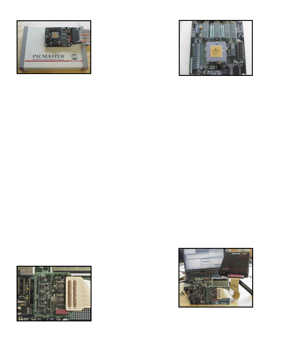
www.circuitcellar.com
CIRCUIT CELLAR
®
Issue 154 May 2003
63
or set a software breakpoint. I still
prefer having a serial port operational
for debugging, but if your project
doesn’t have the physicals (connec-
tor, RS-232 conversion circuitry,
UART, etc.) needed for a serial port,
emulation is better than trial-and-
error coding or reading a row of
makeshift debugging LEDs.
The MPLAB ICE 2000 hardware is
just one part of the equation. Before I
can do all of the wonderful debugging
and tracing things I’ve mentioned, I’ve
got to verify that the MPLAB ICE
2000 on the Florida Room bench has
the software support it needs.
I’ve already downloaded and installed
the latest spin of MPLAB, and applied
the required patch for the MPLAB ICE
2000. All of the MPLAB software on
CD-ROM was included with the
MPLAB ICE 2000 for those of you
without fast download capability.
After following the quick-start
guidelines, I thought I was ready to
been replaced by a smaller emulator
device that uses a standard 25-pin
male-to-male cable to connect the
MPLAB ICE 2000 emulator pod to the
host PC’s parallel port.
I didn’t have a laptop during the
productive life of my PICMASTER.
Even if I had owned a laptop, I could-
n’t have used it, because I wouldn’t
have been able to plug in the special
I/O card. The MPLAB ICE 2000’s
smaller size and parallel interface
make it perfect for use in the field
with a laptop PC.
The PICMASTER processor pod was
designed to hover over the target
board. A special ribbon cable connect-
ed the PICMASTER processor pod to
the PICMASTER system unit. A set of
DIP extender pins provided the clear-
ance between the PICMASTER
processor pod and the target socket on
the target board. You could also use a
ribbon cable/DIP header arrangement
instead of the extender pins for target
sockets in areas that would not allow
the PICMASTER emulator header to
fit. The MPLAB ICE 2000 uses a
smaller processor module and semi-
permanently attached cable instead of
the separate ribbon cable and emula-
tor header used by the PICMASTER.
Like the PICMASTER, the MPLAB
ICE 2000 processor pods are PIC fami-
ly type specific. They fly above the
target socket or tie in with a DIP
header/ribbon cable arrangement.
Unlike the PICMASTER, which put
the bond-out on the header at the end
of the ribbon cable, all of the PIC fam-
ily’s smarts are found in the MPLAB
ICE 2000 processor module, which
from the PICMASTER’s view, is on
the opposite side of the ribbon cable.
Instead of an emulator header, a
device adapter sits at the end of the
MPLAB ICE 2000 processor module
ribbon cable (see Photo 3). The
device adapter logically and electri-
cally connects the MPLAB ICE 2000
emulator pod and processor module
to the target socket on the target
board. In addition, the MPLAB ICE
2000 device adapter carries a special
active device to generate an oscilla-
tor clock that emulates the specifica-
tions of a real or production oscilla-
tor configuration.
Taking things one step further, an
optional transition socket can be
attached to the MPLAB ICE 2000
device adapter. The transition socket
allows the MPLAB ICE 2000 system
to be attached to targets that require
an SMT interface between the MPLAB
ICE 2000 and the target board. Photo 4
shows a fully loaded, ready-to-go
MPLAB ICE 2000 and target board.
TARGET PRACTICE
Adding the MPLAB ICE 2000 to
your PIC tool chest enables a pletho-
ra of functionality. If you’re counting
PIC instruction cycles to verify tim-
ing loops, the MPLAB ICE 2000 can
do that for you. Instead of writing
routines to track the value of a single
variable, you can employ an MPLAB
ICE 2000 to watch your variables and
file registers.
Incorporating the MPLAB ICE 2000
into your design cycle means you no
longer need to add endless loops at
desired breakpoints in your code. Use
MPLAB ICE 2000 to set a breakpoint
based on internal or external signals,
Photo 1—
This PICMASTER has ushered in medical
equipment, remote meter reading equipment, CNC
controllers, a PIC-based ’Net appliance, and even a
less powerful clone. The emulator header and ribbon
cable assembly are also shown in this shot.
Photo 2—
The bond-out IC is the heart of the emulator
header. Basically, the bond-out is a real PIC16C5x
core that enables the internals of the PIC16C5x core to
be examined by external electronics. Most of the clock
and power parameters are jumper selectable.
Photo 3—
Interesting…The two ICs you see are bond-
out ICs for the PIC12C67x family. This device adapter
and the processor module combine to replace the
PICMASTER’s emulator header.
Photo 4—
The MPLAB ICE 2000’s running lights are
green, and the PICDEM 2 Plus target is running a
slightly modified demo program. Notice the MPLAB
ICE 2000 is sitting on a tripod (it comes with the sys-
tem). That means I can pile lots of junk on my bench
under the MPLAB ICE 2000 and still be able to use
it effectively.
MPLAB ICE 2000 “H” indicator LED.
My first action was to immediately
remove power before I let the magic
smoke out of the MPLAB ICE 2000.
Instead of reading, I turned on the
MPLAB ICE 2000 and again received
64
Issue 154 May 2003
CIRCUIT CELLAR
®
www.circuitcellar.com
apply power to the MPLAB ICE 2000
emulator pod/target board rig and
scan the room for signs of smoke. I
inserted the PCM16xV0 processor
module into my emulator pod and
attached the PIC16F87xA device
adapter to the end of the PCM16xV0’s
ribbon cable. Then, I used the DIP40
extender pins to plug the device
adapter into the target board.
For now, my target board will be a
PICDEM 2 Plus demo board. The PIC-
DEM 2 Plus is set up to carry a
PIC16F877A or PIC18F452, and it has
LEDs, an LCD, switches, a thermome-
ter IC, a software-implemented real-
time clock, and a serial port. Also, I
have the example assembler source
code for the PICDEM 2 Plus test PIC
that I can run to verify the MPLAB
ICE 2000’s operation.
If the target is supplying the system
power, it’s recommended to power up
the MPLAB ICE 2000 before applying
power to the target. So, I attached the
MPLAB ICE 2000 power brick and
fired up the MPLAB ICE 2000. I
immediately got a red light on the
Photo 5—
This can get as busy as you want. When I’m in a bind, I use one window’s contents to help me with another
window’s information. If it gets to be too much, just click and print the window contents to a file or your printer.
Visit us on the web www.jkmicro.com
Call 530-297-6073 Fax 530-297-6074
512K Flash plus DIP socket to accept an M-Systems DiskOnChip.
Development systems contain necessary hardware and software tools for fast development.

66
Issue 154 May 2003
CIRCUIT CELLAR
®
www.circuitcellar.com
the red LED. OK, it was time to con-
sult the documentation.
As it turned out, the “H” LED is a
halt LED. To me, a red indicator on a
status panel usually means bad
things, but not that time. I’d done
nothing in the way of device or
MPLAB ICE 2000 configuration at
that point, so the active halt LED was
a good thing and wasn’t going to set
off the Florida Room’s smoke detec-
tor. I’d crawled pretty far forward
without incident, so with a bit more
confidence, I started the new MPLAB
IDE, and powered up the MPLAB ICE
2000 and PICDEM 2 Plus.
The new MPLAB IDE supports a
number of debuggers, including the
“hockey puck” (i.e., MPLAB ICD 2),
the MPLAB simulator, and the
MPLAB ICE 2000. After selecting the
MPLAB ICE 2000, I was warned that,
if this was my first time, I needed to
load a parallel port driver for
Windows 2000. I remember clicking
through some warnings when I
installed the MPLAB IDE software.
Something told me that I should have
paid attention to them as I clicked
through. Fortunately, the MPLAB IDE
directory “Drivers2000” was a pretty
obvious choice and inside was an
Photo 6—
The label
there
signifies the end of the
delay_1s
routine timing capture. Everything before the
there
label begins at the
here
label. There are two
call delay
instructions back to back. Notice how the
second
call delay
begins at line two, and the first
call delay
ends at line negative two.
· RS232 or TTL Serial ports
· Parallel port
· 2MB/4MB onboard memory
· GPIO
· EPROM + Flash Memory
use X86 for Microprocessor in:
· Traffic Control Systems
· Automation and Industrial Applications
· Real-ime Network Appliances
Tel: 1-626-444-6666 email:info@icoptech.com
Tel: 886-2-8990-1933 email: info@icop.com.tw
Tel: 81-3-3265-1508 email: info@icop.co.jp
Tel: 86-755-2661-1770 email: info@icop.com.cn
For applications and technical information, check www.dmp.com.tw/tech/
www.circuitcellar.com
CIRCUIT CELLAR
®
Issue 154 May 2003
67
HTML file that detailed the parallel
port driver installation.
After completing the parallel port
driver installation, I selected the
MPLAB ICE 2000 as my debugger
and fired the MPLAB ICE 2000 and
PICDEM 2 Plus target. Once again,
the halt LED went active but with-
out the “where’s the emulator?”
error message. The PICDEM 2 Plus
wasn’t showing any signs of trouble,
so I decided to create a project based
on the PICDEM 2 Plus PIC16F877
test code.
The project-generation process for
the new MPLAB IDE involves defining
how you want your project’s environ-
ment to operate, selecting a PIC
device, and specifying the location of
your project files. After all of that is
defined, files are added to the project
workspace, and the configuration for
the selected PIC is established.
I initiated a project that I named
“Circuit_Cellar.” The PICDEM 2 Plus
test code source was written in PIC
assembler, and I specified my language
tool suite as Microchip MPASM. You
already know my target PIC was a
PIC16F877A, and with that selection I
set the PIC configuration fuses while I
was in the Configure pull-down menu.
The next step was to tell the
MPLAB IDE and MPLAB ICE 2000
that I would be powering the MPLAB
ICE 2000 from the target PICDEM 2
Plus demo board and that the target
board would be supplying the micro-
controller clock. The MPLAB IDE
makes the necessary menu items
available as you tell it what you
want to do. After I informed the
MPLAB IDE that I wanted to power
the MPLAB ICE 2000 from the tar-
get, it freed the check box to allow
me to select an internal or external
clock source.
Normally, at that point I would
have created my source files and
added them to my Circuit_Cellar
project’s workspace. Because the files
already existed, all I had to do was
add them to their respective cate-
gories. For instance, all of the PIC-
DEM 2 Plus source files were added
to Source Files and the linker
script—16F877.lkr—was pushed into
the Linker Scripts slot.
After everything was in place, I
executed a Build All. Because I didn’t
write the code, I wasn’t expecting
any surprises, and I didn’t get any.
The PICDEM 2 Plus test code com-
piled and linked without a hitch. I
clicked on Run and the PICDEM 2
Plus LCD put up the Voltmeter
Photo 7—
The flip-flop target board supplies power and
a clock. The device adapter hovering above the flip-flop
is emulating a PIC16F877A. Data and power to the
NICki flow across the three ribbon cables. A laptop
computer is running MPLAB IDE and providing the ping
commands via an Ethernet crossover cable.

68
Issue 154 May 2003
CIRCUIT CELLAR
®
www.circuitcellar.com
menu item. It asked me to
press the RA4 button for
the next menu item or hit
the RB0 button to start the
voltmeter application seg-
ment. I took a snapshot of
the MPLAB IDE various
view windows to give you
an idea of what the MPLAB
IDE/MPLAB ICE 2000 emu-
lation system can show you
(see Photo 5).
The MPLAB ICE 2000 has
quite a few more tricks up
its ribbon cable. Advanced
complex triggering functions
allow you break a program
using software and hardware
triggers. You can break and
debug your program using
events, sequences of events,
and even the bits inside a
data memory byte.
The Time Between Events
function can use symbolic,
binary, or hexadecimal nota-
tion to define start and stop
points in the program code.
A timestamp in the Trace
window gives the elapsed
time between the starting
and ending addresses. I was particular-
ly interested in this feature and
checked out the accuracy of the real-
time clock delay routines in the PIC-
DEM 2 Plus test code.
I didn’t get the answers I was
expecting. I was timing a 1-s delay
loop and getting back 0.19 s as the
elapsed time. After spending a couple
of hours trying to figure out if I really
knew how to read the elapsed time in
the trace window, I decided to check
the PICDEM 2 Plus source code to
see if the oscillator frequency
matched my 20-MHz oscillator can
that was mounted in the PICDEM 2
Plus demo board’s Y2 socket. Aha!
The PICDEM 2 Plus test software
was written for a 4-MHz clock.
Now, I can show you the Trace
window result, which reads out an
elapsed time of 0.984846000 s. You
can see this result in Photo 6. To get
this timing measurement, I simply
added a
here and there label
between the points I wanted to
measure in the PICDEM 2 Plus
source code:
here
call delay_1s
there
Just in case you’re wondering about
that mass of cables protruding from
under the LED indicators on the
MPLAB ICE 2000 in Photo 4, they’re
called logic probes, which are yet
another way to introduce break and
debug points. There are three color-
coded sets of wire probes. The gray
probes are TRGIN, TRGOUT, and
HLTOUT. The TRGIN, or trigger in
probe, is an active high or edge-trig-
gered input used to freeze the trace
buffer without halting the processor in
Logic Level mode. In Edge-Triggered
mode, the TRGIN probe freezes the
trace buffer and halts the processor.
TRGOUT, or trigger out, is used to
trigger external devices such as oscil-
loscopes at selected points in the pro-
gram. HLTOUT signals that the
processor is halted (high logic level) or
running (low logic level). The
logic probe set can also supply
5 V at 250 mA on the red
probe with the black probes
acting as ground points. The
white logic probes represent
8 bits of external input
trace/trigger input. You can
use these pins to execute
break and debug points on the
target’s I/O pins.
SPEAKING RUSSIAN
Well, not yet in Arizona
anyway. Now that you have
been exposed to the usefulness
of the MPLAB ICE 2000, how
about if I show you how you
can use it to perform crude
protocol analysis? What does
this have to do with the
Russian language? Nothing.
It’s just that the target board is
called NICki, and that sounds
Russian enough for me.
NICki is a CS8900A-based
microcontroller network
interface card (NIC). Although
I just called NICki the target
board, NICki is in fact the
Ethernet communications
port for a couple of specialized target
boards. The primary target board,
which is called flip-flop, is based on
the PIC16F877 on one side and our
MPLAB ICE 2000 acting as a
PIC16F877A in a 40-pin DIP package
on the flipside. I won’t use the
PIC16F877 side of flip-flop, because
it’s already populated with a TQFP
version of a PIC16F877.
Flip-flop is simply a device adapter
that takes the MPLAB ICE 2000’s 40-
pin DIP extender pin set and routes
the signals to an array of standard 0.1
″
10-pin headers. The 10-pin headers on
the flip-flop allow IDC-terminated
ribbon cable to carry the emulated
PIC16F877A signals to another cus-
tom device adapter that’s pinned to
accept the NICki Ethernet module.
With this arrangement, I can develop
and debug code for both the NICki3
(i.e., the 3.3-V version of the
CS8900A) and the NICki5 (i.e., the 5-
V version of the CS8900A), because
the flip-flop can supply either 3.3 or
5 VDC at the flip of a switch. Flip-flop
ARP REQUEST
FROM:
HARDWARE ADDRESS - 00 10 A4 8E 56 3B (LAPTOP MAC ADDRESS)
IP ADDRESS - C0 A8 00 08 (192.168.0.8 LAPTOP IP ADDRESS)
TO:
HARDWARE ADRESS - UNKNOWN NICki MAC ADDRESS
IP ADDRESS - C0 A8 00 96 (192.168.0.150 NICki IP ADDRESS)
PACKET BEGINS AT OFFSET 0032
0000 -- 5B 2B 1F 6E 00 1C FF 01 00 00 06 00 00 00 00 -[+.n... ........
0010 00 00 00 00 00 00 00 00 00 00 00 00 00 00 00 00 ........ ........
0020 00 3C 01 38 00 06 C4 A3 68 69 00 00 00 80 00 00 .<.8.... hi......
0030 00 3C FF FF FF FF FF FF 00 10 A4 8E 56 3B 08 06 .<...... ....V;..
0040 00 01 08 00 06 04 00 01 00 10 A4 8E 56 3B C0 A8 ........ ....V;..
0050 00 08 00 00 00 00 00 00 C0 A8 00 96 00 00 00 00 ........ ........
******************************************************************************************
PING REQUEST
FROM:
HARDWARE ADDRESS - 00 10 A4 8E 56 3B (LAPTOP MAC ADDRESS
IP ADDRESS - C0 A8 00 08 (192.168.0 8 LAPTOP IP ADDRESS)
TO:
HARDWARE ADDRESS - 00 00 45 44 54 50 (NICki MAC ADDRESS - "EDTP")
IP ADDRESS - C0 A8 00 96 (192.168.0.150 NICki IP ADDRESS)
PACKET BEGINS AT OFFSET 0032
0000 -- B1 02 1F 7C 00 1C FF 01 00 00 06 00 00 00 00 -...|... ........
0010 00 00 00 00 00 00 00 00 00 00 00 00 00 00 00 00 ........ ........
0020 00 4A 01 38 00 06 B8 A3 68 69 00 00 00 80 00 00 .J.8.... hi......
Figure 1—
You can take the PIC memory dumps and analyze a packet byte by
byte right down to the flags and checksums.
www.circuitcellar.com
CIRCUIT CELLAR
®
Issue 154 May 2003
69
With power wrapped in simplicity, the
MPLAB ICE 2000 and the new MPLAB
IDE prove that it doesn’t have to be
complicated to be embedded.
I
also carries a crystal and some LEDs
just in case you need them. NICki and
her comrades are shown Photo 7.
For developing code based on
Ethernet protocols, it’s good to have a
packet analyzer that can give you a
view of what’s entering and exiting as
Ethernet I/O. If you don’t have a pro-
tocol analyzer, you can use the
MPLAB ICE 2000 to view incoming
and outgoing packet structures.
I’ve written the NICki code to allow
a limited payload packet to be assem-
bled as an array in the PIC16F877A
data memory. After the program has
assembled the packet (incoming or
outgoing), I can set a break point at the
final packet assembly point and use
the MPLAB ICE 2000 File Registers
window to view the PIC16F877A data
memory that contains the packet
array. Each byte has to be in a certain
order and structures like IP addresses
and data areas can be seen easily using
this method.
An example of an ARP request and a
ping request captured by the MPLAB
ICE 2000 break points are shown in
Figure 1. In the ARP request portion of
Figure 1, note the broadcast address (FF
FF FF FF FF FF) followed by the sender’s
hardware address (MAC address), which
is immediately followed by 0806 signi-
fying an ARP request. At that point, the
laptop doesn’t know NICki’s IP address.
You can pick up the laptop’s IP address
beginning at offset 004E (C0 A8 00 08).
The ping request contains both the
MAC address of NICki gained via the
ARP request (00 00 45 44 54 50) plus
NICki’s IP address (C0 A8 00 96). The
data area begins with the lowercase
alphabet string.
EXIT LOOP
All of the examples I have presented
here have been assembler-based. The
MPLAB ICE 2000 is capable of execut-
ing and debugging files generated by
PIC C compilers, as well. The CCS C
compiler that I use was not listed as
one of the predefined MPLAB ICE 2000
tool suite compilers; however, a quick
visit to the CCS web site solved that
problem. I simply downloaded and
installed the MPLAB 6.x plug-in and
the CCS PIC C compiler on my PC was
automatically registered with MPLAB.
SOURCES
PIC C compiler
CCS, Inc.
(262) 797-0455
www.ccsinfo.com
CS8900A Ethernet LAN controller
Cirrus Logic, Inc.
(512) 851-4000
www.cirrus.com
MPLAB ICE 2000, PICDEM 2 Plus
demo board
Microchip Technology, Inc.
(408) 792-7200
www.microchip.com
Fred Eady has more than 20 years of
experience as a systems engineer. He
has worked with computers and com-
munication systems large and small,
simple and complex. His forte is
embedded-systems design and com-
munications. Fred may be reached at
fred@edtp.com.

70
Issue 154 May 2003
CIRCUIT CELLAR
®
www.circuitcellar.com
or the experi-
menter, one thing
that has not gotten
less expensive to imple-
ment is the user interface, or the front
panel. Although modern solid-state
components have become inexpensive,
switches, potentiometers, keypads,
and the like have not. One exception
is parallel alphanumeric LCDs, which
cost only about $10 if you get them
from surplus outlets, many of which
advertise in Circuit Cellar.
I often use matrix-type keypads—the
common 12-key types—designed for
telephones; however, I generally don’t
have enough buttons. Membrane-type
keypads, which allow you to add your
own legends, are nice but expensive.
My old favorite, the Grayhill 83BB1
16-button keypad, works well, but it
too is getting pricey.
The other problem involved here is
the number of host MCU I/O port lines
consumed by the user interface. Merely
using a 16-button keypad and an LCD
requires 14 lines (a few less if you clev-
erly share some of the keypad lines with
the LCD). Another complication is that
the matrix keypad must be scanned in
software to detect when a button is
pressed. Depending on the functions of
these buttons, this scanning may have
to occur frequently, which may affect
the ability of the host MCU to per-
form other time-critical functions.
To overcome these two problems, I
decided to design a front-panel interface
using the most reasonably priced parts
I could find. The LCD is a common 4 ×
20 display that costs about $8. The key-
pad is an RCA universal infrared remote
control that you can buy for less than it
would cost to obtain a decent 16-key
matrix keypad. Both of these devices
are controlled by an inexpensive Atmel
AVR microcontroller, the AT90S2313.
The AT90S2313 microcontroller ulti-
mately links to your host MCU via a
two-wire 1200-bps serial link.
To make the unit a bit more versa-
tile, I allowed for software control of an
LED backlight for the LCD. Inexpensive
LCD units don’t often include such a
backlight, but the more expensive mod-
els do. I also included provisions for
an optional power on/off control of
the main circuit via the On/Off but-
ton on the infrared remote control.
One idea I had in the back of my
mind when designing this was the pos-
sibility of building several different
pieces of bench test equipment all uti-
lizing a similar front-panel concept,
thereby allowing one infrared remote
control to service numerous devices.
The only problem was that I had already
built several such devices conventional-
ly before this idea came to mind.
Figure 1 is the schematic diagram of
the interface. In the diagram, you don’t
see a 5-V power supply, which is need-
ed to run the circuit. I assume the 5-V
supply would be available from the
main circuit. Should you choose to
control the main unit using the remote
control’s On/Off button, you would
need to add a small, independent 5-V
power supply to serve this unit.
The LCD is operated in the com-
monly used 4-bit mode, which allows
Poor Man’s Front Panel
f
Not every design
problem requires a
complicated, expen-
sive solution. For
instance, you don’t
have to lose your mind
and wallet the next
time you find yourself
scrounging for a front
panel. In this article,
Brian shows you how
to maximize your time
and money.
Brian Millier
SHORT
SOLUTION
Control button pressed
ASCII code
CURS LEFT
28
CURS RIGHT
29
CURS UP
30
CURS DOWN
31
PREV CH (Backspace)
8
Table 1—
ASCII code is sent to the host when the con-
trol buttons are pressed on the infrared remote control.
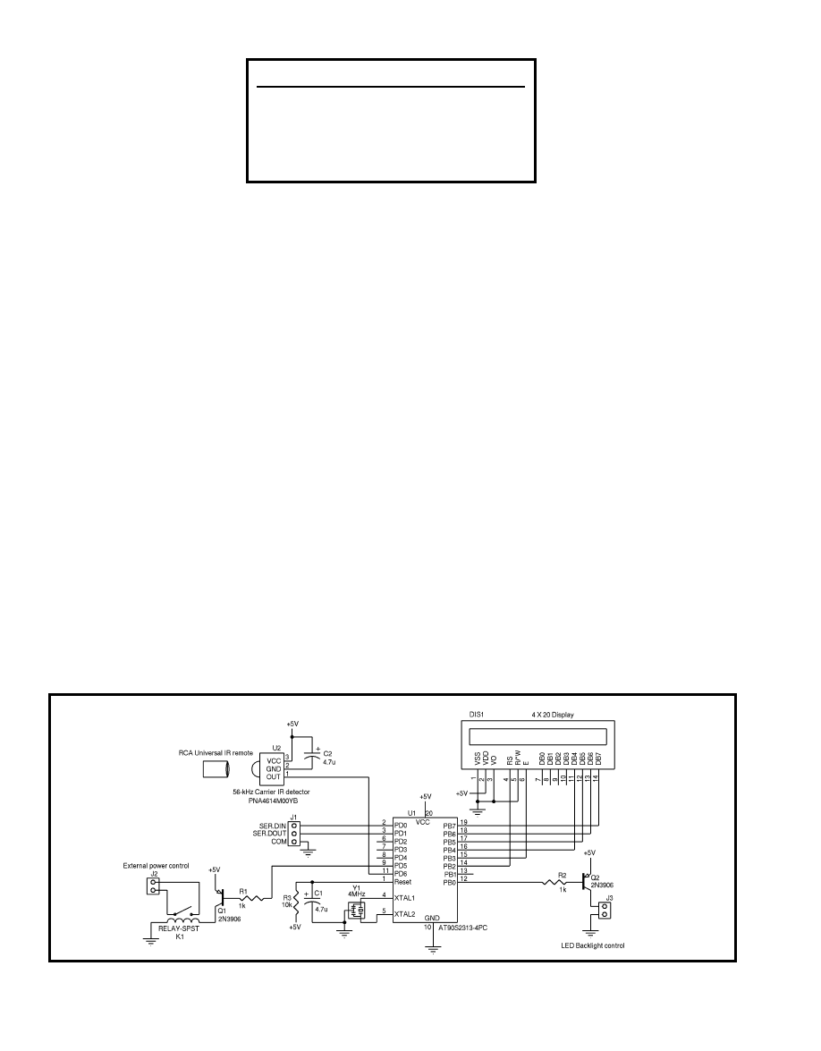
www.circuitcellar.com
CIRCUIT CELLAR
®
Issue 154 May 2003
71
the PREV CH (i.e., previous char-
acter) button as a Backspace key.
FIRMWARE
The firmware is in a constant
loop looking for activity from the
infrared remote control. When it
sees activity, the firmware enters
a routine that decodes the IR code
into a 12-bit integer (only 8 bits
are actually used). The firmware trans-
lates this number into the proper ASCII
code and sends it out the serial port (at
1200 bps) to the host microcontroller.
Table 1 shows the ASCII codes for con-
trol of the cursor and backspace buttons;
all other buttons use standard ASCII
codes, which need not be repeated.
While the software is in this loop,
it also checks for incoming serial data
from the host. Upon receiving charac-
ters, it either displays a character on
the LCD or performs some other dis-
play function such as Clear Screen or
moves the cursor.
In the case of the numeric buttons
and decimal point, the keystrokes are
also echoed locally on the LCD, at the
current cursor location. This reduces the
workload on the host. The firmware can
send messages/parameters to set up the
LCD screen. Then, it can watch for
infrared remote cursor control button
codes to track which parameter has
your “focus,” and then move the cursor
to that parameter and collect the ASCII
string representing the number that
you’re entering on the remote control.
it to be easily controlled using
only six of the AT90S2313’s
port lines. A small infrared
detector module (this must be a
56-kHz carrier type) is coupled
to the port D6 line of the
AT90S2313. I had a Digi-Key
module (part no. 160-1162) on
hand, so that’s what I used.
Although that part is no longer
available, the Panasonic
PNA4614M00YB or Jameco 176541
should work just as well.
Two additional port lines were used
to drive 2N3906 transistors to supply
LED backlight current and to drive a
small relay for optional external power
control. I used an inexpensive 4-MHz
ceramic resonator for the AT90S2313’s
clock, because this is accurate enough
for use with a 1200-bps serial data link.
The AT90S2313 contains a full-
function UART, which is critical in
this application because it would be
impossible for it to monitor the serial
bitstream coming from the infrared
remote control and also monitor the
serial data coming from the host
microcontroller, which contains the
LCD commands and data.
As a member of Atmel’s flash memo-
ry-based AVR microcontroller family, the
AT90S2313 is easy to program. All you
need is a simple cable connected to a PC
printer port and the right software. Note
that I didn’t show the programming
header connections in Figure 1. I suggest
using BASCOM-AVR compiler program-
ming software from MCS Electronics.
This software contains wiring details in
its help file. You can download a free
demo version of the BASCOM-AVR
compiler, which can handle the small
program needed for this project. For
more information on programming, you
can read my article, “My fAVRorite
family of Micros” (Circuit Cellar 133).
The firmware is written in BASCOM
AVR BASIC and fits in the AT90S2313’s
2-KB flash program memory. Because I
had to write the routines to decode the
infrared remote control codes, I spent
time examining the different infrared
coding schemes available on my RCA
universal remote control. Many of
them are complex. I ended up choosing
the Quasar TV mode (#054 on my RCA
universal remote) because it was easy
to decode in software. This allowed me
access to the 10 numeric buttons, four
cursor control keys, and the Enter and
On/Off buttons. The following keys
(and the use that I assigned to them) are
also available: Mute and PREV CH. For
the former, I added a dot on the button
and use it as a decimal point. I defined
Figure 1—
An Atmel AVR—the AT90S2313—handles the LCD, infrared remote control, and host interface duty in this design. Also shown are optional control circuits for back-
light control and on/off control of the main circuitry via the remote control’s On/Off button.
ASCII code
Command
128
Clear screen
144–183
Define cursor
x position (144 = 0, 183 = 39)
192–195
Define cursor
y position (192 = line 1, 195 = line 4)
208
Move cursor to location as defined
240
Backlight off
241
Backlight on
Table 2—
The host microcontroller controls the LCD with a set of commands.
www.circuitcellar.com
CIRCUIT CELLAR
®
Issue 154 May 2003
73
Host echoing of your numeric input to
the LCD is not necessary, as I explained
earlier. The Backspace key function
works locally on the LCD as well.
Pressing the On/Off button on the
remote control will toggle the optional
power relay on and off. It does not
send any message to the host.
Table 2 is a list of commands that the
host can issue to control various aspects
of the LCD. Note that all commands are
mapped to the upper 128 ASCII codes,
and are only one-character long. Also
note that the parameter is embedded in
the command itself. To send an ASCII 96
character to the LCD, you merely send
the appropriate ASCII code. The LCD is
fast enough to display characters sent to
it at 1200 bps, but you might want to
allow for some delay in your software
when issuing the Clear Screen command,
because it takes the LCD a while to do
this. To move the cursor, send out the
appropriate command for the x and y
locations, and then send an ASCII 208
character to move to that position.
I defined six special block graphics
characters (ASCII codes 1–6). ASCII
code 1 is a blank character, and the other
five are blocks of one to five column
widths, respectively. These could be
used for horizontal bar graph displays.
However, the LCD itself has a small
space between consecutive character
positions on the screen, so the resulting
bar graph is not aesthetically pleasing.
The source code for the firmware is
available on the Circuit Cellar ftp
site. You can make changes to suit
your own applications. For example,
you could change the data rate or use
a different size LCD depending on
your application’s needs.
I
PROJECT FILES
To download the code, go to
ftp.circuitcellar.com/pub/Circuit_
Cellar/2003/154/.
Brian Millier is an instrumentation
engineer in the Chemistry Depart-
ment at Dalhousie University in
Halifax, Canada. He also runs
Computer Interface Consultants. You
may reach him at brian.millier@dal.ca.
RESOURCES
Infrared detector modules
176541
Jameco Electronics
(800) 831-4242
(650) 592-8097
www.jameco.com
PNA4614M00YB
Panasonic
www.panasonic.com
SOURCES
AT90S2313, data books, Assembler,
simulator
Atmel Corp.
(714) 282-8080
www.atmel.com
BASCOM-AVR Compiler/programmer
MCS Electronics (Holland)
+31 75 6148799
www.mcselec.com
LCD
Timeline, Inc.
(310) 784-5488
www.timeline-inc.com/lcd.html
74
Issue 154 May 2003
CIRCUIT CELLAR
®
www.circuitcellar.com
ack in 1970s,
the Gerber Scientific
Instrument’s vector
photoplotter helped
make possible the inexpensive pro-
duction of large color television
screens. This technological break-
through helped the name “Gerber”
become synonymous with computer-
aided manufacturing (CAD/CAM).
And from this grew the de facto inter-
national standard file format for plot
data—the Gerber format.
How does one company’s file format
become universally accepted? The
word “simplicity” sums this up nice-
ly. Many companies bury their for-
mats in proprietary and machine-only
readable hieroglyphics, but the Gerber
format uses an ASCII text format
allowing it to be viewable (and
editable) in standard text editors.
This has significance for designers
because PCB manufacturers require
plot files of your PCB designs in
order to fulfill your needs. One of the
requirements is a high-contrast film of
each PCB layer (i.e., top circuitry, bot-
tom circuitry, component silkscreen,
etc.). Each step in the process requires
adding new information to the PCB
under fabrication, beginning with
drilling and plating holes, etching top
and bottom copper layers, adding lay-
ers of plating, solder mask, and silk-
screening to each side of the board.
Producing the necessary films is a
photographic process that has changed
over the years. We’ve come a long
way since the days of scratching out
schematics on paper. Juggling parts
positions is like pushing around furni-
ture shapes on a room-sized grid until
they fit within a PCB outline. And
building each of the necessary PCB
layers by hand involved laying down
black tape on a translucent Mylar
material. These taped artworks (lay-
ers) were usually produced at two
times life size. When photographical-
ly reduced to the final size, overall
placement errors were also reduced by
50% and a positive/negative film of
the layer was produced for the PCB
fabrication house.
With the introduction of the pho-
toplotter (and PCB layout applica-
tions), hand taping has become a lost
art—or at least one traded in for
computer skills. Photoplotters are
the means of obtaining positive/neg-
ative films using Gerber files regurgi-
tated by PCB layout applications.
VECTOR PHOTOPLOTTER
The vector photoplotter is based on
the table or drum-type x-y plotter.
Instead of drawing with ink on paper,
the photoplotter uses light on photo-
graphic film. The light can be inter-
rupted by a shutter (like the one on a
Making Sense of the
Gerber File Format
b
Jeff
enjoys
writing
reviews
about the
devices that affect
his daily engineering
routine. This month,
he covers the story
of photoplotter tech-
nology. Read on as
he makes sense of
the Gerber “plot.”
Jeff Bachiochi
FROM THE
BENCH
Figure 1—
The vector photoplotter requires numerous
mechanical modules to project a selected aperture at
precise coordinates. Exposure to the photographic
film can be flashed or drawn depending on whether
the light source is standing still or moving with
respect to the film.
Film
Light source
Optics
Aperture wheel
Shutter
Optics
X-Y table

www.circuitcellar.com
CIRCUIT CELLAR
®
Issue 154 May 2003
75
camera) and doesn’t have to turn on
and off. This mimics the pen’s up and
down motion on the x-y plotter.
Although the x-y plotter changes
pens to draw a different color or
change the width of a line, the photo-
plotter does this by changing aper-
tures. An aperture is a tiny slide
(directly in the light path) that proj-
ects an image on the film. Apertures,
which come in all sizes and shapes,
are held in a carrousel, making it easy
for one to be inserted into the light
path (see Figure 1). [1]
There are two types of apertures,
one for drawing lines and another for
flashing a pattern such as a compo-
nent pad. Because the exposure time
for each type is different, separate
apertures (with different filter materi-
al) are used to flash and draw an aper-
ture of the same shape and size using
the same light source. Minimal con-
trol information is necessary to oper-
ate this opto-mechanical system.
Enter the Gerber file format.
COMMAND CODES
Because the Gerber format is an
ASCII-based file format, commands
are easily identified (usually a single
letter). Commands are grouped into
five categories: light control (D), com-
mand interpretations (G), movement
control (X and Y), arc control (I and J),
and machine control (M).
Each command or block (i.e., a group
of commands) ends with an ASCII *
character (followed by an optional CR
LF). The photoplotter acts on each
command (or group) after the * has
been received.
Gerber files generally start with G
codes (see Table 1). These commands
tell the photoplotter how to handle
the data it will receive. To imprint
anything on the photographic film,
the light source needs to be con-
trolled. D codes are used not only to
handle the light source (in reality the
shutter), but also to choose the aper-
ture (see Table 2).
The first few D codes are reserved
for shutter control. Shutter control
eliminates the need to turn the light
on and off, which would shorten the
life of the bulb. With a vector photo-
plotter the number of useable aper-
tures is limited by the size of the car-
rousel. Apertures are arranged in any
order on the carrousel; however, this
order must match the separate aperture
list produced by the PCB layout appli-
cation (RS-274D, more on this later).
Now that you can illuminate the
photographic film, the next codes are
needed to move the light source (or
head) around to precise locations on
it. X and Y codes are coordinate pairs
indicating a two-dimensional posi-
tion. A reference position (usually
the lower left corner of the system)
is designated as 0,0 (X = 0 and Y =
0). Absolute positioning (G90) calcu-
lates movement relative to the refer-
ence position 0,0. Relative position-
ing (G91) calculates movement rela-
tive to the last position. Independent
of the type of positioning (G code),
the path the head takes to its next
position is also based on previous G
codes. The Normal mode (G01) will
be the shortest path or straight line;
however, your design may use
rounded corners or other arc-type
drawing requirements.
G codes (G74 and G75) alter the
path the head will take between two
points. When drawing arcs, an addi-
tional set of coordinates is needed
(I/J). The I/J coordinates are used to
calculate the radius of the arc.
Depending on the last arc code (G74
or G75), the position of I/J also
determines how many degrees of arc
will be drawn (up to 90° for G74 and
360° for G75).
X and Y (as well as I and J) are neb-
ulous commands similar to aperture
D codes. I’ve indicated how aperture
positions do not have an implied size
or shape associated with them and a
separate aperture list must accompa-
ny the Gerber file (RS-274D). The
X/Y position values do not have an
implied scale. A number like 1000
could be 1000
″
, 0.1
″
, or 10 mm for
that matter! In its quest for simplicity
the decimal point was left off. In fact,
the values used can indicate any
amount of precision (up to six inte-
gers and six decimal places).
The values used (in the X, Y, I, and
J commands) have a format that, like
the aperture sizes and shapes, must be
given to the photoplotter operator,
because they are not part of the com-
mand structure. Often, a comment
line at the beginning of the file will
hold this information in some non-
standard form like G04 2,4,NZ, inch-
es* (the beauty of ASCII file format).
In this case the 2,4 means two inte-
ger positions followed by four deci-
mal positions or an xx.xxxx format.
G Code
Command interpretation
What happens
G01
Future X/Y commands are straight-line moves
Movement from X/Y to X
l
/Y
1
will be the short-
est distance (straight line)
G02
Future X/Y commands are clockwise arcs
Movement from X/Y to X
l
/Y
l
will be in an arc
clockwise using I/J as the arc center
G03
Future X/Y commands are counterclockwise arcs
Movement counterclockwise using I/J as the
arc center
G04
Ignore these comments
Comments for documentation purposes are
not commands to be executed
G54
Prepare to change apertures
The mechanics of changing apertures
requires preliminary work, so get ready
G74
Future arcs are quadrant arcs
Arc movement will be up to 90°
G75
Future arcs are full 360° arcs
Arc movement will be a full circle
G90
Absolute data
Movement is based on a reference coordi-
nate of 0/0
G91
Incremental data
Movement is based on the last coordinate
location
Table 1—
G codes allow data to be interpreted in many ways. Although G codes are used to set up the initial com-
mand interpretations, they may occur anywhere in the file.
Table 2—
Carrousels accommodate 24 different
replaceable apertures. This is a physical limitation for
the vector photoplotter carrousel.
D code
Command interpretation
D01
Open the shutter
D02
Close the shutter
D03
Flash the shutter (open then close)
D10-up
Use aperture in this position on the
carrousel
76
Issue 154 May 2003
CIRCUIT CELLAR
®
www.circuitcellar.com
The measurement system is in inches
without zero suppression.
File compression is always a popu-
lar subject, especially when dealing
with long downloads. Nowadays we
don’t think much about it, because it
is employed automatically
in many transfers. Back
when punch cards were the
only method of file trans-
mission, the use of short-
cuts to reduce a file’s
length were welcome not
only by the keypunch oper-
ator, but also the keeper of
the cards. Then came paper
tape files. Paper tapes were
much easier to handle, but
they still required the same
input; therefore, shortcuts
still made sense.
Zero suppression is a way
to shorten the number of
characters needed to dis-
play a value. An NZ value
of
X001500 (00.1500)
could be shortened to
X1500 with leading zeros
(LZ) suppressed or
X0015
with trailing zero (TZ) sup-
pression. In addition to
zero suppression, modality
in the command’s format
could squeeze a file’s size
even more. Modality
involves the ability to
eliminate redundant data.
For instance, Listing 1
includes the commands to
draw a line connecting three points.
Note how they can be shortened.
Using LZ and modality can save
approximately 50%. Today, with fast
transmission speeds and relatively
small files compared to other appli-
cations, these kinds of shortcuts are
unnecessary—although you can still
use them.
The final category of codes is
implemented based on the mechani-
cal needs of many vector photoplot-
ters. The M codes directly affect the
status of the system. The few M
codes in the Gerber format include:
M00 (a full machine stop), M01
(pause), and
M02 (end of plot).
Generally, you will only find
M02
used at the end of the file.
VECTORING
After the vector photoplotter’s aper-
ture carrousel has been loaded with
the appropriate apertures at each D
code position, and the photographic
film has been placed on the plotter’s
drawing surface, the system is ready
to receive your plot file. The vector
photoplotter reads each Gerber com-
mand and carries out each operation
one command at a time. The process
of changing apertures, opening and
closing the shutter, and moving the
head around to the proper coordinates
all happens based on the Gerber file
commands. You can imagine what
happens when an aperture has been
inserted into the carrousel at the
wrong position. I’ve seen plenty of
film processed with a giant trace oblit-
erating the rest of the artwork or pads
of the wrong shape. Even if a smart
designer places an aperture list as
comments in the Gerber file, there’s
still the possibility of human error
when setting up the carrousel.
RASTER SCAN
An alternate method of drawing
artwork (or anything else for that
matter) is by the raster
scan process. Whereas
vector drawing is done
object by object, raster
drawing is based on the
whole, which has been
rasterized (serialized).
Raster plotting is drawn
from raster data, line by
line (as a image is painted
on a TV screen). Artists
create art by the vector
method and would be hard
pressed to create a sketch
by the raster method;
however, there are advan-
tages for a photoplotter to
draw using rasterized data
(see Figure 2). First, there
is no need to change aper-
tures, because the light
source needs to be only
one size—the system’s
resolution or distance
between scan lines.
Second, there is no need
to have separate apertures
for flash and draw,
because all scans are
drawn. (Pads and traces
become part of the raster-
ized data and are no
longer separate entities.)
Draw (D01)
Flash (D03)
Figure 2—
The raster photoplotter has fewer mechan-
ics thanks to the computer used to translate your
Gerber file into a rasterized picture. The plotter exposes
the film in raster fashion without the need to change
apertures. You can review the complete Gerber plot
before it’s converted and sent to the plotter.
AS (optional)
FS (required)
MI (optional)
MO (optional)
OF (optional)
SF (optional)
Directive
Axis select
Format statement
Mirror image
Mode
Offset
Scale factor
Command interpretation
Match data axis to plotter axis
(A = X, B = Y)
(no)
IN-inches or MM-millimeters
(IN)
Layer plotter axis offset from data
(A = 0, B = 0)
Plotter scale to data scale
(A =1.0, B = 1.0)
Comment (default)
IJ (optional)
IN (required)
IO (optional)
IP (optional)
IR (optional)
PF (optional)
Image
Image justify
Image name
Image offset
Image polarity
Image rotation
Plotter film
Command interpretation
(no)
Plotter axis offset from data
(A = 0, B = 0)
Positive and negative
(positive)
Degrees
(0)
Comment (default)
AD (required)
AM (optional)
Aperture
Format statement
Mirror image
Command interpretation
(no)
Comment (default)
LN (optional)
LP (optional)
KO (optional)
SR (optional)
RO (optional)
Layer-specific
Layer name
Layer polarity
Knockout
Step and repeat
Rotate layer
Command interpretation
Identifies layer
Positive and negative
(positive)
Create a matrix of images
(A = 1, B = 1)
(none)
Comment (default)
IF (optional)
Miscellaneous
Include file
Command interpretation
Figure 3—
Extended Gerber data commands deal with how the data is handled. It
helps to automate the process so you don’t have to enter external data, like aper-
ture size and type.

www.circuitcellar.com
CIRCUIT CELLAR
®
Issue 154 May 2003
77
The elimination of the aperture car-
rousel and the use of a laser as the light
source for drawing on the photographic
film reduce the mechanics of the raster
photoplotter. The simplicity of the
laser photoplotter is based on a com-
puter, which must transform the vector
Gerber data into rasterized data. Once
again, there are advantages to using an
interim computer as a link between the
Gerber data file and the raster plotter.
Because the Gerber data must be
entered into the rasterizer, a by-product
is the display of the artwork image on
the computer screen. You can review
each plot before it is cast in stone, er,
film. This saves time and money by
not plotting and developing artwork
film with obvious errors.
RS274-X
Without altering the basic data of a
Gerber file (RS274-D), it was possible
to add additional system instructions
(mass parameters) to the file, creating
RS274-X or extended Gerber data.
Now a Gerber file could have all
those extra goodies, like aperture
information, which totally eliminated
the potential for human error.
The extended data can be grouped
into five functions: directives, image,
aperture, layer-specific (not PCB
layer), and miscellaneous. Extended
data must conform to the RS274-D
format, which means each block
(group of commands) must end with
the end-of-block (EOB) character (*).
In addition, the extended data format
character (%) must surround each
group of extended functions (sort of
like an envelope holding all of the
extended data). If you review
Figure 3, you’ll see that extended
Gerber data has to do with handling
the data and not defining it.
Many of these optional commands
deal with special circumstances that
are beyond the scope of this article;
however, it is worthwhile to look at
the three required commands. The FS
command is responsible for specify-
ing the format of the X, Y, I, J coordi-
nate data, as well as indicating zero
suppression. Coordinate data format
is in the XidYid format, where i is
the number of integer digits and d is
the number of decimal digits (i.e.,
X24Y24). This format is limited to a
maximum of six digits for integers and
six digits for decimals. The use of
leading or trailing zero suppression is
indicated by including an L or T in the
command as in this complete com-
mand block %FSLX24Y24*%. The IN
command simply names the plot.
Hopefully, this describes the type of
plot to aid in identification such as
%INSOLDERMASKTOP*%.
The last command, AD, is by far the
most powerful. Not only does the D
code aperture command identify the
size and shape of the apertures used in
the plot file, but it also allows for the
creation of special apertures. Although
any aperture size and shape could be
Listing 1—
Removing redundant data can be helpful. Take a look at how you can shorten the commands
used to draw a line connecting three points.
X010000Y010000D02* //Move to position X01.0000, Y01.0000
X020000Y010000D01*
//Draw a straight line to position X02.0000,
Y01.0000
X030000Y010000D01*
//Draw a straight line to position X03.0000,
Y01.0000
X030000Y020000D01*
//Draw a straight line to position X03.0000,
Y02.0000
*****************************************************************
This could be shortened to…
*****************************************************************
X10000Y10000D02*
//Move to position X01.0000, Y01.0000
X20000D01*
//Draw a straight line to position X02.0000,
implied Y
X30000*
//Implied—Draw a straight line to position
X03.0000, implied Y
Y20000*
//Implied—Draw a straight line to position
last implied X, Y02.0000
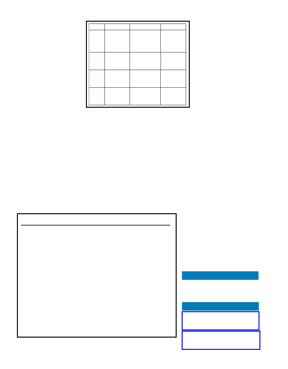
78
Issue 154 May 2003
CIRCUIT CELLAR
®
www.circuitcellar.com
used with a Gerber DS-274D
plot file, there wasn’t a vehicle
for carrying this information in
the plot file (unless you insert-
ed it into comment lines).
Note that the old vector
plotters used physical aper-
tures placed in a carrousel.
Therefore, you were limited
to whatever apertures the plot
house happened to own.
With the raster plotter,
apertures are virtual, and
they’re not limited to what
can be stocked. With RS274-X
came a myriad of aperture
possibilities. The descriptions
are now part of the plot file
and readable by the system.
This reduces the burden on you and
eliminates some nasty human trans-
lation errors.
Standard apertures include circle,
rectangle, oval, and polygon. These
are predefined and begin with a single
letter (see Figure 4). Custom apertures
are allowed (assuming they’re defined
first using the AM command) and
consist of multiple characters. The
aperture macro (AM) essentially
defines a single aperture made from
multiple primitives. Look at Table 3
for a short section of a Gerber file.
PHOTOPLOTTING
Regardless of the file’s format—
either RS274-D with a separate aper-
ture list or RS274-X with embedded
aperture—the Gerber files give the fab
house the information it needs to pro-
tect areas of copper on your PCB from
getting etched off. But wait—remem-
ber that before any copper is etched
off, holes must first be drilled. This is
because the plating process uses the
copper top and bottom for its electri-
cal path. The CAD output from your
PCB design is also responsible for out-
Table 3—
Although this file is an RS274-X extended data file, the actual data is in the RS274-D format. The X for-
mat allows all of the set-up parameters to be machine read. This reduces the possibility of human error.
Lines of actual Gerber file
RS-274-type and comments
G75*
D—Enable 360° circular interpolation
G70*
D—Inches
%OFA0B0*%
X—Offset file reference X/Y to plot reference A/B
%FSAX24Y24*%
X—Absolute values with two integers and four decimal places
%IPPOS*%
X—Positive image polarity
%LPD*%
X—Dark layer polarity
%AMOC8*
X—Aperture “OC8” macro eight-sided polygon with an outside width of
1.08239 times the value in the A/D command and rotated 22.5°
5,1,8,0,0,1.08239X$1,22.5*
*%
%ADD10C,0.0000*%
X—Aperture D10 a circle with a minimum diameter
…
%ADD16OC8,0.0520*%
X—Aperture D15 defined by the OC8 macro above
D10*
D—Use aperture D10
X042363Y024275D02*
D—Move to X = 4.2363, Y = 2.4275 with the light off
X002370Y024285D01*
D—Move to X = 0.2370, Y = 2.4285 with the light on
X002370Y001285D01*
D—Move to X = 0.2370, Y = 0.1285 with the light on
…
D16*
D—Use aperture D16
X019369Y018280D03*
D—Move to X = 1.9369, Y = 1.1280 with the light off, then flash the light
on and off
X023369Y018280D03*
D—Move to X = 2.3369, Y = 1.1280 with the light off, then flash the light
on and off
M02*
D—End of file
Jeff Bachiochi (pronounced BAH-key-
AH-key) has been writing for
Circuit
Cellar since 1988. His background
includes product design and manu-
facturing. He may be reached at
jeff.bachiochi@circuitcellar.com.
REFERENCE
[1] Steve DiBartolomeo,
Photoplotter sketches, Artwork
Conversion Software, Inc., 1991.
RESOURCES
ManiaBarco, Inc., Gerber file for-
mat (RS274-X), www.maniabar-
co.com.
Excellon Automation Co., “Part
Programming Commands,”
www.excellon.com.
putting files for the NC drilling
machines. As you can probably
guess, the process of drilling
holes is extremely close to that
of the photoplotter. So, you
won’t be surprised to find the
parallels between plot and drill
files. Take a look at the refer-
ences I’ve provided for more
information on the Excellon
drill format.
I hope that you’re as curious
as I am about the tools you
use. If you’re looking for a rea-
son to learn more about these
formats, let me suggest a way
you can save a few bucks,
especially if you get a lot of
designs prototyped.
Prototyping PCBs can easily cost
$100 for a couple of boards. The rea-
son is that there is usually a set-up
charge in addition to the cost per
square inch of material. For small
boards, this can be a major part of the
cost. By understanding the file for-
mats you can create files that con-
tain multiple boards within the
same file. These will be treated as a
single board and returned to you as
such. You will need to cut them
apart, but it’s worth the effort. One
caveat remains: both the Gerber and
NC drill files need to have the same
offsets for each artwork included.
Piece of cake, right?
I
Circle
Shape
Outside diameter
Required
(for round hole)
Inside diameter
or
(for rectangular hole)
x-axis dimension
y-axis dimension
Optional
%ADD10C,0.05
X0.01
X0.02*%
Command form
Rectangle x-axis dimension
y-axis dimension
x-axis hole dimension
y-axis hole dimension
%ADD11R,0.05
X0.08
X0.02
X0.04*%
Oval
x-axis dimension
y-axis dimension
x-axis hole dimension
y-axis hole dimension
%ADD12O,0.05
X0.08
X0.02
X0.04*%
Polygon
Outside dimension
Number of sides
Degrees of rotation
x-axis hole dimension
y-axis hole dimension
%ADD13P,0.05X6
X0
X0.02
X0.04*%
Figure 4—
Take a look at the standard predefined apertures for RS274-X.
Custom apertures can be designed using the aperture macro command (AM).
80
Issue 154 May 2003
CIRCUIT CELLAR
®
www.circuitcellar.com
eruse the local
bookstore or tune in
to one of the daytime
talk shows, and it won’t be
long before you come across something
in the War of the Roses or Mars-versus-
Venus vein. Heck, “Can’t live with ’em,
can’t live without ’em” has been a hot
topic ever since Adam and Eve.
If Oprah had earned an E.E. degree,
you might have seen an episode enti-
tled, “Analog vs. Digital: Can We All
Get Along?” In the old days, when
bits were bits and signals were signals,
things were conceptually, if not prac-
tically, simpler. There was a demilita-
rized zone fenced with A/D and D/A
converters, placing real-world signals
(and a lash-up of op-amps and dis-
cretes) on one side, and ones and zeros
(i.e., a processor) on the other.
You’d think the ability to cram
practically everything into a single
chip would make the issue go away.
After all, what MCU worth its salt
doesn’t have a built-in A/D converter
at this point? But it’s not that simple.
The good news is that there are more
and more unique chips to use as links
in the signal chain. But more choices
mean more head scratching to figure
out the optimal design.
Digilog Déjà Vu
p
Tom Cantrell
Tom’s
been
working
the ana-
log PLD
beat for us for several
years now. This latest
update comes on the
heels of his recent
investigation into
Anadigm—one of the
fresher faces to hit
the “digilog” scene.
SILICON
UPDATE
GENDER BENDER
This is the fourth time I’ve written
up the class of chips typically known
as analog PLDs. I’ve used the term
“digilog” to describe these analog and
digital combos. To my mind, much of
the original credit for the concept goes
to a little-known outfit, IMP, whose
EPAC chip I wrote up way back in
1995 (“EPAC Epoch,” Circuit Cellar 58).
Then, in 1997 I covered Motorola’s
nascent foray into the biz with their
Motorola programmable analog array,
a.k.a. MPAA (“A(r)Ray of Analog
Hope,” Circuit Cellar 87).
For a variety of reasons neither IMP
nor Motorola were able to make a go
of it. The question raised is whether
the concept of an analog PLD is funda-
mentally flawed, or whether it’s more
a matter of corporate mismatch and
distraction.
Lattice’s entrance into the market
with the PAC chip a while back is
surely an argument in the digilog con-
cept’s favor (“Analog PLD Anyone?”
Circuit Cellar Online
, March 2000).
Going through the datasheet at that
time, I couldn’t help noticing what
seemed to be a familial resemblance
to the original IMP parts. I suppose I
shouldn’t have been surprised when I
called Lattice to chat, and ended up
talking to the same IMP folks I had
talked to five years earlier!
Yes, it’s a small world after all.
Check out start-up Anadigm and their
latest Analog PLDs, and, underneath a
shiny new corporate logo and organi-
zation chart, you’ll find the Motorola
MPAA team and technology ramping
up for a second round.
HISTORY LESSON
Indeed, Anadigm will sell you an
AN10E40 chip and AnadigmDesigner
software that, although renamed, traces
Photo 1—
The $499 Vortex EV Kit makes it easy to eval-
uate Anadigm’s latest take on the analog PLD concept.
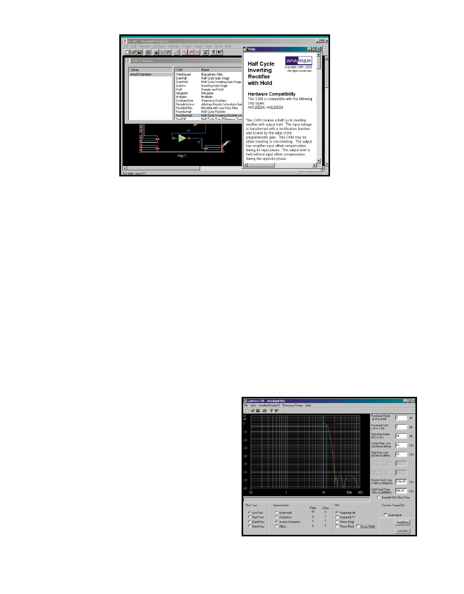
www.circuitcellar.com
CIRCUIT CELLAR
®
Issue 154 May 2003
81
the inputs through the
CABs to the outputs.
The CABs now have
two op-amps, eight pro-
grammable capacitor
arrays (twice the origi-
nal), and a comparator.
Brand new to Vortex, the
CABs also include an 8-
bit successive approxi-
mation register, or SAR
(i.e., A/D converter), as
well as a 256 × 8 look
up table (LUT) and a
programmable counter
(see Figure 2).
The SAR isn’t really
intended for the designer
to use directly as an 8-bit ADC, although
it’s possible to output a digital represen-
tation. Rather, it’s intended to enable
such functions as automatic gain con-
trol. More generally, it means the chip
can dynamically change its own config-
uration (e.g., gain, frequency, etc.) to
automatically adapt in real time.
The SAR can also work with the
LUT, providing a straightforward
mechanism for calibrating and “lin-
earizing” the output of a particular
sensor. Alternatively, drive the LUT
address inputs with the programmable
counter, and you’ve got an arbitrary
waveform generator.
Going a bit deeper, analog purists
should be pleased with the significant
improvement in the raw op-amp specs.
Overall bandwidth jumps up to 2 MHz,
which is almost 10 times better than
its roots right back to the
technology that I covered
five years ago. If you refer
to my original article,
you’ll see that even
though I was (and remain)
open to the digilog con-
cept, I raised a few real-
world concerns about the
specific MPAA20-now-
AN10E40 implementa-
tion. As with all chips,
these boiled down to
issues related to cost, per-
formance, and ease-of-use.
It’s no secret that Xilinx
and Altera make tons of
money with their high-end
digital FPGAs, and I’m talking about
chips with price tags up to $1000 and
beyond. Thus, I suppose it must have
seemed reasonable at the time for the
MPAA20-now-AN10E40 to come out of
the chute with a rather luxurious piece
of silicon. But, as I wrote in that original
article, in terms of driving the market,
“Motorola’s $50 price tag for the MPAA
doesn’t exactly prod things along.”
Traditional analog design can border
on black magic, and accomplished sor-
cerers are a fussy breed. Yeah, they’ll sit
through your pitch on analog PLDs, digi-
tal signal processing, and all the rest, but
just be prepared to answer some tough
questions about bandwidth, signal-to-
noise ratios, and so on. Low-performance
pretenders need not apply, and the origi-
nal MPAA specs were a bit iffy. Probably
the most showstopping of them was
the single-ended architecture, simply a
no-no for high-fidelity apps where the
common-mode noise-immune differ-
ential architecture is a must.
The original version of the software
tool—EasyAnalog—partially lived up
to its name with macros to imple-
ment higher-level functions such as
filters. Nevertheless, under the veneer
it was largely a structural tool, tempt-
ing if not compelling designers to run
wires from one op-amp to another.
This might appeal to the most experi-
enced and capable analog designers,
but it wasn’t conceptually any easier
than the old ways.
As it remains today, the original
part’s SRAM-based configuration
made for pretty quick blow-and-go
evaluation. Yes, you could wire up the
chip and start probing with a scope,
but, nevertheless, I noted that a simu-
lator would have been helpful for
exploring the device’s capabilities.
With this background, it’s time to
take a look at what’s new from
Anadigm now that they’ve cut the
apron strings from Motorola. I think
you’ll find they’re getting past the grow-
ing pains with new chips that address
the earlier concerns and ultimately fur-
ther the cause of the digilog concept.
LESS SHOW MORE GO
Enough of the background—let’s get
right under the hood of the new
AN120E40 and ’220E40 Vortex parts
(see Photo 1). Just as digital program-
mable logic chips rely on configurable
logic blocks, the Anadigm chips incor-
porate a quartet of
configurable analog
blocks, or CABs (see
Figure 1). This is far
less than the 20 CABs
found on the original
part, and note also
that the package has
downsized to a practi-
cal 44 pins.
Although reduced in
quantity, the underly-
ing functionality of
the CABs and I/O has
been significantly
improved. The most
notable upgrade was
the adoption of a fully
differential path from
Photo 2—
High-level configurable analog modules hide the complexity of the underlying hardware.
Photo 3—
With AnalogDesigner2, sophisticated filter design is a point-and-click
affair. Also new is the ability to automatically partition complex designs across
multiple chips—as is the case here for a Butterworth filter.
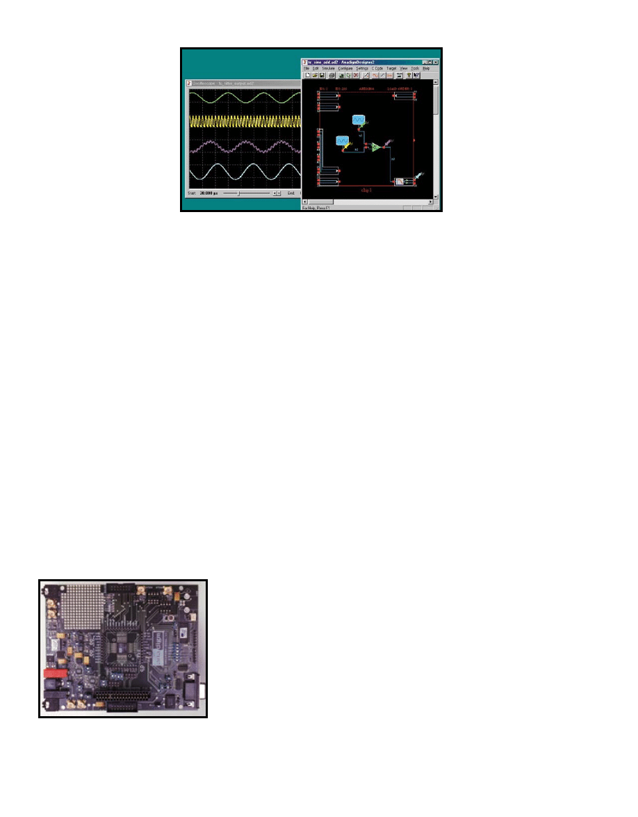
82
Issue 154 May 2003
CIRCUIT CELLAR
®
www.circuitcellar.com
tion that would, for exam-
ple, reprogram the boot
EEPROM from time-to-
time via a temporary con-
nection to a PC.
The real-time dynamic
reconfigurability of the
’220 is accomplished by the
addition of a shadow RAM
that duplicates the primary
configuration RAM. This
allows you to initialize the
shadow RAM in the back-
ground and, after it’s
loaded, perform reconfigu-
ration in a single clock
cycle. The quick switch-
over allows the part to maintain con-
tinuous operation across the reconfigu-
ration without the delays and
headaches of a more traditional (and
slow) stop everything and reload ritual.
There are four ways to trigger the
reconfiguration (i.e., the transfer from
shadow RAM to configuration RAM)—
one manual and three automatic. As for
the former, the Execute pin enables an
MCU or other external digital logic to
initiate the transfer.
As I mentioned earlier, automatic
reconfiguration gives the part its unique
ability to dynamically adjust its own
behavior, up to and including the analog
equivalent of self-modifying code. Here’s
how it works. The output of the SAR-
ADC, used either directly or to address
the LUT, can be routed back into its
host CAB. Actually, it’s a two-step,
semicircular process. The output of the
SAR-ADC (or the corresponding LUT
entry) is specified to write to one or two
byte locations in the shadow RAM.
After writing the final byte, an automat-
ic transfer is triggered, thus updating the
configuration RAM with the recently
modified contents of the shadow RAM.
A reconfiguration also can be trig-
gered directly by the state of an analog
signal, either based on a zero crossing
or comparator output. This allows
glitch-free timing of the reconfigura-
tion to minimize the disruption to
ongoing analog processing.
SIM CITY
The latest-generation software tool—
AnadigmDesigner2—is more than just a
new and improved tweak of the original
the original. Similarly, new
input circuitry cuts DC off-
set from 10 mV of the origi-
nal to just 100 µV—welcome
relief when working with
low-output sensors and high
gain settings. Thanks in large
part to the differential archi-
tecture, other specs (e.g.,
SNR, output slew rate, cross-
talk rejection, etc.) are signif-
icantly improved, as well.
Concerning I/O, the chip
incorporates four analog input
cells, one of which is fronted
with a 4:1 multiplexing option
and two analog output cells.
The differential signal path is carried all
the way from input to output pins, sup-
porting larger designs that partition
the required functionality across mul-
tiple chips. Single-ended connections
are accommodated via a built-in level
shifting between virtual and physical
ground references.
Input cells incorporate eight-level
programmable gain amps (powers of
two from 0 to 7—that is, 1 to 128),
eliminating the need to devote a CAB to
the purpose. All cells (input and output)
include an optional low-pass filter with
an adjustable corner frequency from
8 to 470 kHz to handle basic input
antialiasing and output smoothing, once
again preserving CABs for real work.
Behind the scene (i.e., CABs and I/O
cells), the chip includes the glue logic
needed to get the job done, including
various reference voltages and non-
overlapping clocks that put the
“switch” in switched capacitor.
GO CONFIGURE
Now is a good time to point out
that the only difference between the
’120E40 and ’220E40 relates to config-
uration. Specifically, the ’120 is
intended to be configured only once at
power-up, while the ’220 can be not
only dynamically reconfigured, but
indeed designed to exploit reconfigura-
tion in the normal course of operation.
Although it requires more than a
few pins and the close reading of the
datasheet, give Anadigm credit for craft-
ing a flexible scheme. Configuration
options include standard serial
EEPROMs, FPGA-oriented EEPROMs,
and a generic clocked serial interface
for easy connection to any MCU.
There’s also a daisy-chain mecha-
nism to initialize multiple chips and
synchronize their operation.
You should carefully consider
whether or not you truly need, or
even desire, the ’220’s dynamic recon-
figuration capability for your applica-
tion. Although both are much less
expensive than the original Motorola
part, the ’220’s price is notably higher
than the ’120’s—$15 versus $7.95
(10,000 quantity), respectively.
For relatively infrequent changes,
such as calibration (and recalibration),
it’s simple enough to craft a system
using a low-cost flash memory MCU
storing multiple configurations. Beyond
a bit of protocol overhead, a particular
configuration consumes only 576 bytes:
64 bytes for each CAB (i.e., 64 × 4), 64
for the overall chip configuration, and
256 for the LUT. Alternatively, you
could design an EEPROM-based solu-
Photo 4—
The simulator—with its friendly oscilloscope-like interface—is a welcome
addition to AnadigmDesigner2. This run shows how the built-in output cell filter pass-
es only the low-frequency component of a mixed low- and high-frequency sine wave.
Photo 5—
The evaluation kit interfaces to a PC COM
port via an on-board MCU, and sockets for boot
EEPROMs (both standard and FPGA-type) are also
provided. In addition, daughtercards with additional
AN220E40s can be added to prototype multichip designs.
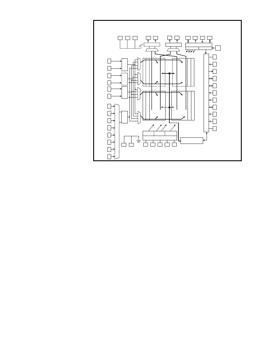
www.circuitcellar.com
CIRCUIT CELLAR
®
Issue 154 May 2003
83
version. There are some fundamental
enhancements that I’ll describe, but
also what I would characterize as a
change in philosophy.
You’ll recall that one of my misgiv-
ings about the first-generation soft-
ware was the feeling that it’s structur-
al facade made it a bit daunting, leav-
ing too little of the silicon underpin-
nings to the imagination. Review the
screen shots from that earlier article
and you’ll see what looks more like a
die photo than a schematic. Yes, there
were macros and a pretty GUI, but I
just couldn’t shake the impression that
you still had to be something of an
analog guru to get the most out of it.
By contrast, AD2 has a higher-level
feel. The macro (called CAM for con-
figurable analog module), not the
CAB, is the basic design element. You
simply cut and paste relatively high-
level functions with little concern for
the underlying details (see Photo 2).
My only complaint is that as you
add CAMs, the tool doesn’t give you
any feedback on how many resources
have been consumed or remain avail-
able. You simply know that you’ve hit
the limit when AD2 refuses to let you
insert another CAM. However, when
I mentioned this to the folks at
Anadigm, I was informed that a
resource meter will be added in the
next release of AD2, which should be
out by the time you read this article.
Going beyond CAMs, AD2 extends
beyond structure into the realm of
behavioral definition. Consider the fil-
ter design capability demonstrated in
Photo 3. You simply point, click, and
drag your desired filter specs (i.e.,
type, frequency, attenuation, etc.), and
the proper CAMs are dropped into the
chip, or indeed chips.
And this time around, the software
includes a simulator, which is a wel-
come addition. I found it to be friendly
and easy to use, especially the virtual
signal generators and virtual oscillo-
scope (see Photo 4). Even though simu-
lations actually take longer than down-
loading the configuration, we’re talking
only a few seconds in either case, and
I enjoyed the WYSIWIG reassurance.
Thanks to ease of use and the new
features, I think AD2 actually moves
beyond the realm of useful into educa-
tional and even fun. In fact, even engi-
neers who don’t have an imminent
application might consider checking
out the kit or the even the free evalua-
tion copy of the software (see Photo 5).
AD2 is a quick and easy way to learn
about, experiment with, and evaluate
the digilog concept.
C BREEZE
Another first for AD2 is the inclu-
sion of automatic C driver code gener-
ation that exploits the dynamic recon-
figuration capability of the chip. Once
again, this represents a step up the
ladder toward a higher-level, simpler,
and easier-to-understand way of deal-
ing with the underlying hardware. For
instance, instead of hacking a configu-
ration RAM bit map directly (e.g.,
poking in what you hope to be proper
changes for the capacitor arrays or
wiring), AD2 creates a simple API
with functions like Set Gain or Set
Corner Frequency.
Each CAM in the AD2 library comes
with a set of related drivers. To econo-
mize, you’re allowed to turn off driver
generation for CAMs that are never
reconfigured. Furthermore, by virtue
of a CAM ID scheme, only a single
instance of a driver is needed to manip-
ulate multiple CAMs of the same type.
In addition to CAM-specific drivers,
AD2 also generates routines that man-
age various aspects of overall chip oper-
ation. For instance, drivers that control
the on-chip clock generator provide the
basis for a low-power Sleep mode.
Without having fully evaluated the
C driver feature, I have to admit some
concerns related to code bloat, and
possible C portability and compatibili-
ty issues. Nevertheless, it’s conceptu-
ally a great approach and almost cer-
tainly better in practice than the alter-
native of leaving you to deal with all
the gory details from scratch.
SHIFTING SANDS OF SILICON
The downsized form factor (and
price) of the new chips is welcome, as
are the improved fidelity and band-
width. And the unique dynamic self-
reconfiguration capability of the
’220E40 certainly stands out and should
AV
D
D
AV
D
D
2
SHIELD
Output cell 2
O2P
O2N
Output cell 1
O1P
O1N
A
CLK
OUTCLK
DCLK
DOUTCLK
Oscillator and clocks
Analog
Logic
Mode
1 2 3 4
Input
cell 1
I1P
I1N
Input
cell 2
Input
cell 3
A
B
C
D
I2P
I2N
I3P
I3N
I4PA
I4NA
I4PB
I4NB
I4PC
I4NC
I4PD
I4ND
Input
cell 4
A
VSS
SVSS
Shado
w RAM
Configur
ation RAM
CAB1
CAB2
Configur
ation RAM
Shado
w RAM
Shado
w RAM
Configur
ation RAM
CAB3
CAB4
Configur
ation RAM
Shado
w RAM
BVDD
VREFPC
VMRC
VREFNC
BVSS
Voltage references
V
REF+
V
REF–
VMR
Look-up table
DVDD
DIN
2
LCCb
ERRb
1, 3
ACTIVATE
1, 2
EXECUTE
PORb
CFGFLGb
1, 2
Configur
ation interf
ace
CS1b
CS2b
DVSS
1
Open drain output
2
Programmable internal pull-up
3
10-k
Ω
External pull-up recommended
Figure 1—
The analog corollary to an FPGA, the AN120/220E40 connects configurable analog blocks (CABs) with
a programmable interconnect and I/O cells.
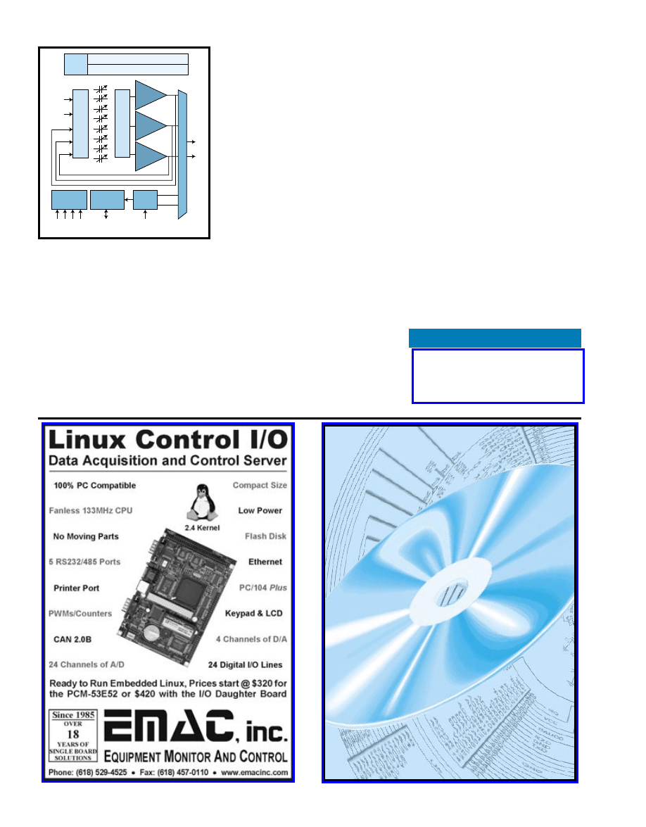
84
Issue 154 May 2003
CIRCUIT CELLAR
®
www.circuitcellar.com
inspire designer creativity. Finally, the
new tools and their friendlier face help
a lot to further the digilog concept.
I think the concept is a winner, but
the rate of success likely depends as
much on how it is sold and to whom as
the technology itself. When the concept
first appeared, it was only natural that
the audience tended to be experienced
analog designers. In turn, that put the
focus on the issues of raw analog per-
formance and component cost (i.e., ver-
sus op-amps). You don’t have to be an
analog expert to see that Vortex repre-
sents a big improvement in these areas.
And, thanks largely to the new features
and philosophy of the AD2 tool suite,
Vortex and the digilog concept are
accessible to any designer, not just op-
amp uber alles gurus.
The caveat is that the silicon world
never stands still, and the current
technology and competitive battle-
ground looks significantly different
than it did five years ago. Witness the
emergence and widespread adoption
of low-cost DSP technology in the
form of flash memory-based DSP
Controllers, not to mention the MAC
instructions and ever-higher resolution
A/D converters in your favorite MCU.
Or, what about digital sensors that
bury the signal conditioning inside?
Devices like a Dallas digital tempera-
ture sensor, TAOS photodetector, or
Analog Devices accelerometer put out
Tom Cantrell has been working on
chip, board, and systems design and
marketing for several years. You may
reach him by e-mail at tom.cantrell@
circuitcellar.com.
SOURCE
AnadigmDesigner2 software,
Vortex FPAA family
Anadigm, Inc.
www.anadigm.com
ones and zeros, so there’s no need for
op-amps, filters, A/Ds, or anything else.
Over the years, with the march of
silicon, engineering has continued to
evolve from “how to” to “Which is
the best way?” Designers need to get
the big picture of their designs all the
way from one side of the PCB to the
other, taking a holistic and strategic,
not just tactical chip-by-chip, view.
The good news is that the prolifera-
tion of technologies means engineer-
ing remains interesting work, not to
mention further insuring there’s some
work to be had. Don’t you just love
this business?
I
Shadow SRAM
Configuration SRAM
Control
logic
Switch matr
ix
Global
Local
Switch matr
ix
Op-amp
Comp
Op-amp
NOL clock
generator
LUT
interface
SAR
logic
Data
Sync
1 2 3 4
Analog clocks
Look-up
table
SAR
clock
V+
V–
Figure 2—
Each CAB is built around a pair of op-amps
and a comparator. New to Vortex CABs are a fully dif-
ferential architecture, successive approximation register
(SAR) A/D converter, and Shadow RAM.
w..cciirrccuuiittcceellllaarr..ccoom
Go to our web
site to get all of
the Circuit Cellar
back issues on
CD-ROM.
www.circuitcellar.com
CIRCUIT CELLAR
®
Issue 154 May 2003
85
IDEA BOX
THE
DIRECTORY
OF
PRODUCTS AND
SERVICES
AD FORMAT
: Advertisers must furnish digital submission sheet and digital files that meet the specifications on the digital submission sheet.
ALL TEXT AND OTHER ELEMENTS MUST FIT WITHIN A 2
″″ ××
3
″″
FORMAT
. Call for current rate and deadline information. Send your disk and digital submis-
sion sheet to: IDEA BOX, Circuit Cellar, 4 Park Street, Vernon, CT 06066 or e-mail kc@circuitcellar.com. For more information call Sean Donnelly at (860) 872-3064.
Suppliers Directory now available online. Check out our web site
www.circuitcellar.com to see who has what and how to get it!
Ready-Made Graphical User Interface
Bright, High Contrast 1/4 VGA (320x240 pixel)
Electroluminescent (EL) or Monochrome Display
Precoded menu managing software
Real-time Multitasking Executive
tel: 510-790-1255 fax: 510-790-0925
applications - wherever you need an I/O rich computer and
Insert-ready Single Board Computer modules in sub-miniature
dimensions (as small as 47x55 mm) populated by:
applicable controller signals extend to standard pin header (2.54
mm) or high-density Molex (0.625 mm) connectors, enabling SBC
to be plugged like a big chip into OEM targets
achieved via GND circuitry, multi-layer PCB, by-
pass capacitor grid and short signal traces achieved via small
footprint and use of 0402 SMD passive components
32 KB to 64 MB external SRAM and Flash (controller-dependent)
CAN, Ethernet, RS-232 and RS-485 interfaces; ADC, DAC
(controller-dependent); freely-available /CS and I/O lines
AC adapter, serial cable and SPECTRUM CD with eval software
tools, electronic documentation and demos
: insert-ready PHYTEC SBC modules accompany you
from evaluation through protyping to end production...
accelerating your design cycle and reducing your time-to-market
86
Issue 154 May 2003
CIRCUIT CELLAR
®
www.circuitcellar.com
Interface Keypads, Switches, or RS-232 to your PC Keyboard Input
Up to 12 x 12 matrix Programmable RS-232 Port Macro Capability
The KE24 is the ultimate in flexibility. Inputs or serial data can
emulate any of the 101 keys from a standard keyboard.
Up to 9 x 9 matrix 2.5" x 3.0" Size PC Keyboard Port PCXT, AT Compatible
The KE18 combines a multitude of features with small size at an
economical price. Custom units available.
Phone: 607-533-4441 Fax: 607-533-4443
Decade Engineering
503-743-3194
Turner, OR, USA
Call 530-297- 6073 Email sales
www.circuitcellar.com
CIRCUIT CELLAR
®
Issue 154 May 2003
87
Now get ISO-9002 Quality PCB Prototypes for the best Prices

88
Issue 154 May 2003
CIRCUIT CELLAR
®
www.circuitcellar.com
sales@sealevel.com 864.843.4343
1,2,4, and 8-port mode
RS-232, RS-422/485, a
6 models offer TTL input/output,
www.circuitcellar.com
CIRCUIT CELLAR
®
Issue 154 May 2003
89

90
Issue 154 May 2003
CIRCUIT CELLAR
®
www.circuitcellar.com

www.circuitcellar.com
CIRCUIT CELLAR
®
Issue 154 May 2003
91

92
Issue 154 May 2003
CIRCUIT CELLAR
®
www.circuitcellar.com

www.circuitcellar.com
CIRCUIT CELLAR
®
Issue 154 May 2003
93

Build a Graphical User Interface with TcI/Tk
Time-Triggered Technology
Construct a Hand-Held Radiation Monitor
Short Solution: The Perfect PCB Prototype
Mad Dash for Cash Microchip Design Contest 2002 Winners
IaRobotics Corner: The Altmotor
IaAbove the Ground Plane: Battery Power—Feeding the Z3801A
I Applied PCs: Build a Coyote Protocol Converter
I From the Bench: Encore!—Zilog’s Z8 Flash Memory-Based Micro
I Silicon Update: Good Vibrations
Preview of June Issue 155
Theme: Measurement & Sensors
94
Issue 154 May 2003
CIRCUIT CELLAR
®
www.circuitcellar.com
INDEX
91
Abacom Technologies
56
Accutech
86
ActiveWire, Inc.
35
All Electronics Corp.
90
Amazon Electronics
93
AP Circuits
7
Atmel
93
Avocet Systems, Inc.
91
Bagotronix, Inc.
31
Basic Micro
91
Bellin Dynamic Systems, Inc.
47
CadSoft Computer, Inc.
89
Carl’s Electronics
16
CCS-Custom Computer Services
39
Cogent Computer Systems, Inc.
92
Conitec
11
Connecticut mircoComputer, Inc.
85
Cyberpak Co.
1
Cypress MicroSystems
90
CWAV
16
Datadog Systems
91
DataRescue
86
Decade Engineering
88
Delcom Engineering
58
DesignCon East
48
Earth Computer Technologies
The Advertiser’s Index with links to their web sites is located at www.circuitcellar.com under the current issue.
Page
87
EE Tools
(Electronic Engineering Tools)
84
EMAC, Inc.
90
Embedded Micro Software
91
EmbeddedPCI.com
90
eProtos.com
9
ExpressPCB
86
FDI-Future Designs, Inc.
92
Front Panel Express
86
Hagstrom Electronics
49
HI-TECH Software, LLC
92
HVW Technologies Inc.
66
ICOP Technology Inc.
89
IMAGEcraft
89,93
Intec Automation, Inc
86
Intrepid Control Systems
91
Intronics, Inc.
30
Intuitive Circuits, LLC
17
Jameco
64, 86
JK microsystems, Inc.
30
JR Kerr Automation & Engineering
30
LabJack Corp.
77
Lakeview Research
73
Lemos International
2
Link Instruments
69
Linx Technologies
42
MaxStream
90
MCC (Micro Computer Control)
67
Microchip
92
microEngineering Labs, Inc.
79
Micromint
85
Mosaic Industries, Inc.
33
Motorola
15
Motorola Contest
90
Mouser Electronics,Inc.
50
MVS
86
Mylydia Inc.
C2
NetBurner
88
OKW Electronics, Inc.
67
On Time
92
Ontrak Control Systems
56
PCBexpress
87
PCB Fab Express
9
PCBpro
C4
Parallax, Inc.
85
Phytec America LLC
87
Phyton, Inc.
93
Picofab Inc.
89
Pioneer Hill Software
16
Polydroids
77
Prairie Digital, Inc.
85
QKITS.COM
88
R2 Controls
Page
Page
Page
ADVERTISER’S
57
R4 Systems Inc.
65
Rabbit Semiconductor
73
Remote Processing
90
RLC Enterprises, Inc.
5
Saelig Company
3
Scott Edwards Electronics Inc.
88
Sealevel Systems
87
Senix Corp.
18
Sensors Expo & Conference
95
Sierra Proto Express
85
Signum Systems
93
Softools
93
Spectrum Engineering
85
Square 1 Electronics
88
TAL Technologies
C3
Tech Tools
40,41
Technologic Systems
89
Technological Arts
89
Tern Inc.
91
Triangle Research Int’l, Inc.
11
Trilogy Design
93
Weeder Technologies
93
Xeltek
87
Z-World
88
Zanthic Technologies Inc.
23
Zilog, Inc
July Issue 156
Deadlines
Space Close: May 9
Material Due Date:
May 20
Theme:
Embedded Programming
A
TTENTION
A
DVERTISERS
Call Sean Donnelly to
reserve your space!
860.872.3064
e-mail: sean@circuitcellar.com
For Unparalleled
Quality, Technology,
Delivery and Price
Insist on 2 to 24 layer
PCBs from Sierra Proto
Express
q
u
a l
i t y l e a d
e
r
M
IL
-P-5
5110 ISO
90
0
2
•
40
8-
73
5-7
137
www.protoex
pre
ss
.c
om
•
We offer the highest quality, the broadest range of technology (2 – 24 layers), the fastest, most
reliable turns (99% on-time delivery) and a competitive price. And we prove it every day,
with every PCB we ship.
With every multilayer order you receive "Evidence of Quality" which is a
set of 5 reports. Microsection Analysis, such as the one featured here, is
one of those reports, which provides a proof that your board meets or
exceeds your specifications.
Order from us, benchmark our quality, technology, delivery and service
with whoever you are currently doing business with, send us that report
and
receive our special T-Shirt commemorating our 17th year of success.
Mention promotion code: PCCB00043.
For proven quality that never costs extra,
put Sierra Proto Express
on your team today.
Call our expert Technical Advisors at
408 735 7137
or visit us at
Microsection
14 Layer Board
s I write this I’m sitting in the waiting room at a car dealership. I’m not in the part of the dealership that sells the cars. They
already pulled that trick. This is where they have you wait when the car fails the end-user application. I’m in the BMW Service
Department waiting room. As you might guess, I’m not alone. There are four other men and three women who look agitated either at hav-
ing to be late for work because their cars broke down or because they’re the ones stuck doing the dirty work for their spouses. These days,
BMW ownership isn’t gender-specific. Failure is now an equal-opportunity frustration.
A full waiting area always elicits predictable behavior. Invariably, people start describing their car problems almost in a game of one-upmanship. One guy looked
up from his newspaper and said, “I got into the car yesterday and turned the lights on. Instead of the lights, the left rear window went down and the radio went on!”
You think that’s bad, another guy added, “I was on the entrance ramp and stomped on the gas. All of a sudden everything turns to crap. The engine drops
to 500 rpm, and I get a stupid message that says Engine Failsafe Program–Service Engine Soon. You can say that again!”
A large elderly lady in the corner of the waiting room shouted, “Heck, that’s nothing. Every time I put the key in the ignition, the front seat looses its marbles
and goes back to the factory default for some emaciated assembly mechanic. If I don’t hit the seat-position stop button quickly, I’m in a $75,000 trash com-
pactor.” And so it continues around the room.
In deference to automobile and electronics manufacturers everywhere, I have to qualify my biased opinions by telling you that I have a zero-tolerance policy
for electronic things that don’t work right. With many of them I have an ultimate remedy. If I get truly frustrated, I just toss the thing in the trash and start again.
Yes, I realize this sounds like I’m ignoring remedial relief from manufacturers or retailers, but I factor that into my decision. Sometimes I just want the problem
to go away. It’s not about the lost value. It’s just…get this thing out of my face.
Unfortunately, cars are a bit of a different story. Although some people have those resources, I can’t just toss a car in the trash because it irritates me.
When it doesn’t work right I have to join the others in the Service Department waiting room and kill time until it’s my turn in the story-telling ring. Now that it’s
my turn, I say, “I’m sitting at my desk and all of a sudden I hear a car alarm system go off outside the building. I hear false alarms outside everyday from the
courthouse parking lot next door so it was nothing new. I was ready to ignore this one until I got a call from downstairs telling me it was my car this time. By the
time I got to the car, it stopped! It happened twice more in the next week.”
My story isn’t quite as thrilling as the guy who complained about the battery short that almost served up one of his passengers medium-rare (the battery is
under the rear passenger seat). Nevertheless, I continued, “If the alarm going off wasn’t bad enough, yesterday I come out to my car and not only is it
unlocked, all the windows are completely down and the sun roof is wide open. Talk about inviting problems!”
So, that’s the reason I’m sitting here—electronic gremlins! Alarms going off and windows opening. Unfortunately, publishing an embedded-control design
magazine doesn’t help, I assure you. It only reminds me that I have the inside track on knowing that total system meltdown is often only one watchdog timer
routine away. The more electronics we add to cars, appliances, and toasters, the more dependent we are on how they’re designed. It’s not about how great
they work when they run. It’s about how badly they perform when the operating code takes a left turn instead of a return.
I was going to relate more waiting room stories but my “personal service advisor” just told me the car is ready. He tells me, “Well, the computer registered the
alarms going off and indicated they were related to the hood switch. The plunger on your hood switch is too short, so we installed a plunger switch with a longer
plunger. As for the car opening by itself and the windows going down, how far is your office from where you park the car and is the key in your pocket?”
I was still mulling over the plunger deal as he talked. Bad hood switch? They’ve been making this car model for three and a half years. How did I get one
with a short plunger? Well, hopefully it’s fixed. And, oh yeah, “My office is about 100 feet from the car.”
Without the slightest expression of “you idiot,” my advisor continues, “Well, if you press and hold the key, it automatically lowers all the windows. This is a
program feature with the car. Just for you, however, we reprogrammed your key not to allow this function anymore. Just in case you sit on your key again.”
I’m not sure I totally buy this “operator error” explanation. It’s certainly not a big attention grabber among the waiting room crowd when it comes time to tell
your story, but I suppose it’s plausible. In truth, I’m not sure whether or not I’m more upset that the key might intermittently possess a range that allows me to
accidentally unlock the car. The other alternative is that this is all a crock of you-know-what, and I still have electronic gremlins. It would be a lot easier if I
could just throw it away and try another car.
Electronic Gremlins
INTERRUPT
a
steve.ciarcia@circuitcellar.com
96
Issue 154 May 2003
CIRCUIT CELLAR
®
www.circuitcellar.com
PRIORITY

Wyszukiwarka
Podobne podstrony:
circuit cellar2001 05
circuit cellar1997 05
circuit cellar2000 05
circuit cellar2002 05
circuit cellar1994 05
circuit cellar1993 05
circuit cellar2004 05
circuit cellar2003 05
circuit cellar1995 05
circuit cellar1996 05
circuit cellar2001 05
circuit cellar1997 05
circuit cellar1993 05
circuit cellar1996 05
circuit cellar2001 05
circuit cellar1995 05
circuit cellar1994 05
więcej podobnych podstron
