HCC/HCF4555B
HCC/HCF4556B
DUAL BINARY TO 1 OF 4 DECODER/DEMULTIPLEXERS
DESCRIPTION
.
EXPANDABLE WITH MULTIPLE PACKAGES
.
STANDARD, SYMMETRICAL OUTPUT CHAR-
ACTERISTICS
.
QUIESCENT CURRENT SPECIFIED TO 20V
FOR HCC DEVICE
.
5V, 10V, AND 15V PARAMETRIC RATINGS
.
INPUT CURRENT OF 100nA AT 18V AND 25
°
C
FOR HCC DEVICE
.
100% TESTED FOR QUIESCENT CURRENT
.
MEETS ALL REQUIREMENTS OF JEDEC TEN-
TATIVE STANDARD N
o
. 13A, ”STANDARD
SPECIFICATIONS FOR DESCRIPTION OF ”B”
SERIES CMOS DEVICES”
June 1989
The HCC4555B, HCC4556B (extended tempera-
ture range) and the HCF4555B, HCF4556B (inter-
mediate
temperature
range)
are
monolithic
integrated circuits available in 16-lead dual in-line
plastic or ceramic package and plastic micropack-
age.
The HCC/HCF4555B and HCC/HCF4556B are
dual one-of-four decoders/demultiplexers. Each
decoder has two select inputs (A and B), an Enable
input (E), and four mutually exclusive outputs. On
the HCC/HCF4555B the outputs are high on select ;
on the HCC/HCF4556B the outputs are low on se-
lect. When the Enable input is high, the outputs of
the HCC/HCF4555B remain low and the outputs of
the HCC/HCF4556B remain high regardless of the
state of the select inputs A and B.
EY
(Plastic Package)
F
(Ceramic Frit Seal Package)
M1
(Micro Package)
ORDER CODES :
HCC45XXBF
HCF45XXBM1
HCF45XXBEY
HCF45XXBC1
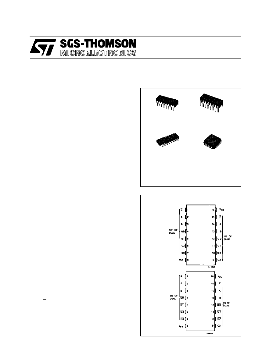
PIN CONNECTIONS
4555B OUTPUTS HIGH ON SELECT
4556B OUTPUTS LOW ON SELECT
4555B
4556B
C1
(Plastic Chip Carrier)
1/14
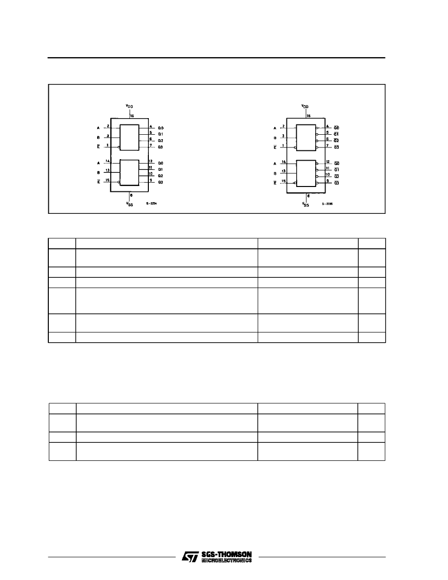
FUNCTIONAL DIAGRAMS
ABSOLUTE MAXIMUM RATINGS
Symbol
Parameter
Value
Unit
V
DD
*
Supply Voltage : HC C Types
H C F Types
– 0.5 to + 20
– 0.5 to + 18
V
V
V
i
Input Voltage
– 0.5 to V
DD
+ 0.5
V
I
I
DC Input Current (any one input)
±
10
mA
P
t o t
Total Power Dissipation (per package)
Dissipation per Output Transistor
for T
o p
= Full Package-temperature Range
200
100
mW
mW
T
o p
Operating Temperature : HCC Types
H CF Types
– 55 to + 125
– 40 to + 85
°
C
°
C
T
s t g
Storage Temperature
– 65 to + 150
°
C
RECOMMENDED OPERATING CONDITIONS
Symbol
Parameter
Value
Unit
V
DD
Supply Voltage : HCC Types
HC F Types
3 to 18
3 to 15
V
V
V
I
Input Voltage
0 to V
DD
V
T
o p
Operating Temperature : HCC Types
H CF Types
– 55 to + 125
– 40 to + 85
°
C
°
C
4555B
4556B
Stresses above those listed under ”Absolute Maximum Ratings” may cause permanent damage to the device. This is a stress
rating only and functional operation of the device at these or any other conditions above those indicated in the operational sec-
tions of this specifi cation is not implied. Exposure to absolute maximum rating conditions for external periods may affect device
reliability.
*
All voltages values are referred to V
SS
pin voltage.
HCC/HCF4555B/4556B
2/14
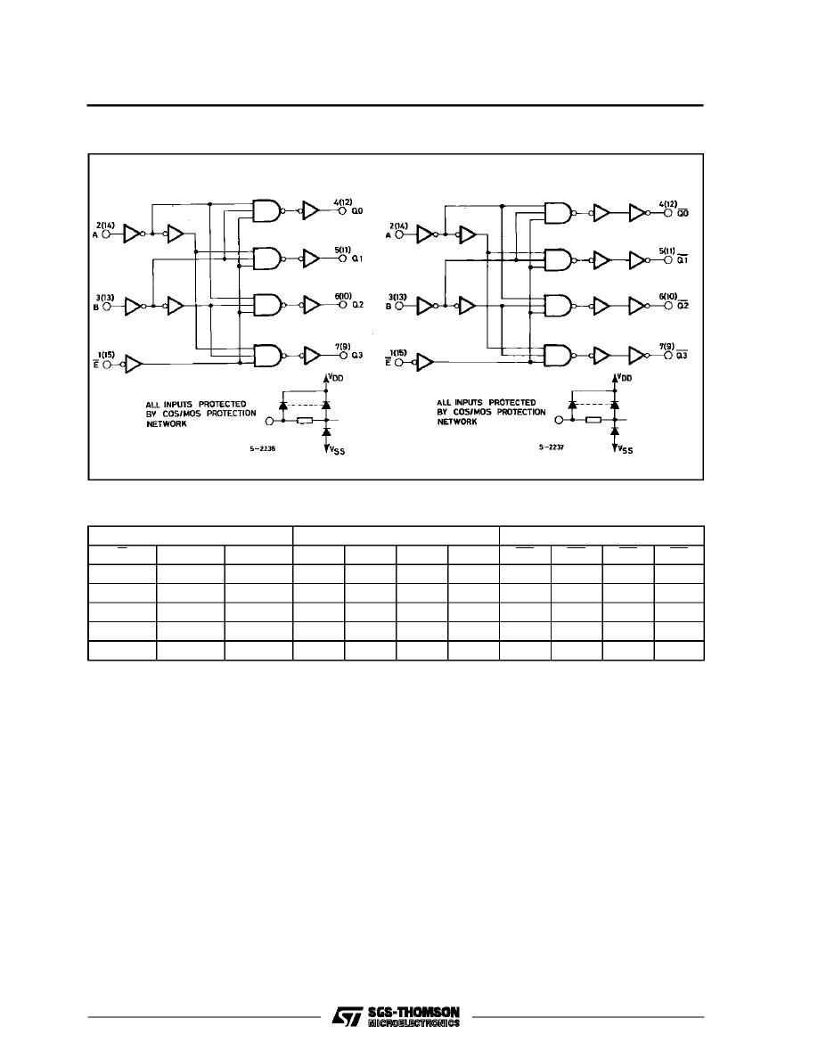
LOGIC DIAGRAMS
4555B
4556B
TRUTH TABLE
Inputs Enabl e Sel ect
Outputs 4555B
Outputs 455 6B
E
B
A
Q 3
Q 2
Q 1
Q 0
Q 3
Q 2
Q 1
Q 0
0
0
0
0
0
0
1
1
1
1
0
0
0
1
0
0
1
0
1
1
0
1
0
1
0
0
1
0
0
1
0
1
1
0
1
1
1
0
0
0
0
1
1
1
1
X
X
0
0
0
0
1
1
1
1
X = DON’T CARE, LOGIC 1 = HIGH, LOGIC 0 = LOW.
HCC/HCF4555B/4556B
3/14
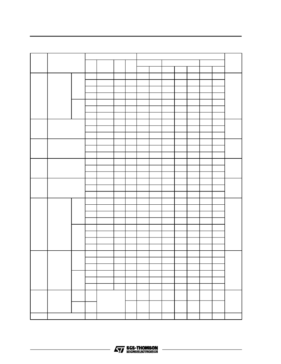
STATIC ELECTRICAL CHARACTERISTICS (over recommended operating conditions)
Test Conditions
Value
V
I
V
O
|I
O
|
V
D D
T
L o w
*
25
°
C
T
Hi g h
*
Symbol
Parameter
(V)
(V)
(
µ
A)
(V)
Min. Max. Min. Typ. Max. Min. Max.
Unit
I
L
Quiescent
Current
HCC
Types
0/ 5
5
5
0.04
5
150
µ
A
0/10
10
10
0.04
10
300
0/15
15
20
0.04
20
600
0/20
20
100
0.08
100
3000
HCF
Types
0/ 5
5
20
0.04
20
150
0/10
10
40
0.04
40
300
0/15
15
80
0.04
80
600
V
O H
Output High
Voltage
0/ 5
< 1
5
4.95
4.95
4.95
V
0/10
< 1
10
9.95
9.95
9.95
0/15
< 1
15
14.95
14.95
14.95
V
O L
Output Low
Voltage
5/0
< 1
5
0.05
0.05
0.05
V
10/0
< 1
10
0.05
0.05
0.05
15/0
< 1
15
0.05
0.05
0.05
V
IH
Input High
Voltage
0.5/4.5
< 1
5
3.5
3.5
3.5
V
1/9
< 1
10
7
7
7
1.5/13.5
< 1
15
11
11
11
V
IL
Input Low
Voltage
4.5/0.5
< 1
5
1.5
1.5
1.5
V
9/1
< 1
10
3
3
3
13.5/1.5
< 1
15
4
4
4
I
O H
Output
Drive
Current
HCC
Types
0/ 5
2.5
5
– 2
– 1.6 – 3.2
– 1.15
mA
0/ 5
4.6
5
– 0.64
– 0.51 – 1
– 0.36
0/10
9.5
10
– 1.6
– 1.3 – 2.6
– 0.9
0/15
13.5
15
– 4.2
– 3.4 – 6.8
– 2.4
HCF
Types
0/ 5
2.5
5
– 1.53
– 1.36 – 3.2
– 1.1
0/ 5
4.6
5
– 0.52
– 0.44 – 1
– 0.36
0/10
9.5
10
– 1.3
– 1.1 – 2.6
– 0.9
0/15
13.5
15
– 3.6
– 3.0 – 6.8
– 2.4
I
O L
Output
Sink
Current
HCC
Types
0/ 5
0.4
5
0.64
0.51
1
0.36
mA
0/10
0.5
10
1.6
1.3
2.6
0.9
0/15
1.5
15
4.2
3.4
6.8
2.4
HCF
Types
0/ 5
0.4
5
0.52
0.44
1
0.36
0/10
0.5
10
1.3
1.1
2.6
0.9
0/15
1.5
15
3.6
3.0
6.8
2.4
I
IH
, I
IL
Input
Leakage
Current
HCC
Types
0/18
Any Input
18
±
0.1
±
10
– 5
±
0.1
±
1
µ
A
HCF
Types
0/15
15
±
0.3
±
10
– 5
±
0.3
±
1
C
I
Input Capacitance
Any Input
5
7.5
pF
(*)
T
LOW
= – 55
°
C for HCC device : – 40
°
C for HCF device.
(*) T
HIGH
= + 125
°
C for HCC device : + 85
°
C for HCF device.
The Noise Margin for both ”1” and ”0” level is : 1V min. with V
DD
= 5V, 2V min. with V
DD
= 10V, 2.5V min. with V
DD
= 15V.
HCC/HCF4555B/4556B
4/14
DYNAMIC ELECTRICAL CHARACTERISTICS (T
amb
= 25
°
C, C
L
= 50pF, R
L
= 200k
Ω
,
typical temperature coefficient for all V
DD
values is 0.3%/
°
C, all input rise and fall times = 20ns)
Test Conditions
Val ue
Symbol
Parameter
V
D D
(V)
Min.
Typ.
Max.
Unit
t
PL H
,
t
P HL
Propagation Delay Time
(A or B input to any output)
5
220
440
ns
10
95
190
15
70
140
Propagation Delay Time
(E input to any output)
5
200
400
ns
10
85
170
15
65
130
t
T L H
,
t
T HL
Transition Time
5
100
200
ns
10
50
100
15
40
80
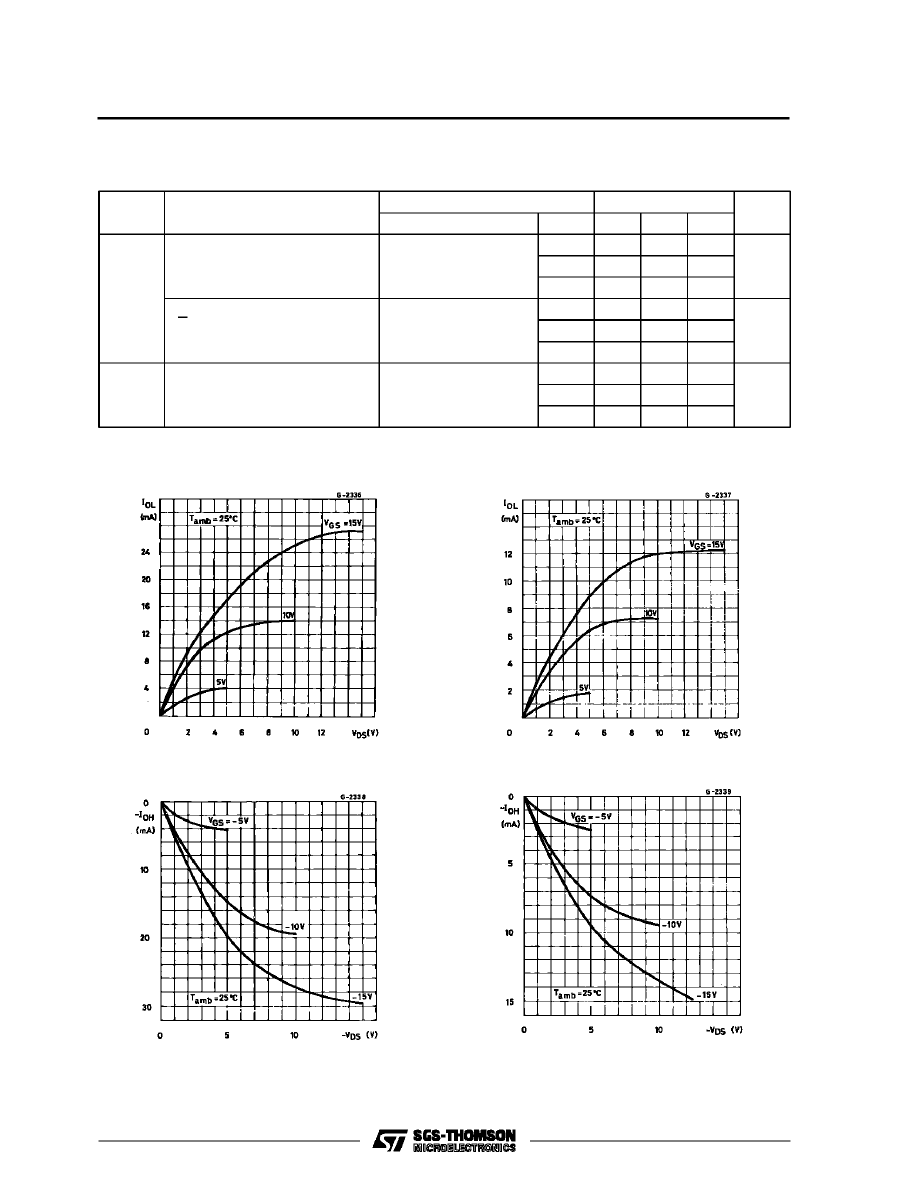
Typical Output Low (sink) Current Characteristics.
Typical Output High (source) Current Charac-
teristics.
Minimum Output High (source) Current Charac-
teristics.
Minimum Output Low (sink) Current Charac-
teristics.
HCC/HCF4555B/4556B
5/14
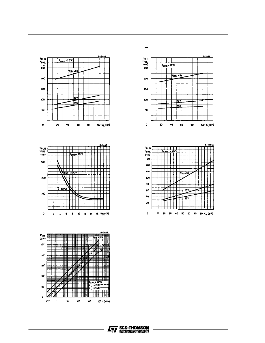
Typical Propagation Delay Time vs. Load Capacit-
ance (A or B input to any output).
Typical Propagation Delay Time vs. Load Capacit-
ance (E input to any input ).
Typical Propagation Delay Time vs. Supply Volt-
age.
Typical Transition Time vs. Load Capacitance.
Typical Dynamic Power Dissipation/per Device
vs. Frequency.
HCC/HCF4555B/4556B
6/14
APPLICATIONS
1 of 8 Decoder using HCC/HCF 4555B
TRUTH TABLE
Inputs
Q Outputs
C
B
A
0
1
2
3
4
5
6
7
0
0
0
1
0
0
0
0
0
0
0
0
0
1
0
1
0
0
0
0
0
0
0
1
0
0
0
1
0
0
0
0
0
0
1
1
0
0
0
1
0
0
0
0
1
0
0
0
0
0
0
1
0
0
0
1
0
1
0
0
0
0
0
1
0
0
1
1
0
0
0
0
0
0
0
1
0
1
1
1
0
0
0
0
0
0
0
1
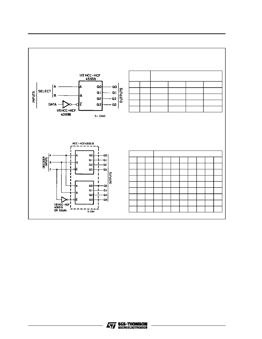
1 of 4 Line Data Demultiplexer using
HCC/HCF4555B
TRUTH TABLE
Select
Inputs
Outputs
B
A
Q 0
Q 1
Q 2
Q 3
0
0
DATA
0
0
0
0
1
0
DATA
0
0
1
0
0
0
DATA
0
1
1
0
0
0
DATA
HCC/HCF4555B/4556B
7/14
APPLICATIONS (continued)
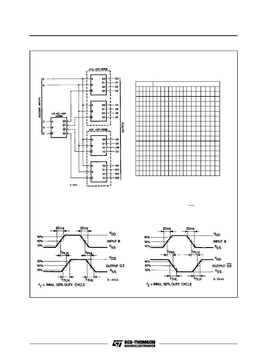
1 of 16 Decoder using HCC/HCF4555B and
HCC/HCF4556B
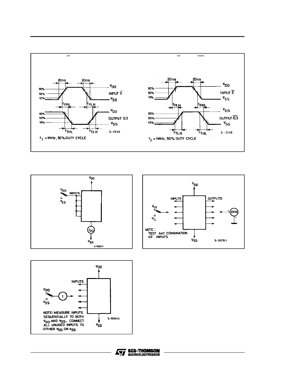
HCC/HCF4555B Input to Q3 Output Dynamic
Signal Waveforms
HCC/HCF4556B Input to Q3 Output Dynamic
Signal Waveforms
X = Don’t care.
TRUT H TABLE
Inputs
Q Outputs
E D C B A 0 1 2 3 4 5 6 7 8 9 1 0 1 1 1 2 1 3 1 4 1 5
0 0 0 0 0 1 0 0 0 0 0 0 0 0 0
0
0
0
0
0
0
0 0 0 0 1 0 1 0 0 0 0 0 0 0 0
0
0
0
0
0
0
0 0 0 1 0 0 0 1 0 0 0 0 0 0 0
0
0
0
0
0
0
0 0 0 1 1 0 0 0 1 0 0 0 0 0 0
0
0
0
0
0
0
0 0 1 0 0 0 0 0 0 1 0 0 0 0 0
0
0
0
0
0
0
0 0 1 0 1 0 0 0 0 0 1 0 0 0 0
0
0
0
0
0
0
0 0 1 1 0 0 0 0 0 0 0 1 0 0 0
0
0
0
0
0
0
0 0 1 1 1 0 0 0 0 0 0 0 1 0 0
0
0
0
0
0
0
0 1 0 0 0 0 0 0 0 0 0 0 0 1 0
0
0
0
0
0
0
0 1 0 0 1 0 0 0 0 0 0 0 0 0 1
0
0
0
0
0
0
0 1 0 1 0 0 0 0 0 0 0 0 0 0 0
1
0
0
0
0
0
0 1 0 1 1 0 0 0 0 0 0 0 0 0 0
0
1
0
0
0
0
0 1 1 0 0 0 0 0 0 0 0 0 0 0 0
0
0
1
0
0
0
0 1 1 0 1 0 0 0 0 0 0 0 0 0 0
0
0
0
1
0
0
0 1 1 1 0 0 0 0 0 0 0 0 0 0 0
0
0
0
0
1
0
0 1 1 1 1 0 0 0 0 0 0 0 0 0 0
0
0
0
0
0
1
1 X X X X 0 0 0 0 0 0 0 0 0 0
0
0
0
0
0
0
HCC/HCF4555B/4556B
8/14
APPLICATIONS (continued)
HCC/HCF4555B E Input to Q3 Output Dynamic
Signal Waveforms
HCC/HCF4556B E Input to Q3 Output Dynamic
Signal Waveforms
TEST CIRCUITS
Quiescien tDevice Current.
Noise Immunity.
Input Leakage Current.
HCC/HCF4555B/4556B
9/14
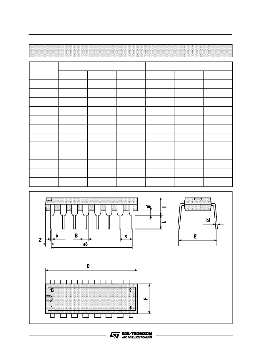
Plastic DIP16 (0.25) MECHANICAL DATA
DIM.
mm
inch
MIN.
TYP.
MAX.
MIN.
TYP.
MAX.
a1
0.51
0.020
B
0.77
1.65
0.030
0.065
b
0.5
0.020
b1
0.25
0.010
D
20
0.787
E
8.5
0.335
e
2.54
0.100
e3
17.78
0.700
F
7.1
0.280
I
5.1
0.201
L
3.3
0.130
Z
1.27
0.050
P001C
HCC/HCF4555B/4556B
10/14
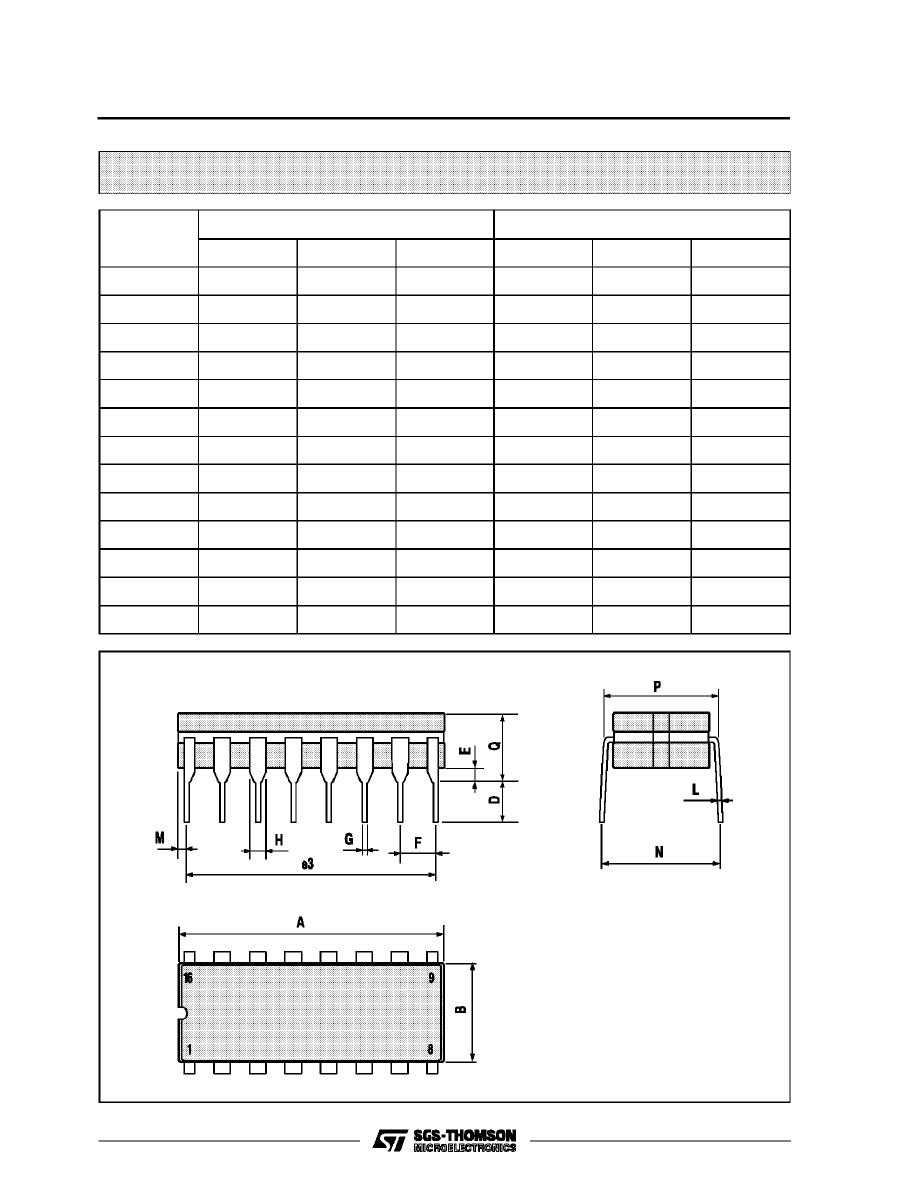
Ceramic DIP16/1 MECHANICAL DATA
DIM.
mm
inch
MIN.
TYP.
MAX.
MIN.
TYP.
MAX.
A
20
0.787
B
7
0.276
D
3.3
0.130
E
0.38
0.015
e3
17.78
0.700
F
2.29
2.79
0.090
0.110
G
0.4
0.55
0.016
0.022
H
1.17
1.52
0.046
0.060
L
0.22
0.31
0.009
0.012
M
0.51
1.27
0.020
0.050
N
10.3
0.406
P
7.8
8.05
0.307
0.317
Q
5.08
0.200
P053D
HCC/HCF4555B/4556B
11/14
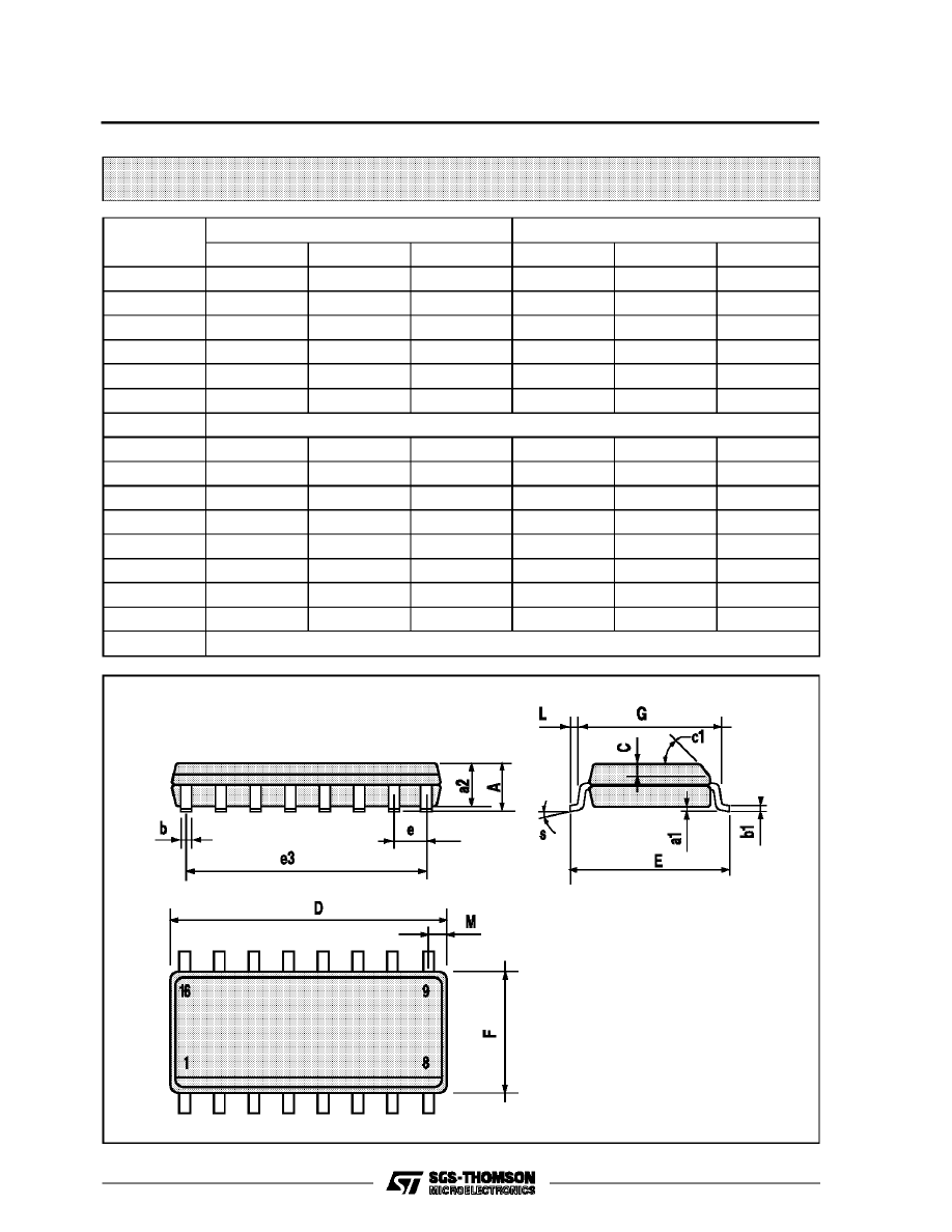
SO16 (Narrow) MECHANICAL DATA
DIM.
mm
inch
MIN.
TYP.
MAX.
MIN.
TYP.
MAX.
A
1.75
0.068
a1
0.1
0.2
0.004
0.007
a2
1.65
0.064
b
0.35
0.46
0.013
0.018
b1
0.19
0.25
0.007
0.010
C
0.5
0.019
c1
45
°
(typ.)
D
9.8
10
0.385
0.393
E
5.8
6.2
0.228
0.244
e
1.27
0.050
e3
8.89
0.350
F
3.8
4.0
0.149
0.157
G
4.6
5.3
0.181
0.208
L
0.5
1.27
0.019
0.050
M
0.62
0.024
S
8
°
(max.)
P013H
HCC/HCF4555B/4556B
12/14
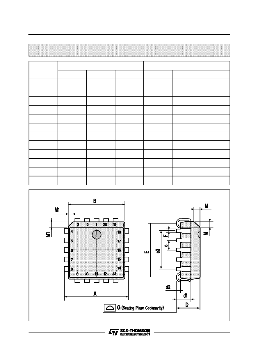
PLCC20 MECHANICAL DATA
DIM.
mm
inch
MIN.
TYP.
MAX.
MIN.
TYP.
MAX.
A
9.78
10.03
0.385
0.395
B
8.89
9.04
0.350
0.356
D
4.2
4.57
0.165
0.180
d1
2.54
0.100
d2
0.56
0.022
E
7.37
8.38
0.290
0.330
e
1.27
0.050
e3
5.08
0.200
F
0.38
0.015
G
0.101
0.004
M
1.27
0.050
M1
1.14
0.045
P027A
HCC/HCF4555B/4556B
13/14

Information furnished is believed to be accurate and reliable. However, SGS-THOMSON Microelectronics assumes no responsability for the
consequences of use of such information nor for any infringement of patents or other rights of third parties which may results from its use. No
license is granted by implication or otherwise under any patent or patent rights of SGS-THOMSON Microelectronics. Specifications mentioned
in this publication are subject to change without notice. This publication supersedes and replaces all information previously supplied.
SGS-THOMSON Microelectronics products are not authorized for use as critical components in life support devices or systems without express
written approval of SGS-THOMSON Microelectonics.
1994 SGS-THOMSON Microelectronics - All Rights Reserved
SGS-THOMSON Microelectronics GROUP OF COMPANIES
Australia - Brazil - France - Germany - Hong Kong - Italy - Japan - Korea - Malaysia - Malta - Morocco - The Netherlands -
Singapore - Spain - Sweden - Switzerland - Taiwan - Thailand - United Kingdom - U.S.A
HCC/HCF4555B/4556B
14/14
Wyszukiwarka
Podobne podstrony:
4555
03 Zasady zachowaniaid 4555 Nieznany (2)
4555
4555
4555
4555
4555
4555
4555
4555
4555 ac
więcej podobnych podstron