2503F–AVR–12/03
Features
•
High-performance, Low-power AVR
®
8-bit Microcontroller
•
Advanced RISC Architecture
– 131 Powerful Instructions – Most Single-clock Cycle Execution
– 32 x 8 General Purpose Working Registers
– Fully Static Operation
– Up to 16 MIPS Throughput at 16 MHz
– On-chip 2-cycle Multiplier
•
Nonvolatile Program and Data Memories
– 32K Bytes of In-System Self-Programmable Flash
Endurance: 10,000 Write/Erase Cycles
– Optional Boot Code Section with Independent Lock Bits
In-System Programming by On-chip Boot Program
True Read-While-Write Operation
– 1024 Bytes EEPROM
Endurance: 100,000 Write/Erase Cycles
– 2K Byte Internal SRAM
– Programming Lock for Software Security
•
JTAG (IEEE std. 1149.1 Compliant) Interface
– Boundary-scan Capabilities According to the JTAG Standard
– Extensive On-chip Debug Support
– Programming of Flash, EEPROM, Fuses, and Lock Bits through the JTAG Interface
•
Peripheral Features
– Two 8-bit Timer/Counters with Separate Prescalers and Compare Modes
– One 16-bit Timer/Counter with Separate Prescaler, Compare Mode, and Capture
Mode
– Real Time Counter with Separate Oscillator
– Four PWM Channels
– 8-channel, 10-bit ADC
8 Single-ended Channels
7 Differential Channels in TQFP Package Only
2 Differential Channels with Programmable Gain at 1x, 10x, or 200x
– Byte-oriented Two-wire Serial Interface
– Programmable Serial USART
– Master/Slave SPI Serial Interface
– Programmable Watchdog Timer with Separate On-chip Oscillator
– On-chip Analog Comparator
•
Special Microcontroller Features
– Power-on Reset and Programmable Brown-out Detection
– Internal Calibrated RC Oscillator
– External and Internal Interrupt Sources
– Six Sleep Modes: Idle, ADC Noise Reduction, Power-save, Power-down, Standby
and Extended Standby
•
I/O and Packages
– 32 Programmable I/O Lines
– 40-pin PDIP, 44-lead TQFP, and 44-pad MLF
•
Operating Voltages
– 2.7 - 5.5V for ATmega32L
– 4.5 - 5.5V for ATmega32
•
Speed Grades
– 0 - 8 MHz for ATmega32L
– 0 - 16 MHz for ATmega32
•
Power Consumption at 1 MHz, 3V, 25
°
C for ATmega32L
– Active: 1.1 mA
– Idle Mode: 0.35 mA
– Power-down Mode: < 1 µA
8-bit
Microcontroller
with 32K Bytes
In-System
Programmable
Flash
ATmega32
ATmega32L
Preliminary
2
ATmega32(L)
2503F–AVR–12/03
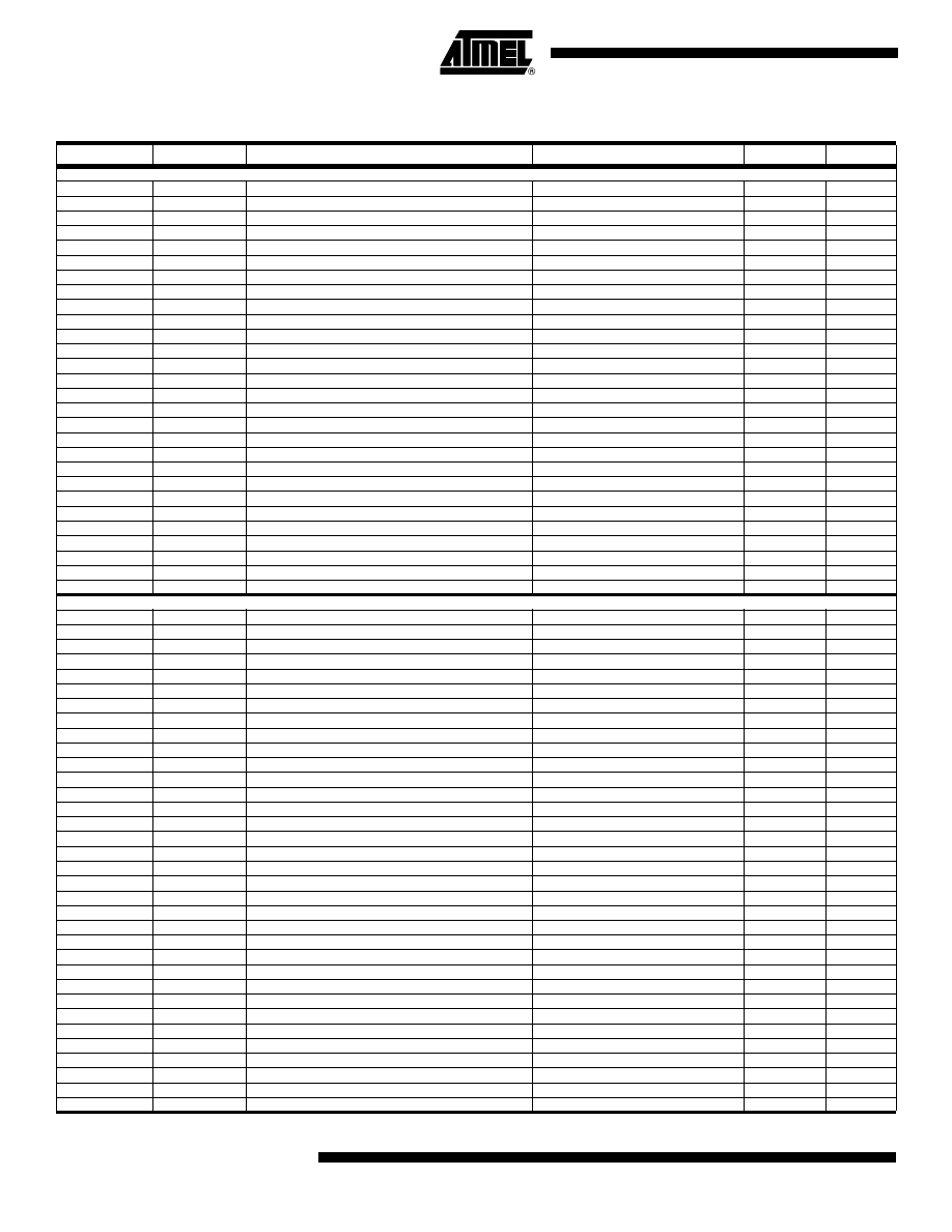
Pin Configurations
Figure 1. Pinouts ATmega32
Disclaimer
Typical values contained in this datasheet are based on simulations and characteriza-
tion of other AVR microcontrollers manufactured on the same process technology. Min
and Max values will be available after the device is characterized.
(XCK/T0) PB0
(T1) PB1
(INT2/AIN0) PB2
(OC0/AIN1) PB3
(SS) PB4
(MOSI) PB5
(MISO) PB6
(SCK) PB7
RESET
VCC
GND
XTAL2
XTAL1
(RXD) PD0
(TXD) PD1
(INT0) PD2
(INT1) PD3
(OC1B) PD4
(OC1A) PD5
(ICP) PD6
PA0 (ADC0)
PA1 (ADC1)
PA2 (ADC2)
PA3 (ADC3)
PA4 (ADC4)
PA5 (ADC5)
PA6 (ADC6)
PA7 (ADC7)
AREF
GND
AVCC
PC7 (TOSC2)
PC6 (TOSC1)
PC5 (TDI)
PC4 (TDO)
PC3 (TMS)
PC2 (TCK)
PC1 (SDA)
PC0 (SCL)
PD7 (OC2)
PA4 (ADC4)
PA5 (ADC5)
PA6 (ADC6)
PA7 (ADC7)
AREF
GND
AVCC
PC7 (TOSC2)
PC6 (TOSC1)
PC5 (TDI)
PC4 (TDO)
(MOSI) PB5
(MISO) PB6
(SCK) PB7
RESET
VCC
GND
XTAL2
XTAL1
(RXD) PD0
(TXD) PD1
(INT0) PD2
(INT1) PD3
(OC1B) PD4
(OC1A) PD5
(ICP) PD6
(OC2) PD7
VCC
GND
(SCL) PC0
(SDA) PC1
(TCK) PC2
(TMS) PC3
PB4 (SS)
PB3 (AIN1/OC0)
PB2 (AIN0/INT2)
PB1 (T1)
PB0 (XCK/T0)
GND
VCC
P
A0 (ADC0)
P
A1 (ADC1)
P
A2 (ADC2)
P
A3 (ADC3)
PDIP
TQFP/MLF
3
ATmega32(L)
2503F–AVR–12/03
Overview
The ATmega32 is a low-power CMOS 8-bit microcontroller based on the AVR enhanced
RISC architecture. By executing powerful instructions in a single clock cycle, the
ATmega32 achieves throughputs approaching 1 MIPS per MHz allowing the system
designer to optimize power consumption versus processing speed.
Block Diagram
Figure 2. Block Diagram
INTERNAL
OSCILLATOR
OSCILLATOR
WATCHDOG
TIMER
MCU CTRL.
& TIMING
OSCILLATOR
TIMERS/
COUNTERS
INTERRUPT
UNIT
STACK
POINTER
EEPROM
SRAM
STATUS
REGISTER
USART
PROGRAM
COUNTER
PROGRAM
FLASH
INSTRUCTION
REGISTER
INSTRUCTION
DECODER
PROGRAMMING
LOGIC
SPI
ADC
INTERFACE
COMP.
INTERFACE
PORTA DRIVERS/BUFFERS
PORTA DIGITAL INTERFACE
GENERAL
PURPOSE
REGISTERS
X
Y
Z
ALU
+
-
PORTC DRIVERS/BUFFERS
PORTC DIGITAL INTERFACE
PORTB DIGITAL INTERFACE
PORTB DRIVERS/BUFFERS
PORTD DIGITAL INTERFACE
PORTD DRIVERS/BUFFERS
XTAL1
XTAL2
RESET
CONTROL
LINES
VCC
GND
MUX &
ADC
AREF
PA0 - PA7
PC0 - PC7
PD0 - PD7
PB0 - PB7
AVR CPU
TWI
AVCC
INTERNAL
CALIBRATED
OSCILLATOR

4
ATmega32(L)
2503F–AVR–12/03
The AVR core combines a rich instruction set with 32 general purpose working registers.
All the 32 registers are directly connected to the Arithmetic Logic Unit (ALU), allowing
two independent registers to be accessed in one single instruction executed in one clock
cycle. The resulting architecture is more code efficient while achieving throughputs up to
ten times faster than conventional CISC microcontrollers.
The ATmega32 provides the following features: 32K bytes of In-System Programmable
Flash Program memory with Read-While-Write capabilities, 1024 bytes EEPROM, 2K
byte SRAM, 32 general purpose I/O lines, 32 general purpose working registers, a
JTAG interface for Boundary-scan, On-chip Debugging support and programming, three
flexible Timer/Counters with compare modes, Internal and External Interrupts, a serial
programmable USART, a byte oriented Two-wire Serial Interface, an 8-channel, 10-bit
ADC with optional differential input stage with programmable gain (TQFP package only),
a programmable Watchdog Timer with Internal Oscillator, an SPI serial port, and six
software selectable power saving modes. The Idle mode stops the CPU while allowing
the USART, Two-wire interface, A/D Converter, SRAM, Timer/Counters, SPI port, and
interrupt system to continue functioning. The Power-down mode saves the register con-
tents but freezes the Oscillator, disabling all other chip functions until the next External
Interrupt or Hardware Reset. In Power-save mode, the Asynchronous Timer continues
to run, allowing the user to maintain a timer base while the rest of the device is sleeping.
The ADC Noise Reduction mode stops the CPU and all I/O modules except Asynchro-
nous Timer and ADC, to minimize switching noise during ADC conversions. In Standby
mode, the crystal/resonator Oscillator is running while the rest of the device is sleeping.
This allows very fast start-up combined with low-power consumption. In Extended
Standby mode, both the main Oscillator and the Asynchronous Timer continue to run.
The device is manufactured using Atmel’s high density nonvolatile memory technology.
The On-chip ISP Flash allows the program memory to be reprogrammed in-system
through an SPI serial interface, by a conventional nonvolatile memory programmer, or
by an On-chip Boot program running on the AVR core. The boot program can use any
interface to download the application program in the Application Flash memory. Soft-
ware in the Boot Flash section will continue to run while the Application Flash section is
updated, providing true Read-While-Write operation. By combining an 8-bit RISC CPU
with In-System Self-Programmable Flash on a monolithic chip, the Atmel ATmega32 is
a powerful microcontroller that provides a highly-flexible and cost-effective solution to
many embedded control applications.
The ATmega32 AVR is supported with a full suite of program and system development
tools including: C compilers, macro assemblers, program debugger/simulators, in-circuit
emulators, and evaluation kits.
Pin Descriptions
VCC
Digital supply voltage.
GND
Ground.
Port A (PA7..PA0)
Port A serves as the analog inputs to the A/D Converter.
Port A also serves as an 8-bit bi-directional I/O port, if the A/D Converter is not used.
Port pins can provide internal pull-up resistors (selected for each bit). The Port A output
buffers have symmetrical drive characteristics with both high sink and source capability.
When pins PA0 to PA7 are used as inputs and are externally pulled low, they will source
current if the internal pull-up resistors are activated. The Port A pins are tri-stated when
a reset condition becomes active, even if the clock is not running.

5
ATmega32(L)
2503F–AVR–12/03
Port B (PB7..PB0)
Port B is an 8-bit bi-directional I/O port with internal pull-up resistors (selected for each
bit). The Port B output buffers have symmetrical drive characteristics with both high sink
and source capability. As inputs, Port B pins that are externally pulled low will source
current if the pull-up resistors are activated. The Port B pins are tri-stated when a reset
condition becomes active, even if the clock is not running.
Port B also serves the functions of various special features of the ATmega32 as listed
on page 55.
Port C (PC7..PC0)
Port C is an 8-bit bi-directional I/O port with internal pull-up resistors (selected for each
bit). The Port C output buffers have symmetrical drive characteristics with both high sink
and source capability. As inputs, Port C pins that are externally pulled low will source
current if the pull-up resistors are activated. The Port C pins are tri-stated when a reset
condition becomes active, even if the clock is not running. If the JTAG interface is
enabled, the pull-up resistors on pins PC5(TDI), PC3(TMS) and PC2(TCK) will be acti-
vated even if a reset occurs.
The TD0 pin is tri-stated unless TAP states that shift out data are entered.
Port C also serves the functions of the JTAG interface and other special features of the
ATmega32 as listed on page 58.
Port D (PD7..PD0)
Port D is an 8-bit bi-directional I/O port with internal pull-up resistors (selected for each
bit). The Port D output buffers have symmetrical drive characteristics with both high sink
and source capability. As inputs, Port D pins that are externally pulled low will source
current if the pull-up resistors are activated. The Port D pins are tri-stated when a reset
condition becomes active, even if the clock is not running.
Port D also serves the functions of various special features of the ATmega32 as listed
on page 60.
RESET
Reset Input. A low level on this pin for longer than the minimum pulse length will gener-
ate a reset, even if the clock is not running. The minimum pulse length is given in Table
15 on page 35. Shorter pulses are not guaranteed to generate a reset.
XTAL1
Input to the inverting Oscillator amplifier and input to the internal clock operating circuit.
XTAL2
Output from the inverting Oscillator amplifier.
AVCC
AVCC is the supply voltage pin for Port A and the A/D Converter. It should be externally
connected to V
CC
, even if the ADC is not used. If the ADC is used, it should be con-
nected to V
CC
through a low-pass filter.
AREF
AREF is the analog reference pin for the A/D Converter.
6
ATmega32(L)
2503F–AVR–12/03
Register Summary
Address
Name
Bit 7
Bit 6
Bit 5
Bit 4
Bit 3
Bit 2
Bit 1
Bit 0
Page
$3F ($5F)
SREG
I
T
H
S
V
N
Z
C
8
$3E ($5E)
SPH
–
–
–
–
SP11
SP10
SP9
SP8
10
$3D ($5D)
SPL
SP7
SP6
SP5
SP4
SP3
SP2
SP1
SP0
10
$3C ($5C)
OCR0
Timer/Counter0 Output Compare Register
80
$3B ($5B)
GICR
INT1
INT0
INT2
–
–
–
IVSEL
IVCE
45, 65
$3A ($5A)
GIFR
INTF1
INTF0
INTF2
–
–
–
–
–
66
$39 ($59)
TIMSK
OCIE2
TOIE2
TICIE1
OCIE1A
OCIE1B
TOIE1
OCIE0
TOIE0
80, 110, 128
$38 ($58)
TIFR
OCF2
TOV2
ICF1
OCF1A
OCF1B
TOV1
OCF0
TOV0
81, 111, 128
$37 ($57)
SPMCR
SPMIE
RWWSB
–
RWWSRE
BLBSET
PGWRT
PGERS
SPMEN
246
$36 ($56)
TWCR
TWINT
TWEA
TWSTA
TWSTO
TWWC
TWEN
–
TWIE
175
$35 ($55)
MCUCR
SE
SM2
SM1
SM0
ISC11
ISC10
ISC01
ISC00
30, 64
$34 ($54)
MCUCSR
JTD
ISC2
–
JTRF
WDRF
BORF
EXTRF
PORF
38, 65, 226
$33 ($53)
TCCR0
FOC0
WGM00
COM01
COM00
WGM01
CS02
CS01
CS00
78
$32 ($52)
TCNT0
Timer/Counter0 (8 Bits)
80
$31
($51)
OSCCAL
Oscillator Calibration Register
28
OCDR
On-Chip Debug Register
222
$30 ($50)
SFIOR
ADTS2
ADTS1
ADTS0
–
ACME
PUD
PSR2
PSR10
54,83,129,196,216
$2F ($4F)
TCCR1A
COM1A1
COM1A0
COM1B1
COM1B0
FOC1A
FOC1B
WGM11
WGM10
105
$2E ($4E)
TCCR1B
ICNC1
ICES1
–
WGM13
WGM12
CS12
CS11
CS10
108
$2D ($4D)
TCNT1H
Timer/Counter1 – Counter Register High Byte
109
$2C ($4C)
TCNT1L
Timer/Counter1 – Counter Register Low Byte
109
$2B ($4B)
OCR1AH
Timer/Counter1 – Output Compare Register A High Byte
109
$2A ($4A)
OCR1AL
Timer/Counter1 – Output Compare Register A Low Byte
109
$29 ($49)
OCR1BH
Timer/Counter1 – Output Compare Register B High Byte
109
$28 ($48)
OCR1BL
Timer/Counter1 – Output Compare Register B Low Byte
109
$27 ($47)
ICR1H
Timer/Counter1 – Input Capture Register High Byte
110
$26 ($46)
ICR1L
Timer/Counter1 – Input Capture Register Low Byte
110
$25 ($45)
TCCR2
FOC2
WGM20
COM21
COM20
WGM21
CS22
CS21
CS20
123
$24 ($44)
TCNT2
Timer/Counter2 (8 Bits)
125
$23 ($43)
OCR2
Timer/Counter2 Output Compare Register
125
$22 ($42)
ASSR
–
–
–
–
AS2
TCN2UB
OCR2UB
TCR2UB
126
$21 ($41)
WDTCR
–
–
–
WDTOE
WDE
WDP2
WDP1
WDP0
40
$20
($40)
UBRRH
URSEL
–
–
–
UBRR[11:8]
162
UCSRC
URSEL
UMSEL
UPM1
UPM0
USBS
UCSZ1
UCSZ0
UCPOL
160
$1F ($3F)
EEARH
–
–
–
–
–
–
EEAR9
EEAR8
17
$1E ($3E)
EEARL
EEPROM Address Register Low Byte
17
$1D ($3D)
EEDR
EEPROM Data Register
17
$1C ($3C)
EECR
–
–
–
–
EERIE
EEMWE
EEWE
EERE
17
$1B ($3B)
PORTA
PORTA7
PORTA6
PORTA5
PORTA4
PORTA3
PORTA2
PORTA1
PORTA0
62
$1A ($3A)
DDRA
DDA7
DDA6
DDA5
DDA4
DDA3
DDA2
DDA1
DDA0
62
$19 ($39)
PINA
PINA7
PINA6
PINA5
PINA4
PINA3
PINA2
PINA1
PINA0
62
$18 ($38)
PORTB
PORTB7
PORTB6
PORTB5
PORTB4
PORTB3
PORTB2
PORTB1
PORTB0
62
$17 ($37)
DDRB
DDB7
DDB6
DDB5
DDB4
DDB3
DDB2
DDB1
DDB0
62
$16 ($36)
PINB
PINB7
PINB6
PINB5
PINB4
PINB3
PINB2
PINB1
PINB0
63
$15 ($35)
PORTC
PORTC7
PORTC6
PORTC5
PORTC4
PORTC3
PORTC2
PORTC1
PORTC0
63
$14 ($34)
DDRC
DDC7
DDC6
DDC5
DDC4
DDC3
DDC2
DDC1
DDC0
63
$13 ($33)
PINC
PINC7
PINC6
PINC5
PINC4
PINC3
PINC2
PINC1
PINC0
63
$12 ($32)
PORTD
PORTD7
PORTD6
PORTD5
PORTD4
PORTD3
PORTD2
PORTD1
PORTD0
63
$11 ($31)
DDRD
DDD7
DDD6
DDD5
DDD4
DDD3
DDD2
DDD1
DDD0
63
$10 ($30)
PIND
PIND7
PIND6
PIND5
PIND4
PIND3
PIND2
PIND1
PIND0
63
$0F ($2F)
SPDR
SPI Data Register
136
$0E ($2E)
SPSR
SPIF
WCOL
–
–
–
–
–
SPI2X
136
$0D ($2D)
SPCR
SPIE
SPE
DORD
MSTR
CPOL
CPHA
SPR1
SPR0
134
$0C ($2C)
UDR
USART I/O Data Register
157
$0B ($2B)
UCSRA
RXC
TXC
UDRE
FE
DOR
PE
U2X
MPCM
158
$0A ($2A)
UCSRB
RXCIE
TXCIE
UDRIE
RXEN
TXEN
UCSZ2
RXB8
TXB8
159
$09 ($29)
UBRRL
USART Baud Rate Register Low Byte
162
$08 ($28)
ACSR
ACD
ACBG
ACO
ACI
ACIE
ACIC
ACIS1
ACIS0
197
$07 ($27)
ADMUX
REFS1
REFS0
ADLAR
MUX4
MUX3
MUX2
MUX1
MUX0
212
$06 ($26)
ADCSRA
ADEN
ADSC
ADATE
ADIF
ADIE
ADPS2
ADPS1
ADPS0
214
$05 ($25)
ADCH
ADC Data Register High Byte
215
$04 ($24)
ADCL
ADC Data Register Low Byte
215
$03 ($23)
TWDR
Two-wire Serial Interface Data Register
177
$02 ($22)
TWAR
TWA6
TWA5
TWA4
TWA3
TWA2
TWA1
TWA0
TWGCE
177

7
ATmega32(L)
2503F–AVR–12/03
Notes:
1. When the OCDEN Fuse is unprogrammed, the OSCCAL Register is always accessed on this address. Refer to the debug-
ger specific documentation for details on how to use the OCDR Register.
2. Refer to the USART description for details on how to access UBRRH and UCSRC.
3. For compatibility with future devices, reserved bits should be written to zero if accessed. Reserved I/O memory addresses
should never be written.
4. Some of the Status Flags are cleared by writing a logical one to them. Note that the CBI and SBI instructions will operate on
all bits in the I/O Register, writing a one back into any flag read as set, thus clearing the flag. The CBI and SBI instructions
work with registers $00 to $1F only.
$01 ($21)
TWSR
TWS7
TWS6
TWS5
TWS4
TWS3
–
TWPS1
TWPS0
176
$00 ($20)
TWBR
Two-wire Serial Interface Bit Rate Register
175
Address
Name
Bit 7
Bit 6
Bit 5
Bit 4
Bit 3
Bit 2
Bit 1
Bit 0
Page
8
ATmega32(L)
2503F–AVR–12/03
Instruction Set Summary
Mnemonics
Operands
Description
Operation
Flags
#Clocks
ARITHMETIC AND LOGIC INSTRUCTIONS
ADD
Rd, Rr
Add two Registers
Rd
←
Rd + Rr
Z,C,N,V,H
1
ADC
Rd, Rr
Add with Carry two Registers
Rd
←
Rd + Rr + C
Z,C,N,V,H
1
ADIW
Rdl,K
Add Immediate to Word
Rdh:Rdl
←
Rdh:Rdl + K
Z,C,N,V,S
2
SUB
Rd, Rr
Subtract two Registers
Rd
←
Rd - Rr
Z,C,N,V,H
1
SUBI
Rd, K
Subtract Constant from Register
Rd
←
Rd - K
Z,C,N,V,H
1
SBC
Rd, Rr
Subtract with Carry two Registers
Rd
←
Rd - Rr - C
Z,C,N,V,H
1
SBCI
Rd, K
Subtract with Carry Constant from Reg.
Rd
←
Rd - K - C
Z,C,N,V,H
1
SBIW
Rdl,K
Subtract Immediate from Word
Rdh:Rdl
←
Rdh:Rdl - K
Z,C,N,V,S
2
AND
Rd, Rr
Logical AND Registers
Rd
←
Rd
•
Rr
Z,N,V
1
ANDI
Rd, K
Logical AND Register and Constant
Rd
←
Rd
•
K
Z,N,V
1
OR
Rd, Rr
Logical OR Registers
Rd
←
Rd v Rr
Z,N,V
1
ORI
Rd, K
Logical OR Register and Constant
Rd
←
Rd v K
Z,N,V
1
EOR
Rd, Rr
Exclusive OR Registers
Rd
←
Rd
⊕
Rr
Z,N,V
1
COM
Rd
One’s Complement
Rd
←
$FF
−
Rd
Z,C,N,V
1
NEG
Rd
Two’s Complement
Rd
←
$00
−
Rd
Z,C,N,V,H
1
SBR
Rd,K
Set Bit(s) in Register
Rd
←
Rd v K
Z,N,V
1
CBR
Rd,K
Clear Bit(s) in Register
Rd
←
Rd
•
($FF - K)
Z,N,V
1
INC
Rd
Increment
Rd
←
Rd + 1
Z,N,V
1
DEC
Rd
Decrement
Rd
←
Rd
−
1
Z,N,V
1
TST
Rd
Test for Zero or Minus
Rd
←
Rd
•
Rd
Z,N,V
1
CLR
Rd
Clear Register
Rd
←
Rd
⊕
Rd
Z,N,V
1
SER
Rd
Set Register
Rd
←
$FF
None
1
MUL
Rd, Rr
Multiply Unsigned
R1:R0
←
Rd x Rr
Z,C
2
MULS
Rd, Rr
Multiply Signed
R1:R0
←
Rd x Rr
Z,C
2
MULSU
Rd, Rr
Multiply Signed with Unsigned
R1:R0
←
Rd x Rr
Z,C
2
FMUL
Rd, Rr
Fractional Multiply Unsigned
R1:R0
←
(Rd x Rr)
<< 1
Z,C
2
FMULS
Rd, Rr
Fractional Multiply Signed
R1:R0
←
(Rd x Rr)
<< 1
Z,C
2
FMULSU
Rd, Rr
Fractional Multiply Signed with Unsigned
R1:R0
←
(Rd x Rr)
<< 1
Z,C
2
BRANCH INSTRUCTIONS
RJMP
k
Relative Jump
PC
←
PC + k + 1
None
2
IJMP
Indirect Jump to (Z)
PC
←
Z
None
2
JMP
k
Direct Jump
PC
←
k
None
3
RCALL
k
Relative Subroutine Call
PC
←
PC + k + 1
None
3
ICALL
Indirect Call to (Z)
PC
←
Z
None
3
CALL
k
Direct Subroutine Call
PC
←
k
None
4
RET
Subroutine Return
PC
←
Stack
None
4
RETI
Interrupt Return
PC
←
Stack
I
4
CPSE
Rd,Rr
Compare, Skip if Equal
if (Rd = Rr) PC
←
PC + 2 or 3
None
1 / 2 / 3
CP
Rd,Rr
Compare
Rd
−
Rr
Z, N,V,C,H
1
CPC
Rd,Rr
Compare with Carry
Rd
−
Rr
−
C
Z, N,V,C,H
1
CPI
Rd,K
Compare Register with Immediate
Rd
−
K
Z, N,V,C,H
1
SBRC
Rr, b
Skip if Bit in Register Cleared
if (Rr(b)=0) PC
←
PC + 2 or 3
None
1 / 2 / 3
SBRS
Rr, b
Skip if Bit in Register is Set
if (Rr(b)=1) PC
←
PC + 2 or 3
None
1 / 2 / 3
SBIC
P, b
Skip if Bit in I/O Register Cleared
if (P(b)=0) PC
←
PC + 2 or 3
None
1 / 2 / 3
SBIS
P, b
Skip if Bit in I/O Register is Set
if (P(b)=1) PC
←
PC + 2 or 3
None
1 / 2 / 3
BRBS
s, k
Branch if Status Flag Set
if (SREG(s) = 1) then PC
←
PC+k + 1
None
1 / 2
BRBC
s, k
Branch if Status Flag Cleared
if (SREG(s) = 0) then PC
←
PC+k + 1
None
1 / 2
BREQ
k
Branch if Equal
if (Z = 1) then PC
←
PC + k + 1
None
1 / 2
BRNE
k
Branch if Not Equal
if (Z = 0) then PC
←
PC + k + 1
None
1 / 2
BRCS
k
Branch if Carry Set
if (C = 1) then PC
←
PC + k + 1
None
1 / 2
BRCC
k
Branch if Carry Cleared
if (C = 0) then PC
←
PC + k + 1
None
1 / 2
BRSH
k
Branch if Same or Higher
if (C = 0) then PC
←
PC + k + 1
None
1 / 2
BRLO
k
Branch if Lower
if (C = 1) then PC
←
PC + k + 1
None
1 / 2
BRMI
k
Branch if Minus
if (N = 1) then PC
←
PC + k + 1
None
1 / 2
BRPL
k
Branch if Plus
if (N = 0) then PC
←
PC + k + 1
None
1 / 2
BRGE
k
Branch if Greater or Equal, Signed
if (N
⊕
V= 0) then PC
←
PC + k + 1
None
1 / 2
BRLT
k
Branch if Less Than Zero, Signed
if (N
⊕
V= 1) then PC
←
PC + k + 1
None
1 / 2
BRHS
k
Branch if Half Carry Flag Set
if (H = 1) then PC
←
PC + k + 1
None
1 / 2
BRHC
k
Branch if Half Carry Flag Cleared
if (H = 0) then PC
←
PC + k + 1
None
1 / 2
BRTS
k
Branch if T Flag Set
if (T = 1) then PC
←
PC + k + 1
None
1 / 2
BRTC
k
Branch if T Flag Cleared
if (T = 0) then PC
←
PC + k + 1
None
1 / 2
BRVS
k
Branch if Overflow Flag is Set
if (V = 1) then PC
←
PC + k + 1
None
1 / 2
BRVC
k
Branch if Overflow Flag is Cleared
if (V = 0) then PC
←
PC + k + 1
None
1 / 2
9
ATmega32(L)
2503F–AVR–12/03
BRIE
k
Branch if Interrupt Enabled
if ( I = 1) then PC
←
PC + k + 1
None
1 / 2
BRID
k
Branch if Interrupt Disabled
if ( I = 0) then PC
←
PC + k + 1
None
1 / 2
DATA TRANSFER INSTRUCTIONS
MOV
Rd, Rr
Move Between Registers
Rd
←
Rr
None
1
MOVW
Rd, Rr
Copy Register Word
Rd+1:Rd
←
Rr+1:Rr
None
1
LDI
Rd, K
Load Immediate
Rd
←
K
None
1
LD
Rd, X
Load Indirect
Rd
←
(X)
None
2
LD
Rd, X+
Load Indirect and Post-Inc.
Rd
←
(X), X
←
X + 1
None
2
LD
Rd, - X
Load Indirect and Pre-Dec.
X
←
X - 1, Rd
←
(X)
None
2
LD
Rd, Y
Load Indirect
Rd
←
(Y)
None
2
LD
Rd, Y+
Load Indirect and Post-Inc.
Rd
←
(Y), Y
←
Y + 1
None
2
LD
Rd, - Y
Load Indirect and Pre-Dec.
Y
←
Y - 1, Rd
←
(Y)
None
2
LDD
Rd,Y+q
Load Indirect with Displacement
Rd
←
(Y + q)
None
2
LD
Rd, Z
Load Indirect
Rd
←
(Z)
None
2
LD
Rd, Z+
Load Indirect and Post-Inc.
Rd
←
(Z), Z
←
Z+1
None
2
LD
Rd, -Z
Load Indirect and Pre-Dec.
Z
←
Z - 1, Rd
←
(Z)
None
2
LDD
Rd, Z+q
Load Indirect with Displacement
Rd
←
(Z + q)
None
2
LDS
Rd, k
Load Direct from SRAM
Rd
←
(k)
None
2
ST
X, Rr
Store Indirect
(X)
←
Rr
None
2
ST
X+, Rr
Store Indirect and Post-Inc.
(X)
←
Rr, X
←
X + 1
None
2
ST
- X, Rr
Store Indirect and Pre-Dec.
X
←
X - 1, (X)
←
Rr
None
2
ST
Y, Rr
Store Indirect
(Y)
←
Rr
None
2
ST
Y+, Rr
Store Indirect and Post-Inc.
(Y)
←
Rr, Y
←
Y + 1
None
2
ST
- Y, Rr
Store Indirect and Pre-Dec.
Y
←
Y - 1, (Y)
←
Rr
None
2
STD
Y+q,Rr
Store Indirect with Displacement
(Y + q)
←
Rr
None
2
ST
Z, Rr
Store Indirect
(Z)
←
Rr
None
2
ST
Z+, Rr
Store Indirect and Post-Inc.
(Z)
←
Rr, Z
←
Z + 1
None
2
ST
-Z, Rr
Store Indirect and Pre-Dec.
Z
←
Z - 1, (Z)
←
Rr
None
2
STD
Z+q,Rr
Store Indirect with Displacement
(Z + q)
←
Rr
None
2
STS
k, Rr
Store Direct to SRAM
(k)
←
Rr
None
2
LPM
Load Program Memory
R0
←
(Z)
None
3
LPM
Rd, Z
Load Program Memory
Rd
←
(Z)
None
3
LPM
Rd, Z+
Load Program Memory and Post-Inc
Rd
←
(Z), Z
←
Z+1
None
3
SPM
Store Program Memory
(Z)
←
R1:R0
None
-
IN
Rd, P
In Port
Rd
←
P
None
1
OUT
P, Rr
Out Port
P
←
Rr
None
1
PUSH
Rr
Push Register on Stack
Stack
←
Rr
None
2
POP
Rd
Pop Register from Stack
Rd
←
Stack
None
2
BIT AND BIT-TEST INSTRUCTIONS
SBI
P,b
Set Bit in I/O Register
I/O(P,b)
←
1
None
2
CBI
P,b
Clear Bit in I/O Register
I/O(P,b)
←
0
None
2
LSL
Rd
Logical Shift Left
Rd(n+1)
←
Rd(n), Rd(0)
←
0
Z,C,N,V
1
LSR
Rd
Logical Shift Right
Rd(n)
←
Rd(n+1), Rd(7)
←
0
Z,C,N,V
1
ROL
Rd
Rotate Left Through Carry
Rd(0)
←
C,Rd(n+1)
←
Rd(n),C
←
Rd(7)
Z,C,N,V
1
ROR
Rd
Rotate Right Through Carry
Rd(7)
←
C,Rd(n)
←
Rd(n+1),C
←
Rd(0)
Z,C,N,V
1
ASR
Rd
Arithmetic Shift Right
Rd(n)
←
Rd(n+1), n=0..6
Z,C,N,V
1
SWAP
Rd
Swap Nibbles
Rd(3..0)
←
Rd(7..4),Rd(7..4)
←
Rd(3..0)
None
1
BSET
s
Flag Set
SREG(s)
←
1
SREG(s)
1
BCLR
s
Flag Clear
SREG(s)
←
0
SREG(s)
1
BST
Rr, b
Bit Store from Register to T
T
←
Rr(b)
T
1
BLD
Rd, b
Bit load from T to Register
Rd(b)
←
T
None
1
SEC
Set Carry
C
←
1
C
1
CLC
Clear Carry
C
←
0
C
1
SEN
Set Negative Flag
N
←
1
N
1
CLN
Clear Negative Flag
N
←
0
N
1
SEZ
Set Zero Flag
Z
←
1
Z
1
CLZ
Clear Zero Flag
Z
←
0
Z
1
SEI
Global Interrupt Enable
I
←
1
I
1
CLI
Global Interrupt Disable
I
←
0
I
1
SES
Set Signed Test Flag
S
←
1
S
1
CLS
Clear Signed Test Flag
S
←
0
S
1
SEV
Set Twos Complement Overflow.
V
←
1
V
1
CLV
Clear Twos Complement Overflow
V
←
0
V
1
SET
Set T in SREG
T
←
1
T
1
CLT
Clear T in SREG
T
←
0
T
1
SEH
Set Half Carry Flag in SREG
H
←
1
H
1
Mnemonics
Operands
Description
Operation
Flags
#Clocks

10
ATmega32(L)
2503F–AVR–12/03
CLH
Clear Half Carry Flag in SREG
H
←
0
H
1
MCU CONTROL INSTRUCTIONS
NOP
No Operation
None
1
SLEEP
Sleep
(see specific descr. for Sleep function)
None
1
WDR
Watchdog Reset
(see specific descr. for WDR/timer)
None
1
BREAK
Break
For On-Chip Debug Only
None
N/A
Mnemonics
Operands
Description
Operation
Flags
#Clocks
11
ATmega32(L)
2503F–AVR–12/03
Ordering Information
Speed (MHz)
Power Supply
Ordering Code
Package
Operation Range
8
2.7 - 5.5V
ATmega32L-8AC
ATmega32L-8PC
ATmega32L-8MC
44A
40P6
44M1
Commercial
(0
o
C to 70
o
C)
ATmega32L-8AI
ATmega32L-8PI
ATmega32L-8MI
44A
40P6
44M1
Industrial
(-40
o
C to 85
o
C)
16
4.5 - 5.5V
ATmega32-16AC
ATmega32-16PC
ATmega32-16MI
44A
40P6
44M1
Commercial
(0
o
C to 70
o
C)
ATmega32-16AI
ATmega32-16PI
ATmega32-16MC
44A
40P6
44M1
Industrial
(-40
o
C to 85
o
C)
Package Type
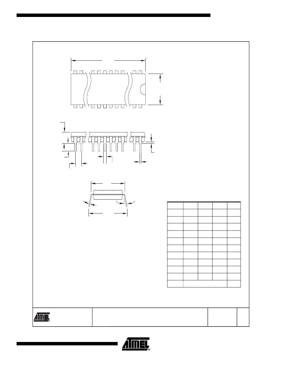
44A
44-lead, Thin (1.0 mm) Plastic Gull Wing Quad Flat Package (TQFP)
40P6
40-pin, 0.600” Wide, Plastic Dual Inline Package (PDIP)
44M1
44-pad, 7 x 7 x 1.0 mm body, lead pitch 0.50 mm, Micro Lead Frame Package (MLF)
12
ATmega32(L)
2503F–AVR–12/03
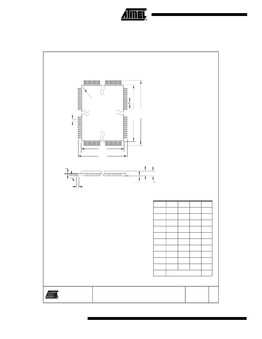
Packaging Information
44A
2325 Orchard Parkway
San Jose, CA 95131
TITLE
DRAWING NO.
R
REV.
44A, 44-lead, 10 x 10 mm Body Size, 1.0 mm Body Thickness,
0.8 mm Lead Pitch, Thin Profile Plastic Quad Flat Package (TQFP)
B
44A
10/5/2001
PIN 1 IDENTIFIER
0˚~7˚
PIN 1
L
C
A1
A2
A
D1
D
e
E1
E
B
COMMON DIMENSIONS
(Unit of Measure = mm)
SYMBOL
MIN
NOM
MAX
NOTE
Notes:
1. This package conforms to JEDEC reference MS-026, Variation ACB.
2. Dimensions D1 and E1 do not include mold protrusion. Allowable
protrusion is 0.25 mm per side. Dimensions D1 and E1 are maximum
plastic body size dimensions including mold mismatch.
3. Lead coplanarity is 0.10 mm maximum.
A
–
–
1.20
A1
0.05
–
0.15
A2
0.95
1.00
1.05
D
11.75
12.00
12.25
D1
9.90
10.00
10.10
Note 2
E
11.75
12.00
12.25
E1
9.90
10.00
10.10
Note 2
B 0.30
–
0.45
C
0.09
–
0.20
L
0.45
–
0.75
e
0.80 TYP
13
ATmega32(L)
2503F–AVR–12/03
40P6
2325 Orchard Parkway
San Jose, CA 95131
TITLE
DRAWING NO.
R
REV.
40P6, 40-lead (0.600"/15.24 mm Wide) Plastic Dual
Inline Package (PDIP)
B
40P6
09/28/01
PIN
1
E1
A1
B
REF
E
B1
C
L
SEATING PLANE
A
0º ~ 15º
D
e
eB
COMMON DIMENSIONS
(Unit of Measure = mm)
SYMBOL
MIN
NOM
MAX
NOTE
A
–
–
4.826
A1
0.381
–
–
D
52.070
–
52.578
Note 2
E
15.240
–
15.875
E1
13.462
–
13.970
Note 2
B
0.356
–
0.559
B1
1.041
–
1.651
L
3.048
–
3.556
C
0.203
–
0.381
eB
15.494
–
17.526
e
2.540 TYP
Notes:
1. This package conforms to JEDEC reference MS-011, Variation AC.
2. Dimensions D and E1 do not include mold Flash or Protrusion.
Mold Flash or Protrusion shall not exceed 0.25 mm (0.010").
14
ATmega32(L)
2503F–AVR–12/03
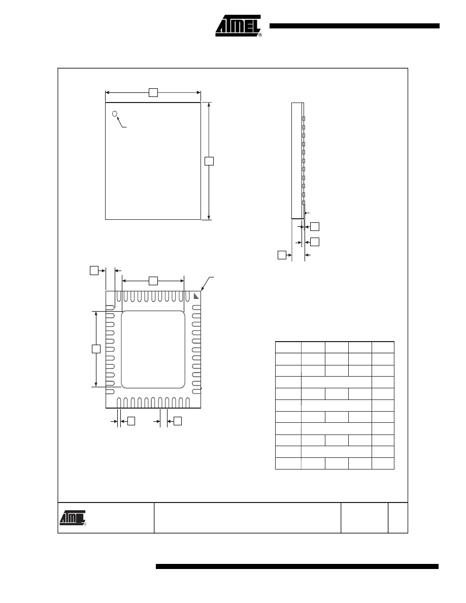
44M1
2325 Orchard Parkway
San Jose, CA 95131
TITLE
DRAWING NO.
R
REV.
44M1, 44-pad, 7 x 7 x 1.0 mm Body, Lead Pitch 0.50 mm
Micro Lead Frame Package (MLF)
C
44M1
01/15/03
COMMON DIMENSIONS
(Unit of Measure = mm)
SYMBOL
MIN
NOM
MAX
NOTE
A
0.80
0.90
1.00
A1
–
0.02
0.05
A3
0.25 REF
b
0.18
0.23
0.30
D
7.00 BSC
D2
5.00
5.20
5.40
E
7.00 BSC
E2
5.00
5.20
5.40
e
0.50 BSC
L
0.35
0.55
0.75
Notes: 1. JEDEC Standard MO-220, Fig. 1 (SAW Singulation) VKKD-1.
TOP VIEW
SIDE VIEW
BOTTOM VIEW
D
E
Marked Pin# 1 ID
E2
D2
b
e
Pin #1 Corner
L
A1
A3
A
SEATING PLANE

15
ATmega32(L)
2503F–AVR–12/03
Errata
ATmega32 Rev. A
There are no errata for this revision of ATmega32.However, a proposal for solving prob-
lems regarding the JTAG instruction IDCODE is presented below.
IDCODE masks data from TDI input
The public but optional JTAG instruction IDCODE is not implemented correctly
according to IEEE1149.1; a logic one is scanned into the shift register instead of the
TDI input while shifting the Device ID Register. Hence, captured data from the pre-
ceding devices in the boundary scan chain are lost and replaced by all-ones, and
data to succeeding devices are replaced by all-ones during Update-DR.
If ATmega32 is the only device in the scan chain, the problem is not visible.
Problem Fix / Workaround
Select the Device ID Register of the ATmega32 (Either by issuing the IDCODE
instruction or by entering the Test-Logic-Reset state of the TAP controller) to read
out the contents of its Device ID Register and possibly data from succeeding
devices of the scan chain. Note that data to succeeding devices cannot be entered
during this scan, but data to preceding devices can. Issue the BYPASS instruction
to the ATmega32 to select its Bypass Register while reading the Device ID Regis-
ters of preceding devices of the boundary scan chain. Never read data from
succeeding devices in the boundary scan chain or upload data to the succeeding
devices while the Device ID Register is selected for the ATmega32. Note that the
IDCODE instruction is the default instruction selected by the Test-Logic-Reset state
of the TAP-controller.
Alternative Problem Fix / Workaround
If the Device IDs of all devices in the boundary scan chain must be captured simul-
taneously (for instance if blind interrogation is used), the boundary scan chain can
be connected in such way that the ATmega32 is the fist device in the chain. Update-
DR will still not work for the succeeding devices in the boundary scan chain as long
as IDCODE is present in the JTAG Instruction Register, but the Device ID registered
cannot be uploaded in any case.

16
ATmega32(L)
2503F–AVR–12/03
Datasheet Change
Log for ATmega32
Please note that the referring page numbers in this section are referred to this docu-
ment. The referring revision in this section are referring to the document revision.
Changes from Rev.
2503E-09/03 to Rev.
2503F-12/03
1.
Updated “Calibrated Internal RC Oscillator” on page 27.
Changes from Rev.
2503D-02/03 to Rev.
2503E-09/03
1.
Updated and changed “On-chip Debug System” to “JTAG Interface and On-
chip Debug System” on page 33.
2.
Updated Table 15 on page 35.
3.
Updated “Test Access Port – TAP” on page 217 regarding the JTAGEN fuse.
4.
Updated description for Bit 7 – JTD: JTAG Interface Disable on page 226.
5.
Added a note regarding JTAGEN fuse to Table 105 on page 255.
6.
Updated Absolute Maximum Ratings* , DC Characteristics and ADC Charac-
teristics in “Electrical Characteristics” on page 285.
7.
Added a proposal for solving problems regarding the JTAG instruction
IDCODE in “Errata” on page 15.
Changes from Rev.
2503C-10/02 to Rev.
2503D-02/03
1.
Added EEAR9 in EEARH in “Register Summary” on page 6.
2.
Added Chip Erase as a first step in“Programming the Flash” on page 282 and
“Programming the EEPROM” on page 283.
3.
Removed reference to “Multi-purpose Oscillator” application note and
“32 kHz Crystal Oscillator” application note, which do not exist.
4.
Added information about PWM symmetry for Timer0 and Timer2.
5.
Added note in “Filling the Temporary Buffer (Page Loading)” on page 249
about writing to the EEPROM during an SPM Page Load.
6.
Added “Power Consumption” data in “Features” on page 1.
7.
Added section “EEPROM Write During Power-down Sleep Mode” on page 20.
8.
Added note about Differential Mode with Auto Triggering in “Prescaling and
Conversion Timing” on page 202.
9.
Updated Table 90 on page 230.
10.Added updated “Packaging Information” on page 12.
Changes from Rev.
2503B-10/02 to Rev.
2503C-10/02
1.
Updated the “DC Characteristics” on page 285.

17
ATmega32(L)
2503F–AVR–12/03
Changes from Rev.
2503A-03/02 to Rev.
2503B-10/02
1.
Canged the endurance on the Flash to 10,000 Write/Erase Cycles.
2.
Bit nr.4 – ADHSM – in SFIOR Register removed.
3.
Added the section “Default Clock Source” on page 23.
4.
When using External Clock there are some limitations regards to change of
frequency. This is described in “External Clock” on page 29 and Table 118 on
page 287.
5.
Added a sub section regarding OCD-system and power consumption in the
section “Minimizing Power Consumption” on page 32.
6.
Corrected typo (WGM-bit setting) for:
– “Fast PWM Mode” on page 73 (Timer/Counter0)
– “Phase Correct PWM Mode” on page 74 (Timer/Counter0)
– “Fast PWM Mode” on page 118 (Timer/Counter2)
– “Phase Correct PWM Mode” on page 119 (Timer/Counter2)
7.
Corrected Table 67 on page 162 (USART).
8.
Updated V
IL
, I
IL
, and I
IH
parameter in “DC Characteristics” on page 285.
9.
Updated Description of OSCCAL Calibration Byte.
In the datasheet, it was not explained how to take advantage of the calibration bytes
for 2, 4, and 8 MHz Oscillator selections. This is now added in the following
sections:
Improved description of “Oscillator Calibration Register – OSCCAL” on page 28 and
“Calibration Byte” on page 256.
10. Corrected typo in Table 42.
11. Corrected description in Table 45 and Table 46.
12. Updated Table 119, Table 121, and Table 122.

Printed on recycled paper.
Disclaimer: Atmel Corporation makes no warranty for the use of its products, other than those expressly contained in the Company’s standard
warranty which is detailed in Atmel’s Terms and Conditions located on the Company’s web site. The Company assumes no responsibility for any
errors which may appear in this document, reserves the right to change devices or specifications detailed herein at any time without notice, and
does not make any commitment to update the information contained herein. No licenses to patents or other intellectual property of Atmel are
granted by the Company in connection with the sale of Atmel products, expressly or by implication. Atmel’s products are not authorized for use
as critical components in life support devices or systems.
Atmel Corporation
Atmel Operations
2325 Orchard Parkway
San Jose, CA 95131, USA
Tel: 1(408) 441-0311
Fax: 1(408) 487-2600
Regional Headquarters
Europe
Atmel Sarl
Route des Arsenaux 41
Case Postale 80
CH-1705 Fribourg
Switzerland
Tel: (41) 26-426-5555
Fax: (41) 26-426-5500
Asia
Room 1219
Chinachem Golden Plaza
77 Mody Road Tsimshatsui
East Kowloon
Hong Kong
Tel: (852) 2721-9778
Fax: (852) 2722-1369
Japan
9F, Tonetsu Shinkawa Bldg.
1-24-8 Shinkawa
Chuo-ku, Tokyo 104-0033
Japan
Tel: (81) 3-3523-3551
Fax: (81) 3-3523-7581
Memory
2325 Orchard Parkway
San Jose, CA 95131, USA
Tel: 1(408) 441-0311
Fax: 1(408) 436-4314
Microcontrollers
2325 Orchard Parkway
San Jose, CA 95131, USA
Tel: 1(408) 441-0311
Fax: 1(408) 436-4314
La Chantrerie
BP 70602
44306 Nantes Cedex 3, France
Tel: (33) 2-40-18-18-18
Fax: (33) 2-40-18-19-60
ASIC/ASSP/Smart Cards
Zone Industrielle
13106 Rousset Cedex, France
Tel: (33) 4-42-53-60-00
Fax: (33) 4-42-53-60-01
1150 East Cheyenne Mtn. Blvd.
Colorado Springs, CO 80906, USA
Tel: 1(719) 576-3300
Fax: 1(719) 540-1759
Scottish Enterprise Technology Park
Maxwell Building
East Kilbride G75 0QR, Scotland
Tel: (44) 1355-803-000
Fax: (44) 1355-242-743
RF/Automotive
Theresienstrasse 2
Postfach 3535
74025 Heilbronn, Germany
Tel: (49) 71-31-67-0
Fax: (49) 71-31-67-2340
1150 East Cheyenne Mtn. Blvd.
Colorado Springs, CO 80906, USA
Tel: 1(719) 576-3300
Fax: 1(719) 540-1759
Biometrics/Imaging/Hi-Rel MPU/
High Speed Converters/RF Datacom
Avenue de Rochepleine
BP 123
38521 Saint-Egreve Cedex, France
Tel: (33) 4-76-58-30-00
Fax: (33) 4-76-58-34-80
Literature Requests
www.atmel.com/literature
2503F–AVR–12/03
© Atmel Corporation 2003. All rights reserved. Atmel
®
and combinations thereof, AVR
®
, and AVR Studio
®
are the registered trademarks of
Atmel Corporation or its subsidiaries. Microsoft
®
, Windows
®
, Windows NT
®
, and Windows XP
®
are the registered trademarks of Microsoft Corpo-
ration. Other terms and product names may be the trademarks of others

This datasheet has been download from:
Datasheets for electronics components.
Document Outline
- Features
- Pin Configurations
- Disclaimer
- Overview
- Register Summary
- Instruction Set Summary
- Ordering Information
- Packaging Information
- Errata
- Datasheet Change Log for ATmega32
Wyszukiwarka
Podobne podstrony:
Atmega 64 opis Nieznany (2)
Atmega 16 opis Nieznany (2)
Atmega 128 opis Nieznany (2)
ATMega8535 id 71672 Nieznany (2)
32 opis 3
atmega128 id 71652 Nieznany
32 opis zagadnien, OMÓWIENIE ZAGADNIEŃ TEORETYCZNYCH
32 opis 3
2 1 12 1 wyk SPO Kotliska OPIS Nieznany (2)
3,10,17,24 10 2013 Nahotko opis Nieznany (2)
ATmega16 32 and ATmega164P 324P 644P
ATmega3290 id 71659 Nieznany (2)
ATMega8535 id 71672 Nieznany (2)
32 opis b
32 opis podprojektu opartego o POI efirma
więcej podobnych podstron