3953
FULL-BRIDGE
PWM MOTOR DRIVER
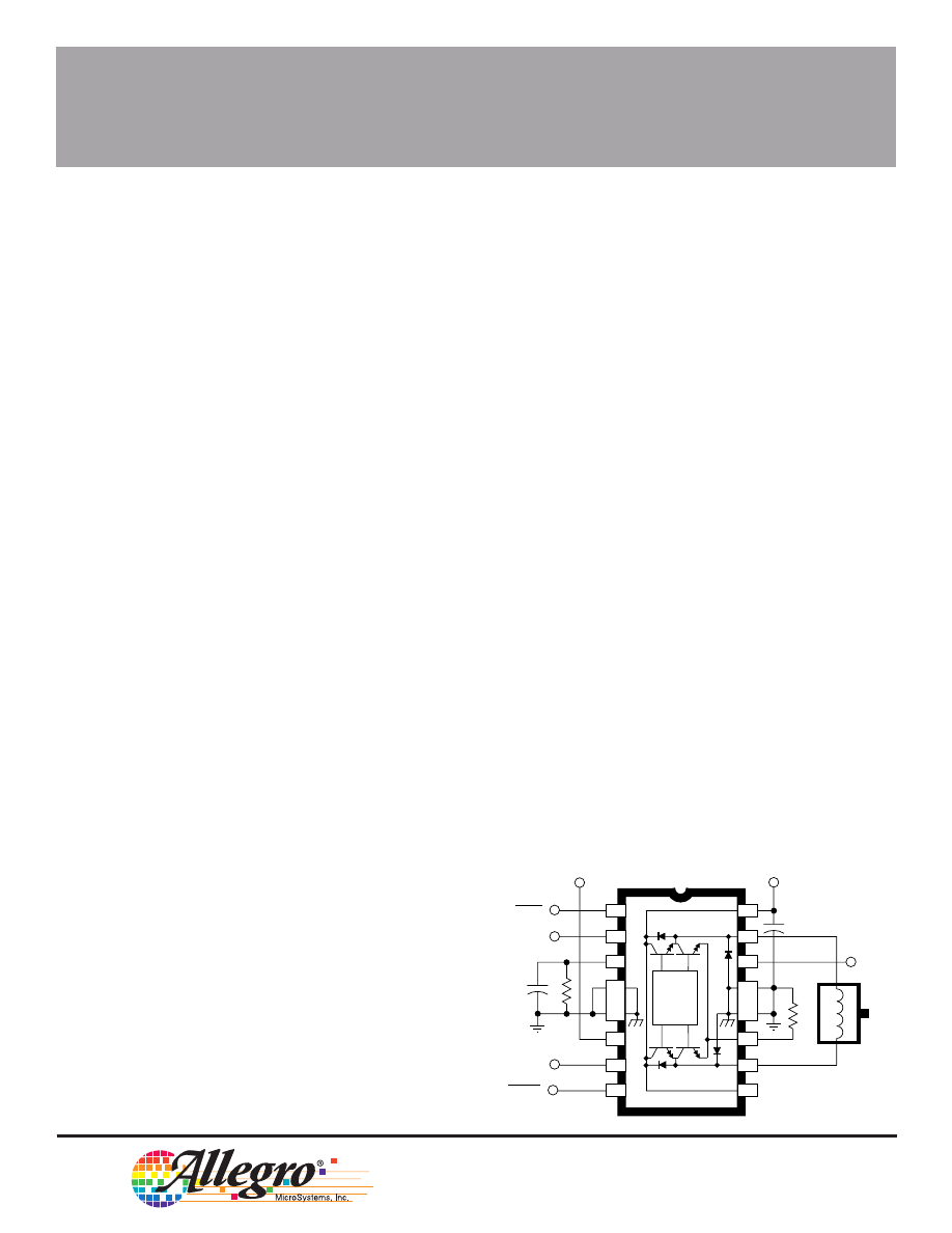
Part Number
Package
R
θ
JA
R
θ
JT
A3953SB
16-Pin DIP
43
°
C/W
6
°
C/W
A3953SLB
16-Lead SOIC
67
°
C/W
6
°
C/W
FULL-BRIDGE PWM MOTOR DRIVER
Always order by complete part number:
1
2
3
14
4
5
6
7
8
9
10
11
12
13
15
16
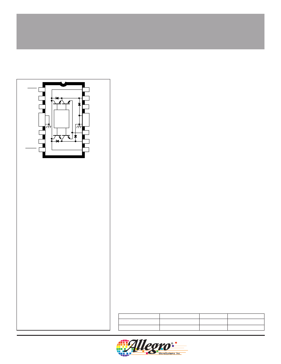
MODE
GROUND
GROUND
LOGIC
SUPPLY
PHASE
GROUND
GROUND
RC
SENSE
LOAD
SUPPLY
Dwg. PP-056
BRAKE
REF
LOAD
SUPPLY
V
CC
OUTB
OUTA
V
BB
V
BB
LOGIC
ENABLE
Note the A3953SB (DIP) and the A3953SLB
(SOIC) are electrically identical and share a
common terminal number assignment.
ABSOLUTE MAXIMUM RATINGS
Load Supply Voltage, V
BB
. . . . . . . . . . 50 V
Output Current, I
OUT
(Continuous) . . . . . . . . . . . . . .
±
1.3 A*
Logic Supply Voltage, V
CC
. . . . . . . . . 7.0 V
Logic/Reference Input Voltage Range,
V
IN
. . . . . . . . . . . -0.3 V to V
CC
+ 0.3 V
Sense Voltage, V
SENSE
(V
CC
= 5.0 V) . . . . . . . . . . . . . . . . 1.0 V
(V
CC
= 3.3 V) . . . . . . . . . . . . . . . . 0.4 V
Package Power Dissipation,
P
D
. . . . . . . . . . . . . . . . . . . . See Graph
Operating Temperature Range,
T
A
. . . . . . . . . . . . . . . . . -20˚C to +85˚C
Junction Temperature, T
J
. . . . . . . +150˚C†
Storage Temperature Range,
T
S
. . . . . . . . . . . . . . . . -55˚C to +150˚C
* Output current rating may be limited by duty
cycle, ambient temperature, and heat sinking.
Under any set of conditions, do not exceed the
specified current rating or a junction temperature
of 150˚C.
† Fault conditions that produce excessive junction
temperature will activate the device’s thermal
shutdown circuitry. These conditions can be
tolerated but should be avoided.
Designed for bidirectional pulse-width modulated (PWM) current
control of inductive loads, the A3953S— is capable of continuous
output currents to
±
1.3 A and operating voltages to 50 V. Internal fixed
off-time PWM current-control circuitry can be used to regulate the
maximum load current to a desired value. The peak load current limit
is set by the user’s selection of an input reference voltage and external
sensing resistor. The fixed off-time pulse duration is set by a user-
selected external RC timing network. Internal circuit protection includes
thermal shutdown with hysteresis, transient-suppression diodes, and
crossover current protection. Special power-up sequencing is not
required.
With the ENABLE input held low, the PHASE input controls load
current polarity by selecting the appropriate source and sink driver
pair. The MODE input determines whether the PWM current-control
circuitry operates in a slow current-decay mode (only the selected
source driver switching) or in a fast current-decay mode (selected
source and sink switching). A user-selectable blanking window
prevents false triggering of the PWM current-control circuitry. With the
ENABLE input held high, all output drivers are disabled. A sleep mode
is provided to reduce power consumption.
When a logic low is applied to the BRAKE input, the braking
function is enabled. This overrides ENABLE and PHASE to turn OFF
both source drivers and turn ON both sink drivers. The brake function
can be used to dynamically brake brush dc motors.
The A3953S— is supplied in a choice of two power packages; a
16-pin dual-in-line plastic package with copper heat-sink tabs, and a
16-lead plastic SOIC with copper heat-sink tabs. For both package
styles, the power tab is at ground potential and needs no electrical
isolation.
FEATURES
■
±
1.3 A Continuous Output Current
■
50 V Output Voltage Rating
■
3 V to 5.5 V Logic Supply Voltage
■
Internal PWM Current Control
■
Saturated Sink Drivers (Below 1 A)
■
Fast and Slow Current-Decay Modes
■
Automotive Capable
■
Sleep (Low Current
Consumption) Mode
■
Internal Transient-
Suppression Diodes
■
Internal Thermal-
Shutdown Circuitry
■
Crossover-Current
and UVLO Protection
Data Sheet
29319.8*
3953
3953
FULL-BRIDGE
PWM MOTOR DRIVER
115 Northeast Cutoff, Box 15036
Worcester, Massachusetts 01615-0036 (508) 853-5000
X = Irrelevant
FUNCTIONAL BLOCK DIAGRAM
V
BB
RC
V
CC
LOGIC
SUPPLY
LOAD
SUPPLY
9
PHASE
UVLO
& TSD
R S
Dwg. FP-036-2A
MODE
REF
OUT
A
OUT
B
ENABLE
SENSE
–
+
BRAKE
INPUT LOGIC
GROUND
Q
R
S
PWM LATCH
V
CC
+ –
BLANKING
SLEEP &
STANDBY MODES
VTH
R T
C T
1
2
3
6
7
8
10
11
14
15
4
GROUND
12
LOAD
SUPPLY
16
5
13
TRUTH TABLE
BRAKE
ENABLE
PHASE
MODE
OUT
A
OUT
B
DESCRIPTION
H
H
X
H
Off
Off
Sleep Mode
H
H
X
L
Off
Off
Standby
H
L
H
H
H
L
Forward, Fast Current-Decay Mode
H
L
H
L
H
L
Forward, Slow Current-Decay Mode
H
L
L
H
L
H
Reverse, Fast Current-Decay Mode
H
L
L
L
L
H
Reverse, Slow Current-Decay Mode
L
X
X
H
L
L
Brake, Fast Current-Decay Mode
L
X
X
L
L
L
Brake, No Current Control
Copyright © 1995, 1996 Allegro MicroSystems, Inc.

3953
FULL-BRIDGE
PWM MOTOR DRIVER
50
75
100
125
150
5
1
0
ALLOWABLE PACKAGE POWER DISSIPATION IN WATTS
TEMPERATURE IN
°
C
4
3
2
25
Dwg. GP-049-2A
R = 6.0
°
C/W
θ
JT
SUFFIX 'B', R = 43
°
C/W
θ
JA
SUFFIX 'LB', R = 63
°
C/W
θ
JA
ELECTRICAL CHARACTERISTICS at T
J
= 25˚C, V
BB
= 5 V to 50 V, V
CC
= 3.0 V to 5.5 V
(unless otherwise noted.)
Limits
Characteristic
Symbol
Test Conditions
Min.
Typ.
Max.
Units
Load Supply Voltage Range
V
BB
Operating, I
OUT
=
±
1.3 A, L = 3 mH
V
CC
—
50
V
Output Leakage Current
I
CEX
V
OUT
= V
BB
—
<1.0
50
µ
A
V
OUT
= 0 V
—
<-1.0
-50
µ
A
Sense Current Offset
I
SO
I
SENSE
- I
OUT1
, I
OUT
= 850 mA,
22
33
38
mA
V
SENSE
= 0 V, V
CC
= 5 V
Output Saturation Voltage
V
CE(SAT)
V
SENSE
= 0.4 V, V
CC
= 3.0 V:
BRAKE = H
Source Driver, I
OUT
= -0.85 A
—
1.0
1.1
V
(Forward/Reverse Mode)
Source Driver, I
OUT
= -1.3 A
—
1.7
1.9
V
Sink Driver, I
OUT
= 0.85 A
—
0.4
0.5
V
Sink Driver, I
OUT
= 1.3 A
—
1.1
1.3
V
Output Saturation Voltage
V
CE(SAT)
V
SENSE
= 0.4 V, V
CC
= 3.0 V:
BRAKE = L
Sink Driver, I
OUT
= 0.85 A
—
1.0
1.2
V
(Brake Mode)
Sink Driver, I
OUT
= 1.3 A
—
1.3
1.5
V
Clamp Diode Forward Voltage
V
F
I
F
= 0.85 A
—
1.2
1.4
V
(Sink or Source)
I
F
= 1.3 A
—
1.4
1.6
V
Continued next page…
Power Outputs

3953
FULL-BRIDGE
PWM MOTOR DRIVER
115 Northeast Cutoff, Box 15036
Worcester, Massachusetts 01615-0036 (508) 853-5000
PWM RC Fixed Off-time
t
OFF RC
C
T
= 680 pF, R
T
= 30 k
Ω
, V
CC
= 3.3 V
18.3
20.4
22.5
µ
s
PWM Turn-Off Time
t
PWM(OFF)
Comparator Trip to Source OFF,
—
1.0
1.5
µ
s
I
OUT
= 25 mA
Comparator Trip to Source OFF,
—
1.8
2.6
µ
s
I
OUT
= 1.3 A
PWM Turn-On Time
t
PWM(ON)
I
RC
Charge ON to Source ON,
—
0.4
0.7
µ
s
I
OUT
= 25 mA
I
RC
Charge ON to Source ON,
—
0.55
0.85
µ
s
I
OUT
= 1.3 A
PWM Minimum On Time
t
ON(min)
V
CC
= 3.3 V, R
T
≥
12 k
Ω
, C
T
= 680 pF
0.8
1.4
1.9
µ
s
V
CC
= 5.0 V, R
T
≥
12 k
Ω
, C
T
= 470 pF
0.8
1.6
2.0
µ
s
Propagation Delay Times
t
pd
I
OUT
=
±
1.3 A, 50% to 90%:
ENABLE ON to Source ON
—
1.0
—
µ
s
ENABLE OFF to Source OFF
—
1.0
—
µ
s
ENABLE ON to Sink ON
—
1.0
—
µ
s
ENABLE OFF to Sink OFF (MODE = L)
—
0.8
—
µ
s
PHASE Change to Sink ON
—
2.4
—
µ
s
PHASE Change to Sink OFF
—
0.8
—
µ
s
PHASE Change to Source ON
—
2.0
—
µ
s
PHASE Change to Source OFF
—
1.7
—
µ
s
Crossover Dead Time
t
CODT
1 k
Ω
Load to 25 V, V
BB
= 50 V
0.3
1.5
3.0
µ
s
Maximum PWM Frequency
f
PWM(max)
I
OUT
= 1.3 A
70
—
—
kHz
ELECTRICAL CHARACTERISTICS at T
J
= 25˚C, V
BB
= 5 V to 50 V, V
CC
= 3.0 V to 5.5 V
(unless otherwise noted.)
Limits
Characteristic
Symbol
Test Conditions
Min.
Typ.
Max.
Units
AC Timing
Continued next page…

3953
FULL-BRIDGE
PWM MOTOR DRIVER
ELECTRICAL CHARACTERISTICS at T
J
= 25˚C, V
BB
= 5 V to 50 V, V
CC
= 3.0 V to 5.5 V
(unless otherwise noted. )
Limits
Characteristic
Symbol
Test Conditions
Min.
Typ.
Max.
Units
Control Circuitry
Thermal Shutdown Temp.
T
J
—
165
—
°
C
Thermal Shutdown Hysteresis
∆
T
J
—
8.0
—
°
C
UVLO Enable Threshold
2.5
2.75
3.0
V
UVLO Hysteresis
0.12
0.17
0.25
V
Logic Supply Current
I
CC(ON)
V
ENABLE
= 0.8 V, V
BRAKE
= 2.0 V
—
42
50
mA
I
CC(OFF)
V
ENABLE
= 2.0 V, V
MODE
= 0.8 V
—
12
15
mA
I
CC(Brake)
V
BRAKE
= 0.8 V
—
42
50
mA
I
CC(Sleep)
V
ENABLE
= V
MODE
= V
BRAKE
= 2.0 V
—
500
800
µ
A
Motor Supply Current
I
BB(ON)
V
ENABLE
= 0.8 V
—
2.5
4.0
mA
(No Load)
I
BB(OFF)
V
ENABLE
= 2.0 V, V
MODE
= 0.8 V
—
1.0
50
µ
A
I
BB(Brake)
V
BRAKE
= 0.8 V
—
1.0
50
µ
A
I
BB(Sleep)
V
ENABLE
= V
MODE
= 2.0 V
—
1.0
50
µ
A
Logic Supply Voltage Range
V
CC
Operating
3.0
5.0
5.5
V
Logic Input Voltage
V
IN(1)
2.0
—
—
V
V
IN(0)
—
—
0.8
V
Logic Input Current
I
IN(1)
V
IN
= 2.0 V
—
<1.0
20
µ
A
I
IN(0)
V
IN
= 0.8 V
—
<-2.0
-200
µ
A
V
SENSE
Voltage Range
V
SENSE(3.3)
V
CC
= 3.0 V to 3.6 V
0
—
0.4
V
V
SENSE(5.0)
V
CC
= 4.5 V to 5.5 V
0
—
1.0
V
Reference Input Current
I
REF
V
REF
= 0 V to 1 V
—
—
±
5.0
µ
A
Comparator Input Offset Volt.
V
IO
V
REF
= 0 V
—
±
2.0
±
5.0
mV
3953
FULL-BRIDGE
PWM MOTOR DRIVER
115 Northeast Cutoff, Box 15036
Worcester, Massachusetts 01615-0036 (508) 853-5000
FUNCTIONAL DESCRIPTION
Internal PWM Current Control During Forward and
Reverse Operation. The A3953S— contains a fixed off-
time pulse-width modulated (PWM) current-control circuit
that can be used to limit the load current to a desired
value. The peak value of the current limiting (I
TRIP
) is set
by the selection of an external current sensing resistor
(R
S
) and reference input voltage (V
REF
). The internal
circuitry compares the voltage across the external sense
resistor to the voltage on the reference input terminal
(REF) resulting in a transconductance function approxi-
mated by:
where I
SO
is the offset due to base drive current.
In forward or reverse mode the current-control cir-
cuitry limits the load current as follows: when the load
current reaches I
TRIP
, the comparator resets a latch that
turns off the selected source driver or selected sink and
source driver pair depending on whether the device is
operating in slow or fast current-decay mode, respec-
tively.
In slow current-decay mode, the selected source
driver is disabled; the load inductance causes the current
to recirculate through the sink driver and ground clamp
diode. In fast current-decay mode, the selected sink and
source driver pair are disabled; the load inductance
causes the current to flow from ground to the load supply
via the ground clamp and flyback diodes.
The user selects an external resistor (R
T
) and capaci-
tor (C
T
) to determine the time period (t
OFF
= R
T
•C
T
) during
which the drivers remain disabled (see “RC Fixed Off-
time” below). At the end of the RC interval, the drivers are
enabled allowing the load current to increase again. The
PWM cycle repeats, maintaining the peak load current at
the desired value (see figure 2).
Figure 2
Fast and Slow Current-Decay Waveforms
INTERNAL PWM CURRENT CONTROL
DURING BRAKE-MODE OPERATION
Brake Operation - MODE Input High. The brake circuit
turns OFF both source drivers and turns ON both sink
drivers. For dc motor applications, this has the effect of
shorting the motor’s back-EMF voltage resulting in current
flow that dynamically brakes the motor. If the back-EMF
voltage is large, and there is no PWM current limiting, the
load current can increase to a value that approaches that
of a locked rotor condition. To limit the current, when the
I
TRIP
level is reached, the PWM circuit disables the
conducting sink drivers. The energy stored in the motor’s
inductance is discharged into the load supply causing the
motor current to decay.
As in the case of forward/reverse operation, the
drivers are enabled after a time given by t
OFF
= R
T
•C
T
(see
“RC Fixed Off-time” below). Depending on the back-EMF
voltage (proportional to the motor’s decreasing speed),
the load current again may increase to I
TRIP
. If so, the
PWM cycle will repeat, limiting the peak load current to
the desired value.
ENABLE
MODE
LOAD
CURRENT
RC
I
TRIP
Dwg. WP-015-1
RC
V
REF
R
S
I
TRIP
≈
- I
SO
Dwg. EP-006-13A
R S
BB
V
DRIVE CURRENT
RECIRCULATION (SLOW-DECAY MODE)
RECIRCULATION (FAST-DECAY MODE)
Figure 1 — Load-Current Paths

3953
FULL-BRIDGE
PWM MOTOR DRIVER
During braking, when the MODE input is high, the
peak current limit can be approximated by:
CAUTION: Because the kinetic energy stored in the motor
and load inertia is being converted into current, which
charges the V
BB
supply bulk capacitance (power supply
output and decoupling capacitance), care must be taken
to ensure the capacitance is sufficient to absorb the
energy without exceeding the voltage rating of any
devices connected to the motor supply.
Brake Operation - MODE Input Low. During braking,
with the MODE input low, the internal current-control
circuitry is disabled. Therefore, care should be taken to
ensure that the motor’s current does not exceed the
ratings of the device. The braking current can be mea-
sured by using an oscilloscope with a current probe
connected to one of the motor’s leads, or if the back-EMF
voltage of the motor is known, approximated by:
RC Fixed Off-Time. The internal PWM current-control
circuitry uses a one shot to control the time the driver(s)
remain(s) off. The one-shot time, t
OFF
(fixed off-time), is
determined by the selection of an external resistor (R
T
)
and capacitor (C
T
) connected in parallel from the RC
timing terminal to ground. The fixed off-time, over a range
of values of C
T
= 470 pF to 1500 pF and R
T
= 12 k
Ω
to
100 k
Ω
, is approximated by:
t
OFF
≈
R
T
• C
T
The operation of the circuit is as follows: when the
PWM latch is reset by the current comparator, the voltage
on the RC terminal will begin to decay from approximately
0.60 V
CC
. When the voltage on the RC terminal reaches
approximately 0.22 V
CC
, the PWM latch is set, thereby
enabling the driver(s).
RC Blanking. In addition to determining the fixed off-time
of the PWM control circuit, the C
T
component sets the
comparator blanking time. This function blanks the output
of the comparator when the outputs are switched by the
internal current-control circuitry (or by the PHASE,
BRAKE, or ENABLE inputs). The comparator output is
blanked to prevent false over-current detections due to
reverse recovery currents of the clamp diodes, and/or
switching transients related to distributed capacitance in
the load.
During internal PWM operation, at the end of the t
OFF
time, the comparator’s output is blanked and C
T
begins to
be charged from approximately 0.22 V
CC
by an internal
current source of approximately 1 mA. The comparator
output remains blanked until the voltage on C
T
reaches
approximately 0.60 V
CC
.
When a transition of the PHASE input occurs, C
T
is
discharged to near ground during the crossover delay
time (the crossover delay time is present to prevent
simultaneous conduction of the source and sink drivers).
After the crossover delay, C
T
is charged by an internal
current source of approximately 1 mA. The comparator
output remains blanked until the voltage on C
T
reaches
approximately 0.60 V
CC
.
When the device is disabled, via the ENABLE input,
C
T
is discharged to near ground. When the device is re-
enabled, C
T
is charged by an internal current source of
approximately 1 mA. The comparator output remains
blanked until the voltage on C
T
reaches approximately
0.60 V
CC
.
For 3.3 V operation, the minimum recommended
value for C
T
is 680 pF
±
5 %. For 5.0 V operation, the
minimum recommended value for C
T
is 470 pF
±
5%.
These values ensure that the blanking time is sufficient to
avoid false trips of the comparator under normal operating
conditions. For optimal regulation of the load current, the
above values for C
T
are recommended and the value of
R
T
can be sized to determine t
OFF
. For more information
regarding load current regulation, see below.
V
REF
R
S
I
TRIP BRAKE MH
≈
V
BEMF
– 1V
R
LOAD
I
PEAK BRAKE ML
≈

3953
FULL-BRIDGE
PWM MOTOR DRIVER
115 Northeast Cutoff, Box 15036
Worcester, Massachusetts 01615-0036 (508) 853-5000
LOAD CURRENT REGULATION WITH
INTERNAL PWM
CURRENT-CONTROL CIRCUITRY
When the device is operating in slow current-decay
mode, there is a limit to the lowest level that the PWM
current-control circuitry can regulate load current. The
limitation is the minimum duty cycle, which is a function of
the user-selected value of t
OFF
and the minimum on-time
pulse t
ON(min)
max that occurs each time the PWM latch is
reset. If the motor is not rotating (as in the case of a
stepper motor in hold/detent mode, a brush dc motor when
stalled, or at startup), the worst case value of current
regulation can be approximated by:
where t
OFF
= R
T
• C
T
, R
LOAD
is the series resistance of the
load, V
BB
is the motor supply voltage and t
ON(min)
max
is
specified in the electrical characteristics table. When the
motor is rotating, the back EMF generated will influence
the above relationship. For brush dc motor applications,
the current regulation is improved. For stepper motor
applications, when the motor is rotating, the effect is more
complex. A discussion of this subject is included in the
section on stepper motors below.
The following procedure can be used to evaluate the
worst-case slow current-decay internal PWM load current
regulation in the system:
Set V
REF
to 0 volts. With the load connected and the
PWM current control operating in slow current-decay
mode, use an oscilloscope to measure the time the output
is low (sink ON) for the output that is chopping. This is
the typical minimum ON time (t
ON(min)
typ) for the device.
The C
T
then should be increased until the measured value
of t
ON(min)
is equal to t
ON(min)
max as specified in the
electrical characteristics table. When the new value of C
T
has been set, the value of R
T
should be decreased so the
value for t
OFF
= R
T
• C
T
(with the artificially increased value
of C
T
) is equal to the nominal design value. The worst-
case load-current regulation then can be measured in the
system under operating conditions.
PWM of the PHASE and ENABLE Inputs. The PHASE
and ENABLE inputs can be pulse-width modulated to
regulate load current. Typical propagation delays from
the PHASE and ENABLE inputs to transitions of the
power outputs are specified in the electrical characteris-
tics table. If the internal PWM current control is used, the
comparator blanking function is active during phase and
enable transitions. This eliminates false tripping of the
over-current comparator caused by switching transients
(see “RC Blanking” above).
Enable PWM. With the MODE input low, toggling the
ENABLE input turns ON and OFF the selected source and
sink drivers. The corresponding pair of flyback and
ground-clamp diodes conduct after the drivers are
disabled, resulting in fast current decay. When
the device is enabled the internal current-control
circuitry will be active and can be used to limit the
load current in a slow current-decay mode.
For applications that PWM the ENABLE input and
desire the internal current-limiting circuit to function in the
fast decay mode, the ENABLE input signal should be
inverted and connected to the MODE input. This prevents
the device from being switched into sleep mode when the
ENABLE input is low.
Phase PWM. Toggling the PHASE terminal selects which
sink/source pair is enabled, producing a load current that
varies with the duty cycle and remains continuous at all
times. This can have added benefits in bidirectional brush
dc servo motor applications as the transfer function
between the duty cycle on the PHASE input and the
average voltage applied to the motor is more linear than in
the case of ENABLE PWM control (which produces a
discontinuous current at low current levels). For more
information see “DC Motor Applications” below.
Synchronous Fixed-Frequency PWM. The internal
PWM current-control circuitry of multiple A3953S—
devices can be synchronized by using the simple circuit
shown in figure 3. A 555 IC can be used to generate the
reset pulse/blanking signal (t
1
) for the device and the
period of the PWM cycle (t
2
). The value of t
1
should be a
minimum of 1.5 ms. When used in this configuration, the
R
T
and C
T
components should be omitted. The PHASE
and ENABLE inputs should not be PWM with this circuit
configuration due to the absence of a blanking function
synchronous with their transitions.
[(V
BB
– V
SAT(source+sink)
) • t
ON(min)
max] – (1.05(V
SAT(sink)
+ V
F
) • t
OFF
)
1.05 • (t
ON(min)
max + t
OFF
) • R
LOAD
I
AVE
≈
3953
FULL-BRIDGE
PWM MOTOR DRIVER
Figure 3
Synchronous Fixed-Frequency Control Circuit
Miscellaneous Information. A logic high applied to both
the ENABLE and MODE terminals puts the device into a
sleep mode to minimize current consumption when not in
use.
An internally generated dead time prevents crossover
currents that can occur when switching phase or braking.
Thermal protection circuitry turns OFF all drivers
should the junction temperature reach 165
°
C (typical).
This is intended only to protect the device from failures
due to excessive junction temperatures and should not
imply that output short circuits are permitted. The hyster-
esis of the thermal shutdown circuit is approximately
15
°
C.
APPLICATION NOTES
Current Sensing. The actual peak load current (I
PEAK
)
will be above the calculated value of I
TRIP
due to delays in
the turn off of the drivers. The amount of overshoot can
be approximated by:
where V
BB
is the motor supply voltage, V
BEMF
is the back-
EMF voltage of the load, R
LOAD
and L
LOAD
are the resis-
tance and inductance of the load respectively, and
t
PWM(OFF)
is specified in the electrical characteristics table.
The reference terminal has a maximum input bias
current of
±
5
µ
A. This current should be taken into
account when determining the impedance of the external
circuit that sets the reference voltage value.
To minimize current-sensing inaccuracies caused by
ground trace I • R drops, the current-sensing resistor
should have a separate return to the ground terminal of
the device. For low-value sense resistors, the I • R drops
in the printed wiring board can be significant and should
be taken into account. The use of sockets should be
avoided as their contact resistance can cause variations in
the effective value of R
S
.
Generally, larger values of R
S
reduce the aforemen-
tioned effects but can result in excessive heating and
power loss in the sense resistor. The selected value of R
S
should not cause the absolute maximum voltage rating of
1.0 V (0.4 V for V
CC
= 3.3 V operation), for the SENSE
terminal, to be exceeded.
The current-sensing comparator functions down to
ground allowing the device to be used in microstepping,
sinusoidal, and other varying current-profile applications.
Thermal Considerations. For reliable operation it is
recommended that the maximum junction temperature be
kept below 110
°
C to 125
°
C. The junction temperature can
be measured best by attaching a thermocouple to the
power tab/batwing of the device and measuring the tab
temperature, T
TAB
. The junction temperature can then be
approximated by using the formula:
T
J
≈
T
TAB
+ (I
LOAD
• 2 • V
F
• R
θ
JT
)
where V
F
may be chosen from the electrical specification
table for the given level of I
LOAD
. The value for R
θ
JT
is
given in the package thermal resistance table for the
appropriate package.
The power dissipation of the batwing packages can be
improved by 20% to 30% by adding a section of printed
circuit board copper (typically 6 to 18 square centimeters)
connected to the batwing terminals of the device.
The thermal performance in applications that run at
high load currents and/or high duty cycles can be im-
proved by adding external diodes in parallel with the
internal diodes. In internal PWM slow-decay applications,
only the two ground clamp diodes need be added. For
internal fast-decay PWM, or external PHASE or ENABLE
input PWM applications, all four external diodes should be
added for maximum junction temperature reduction.
PCB Layout. The load supply terminal, V
BB
, should be
decoupled with an electrolytic capacitor (>47
µ
F is recom-
Dwg. EP-060
100 k
Ω
20 k
Ω
1N4001
2N2222
V
CC
RC
1
RC
N
t
1
2
t
(V
BB
– [(I
TRIP
• R
LOAD
) + V
BEMF
]) • t
PWM(OFF)
L
LOAD
I
OS
≈
3953
FULL-BRIDGE
PWM MOTOR DRIVER
115 Northeast Cutoff, Box 15036
Worcester, Massachusetts 01615-0036 (508) 853-5000
mended) placed as close to the device as is physically
practical. To minimize the effect of system ground I • R
drops on the logic and reference input signals, the system
ground should have a low-resistance return to the motor
supply voltage.
See also “Current Sensing” and “Thermal Consider-
ations” above.
Fixed Off-Time Selection. With increasing values of t
OFF,
switching losses will decrease, low-level load-current
regulation will improve, EMI will be reduced, the PWM
frequency will decrease, and ripple current will increase.
The value of t
OFF
can be chosen for optimization of these
parameters. For applications where audible noise is a
concern, typical values of t
OFF
are chosen to be in the
range of 15 ms to 35 ms.
Stepper Motor Applications. The MODE terminal can
be used to optimize the performance of the device in
microstepping/sinusoidal stepper-motor drive applications.
When the load current is increasing, slow decay mode is
used to limit the switching losses in the device and iron
losses in the motor. This also improves the maximum rate
at which the load current can increase (as compared to
fast decay) due to the slow rate of decay during t
OFF
.
When the load current is decreasing, fast-decay mode is
used to regulate the load current to the desired level. This
prevents tailing of the current profile caused by the back-
EMF voltage of the stepper motor.
In stepper-motor applications applying a constant
current to the load, slow-decay mode PWM is typically
used to limit the switching losses in the device and iron
losses in the motor.
DC Motor Applications. In closed-loop systems, the
speed of a dc motor can be controlled by PWM of the
PHASE or ENABLE inputs, or by varying the reference
input voltage (REF). In digital systems (microprocessor
controlled), PWM of the PHASE or ENABLE input is used
typically thus avoiding the need to generate a variable
analog voltage reference. In this case, a dc voltage on the
REF input is used typically to limit the maximum load
current.
In dc servo applications, which require accurate
positioning at low or zero speed, PWM of the PHASE
input is selected typically. This simplifies the servo control
loop because the transfer function between the duty cycle
on the PHASE input and the average voltage applied to
the motor is more linear than in the case of ENABLE
PWM control (which produces a discontinuous current at
low current levels).
With bidirectional dc servo motors, the PHASE
terminal can be used for mechanical direction control.
Similar to when braking the motor dynamically, abrupt
changes in the direction of a rotating motor produces a
current generated by the back-EMF. The current gener-
ated will depend on the mode of operation. If the internal
current control circuitry is not being used, then the maxi-
mum load current generated can be approximated by
I
LOAD
= (V
BEMF
+ V
BB
)/R
LOAD
where V
BEMF
is proportional to
the motor’s speed. If the internal slow current-decay
control circuitry is used, then the maximum load current
generated can be approximated by I
LOAD
= V
BEMF
/R
LOAD
.
For both cases care must be taken to ensure that the
maximum ratings of the device are not exceeded. If the
internal fast current-decay control circuitry is used, then
the load current will regulate to a value given by:
I
LOAD
= V
REF
/R
S
.
CAUTION: In fast current-decay mode, when the direction
of the motor is changed abruptly, the kinetic energy stored
in the motor and load inertia will be converted into current
that charges the V
BB
supply bulk capacitance (power
supply output and decoupling capacitance). Care must be
taken to ensure that the capacitance is sufficient to absorb
the energy without exceeding the voltage rating of any
devices connected to the motor supply.
See also “Brake Operation” above.
Figure 4 — Typical Application
47
µ
F
+
1
2
3
4
5
6
7
8
9
10
11
12
13
14
15
16
V
CC
V
BB
V
BB
LOGIC
Dwg. EP-047-2A
30 k
Ω
0.5
Ω
V
BB
MODE
PHASE
ENABLE
BRAKE
470 pF
+5 V
REF
3953
FULL-BRIDGE
PWM MOTOR DRIVER
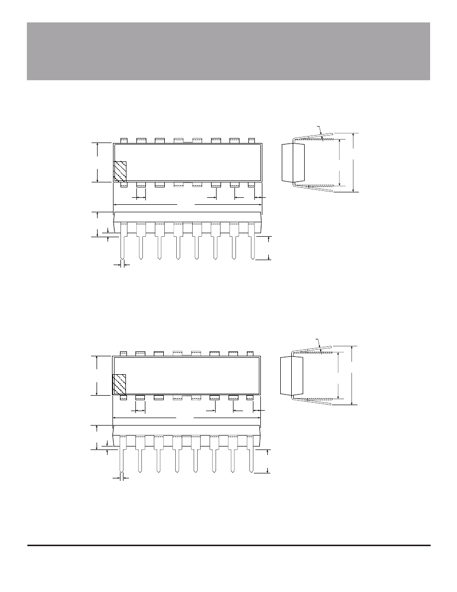
A3953SB
Dimensions in Inches
(controlling dimensions)
Dimensions in Millimeters
(for reference only)
NOTES: 1. Exact body and lead configuration at vendor’s option within limits shown.
2. Lead spacing tolerance is non-cumulative
3. Lead thickness is measured at seating plane or below.
4. Webbed lead frame. Leads 4, 5, 12, and 13 are internally one piece.
0.020
0.008
0.300
BSC
Dwg. MA-001-17A in
0.430
MAX
16
1
8
0.280
0.240
0.210
MAX
0.070
0.045
0.015
MIN
0.022
0.014
0.100
BSC
0.005
MIN
0.150
0.115
9
0.775
0.735
NOTE 4
0.508
0.204
7.62
BSC
Dwg. MA-001-17A mm
10.92
MAX
16
1
8
7.11
6.10
5.33
MAX
1.77
1.15
0.39
MIN
0.558
0.356
2.54
BSC
0.13
MIN
3.81
2.93
9
19.68
18.67
NOTE 4
3953
FULL-BRIDGE
PWM MOTOR DRIVER
115 Northeast Cutoff, Box 15036
Worcester, Massachusetts 01615-0036 (508) 853-5000
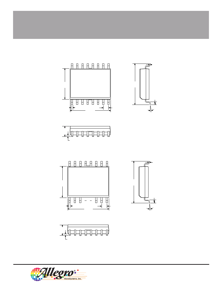
A3953SLB
Dimensions in Inches
(for reference only)
Dimensions in Millimeters
(controlling dimensions)
0
°
TO
8
°
1
2
3
0.2992
0.2914
0.4133
0.3977
0.419
0.394
0.020
0.013
0.0926
0.1043
0.0040
MIN.
0.0125
0.0091
0.050
0.016
Dwg. MA-008-17A in
0.050
BSC
16
9
0
°
TO
8
°
9
1
16
2
3
7.60
7.40
10.50
10.10
10.65
10.00
0.51
0.33
2.65
2.35
0.10
MIN.
0.32
0.23
1.27
0.40
Dwg. MA-008-17A mm
1.27
BSC
Allegro MicroSystems, Inc. reserves the right to make, from time to time, such departures from the
detail specifications as may be required to permit improvements in the design of its products.
Components made under military approvals will be in accordance with the approval requirements.
The information included herein is believed to be accurate and reliable. However, Allegro
MicroSystems, Inc. assumes no responsibility for its use; nor for any infringements of patents or other
rights of third parties which may result from its use.
NOTES: 1. Exact body and lead configuration at vendor’s
option within limits shown.
2. Lead spacing tolerance is non-cumulative
3. Webbed lead frame. Leads 4, 5, 12, and 13
are internally one piece.
Wyszukiwarka
Podobne podstrony:
3953
Program praktyk 2012 OK id 3953 Nieznany
3953
3953
3953
3953
3953
(3953) równania różniczkowe, Budownictwo 2, Budownictwo, Matematyka
(3953) równania różniczkowe
3953
więcej podobnych podstron