
AVR182: Zero Cross Detector
Features
•
Interrupt Driven
•
Modular C Source Code
•
Size Efficient Code
•
Accurate and Fast Detection
•
A Minimum of External Components
Introduction
One of the many issues with developing modern applications is to keep the spikes and
EMI at a minimum, especially when switching AC mains in and out. Most of today’s
new applications are controlled by one or more microcontrollers and this gives the
possibility to prevent this noise in a simple and cost efficient way.
Noise produced during switching is dependant on the amplitude of the AC sinus at the
actual switching point. To get this noise as low as possible the ideal switching would
be when the amplitude is 0 volt. The amplitude is crossing 0 volt at the sinus “zero
crossing”. Switching mains in and out at the zero crossing requires a way of detecting
when the next crossing will be and launching a switching action at the crossing. This
raises the need for a cost efficient way to detect the zero crossing. This application
note explains how to do that.
Zero cross detection can also be used for other purposes, such as frequency calcula-
tion and relative phase measuring.
8-bit
RISC
Microcontroller
Application
Note
Rev. 2508B–AVR–01/04
2
AVR182
2508B–AVR–01/04
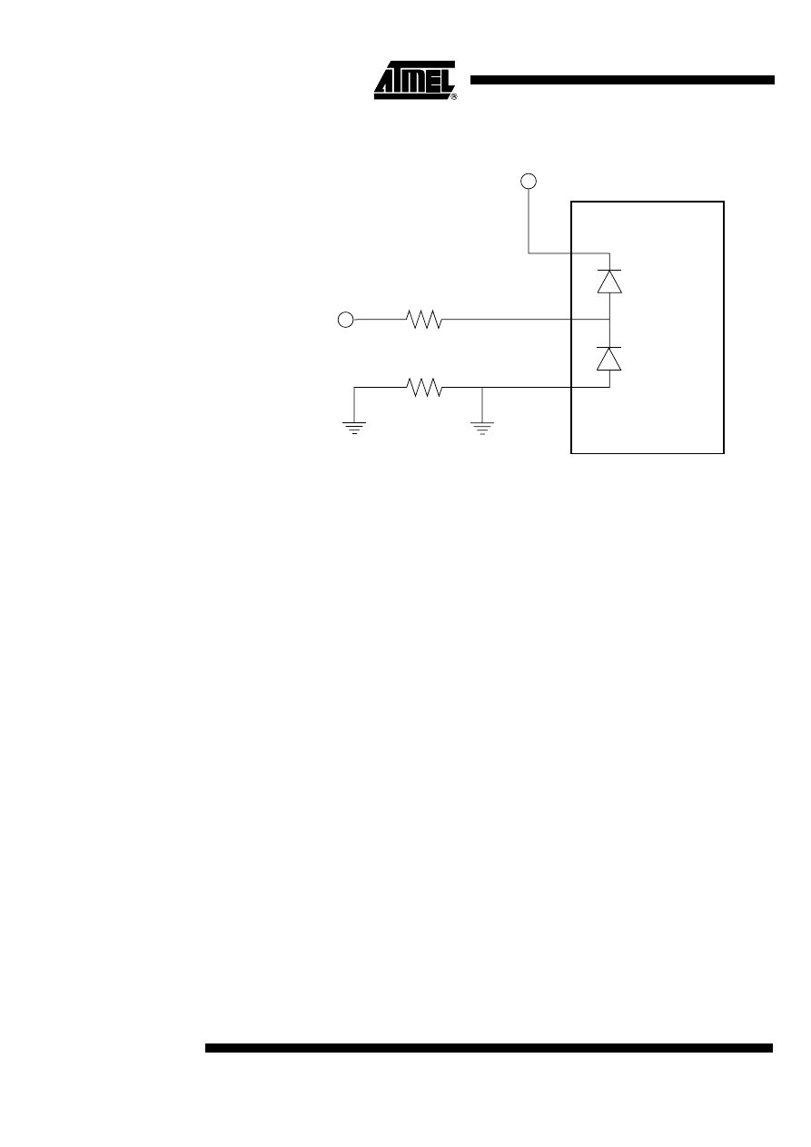
Figure 1. Zero Cross Detector Using AVR
®
Application Example
This application note shows the user how to implement a zero cross detector with a min-
imum of external components. It should be noted that this solution will not give any
galvanic isolation for the microcontroller against the AC mains. The zero cross sense
resistor can be a way for electronic noise to get into the system.
This will not be described in this application note. Please see “AVR040: EMC Design
Considerations” for further details about this.
The application uses ATmega16, but the code can be recompiled for any AVR device.
Hardware
To protect the device from voltages above V
CC
and below GND, the AVR has internal
clamping diodes on the I/O pins (see Figure 1). The diodes are connected from the pins
to V
CC
and GND and keep all input signals within the AVR’s operating voltage (see Fig-
ure 2). Any voltage higher than V
CC
+ 0.5V will be forced down to V
CC
+ 0.5V (0.5V is the
voltage drop over the diode) and any voltage below GND - 0.5V will be forced up to
GND - 0.5V.
By adding a large resistor in series, these diodes can be used to convert a high voltage
sinus signal down to a low voltage square wave signal, with amplitude within the AVR’s
operating voltage ± 0.5V. The diodes will thus clamp the high voltage signal down to the
AVR’s operating voltage.
Note that the series resistor and the pin input capacitance form an RC filter that will
introduce a small phase difference between the square wave and the AC mains signal.
The phase difference is insignificant in the current example, see “RC Filter and Delay
Between VCC/2 and the Actual Zero Cross” on page 7 for more details.
As the square wave signal is in phase with the AC mains, using the falling edge will tell
very accurately where the zero crossing happens. By using this signal the AVR can be
programmed to be a very accurate zero cross detector with a very small and interrupt-
driven code.
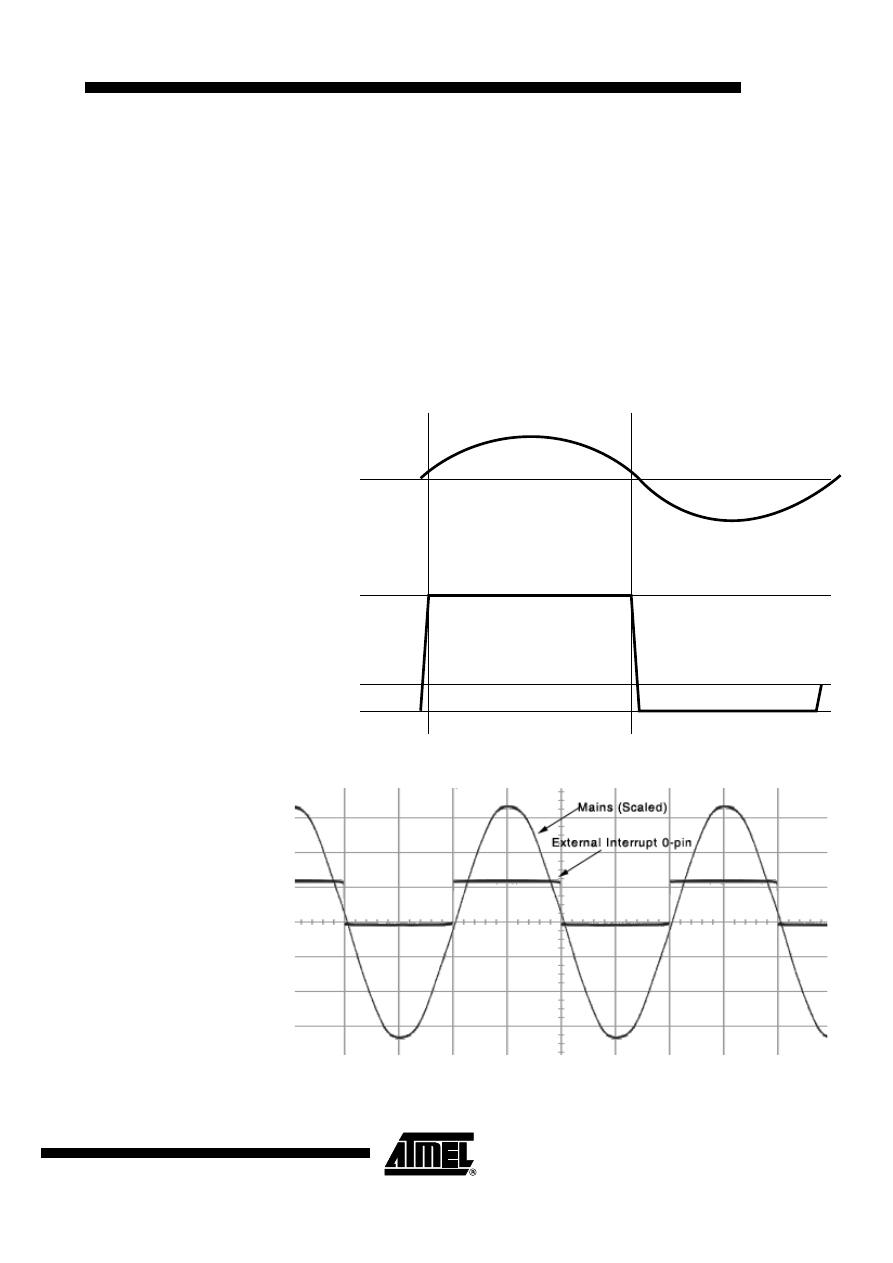
The square wave is the mains signal with its tops cut off and will have the same voltage
from V
CC
- 0.5V to V
CC
+ 0.5V as the mains signal (see Figure 2). When the square
Mains GND
GND
1M
1M
Mains
Serial Input Resistor
V
CC
VCC
PD2/EXT INT0
GND
ATmega163
AVR
3
AVR182
2508B–AVR–01/04
wave triggers the AVR’s falling edge interrupt at around V
CC
/2, the mains amplitude will
also be at V
CC
/2 and just before a zero crossing. If this is done on a falling edge the AVR
will get an interrupt just before the zero crossing and will have time to start a zero cross-
ing action at the actual crossing point. The interrupt will be triggered at around V
CC
/2, as
this is the middle of the AVR’s logical threshold voltage.
The signal is connected to the External Interrupt 0-pin which makes it possible to place
the zero cross detection routine in an interrupt routine and make the detection fully inter-
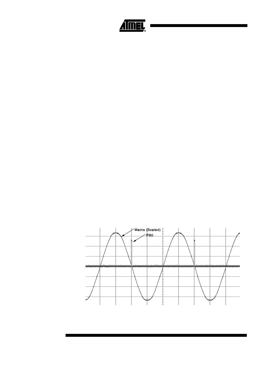
rupt driven. Figure 3 shows a oscilloscope screenshot of the actual input signal. Note
that the Mains signal is scaled and the rising edge of the external int 0-pin is the same
edge as for the Mains, because of the scaling, the Mains edge looks like it appears after
the external int 0 edge.
Figure 2. Square Wave Input Signal on External Interrupt 0-pin
Figure 3. Oscilloscope Screenshot of Square Wave Input on External Interrupt 0-pin
V
CC
+ 0.5V
V
CC
+ 0.5V
110 - 240 V AC
Mains
Mains GND
V
CC
+ 0.5V
Squarewave on
External Interrupt 0
AVR GND
GND - 0.5V
4
AVR182
2508B–AVR–01/04
The series input resistor is a 1 M
Ω
resistor. It is not recommended that the clamping
diodes are conducting more than maximum 1 mA and 1 M
Ω
will then allow a maximum
voltage of approximately 1,000V.
Any voltage higher than 1,000V would probably be spikes or surges. The clamping
diodes are able to handle spikes for a short period of time but not surges. The applica-
tion note will not go into how to protect against surges, but simply recommend
implementing protection against surges in the design.
Most resistors have an upper maximum voltage limit. Make sure that the resistors used
in the application can handle the highest possible AC mains voltage, including high volt-
age spikes.
For systems with lower mains voltages the resistor value can be changed, but in general
it should be able to sense 110 - 240V AC systems without any problems.
The 1 M
Ω
resistor in series to mains GND will ensure a correct ground potential for the
application.
Software
The external hardware and internal clamping diodes will make a square wave signal on
the AVR’s External Interrupt 0-pin. As described in the hardware section the square
wave will have the same frequency as the AC mains. The high period of the signal will
be when the AC mains amplitude is above V
CC
/2. This gives mains zero crossings very
close to the edges of the square wave. The rising edge of the square wave is slightly
after the crossing and the falling edge is slightly before the crossing.
As the falling edge of the square wave is just before a zero crossing, the falling edge
interrupt will occur so close to the actual crossing that it immediately can start the zero
crossing action.
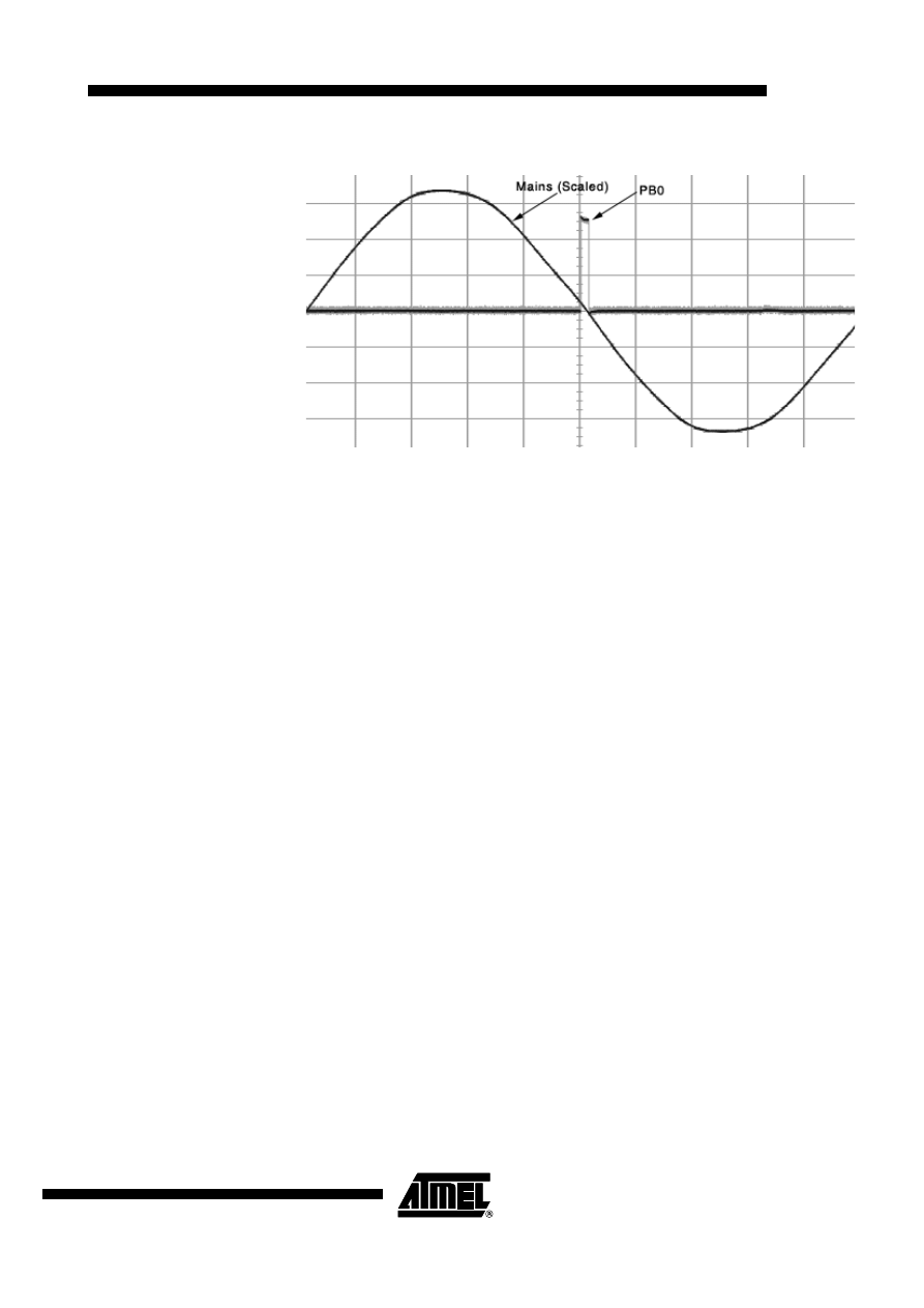
In this application example the zero crossing action will only be to set PB0 high for a
short period of time and then immediately start looking for the next falling edge zero
crossing. This makes it very easy to check if the zero crossing detection is correct or
not. Simply connect an oscilloscope probe to the mains and another to PB0. If the detec-
tion is correct this will show PB0 going high for a short period of time at each negative
edge zero crossing (See Figure 4 and Figure 5).
Figure 4. Screenshoot from Oscilloscope, Mains Input and PB0 Output
5
AVR182
2508B–AVR–01/04
Figure 5. Screenshot from Oscilloscope, Mains Input and PB0 Output
In a real application the disabling of external interrupt 0 before returning from the inter-
rupt routine will make a single detection. To detect a new zero crossing, simply enable
the falling edge interrupt again in the main program.
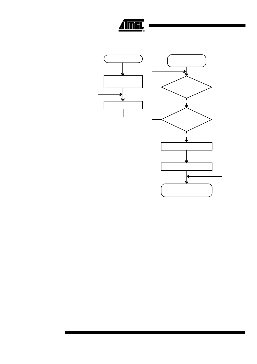
To make sure the interrupts are valid and not only products of spikes on the pin, there is
a filter implemented in the interrupt routine. The filter samples the level on the interrupt
line five times and compares the values to see if the value is stable. If the value is not
the same for all the samples, the event is discarded and the routine returns to the main
program waiting for a new interrupt (See Figure 6).
For more details about the software, please see the comments in the code.
6
AVR182
2508B–AVR–01/04
Figure 6. Software Flowchart for Main Program and External Interrupt 0 Handling
Routine
Main Program
Enable EXT INT0
(Falling Edge)
Eternal Loop
Start EXT INT0
Handler Routine
EXT INT0
Pin Low?
EXT INT0 Pin
Sampled Low
5 Times?
Set PB0 High
Set PB0 Low
End EXT INT0
Handler Routine
no
no
yes
yes

7
AVR182
2508B–AVR–01/04
Special
Considerations
Applying high voltages to microcontrollers increases the possibility of malfunction or
injury. It is advisable to follow a few special steps as any error can cause severe dam-
age to components, emulators or electric shock.
Emulators and Clamp
Diodes
The AVR family is set up with a complete system of emulators, but because of the
nature of the PODs of some of the emulators, they are not equipped with internal clamp-
ing diodes. ICE200 and ICE40/50 are the only emulators with clamping diodes. ICE10
and ICE30 do not contain clamping diodes. By adding external clamping diodes these
emulators will get the same input as the part.
To apply a high AC voltage to an emulator can cause severe damage on the equipment
and care should be exercised. It is recommended to use isolation transformers on the
mains and galvanic separated RS-232 communication to the PC.
RC Filter and Delay
Between V
CC
/2 and the
Actual Zero Cross
The series resistor and the input pin capacitance will form an RC filter, which will delay
the response compared to the actual zero crossing.
The 1 M
Ω
resistor together with the input capacitance on the AVR introduces a delay
that brings the detection very close to the actual crossing. For other AC voltages or
series resistors it is recommended to do a test with an oscilloscope to see how close the
detection is to the actual crossing. This makes it very easy to check if the zero crossing
detection is correct or not. Connect an oscilloscope probe to the mains and another to
PB0. A correct detection will show PB0 going high for a short period of time at each fall-
ing edge zero crossing (see Figure 4 and Figure 5).
If the detection is after the actual crossing, the next crossing should be targeted by add-
ing a delay to the action. The delay should be equal to the time left before the next
crossing
The series resistor can also be modified somewhat to make the detection closer but
note that the maximum current through the AVR’s clamping diode should not be higher
than 1 mA.
Ground must Be
Symmetrical
The mains ground must be symmetrical to the phases in the mains net. As the sensor is
only using one phase and ground, this is necessary to detect the actual zero crossing
according to the three phases in the mains net. If ground is not symmetrical it is not pos-
sible to know when the crossing is using only one phase. This can only be a problem in
delta shaped mains net. Most countries, except Norway and Albania, use star shaped
mains system and will not have this problem.
How to Calculate a Slow
Switch (Relay)
The typical use of a zero cross detector can be to control a mains relay. As relays have
a response time that will be larger than the delay from the zero cross sensing to the
actual crossing one technique can be to add a delay to the handling, i.e., sense the
crossing on falling edge and make the relay close on rising edge.
To do this, the response time of the relay and the frequency of the mains has to be
known. These values can either be known from the manufacturer, measured in a lab or
by the AVR itself.
The measurement can be implemented into the AVR software. By using the zero cross
detector it can easily sample the frequency of the signal and with few external compo-
nents it can also measure the relay response time. This will give a universal system that
can adapt to almost any AC mains frequency and relay response time. It will also con-
tinue being correct even if the relay response time or frequency will change over time.

Printed on recycled paper.
Disclaimer: Atmel Corporation makes no warranty for the use of its products, other than those expressly contained in the Company’s standard
warranty which is detailed in Atmel’s Terms and Conditions located on the Company’s web site. The Company assumes no responsibility for any
errors which may appear in this document, reserves the right to change devices or specifications detailed herein at any time without notice, and
does not make any commitment to update the information contained herein. No licenses to patents or other intellectual property of Atmel are
granted by the Company in connection with the sale of Atmel products, expressly or by implication. Atmel’s products are not authorized for use
as critical components in life support devices or systems.
Atmel Corporation
Atmel Operations
2325 Orchard Parkway
San Jose, CA 95131, USA
Tel: 1(408) 441-0311
Fax: 1(408) 487-2600
Regional Headquarters
Europe
Atmel Sarl
Route des Arsenaux 41
Case Postale 80
CH-1705 Fribourg
Switzerland
Tel: (41) 26-426-5555
Fax: (41) 26-426-5500
Asia
Room 1219
Chinachem Golden Plaza
77 Mody Road Tsimshatsui
East Kowloon
Hong Kong
Tel: (852) 2721-9778
Fax: (852) 2722-1369
Japan
9F, Tonetsu Shinkawa Bldg.
1-24-8 Shinkawa
Chuo-ku, Tokyo 104-0033
Japan
Tel: (81) 3-3523-3551
Fax: (81) 3-3523-7581
Memory
2325 Orchard Parkway
San Jose, CA 95131, USA
Tel: 1(408) 441-0311
Fax: 1(408) 436-4314
Microcontrollers
2325 Orchard Parkway
San Jose, CA 95131, USA
Tel: 1(408) 441-0311
Fax: 1(408) 436-4314
La Chantrerie
BP 70602
44306 Nantes Cedex 3, France
Tel: (33) 2-40-18-18-18
Fax: (33) 2-40-18-19-60
ASIC/ASSP/Smart Cards
Zone Industrielle
13106 Rousset Cedex, France
Tel: (33) 4-42-53-60-00
Fax: (33) 4-42-53-60-01
1150 East Cheyenne Mtn. Blvd.
Colorado Springs, CO 80906, USA
Tel: 1(719) 576-3300
Fax: 1(719) 540-1759
Scottish Enterprise Technology Park
Maxwell Building
East Kilbride G75 0QR, Scotland
Tel: (44) 1355-803-000
Fax: (44) 1355-242-743
RF/Automotive
Theresienstrasse 2
Postfach 3535
74025 Heilbronn, Germany
Tel: (49) 71-31-67-0
Fax: (49) 71-31-67-2340
1150 East Cheyenne Mtn. Blvd.
Colorado Springs, CO 80906, USA
Tel: 1(719) 576-3300
Fax: 1(719) 540-1759
Biometrics/Imaging/Hi-Rel MPU/
High Speed Converters/RF Datacom
Avenue de Rochepleine
BP 123
38521 Saint-Egreve Cedex, France
Tel: (33) 4-76-58-30-00
Fax: (33) 4-76-58-34-80
Literature Requests
www.atmel.com/literature
2508B–AVR–01/04
© Atmel Corporation 2003. All rights reserved. Atmel
®
and combinations thereof, AVR
®
, and AVR Studio
®
are the registered trademarks of
Atmel Corporation or its subsidiaries. Microsoft
®
, Windows
®
, Windows NT
®
, and Windows XP
®
are the registered trademarks of Microsoft Corpo-
ration. Other terms and product names may be the trademarks of others
Document Outline
Wyszukiwarka
Podobne podstrony:
AVR182 Zero Cross Detector pl i Nieznany (2)
AVR205 Zero Cross Detector en i Nieznany (2)
07 safety chain solution Zero speed detection
Collaborative Defense Against Zero Day and Polymorphic Worms Detection, Response and an Evaluation F
Efficient Content Based Detection of Zero Day Worms
SweetBait Zero Hour Worm Detection and Containment Using Honeypots
Budzik Versa wielkość karty kredytowej instrukcja EN
G2 4 PW EN wn Rys 01
Detector De Metales
Manual Acer TravelMate 2430 US EN
Ćwiczenie 01 EN DI
eci en
BVSOI 3 001 E en
A Biegus projektowanie konctrukcji stalowych wg PN EN 1993 1 1 cz 1
OAEB Staining to Detect Apoptosis
więcej podobnych podstron