
Nand Flash
DesignWare Memory Model
Reference
Included in the VCS Verification Library
and the DesignWare Library
September 10, 2005

Copyright Notice and Proprietary Information
Copyright
2004 Synopsys, Inc. All rights reserved. This software and documentation contain confidential and proprietary
information that is the property of Synopsys, Inc. No part of the software and documentation may be reproduced, transmitted, or
translated, in any form or by any means, electronic, mechanical, manual, optical, or otherwise, without prior written permission of
Synopsys, Inc., or as expressly provided by the license agreement.
Destination Control Statement
All technical data contained in this publication is subject to the export control laws of the United States of America.
Disclosure to nationals of other countries contrary to United States law is prohibited. It is the reader’s responsibility to
determine the applicable regulations and to comply with them.
Disclaimer
SYNOPSYS, INC., AND ITS LICENSORS MAKE NO WARRANTY OF ANY KIND, EXPRESS OR IMPLIED, WITH
REGARD TO THIS MATERIAL, INCLUDING, BUT NOT LIMITED TO, THE IMPLIED WARRANTIES OF
MERCHANTABILITY AND FITNESS FOR A PARTICULAR PURPOSE.
Registered Trademarks (®)
Synopsys, AMPS, Arcadia, C Level Design, C2HDL, C2V, C2VHDL, Calaveras Algorithm, CoCentric, COSSAP, CSim,
DelayMill, Design Compiler, DesignPower, DesignWare, Device Model Builder, Enterprise, EPIC, Formality, HSPICE,
Hypermodel, I, InSpecs, in-Sync, LEDA, MAST, Meta, Meta-Software, ModelAccess, ModelExpress, ModelTools,
PathBlazer, PathMill, Physical Compiler, PowerArc, PowerMill, PrimeTime, RailMill, Raphael, RapidScript, Saber,
SmartLogic, SNUG, SolvNet, Stream Driven Simulator, Superlog, System Compiler, TestBench Manager, Testify,
TetraMAX, TimeMill, TMA, VERA, and VeriasHDL are registered trademarks of Synopsys, Inc.
Trademarks (™)
Active Parasitics, AFGen, Apollo, Apollo II, Apollo-DPII, Apollo-GA, ApolloGAII, Astro, Astro-Rail, Astro-Xtalk, Aurora,
AvanTestchip, AvanWaves, BCView, Behavioral Compiler, BOA, BRT, Cedar, ChipPlanner, Circuit Analysis, Columbia,
Columbia-CE, Comet 3D, Cosmos, Cosmos SE, CosmosLE, Cosmos-Scope, Cyclelink, Davinci, DC Expert, DC
Expert Plus, DC Professional, DC Ultra, DC Ultra Plus, Design Advisor, Design Analyzer, DesignerHDL, DesignTime,
DFM-Workbench, DFT Compiler SoCBIST, Direct RTL, Direct Silicon Access, DW8051, DWPCI,
Dynamic-Macromodeling, Dynamic Model Switcher, ECL Compiler, ECO Compiler, EDAnavigator, Encore, Encore PQ,
Evaccess, ExpressModel, Floorplan Manager, Formal Model Checker, FormalVera, FoundryModel, FPGA Compiler II,
FPGA Express, Frame Compiler, Frameway, Gatran, HDL Advisor, HDL Compiler, Hercules, Hercules-Explorer,
Hercules-II, Hierarchical Optimization Technology, High Performance Option, HotPlace, HSPICE-Link, Integrator,
Interactive Waveform Viewer, iQBus, Jupiter, Jupiter-DP, JupiterXT, JupiterXT-ASIC, JVXtreme, Liberty,
Libra-Passport, Library Compiler, Libra-Visa, LRC, Mars, Mars-Rail, Mars-Xtalk, Medici, Metacapture, Metacircuit,
Metamanager, Metamixsim, Milkyway, ModelSource, Module Compiler, MS-3200, MS-3400, NanoSim, Nova Product
Family, Nova-ExploreRTL, Nova-Trans, Nova-VeriLint, Nova-VHDLlint, OpenVera, Optimum Silicon, Orion_ec,
Parasitic View, Passport, Planet, Planet-PL, Planet-RTL, Polaris, Polaris-CBS, Polaris-MT, Power Compiler,
PowerCODE, PowerGate, ProFPGA, Progen, Prospector, Proteus OPC, Protocol Compiler, PSMGen, Raphael-NES,
RoadRunner, RTL Analyzer, Saber Co-Simulation, Saber for IC Design, SaberDesigner, SaberGuide, SaberRT,
SaberScope, SaberSketch, Saturn, ScanBand, Schematic Compiler, Scirocco, Scirocco-i, Shadow Debugger, Silicon
Blueprint, Silicon Early Access, SinglePass-SoC, Smart Extraction, SmartLicense, SmartModel Library, Softwire,
Source-Level Design, Star, Star-DC, Star-Hspice, Star-HspiceLink, Star-MS, Star-MTB, Star-Power, Star-Rail, Star-RC,
Star-RCXT, Star-Sim, Star-Sim XT, Star-Time, Star-XP, SWIFT, Taurus, Taurus-Device, Taurus-Layout,
Taurus-Lithography, Taurus-OPC, Taurus-Process, Taurus-Topography, Taurus-Visual, Taurus-Workbench, Test
Compiler, TestGen, TetraMAX TenX, The Power in Semiconductors, TheHDL, TimeSlice, TimeTracker, Timing
Annotator, TopoPlace, TopoRoute, Trace-On-Demand, True-Hspice, TSUPREM-4, TymeWare, VCS, VCS Express,
VCSi, Venus, Verification Portal, VFormal, VHDL Compiler, VHDL System Simulator, VirSim, and VMC are trademarks
of Synopsys, Inc.
Service Marks (
SM
)
DesignSphere, SVP Café, and TAP-in are service marks of Synopsys, Inc.
SystemC is a trademark of the Open SystemC Initiative and is used under license.
All other product or company names may be trademarks of their respective owners.
Printed in the U.S.A.
2
Synopsys, Inc.
September 10, 2005
Nand Flash DesignWare Memory Model Reference

September 10, 2005
Synopsys, Inc.
3
Nand Flash DesignWare Memory Model Reference
Nand Flash Specifications
This chapter includes information for using Nand Flash DesignWare Memory Models.
DesignWare Memory Models support the following Nand Flash types:
●
Basic Nand Flash
●
AMD Nand Flash
●
Advanced Nand Flash
●
Multiplane Nand Flash
Nand Flash Chapter Contents
●
“Nand Flash Supported Features” on page 4
●
“Features Not Modeled” on page 6
●
“Modeling Assumptions” on page 6
❍
“X-Handling Strategy in Nand Flash” on page 7
❍
“Timings in Function-Only Models” on page 8
❍
“Model Configuration Strategy” on page 8
❍
“Modeling Implementations” on page 11
●
“Initializing a Memory Array and the DefaultData Attribute” on page 16

4
Synopsys, Inc.
September 10, 2005
Nand Flash DesignWare Memory Model Reference
Nand Flash Supported Features
DesignWare Memory Models support the following features of Nand Flash memory.
Basic Nand Flash
●
Page Program
●
Block Erase
●
Serial Page Read
●
Sequential Row Read
●
Copy Back Program
●
Double Page Program
●
Program/Erase protection using the Write Protect pin
●
Read Status command
●
Read ID command
●
Supported vendors: Samsung, Fujitsu
AMD Nand Flash
●
Page Program
●
Block Erase
●
Serial Page Read
●
Sequential Row Read
●
Block Erase suspend/resume
●
Program/Erase protection using the Write Protect pin
●
Read Status command
●
Read ID command
●
Supported vendor: AMD

September 10, 2005
Synopsys, Inc.
5
Nand Flash DesignWare Memory Model Reference
Advance Nand Flash
●
Page Program
●
Cache Program
●
Copy Back Program
●
Block Erase
●
Serial Page Read
●
Random Data Read
●
Random Data Write
●
Program/Erase protection using the Write Protect pin
●
Read Status command
●
Read ID command
●
Supported vendor: Samsung
Multiplane Nand Flash
●
Page Program
●
Multiplane Page Program
●
Copy Back Program
●
Multiplane Copy Back Program
●
Block Erase
●
Multiplane Block Erase
●
Serial Page Read
●
Sequential Row Read
●
Program/Erase protection using the Write Protect pin
●
Read Status, Read Multiplane Status commands
●
Read ID command
●
Supported vendor: Samsung

6
Synopsys, Inc.
September 10, 2005
Nand Flash DesignWare Memory Model Reference
Features Not Modeled
●
The transition time tr (from BUSY to READY) depends on the pull-up resister
connected to the R/B# pin. Time tr is not modeled, and is assumed to be 0 ns.
●
Advanced Nand Flash uses an internal voltage detector during power-on to enable
the auto-page read function when Vcc reaches approximately 1.8V. The Power-On
Auto Read pin controls activation of the auto-page read function.
In the model, the auto-page read function is enabled by sampling the Power-On
Auto Read pin at 0 ns simulation time.
Modeling Assumptions
●
If an incomplete number of address cycles is performed, the model ignores those
cycles, and refers to the previous contents of the address register. The current
operation continues.
●
If read cycles are performed after aborting Read Busy (by deasserting Chip Enable
during Read Busy), the model drives X (Unknown) on the data bus, since the
contents of the data register will have been modified to an unknown extent.
●
If read cycles are performed beyond permissible page/block boundaries (specific to
each model), the model drives the contents of the last valid read.
●
Basic Nand Flash requires that the Spare Area Enable pin be stable during Program
and Read operations. Any event on the pin during either of these operations is
ignored, and the device continues its action according to the status the pin had at the
start of the operation.
●
If an illegal command sequence or a prohibited command is performed, the model
will be forced into the Illegal state, and a Reset command is necessary to continue.
●
If X or Z values are detected on an I/O bus during a command or an Address Write,
the model ignores the command or address.
●
The address counter does not increment if the Read Enable pin is toggled during
Read Busy.
●
The model has no invalid/bad blocks.
September 10, 2005
Synopsys, Inc.
7
Nand Flash DesignWare Memory Model Reference
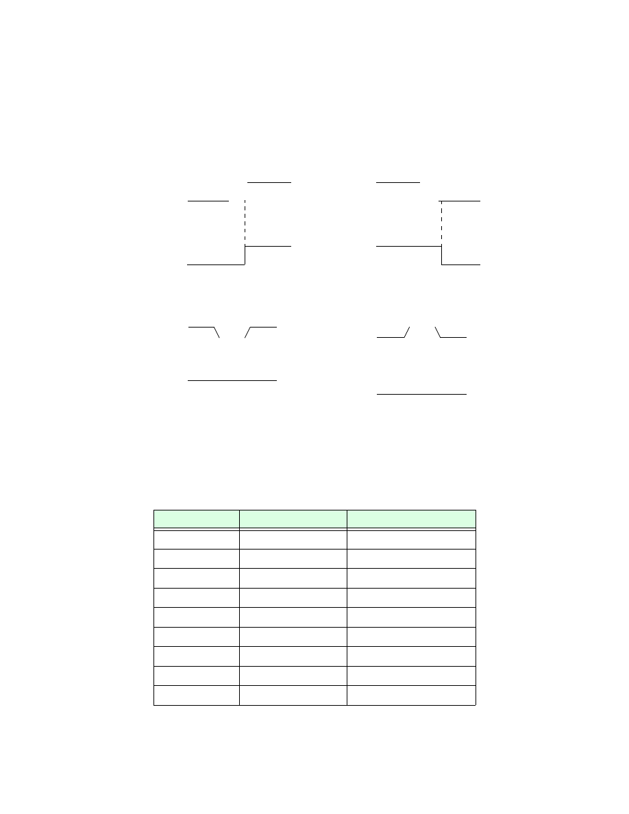
X-Handling Strategy in Nand Flash
The model can perform two types of X-handling, as defined below.
Type 1 Filtering
Type 2 Filtering
In Type 2 filtering, if an X is detected on any pin, the pin’s deasserted value is returned,
and a warning is issued as appropriate.
Table 1: Filtering Definitions
Pin/Bus
Situation/State
Assumed Operation
CE
—
Type 2 X-filtering.
WE
CE asserted.
Type 1 X-filtering.
RE
CE asserted.
Type 1 X-filtering.
CLE
CE asserted.
Type 1 X-filtering.
ALE
CE asserted.
Type 1 X-filtering.
SE
—
Type 1 X-filtering.
WP
—
Type 1 X-filtering.
Data bus
—
No X-filtering.
PRE(1)
a
a. This pin is present only on Advanced Nand Flash.
—
Type 1 X-filtering.
Transition:
1
X
0
Filtered:
1
0
XXX
Transition:
1
X
0
Filtered:
1
0
X
X
X
Transition:
1
x
Assumed:
1
0
XXX
Transition:
x
0
Assumed:
1
0
XXX

8
Synopsys, Inc.
September 10, 2005
Nand Flash DesignWare Memory Model Reference
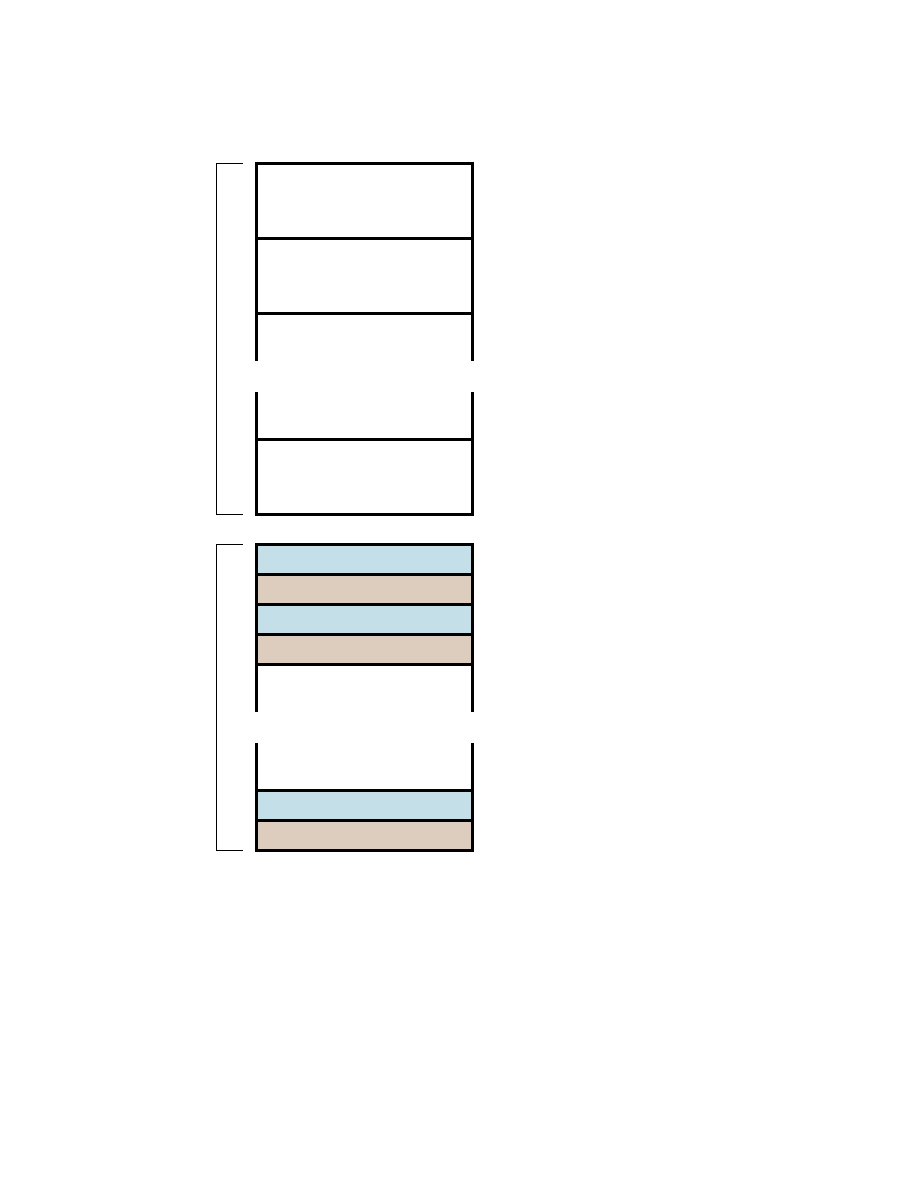
Timings in Function-Only Models
The following table shows the timings used in function-only models of the various types
of Nand Flash.
Model Configuration Strategy
The model uses bits 4:0 of ModelConfig.
Bit 0
●
If bit 0 is set to 1: the default timing values of data transfer from cell to register,
program, and erase are taken as entered from the device datasheet.
●
If bit 0 is set to 0: selected timing parameters are scaled down, and the Power-On
recovery period is bypassed.
For example, if ModelConfig bit 0 is set to 1, then Program Time = 500 us (as specified
in the device datasheet). If bit 0 is set to 0, Program Time = 5 us.
Table 2: Function-Only Timings
Time
Nand Flash Type
Data Transfer from Cell to Register
All
Program
All
Dummy Busy Time for Cache Program
Advanced Nand Flash
Dummy Busy Time for Multiplane Program Multiplane Nand Flash
Block Erase
All
Device Reset (Read)
All
Device Reset (Program)
All
Device Reset (Erase)
All
Device Reset (Erase Suspend)
AMD Nand Flash
Power-On Recovery
All

September 10, 2005
Synopsys, Inc.
9
Nand Flash DesignWare Memory Model Reference
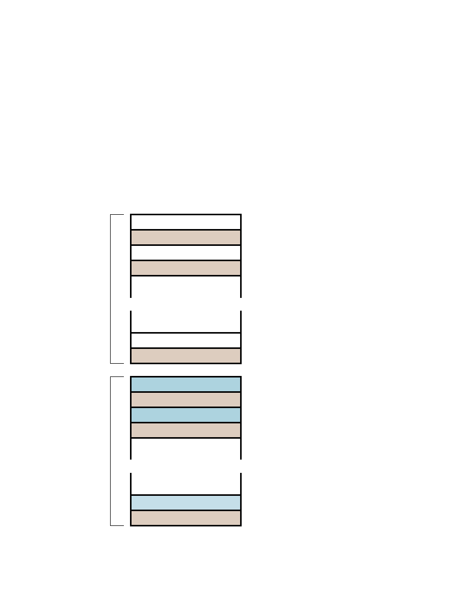
The following parameters are scaled down if ModelConfig bit 0 is set to 0.
Table 3: Basic Nand Flash
Time
Scale Factor
Data transfer from cell to register
1/5
Program
1/100
Block Erase
1/500
Device Reset (Read)
1/2
Device Reset (Program)
1/2
Device Reset (Erase)
1/100
Table 4: AMD Nand Flash
Time
Scale Factor
Data transfer from cell to register
1/10
Program
1/100
Block Erase
1/500
Device Reset (Read)
1/2
Device Reset (Program)
1/2
Device Reset (Erase)
1/100
Device Reset (Erase Suspend)
1/100

10
Synopsys, Inc.
September 10, 2005
Nand Flash DesignWare Memory Model Reference
Bit 1
●
If bit 1 set to 0: This is the Default setting. It will disable tracing (using memcore
commands) of the internal Write operations from the buffer to the memory.
●
If bit 1 set to 1 : It will enable tracing (using memcore commands) of the internal
Write operations from the buffer to the memory.
Bit 2
●
If bit 2 set to 0: This is the Default setting. It will disable tracing (using memcore
commands) of the internal Read operations from the memory to the buffer.
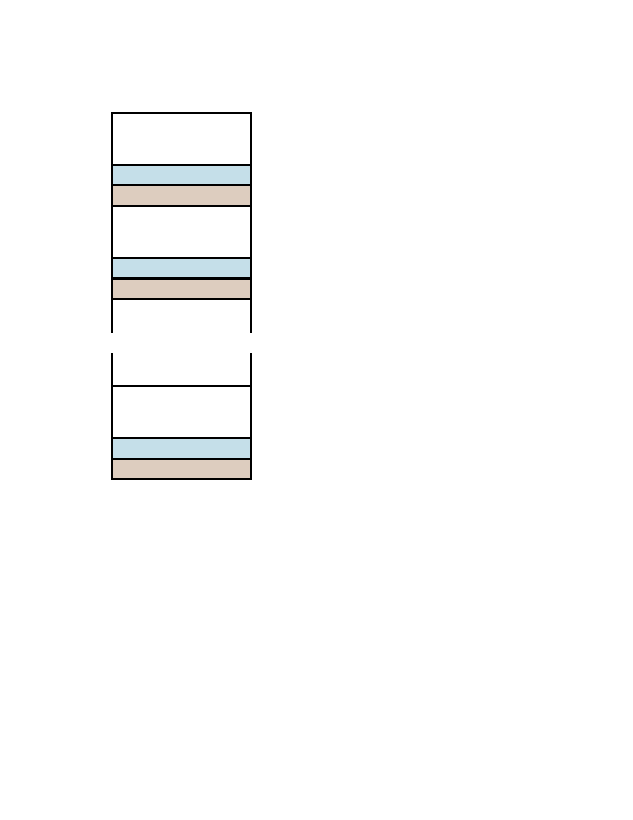
Table 5: Advanced Nand Flash
Time
Scale Factor
Data transfer from cell to register
1/25
Program
1/100
Dummy Busy time for Cache
Program
1/3
Block Erase
1/500
Device Reset (Read)
1/5
Device Reset (Program)
1/2
Device Reset (Erase)
1/100
Table 6: Multiplane Nand Flash
Time
Scale Factor
Data transfer from cell to register
1/10
Program
1/100
Block Erase
1/500
Device Reset (Read)
1/5
Device Reset (Program)
1/2
Device Reset (Erase)
1/100

September 10, 2005
Synopsys, Inc.
11
Nand Flash DesignWare Memory Model Reference
●
If bit 2 set to 1: It will enable tracing (using memcore commands) of the internal
Read operations from the memory to the buffer.
Bit 3
●
If bit 3 set to 0: This is the Default setting.It will disable tracing (using memcore
commands) of the external Write operations to the buffer.
●
If bit 3 set to 1: It will enable tracing (using memcore commands) of the external
Write operations to the buffer.
Bit 4
●
If bit 4 set to 0: This is the Default setting. It will disable tracing (using memcore
commands) of the external Read operations from the buffer.
●
If bit 4 set to 1: It will enable tracing (using memcore commands) of the external
Read operations from the buffer.
Modeling Implementations
Memory Allocation
The memory allocation done in MemCore is illustrated in the following example.
Example: X8 device for Basic Nand Flash, AMD Nand Flash, and
Multiplane Nand Flash
Device Specifications:
❍
Address width: A0–A19
❍
Page size: 512
❍
Spare area: 16
❍
Memcore address width: A0–A19 + one bit Spare_Area_Access: A0–A20
❍
Data width: 8 bit
Since the Spare Area Address bit is not included in the address, an additional bit is
internally appended to the address to access the spare area.
12
Synopsys, Inc.
September 10, 2005
Nand Flash DesignWare Memory Model Reference
The resulting Memcore map is shown below.
Page 0
000000h
to
0001FFh (Main Area — Page 0)
Page 1
000200h
to
0003FFh (Main Area — Page 1)
Main area
.
.
.
.
Page n
0FFE00h
to
0FFFFFh (Main Area — Page n)
100000h to 10000Fh (Spare Area — Page 0)
100010h to 1001FFh (Unused)
100200h to 10020Fh (Spare Area — Page 1)
100210h to 1003FFh (Unused)
Spare area
.
.
.
.
1FFE00h to 1FFE0Fh (Spare Area — Page n)
1FFE10h to 1FFFFFh (Unused)
September 10, 2005
Synopsys, Inc.
13
Nand Flash DesignWare Memory Model Reference
Example: X16 device
Device Specifications:
❍
Address width: A0–A19
❍
Page size: 512
❍
Spare area: 8
❍
Memcore address width: A0–A19 + one bit Spare_Area_Access: A0–A20
❍
Data width: 16 bit
Since the Spare Area Address bit is not included in the address, an additional bit is
internally appended to the address to access the spare area.
The resulting Memcore map is shown below.
For X16 devices, address bit A8 always remains 0.
Page 0
000000h to 0000FFh (Main Area — Page 0)
000100h to 0001FFh (Unused)
Page 1
000200h to 0002FFh (Main Area — Page 1)
000300h to 0003FFh (Unused)
Main area
.
.
.
.
Page n
0FFE00h to 0FFEFFh (Main Area — Page n)
0FFF00h to 0FFFFFh (Unused)
100000h to 100007h (Spare Area — Page 0)
100008h to 1001FFh (Unused)
100200h to 100007h (Spare Area — Page 1)
100208h to 1003FFh (Unused)
Spare area
.
.
.
.
1FFE00h to 1FFE07h (Spare Area — Page n)
1FFE08h to 1FFFFFh (Unused)

14
Synopsys, Inc.
September 10, 2005
Nand Flash DesignWare Memory Model Reference
Example of a Memory Image File
####Main array data
000000/00;
000001/0a;
000002/0b;
000003/0c;
..
..
00ffff/ff;
####Spare array data
100000/89;
100001/64;
100002/51;
100003/21;
Example: X8/X16 device for Advanced Nand Flash
Device Specifications:
❍
Address width: A0–A28
❍
Page size: 2048
❍
Spare area: 16
❍
Memcore address width: A0–A28
❍
Data width: 8 bit
September 10, 2005
Synopsys, Inc.
15
Nand Flash DesignWare Memory Model Reference
The resulting Memcore map is shown below.
Example of a Memory Image File
####Main array data
000000/00;
000001/0a;
000002/0b;
000003/0c;
..
..
00ffff/ff;
####Spare array data
00000800/89;
00000801/64;
00000802/51;
00000803/21;
Page 0
00000000h
to
000007FFh (Main Area — Page 0)
00000800h to 0000080Fh (Spare Area — Page 0)
00000810h to 00000FFFh (Unused)
Page 1
00001000h
to
000017FFh (Main Area — Page 1)
00001800h to 0000180Fh (Spare Area — Page 1)
00001810h to 00001FFFh (Unused)
.
.
.
.
Page n
1FFFF000h
to
1FFFF7FFh (Main Area — Page n)
1FFFF800h to 1FFFF80fh (Spare Area — Page n)
1FFFF810h to 1FFFFFFFh (Unused)

16
Synopsys, Inc.
September 10, 2005
Nand Flash DesignWare Memory Model Reference
The two locations immediately after the end of the spare area of each page are used to
store the partial program count for that page. For example: in the example on
addresses 100010h and 100011h respectively contain the partial program counts for the
Page 0 main array and the spare array.
Initializing a Memory Array and the DefaultData
Attribute
●
The Flash models have the Erase functionality to erase a memory block. To erase
the memory block, the model calls the Custom Model Interface Command
'memcore_unload'.
●
memcore_unload restores the contents of a memory range to the default data value.
●
As per the Flash functionality, when the memory is erased the memory contents are
reset to 1's
●
That is why the default data for the Flash memories needs to be fixed at 1's
●
Therefore, the model does not permit using the DefaultData attribute to initialize a
memory array.
●
The user can, however, initialize large chunks of memory to the desired default data
value through the Memory File MIF as in the following example:
'h000000:'h7fffff/'hE7FF
Document Outline
- Nand Flash Specifications
Wyszukiwarka
Podobne podstrony:
nand flash guide id 313514 Nieznany
nand flash guide
Nand Flash
Wykład VII hazard, realizacja na NAND i NOR
AT89C51 8 bit Microcontroller with 4K Bytes Flash
PIC Programmer All Flash USB Ki Nieznany
Flash i PHP Tworzenie systemu e commerce
Flash on English for Mechanics, Electronics and Technical Assistance
74F10 NAND 3 inp
Flash MX cwiczenia zaawansowane
Pamięci flash
Działanie pamięci flash
jobs flash 3
Flash Lite User Guide Q6J2VKS3J Nieznany
flash BW
flash
więcej podobnych podstron