HEXFET
®
Power MOSFET
PD -91859
Fifth Generation HEXFETs from International Rectifier
utilize advanced processing techniques to achieve
extremely low on-resistance per silicon area. This
benefit, combined with the fast switching speed and
ruggedized device design that HEXFET Power
MOSFETs are well known for, provides the designer
with an extremely efficient and reliable device for use
in a wide variety of applications.
The SO-8 has been modified through a customized
leadframe for enhanced thermal characteristics and
multiple-die capability making it ideal in a variety of
power applications. With these improvements, multiple
devices can be used in an application with dramatically
reduced board space. The package is designed for
vapor phase, infra red, or wave soldering techniques.
Power dissipation of greater than 0.8W is possible in
a typical PCB mount application.
2/24/99
Description
l
Generation V Technology
l
Ultra Low On-Resistance
l
Dual P-Channel Mosfet
l
Surface Mount
l
Available in Tape & Reel
l
Dynamic dv/dt Rating
l
Fast Switching
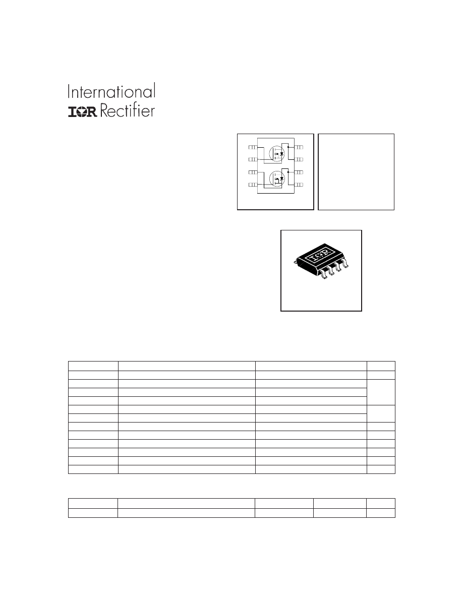
S O -8
V
DSS
= -55V
R
DS(on)
= 0.105
Ω
IRF7342
www.irf.com
1
Parameter
Max.
Units
V
DS
Drain- Source Voltage
-55
V
I
D
@ T
C
= 25°C
Continuous Drain Current, V
GS
@ 10V
-3.4
I
D
@ T
C
= 70°C
Continuous Drain Current, V
GS
@ 10V
-2.7
A
I
DM
Pulsed Drain Current
-27
P
D
@T
C
= 25°C
Power Dissipation
2.0
P
D
@T
C
= 70°C
Power Dissipation
1.3
Linear Derating Factor
0.016
W/°C
V
GS
Gate-to-Source Voltage
± 20
V
V
GSM
Gate-to-Source Voltage Single Pulse tp<10µs
30
V
E
AS
Single Pulse Avalanche Energy
114
dv/dt
Peak Diode Recovery dv/dt
5.0
V/ns
T
J,
T
STG
Junction and Storage Temperature Range
-55 to + 150
°C
Parameter
Typ.
Max.
Units
R
θ
JA
Maximum Junction-to-Ambient
–––
62.5
°C/W
Thermal Resistance
Absolute Maximum Ratings
W
D 1
D 1
D 2
D 2
G 1
S2
G 2
S 1
T op V iew
8
1
2
3
4
5
6
7
IRF7342
2
www.irf.com
Parameter
Min. Typ. Max. Units
Conditions
V
(BR)DSS
Drain-to-Source Breakdown Voltage
-55
–––
–––
V
V
GS
= 0V, I
D
= -250µA
∆
V
(BR)DSS
/
∆
T
J
Breakdown Voltage Temp. Coefficient
––– -0.054 –––
V/°C
Reference to 25°C, I
D
= -1mA
––– 0.095 0.105
V
GS
= -10V, I
D
= -3.4A
––– 0.150 0.170
V
GS
= -4.5V, I
D
= -2.7A
V
GS(th)
Gate Threshold Voltage
-1.0
–––
–––
V
V
DS
= V
GS
, I
D
= -250µA
g
fs
Forward Transconductance
3.3
–––
–––
S
V
DS
= -10V, I
D
= -3.1A
–––
–––
-2.0
V
DS
= -55V, V
GS
= 0V
–––
–––
-25
V
DS
= -55V, V
GS
= 0V, T
J
= 55°C
Gate-to-Source Forward Leakage
–––
–––
-100
V
GS
= -20V
Gate-to-Source Reverse Leakage
–––
–––
100
V
GS
= 20V
Q
g
Total Gate Charge
–––
26
38
I
D
= -3.1A
Q
gs
Gate-to-Source Charge
–––
3.0
4.5
nC
V
DS
= -44V
Q
gd
Gate-to-Drain ("Miller") Charge
–––
8.4
13
V
GS
= -10V, See Fig. 10
t
d(on)
Turn-On Delay Time
–––
14
22
V
DD
= -28V
t
r
Rise Time
–––
10
15
I
D
= -1.0A
t
d(off)
Turn-Off Delay Time
–––
43
64
R
G
= 6.0
Ω
t
f
Fall Time
–––
22
32
R
D
= 16
Ω
,
C
iss
Input Capacitance
–––
690
–––
V
GS
= 0V
C
oss
Output Capacitance
–––
210
–––
pF
V
DS
= -25V
C
rss
Reverse Transfer Capacitance
–––
86
–––
ƒ = 1.0MHz, See Fig. 9
Electrical Characteristics @ T
J
= 25°C (unless otherwise specified)
I
GSS
µA
Ω
R
DS(on)
Static Drain-to-Source On-Resistance
I
DSS
Drain-to-Source Leakage Current
nA
ns
Parameter
Min. Typ. Max. Units
Conditions
I
S
Continuous Source Current
MOSFET symbol
(Body Diode)
showing the
I
SM
Pulsed Source Current
integral reverse
(Body Diode)
p-n junction diode.
V
SD
Diode Forward Voltage
–––
–––
-1.2
V
T
J
= 25°C, I
S
= -2.0A, V
GS
= 0V
t
rr
Reverse Recovery Time
–––
54
80
ns
T
J
= 25°C, I
F
= -2.0A
Q
rr
Reverse RecoveryCharge
–––
85
130
nC
di/dt = -100A/µs
Source-Drain Ratings and Characteristics
–––
–––
–––
–––
-27
-2.0
A
S
D
G
Repetitive rating; pulse width limited by
max. junction temperature. ( See fig. 11 )
I
SD
≤
-3.4A, di/dt
≤
-150A/µs, V
DD
≤
V
(BR)DSS
,
T
J
≤
150°C
Notes:
Starting T
J
= 25°C, L = 20mH
R
G
= 25
Ω
, I
AS
= -3.4A. (See Figure 8)
Pulse width
≤
300µs; duty cycle
≤
2%.
When mounted on 1 inch square copper board, t<10 sec
IRF7342
www.irf.com
3
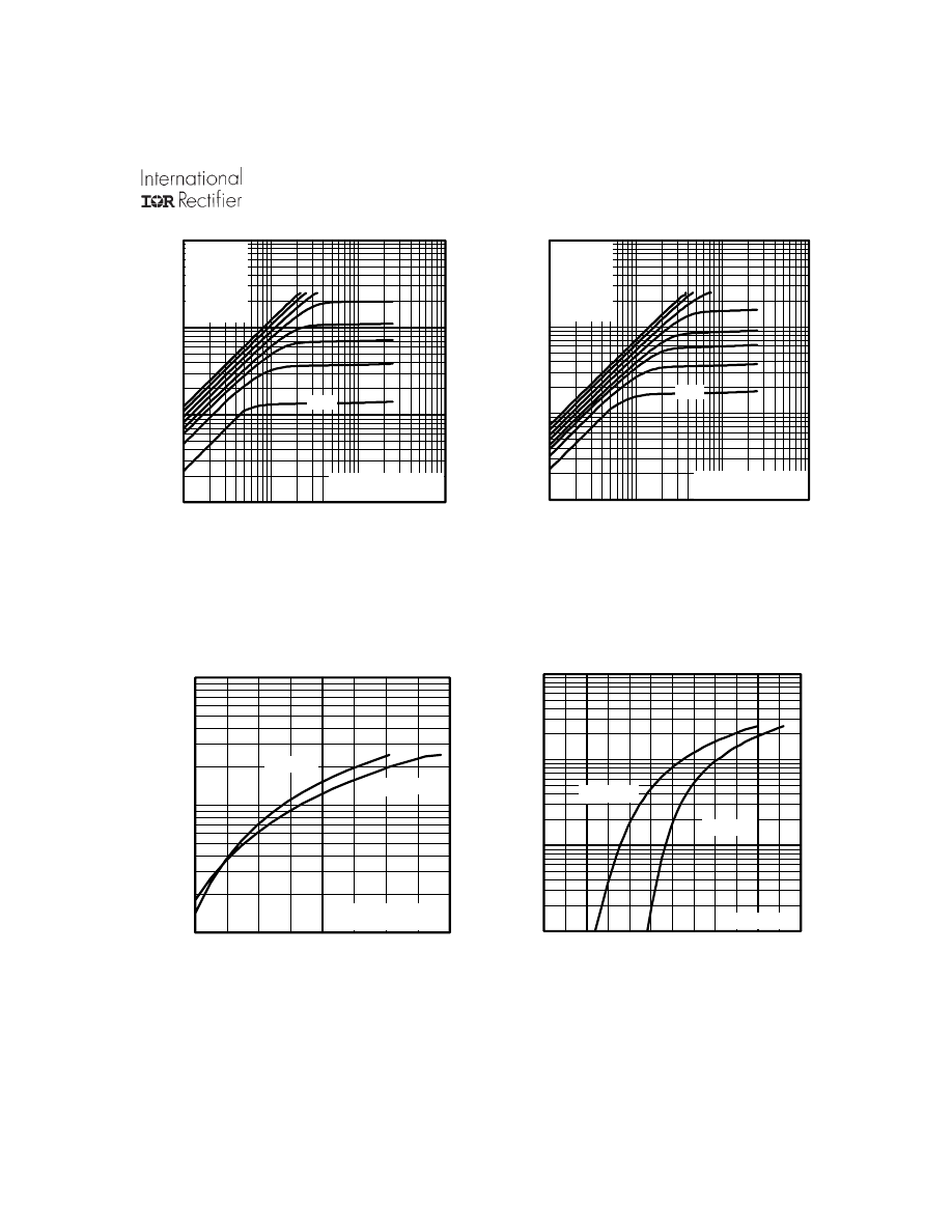
0.1
1
10
100
0.1
1
10
100
20µs PULSE WIDTH
T = 25 C
J
°
TOP
BOTTOM
VGS
-15V
-12V
-10V
-8.0V
-6.0V
-4.0V
-3.5V
-3.0V
-V , Drain-to-Source Voltage (V)
-I , Drain-to-Source Current (A)
DS
D
-3.0V
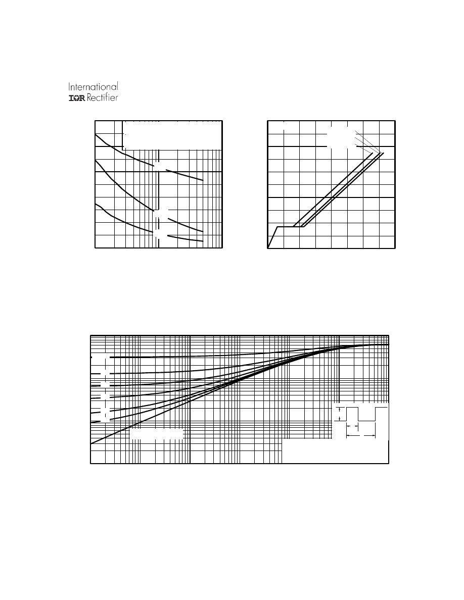
Fig 3. Typical Transfer Characteristics
Fig 2. Typical Output Characteristics
Fig 1. Typical Output Characteristics
Fig 4. Typical Source-Drain Diode
Forward Voltage
0.1
1
10
100
0.1
1
10
100
20µs PULSE WIDTH
T = 150 C
J
°
TOP
BOTTOM
VGS
-15V
-12V
-10V
-8.0V
-6.0V
-4.0V
-3.5V
-3.0V
-V , Drain-to-Source Voltage (V)
-I , Drain-to-Source Current (A)
DS
D
-3.0V
1
10
100
3
4
5
6
7
V = -25V
20µs PULSE WIDTH
DS
-V , Gate-to-Source Voltage (V)
-I , Drain-to-Source Current (A)
GS
D
T = 25 C
J
°
T = 150 C
J
°
0.1
1
10
100
0.2
0.4
0.6
0.8
1.0
1.2
1.4
-V ,Source-to-Drain Voltage (V)
-I , Reverse Drain Current (A)
SD
SD
V = 0 V
GS
T = 25 C
J
°
T = 150 C
J
°
-4.5V
-4.5V
IRF7342
4
www.irf.com
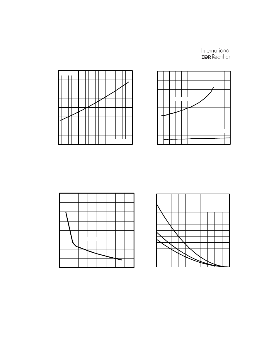
Fig 5. Normalized On-Resistance
Vs. Temperature
Fig 8. Maximum Avalanche Energy
Vs. Drain Current
Fig 6. Typical On-Resistance Vs. Drain
Current
Fig 7. Typical On-Resistance Vs. Gate
Voltage
0
2
4
6
8
10
12
0.080
0.120
0.160
0.200
0.240
R , Drain-to-Source On Resistance
-I , Drain Current (A)
D
DS (on)
VGS = -4.5V
VGS = -10V
(
Ω
)
-60 -40 -20
0
20
40
60
80 100 120 140 160
0.0
0.5
1.0
1.5
2.0
T , Junction Temperature ( C)
R , Drain-to-Source On Resistance
(Normalized)
J
DS(on)
°
V
=
I =
GS
D
-10V
-3.4 A
25
50
75
100
125
150
0
50
100
150
200
250
300
Starting T , Junction Temperature ( C)
E , Single Pulse Avalanche Energy (mJ)
J
AS
°
ID
TOP
BOTTOM
-1.5A
-2.7A
-3.4A
R
DS(on)
, Drain-to-Source On Resistance
( Ω )
0 . 0 5
0 . 1 5
0 . 2 5
0 . 3 5
0 . 4 5
2
5
8
1 1
1 4
A
G S
-V , G ate-to-S ource V oltage (V)
I = -3.4 A
D
IRF7342
www.irf.com
5
0
10
20
30
40
0
4
8
12
16
20
Q , Total Gate Charge (nC)
-V , Gate-to-Source Voltage (V)
G
GS
I =
D
-3.1A
V
= -12V
DS
V
= -30V
DS
V
= -48V
DS
Fig 10. Typical Gate Charge Vs.
Gate-to-Source Voltage
Fig 9. Typical Capacitance Vs.
Drain-to-Source Voltage
Fig 11. Maximum Effective Transient Thermal Impedance, Junction-to-Ambient
-
0.1
1
10
100
0.0001
0.001
0.01
0.1
1
10
100
Notes:
1. Duty factor D =
t / t
2. Peak T = P
x Z
+ T
1
2
J
DM
thJA
A
P
t
t
DM
1
2
t , Rectangular Pulse Duration (sec)
Thermal Response
(Z )
1
thJA
0.01
0.02
0.05
0.10
0.20
D = 0.50
SINGLE PULSE
(THERMAL RESPONSE)
1
10
100
0
240
480
720
960
1200
-V , Drain-to-Source Voltage (V)
C, Capacitance (pF)
DS
V
C
C
C
=
=
=
=
0V,
C
C
C
f = 1MHz
+ C
+ C
C SHORTED
GS
iss
gs
gd ,
ds
rss
gd
oss
ds
gd
C
iss
C
oss
C
rss
IRF7342
6
www.irf.com
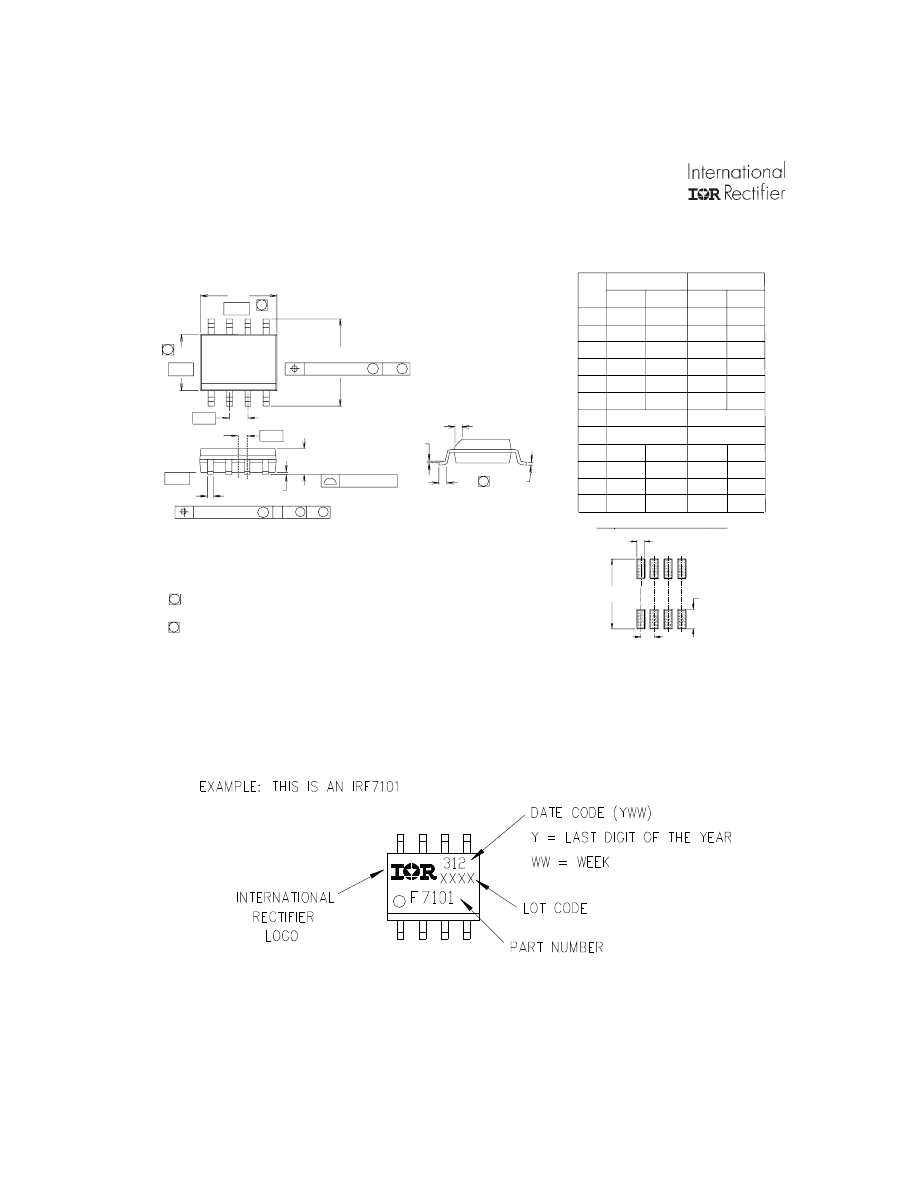
SO-8 Package Details
K x 45 °
C
8X
L
8 X
θ
H
0.2 5 (.0 10 ) M A M
A
0 .10 (.00 4)
B 8X
0 .25 (.01 0) M C A S B S
- C -
6X
e
- B -
D
E
- A -
8 7 6 5
1 2 3 4
5
6
5
R E CO M M E ND E D F O O TP R IN T
0 .72 (.02 8 )
8 X
1 .78 (.07 0)
8X
6 .46 ( .25 5 )
1.27 ( .0 50 )
3X
D IM
IN C H E S M IL LIM E T E R S
M IN M A X M IN M A X
A .0532 .0688 1 .35 1 .75
A 1 .0040 .0098 0 .10 0 .25
B .014 .018 0 .36 0 .46
C .0 075 .0 098 0 .19 0.25
D .1 89 .1 96 4 .80 4.98
E .150 .157 3 .81 3 .99
e .050 B A S IC 1.2 7 B A S IC
e1 .025 B A S IC 0.6 35 B A S IC
H .2 284 .2 440 5 .80 6.20
K .011 .019 0 .28 0 .48
L 0 .16 .050 0 .41 1.27
θ
0° 8° 0 ° 8°
N O TE S :
1 . D IM EN SIO N IN G AN D TO L ER A NC IN G P ER AN S I Y1 4.5 M -198 2.
2 . C O N T RO L LIN G D IM EN SIO N : IN C H .
3 . D IM EN SIO N S A RE SH O W N IN M ILLIM E TE R S (IN C HE S).
4 . O U T LIN E CO N F O RM S T O JED E C O U T LINE M S -0 12 AA .
D IM E NS IO N D O ES N O T IN C LU D E M O LD PR O T R US IO N S
M O LD P R O TR U SIO NS N O T T O EXCE ED 0 .2 5 (.00 6).
D IM E NS IO N S IS T H E LE N G TH O F L EA D F O R SO L DE R IN G TO A SU B ST RA T E..
5
6
A 1
e 1
θ
Part Marking
IRF7342
www.irf.com
7
WORLD HEADQUARTERS: 233 Kansas St., El Segundo, California 90245, Tel: (310) 322 3331
IR GREAT BRITAIN: Hurst Green, Oxted, Surrey RH8 9BB, UK Tel: ++ 44 1883 732020
IR CANADA: 15 Lincoln Court, Brampton, Ontario L6T3Z2, Tel: (905) 453 2200
IR GERMANY: Saalburgstrasse 157, 61350 Bad Homburg Tel: ++ 49 6172 96590
IR ITALY: Via Liguria 49, 10071 Borgaro, Torino Tel: ++ 39 11 451 0111
IR FAR EAST: K&H Bldg., 2F, 30-4 Nishi-Ikebukuro 3-Chome, Toshima-Ku, Tokyo Japan 171 Tel: 81 3 3983 0086
IR SOUTHEAST ASIA: 1 Kim Seng Promenade, Great World City West Tower, 13-11, Singapore 237994 Tel: ++ 65 838 4630
IR TAIWAN:16 Fl. Suite D. 207, Sec. 2, Tun Haw South Road, Taipei, 10673, Taiwan Tel: 886-2-2377-9936
http://www.irf.com/ Data and specifications subject to change without notice. 2/99
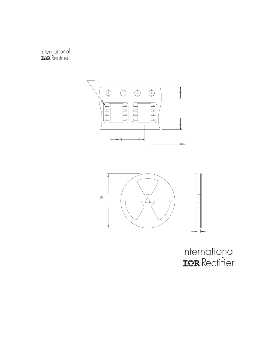
33 0. 0 0
( 1 2 .9 9 2 )
M A X .
1 4 .4 0 ( .5 66 )
1 2 .4 0 ( .4 88 )
N O T E S :
1. C O N T R O L L IN G D IM E N S IO N : M IL L IM E T E R .
2. O U T L IN E C O N F O R M S T O E IA -4 8 1 & E IA - 5 4 1 .
F E E D D IR E C T IO N
T E R M IN A L N U M B E R 1
1 2 .3 ( . 48 4 )
1 1 .7 ( . 46 1 )
8 .1 ( . 31 8 )
7 .9 ( . 31 2 )
N O T E S :
1 . C O N T R O L L IN G D IM E N S IO N : M IL L IM E T E R .
2 . A L L D IM E N S IO N S A R E S H O W N IN M IL L IM E T E R S ( IN C H E S ).
3 . O U T L IN E C O N F O R M S T O E IA -4 8 1 & E IA - 5 4 1 .
Tape and Reel
Wyszukiwarka
Podobne podstrony:
irf7103 HEXFET Power MOSFET id 220258
Ir2111 High Voltage High Speed Power Mosfet And Igbt Driver
POWER MOSFETS
IRF 60W audio Power Amplifier Using Complementary HEXFETs
prezentacja power media
Power D, zebranie zarządu
karty płatnicze (power point)
elastyczność popytu (power point)
kryptologia w bankowości (power point)
europejski system nagród (power point)
TQM zarządzanie jakością (power point)
V80 Power Management 11May04
50w mosfet 540
Popular Mechanics Repairing Power Antennas
więcej podobnych podstron