
DATA SHEET
Preliminary specification
Supersedes data of 2003 Sep 17
2004 Jan 27
INTEGRATED CIRCUITS
TDA1564
High efficiency 2
×
25 W/4
Ω
stereo car radio power amplifier

2004 Jan 27
2
Philips Semiconductors
Preliminary specification
High efficiency 2
×
25 W/4
Ω
stereo car radio power amplifier
TDA1564
FEATURES
•
Low dissipation due to switching from Single-Ended
(SE) to Bridge-Tied Load (BTL) mode
•
Differential inputs with high Common Mode Rejection
Ratio (CMRR)
•
Mute/standby/operating (mode select pin)
•
Load dump protection circuit
•
Short-circuit safe to ground, to supply voltage and
across load
•
Loudspeaker protection circuit
•
Offset detection for each channel
•
Device switches to single-ended operation at excessive
junction temperatures
•
Thermal protection at high junction temperature (170
°
C)
•
Clip detection at THD = 2.5 %
•
Diagnostic information
(clip/protection/prewarning/offset).
GENERAL DESCRIPTION
The TDA1564 is a monolithic power amplifier in a 17-lead
single-in-line (SIL) plastic power package. It contains two
identical 25 W amplifiers. The dissipation is minimized by
switching from SE to BTL mode, only when a higher output
voltage swing is needed. The device is primarily
developed for car radio applications.
QUICK REFERENCE DATA
ORDERING INFORMATION
SYMBOL
PARAMETER
CONDITIONS
MIN.
TYP.
MAX.
UNIT
V
P
supply voltage
DC biased
6.0
14.4
18
V
non-operating
−
−
30
V
load dump
−
−
45
V
I
ORM
repetitive peak output current
−
−
4
A
I
q(tot)
total quiescent current
R
L
=
∞
−
95
150
mA
I
stb
standby current
−
1
50
µ
A
Z
i
input impedance
90
120
150
k
Ω
P
o
output power
R
L
= 4
Ω
; EIAJ
−
38
−
W
R
L
= 4
Ω
; THD = 10 %
23
25
−
W
R
L
= 4
Ω
; THD = 2.5 %
18
20
−
W
G
v
voltage gain
P
o
= 1 W
25
26
27
dB
CMRR
common mode rejection ratio
f = 1 kHz; R
s
= 0
Ω
−
80
−
dB
SVRR
supply voltage ripple rejection
f = 1 kHz; R
s
= 0
Ω
45
65
−
dB
∆
V
O
DC output offset voltage
−
−
100
mV
α
cs
channel separation
R
s
= 0
Ω
; P
o
= 15 W
40
70
−
dB
∆
G
v
channel unbalance
−
−
1
dB
TYPE
NUMBER
PACKAGE
NAME
DESCRIPTION
VERSION
TDA1564TH
HSOP20
plastic, heatsink small outline package; 20 leads; low stand-off height
SOT418-3
TDA1564J
DBS17P
plastic DIL-bent-SIL power package; 17 leads (lead length 12 mm)
SOT243-1
2004 Jan 27
3
Philips Semiconductors
Preliminary specification
High efficiency 2
×
25 W/4
Ω
stereo car radio power amplifier
TDA1564
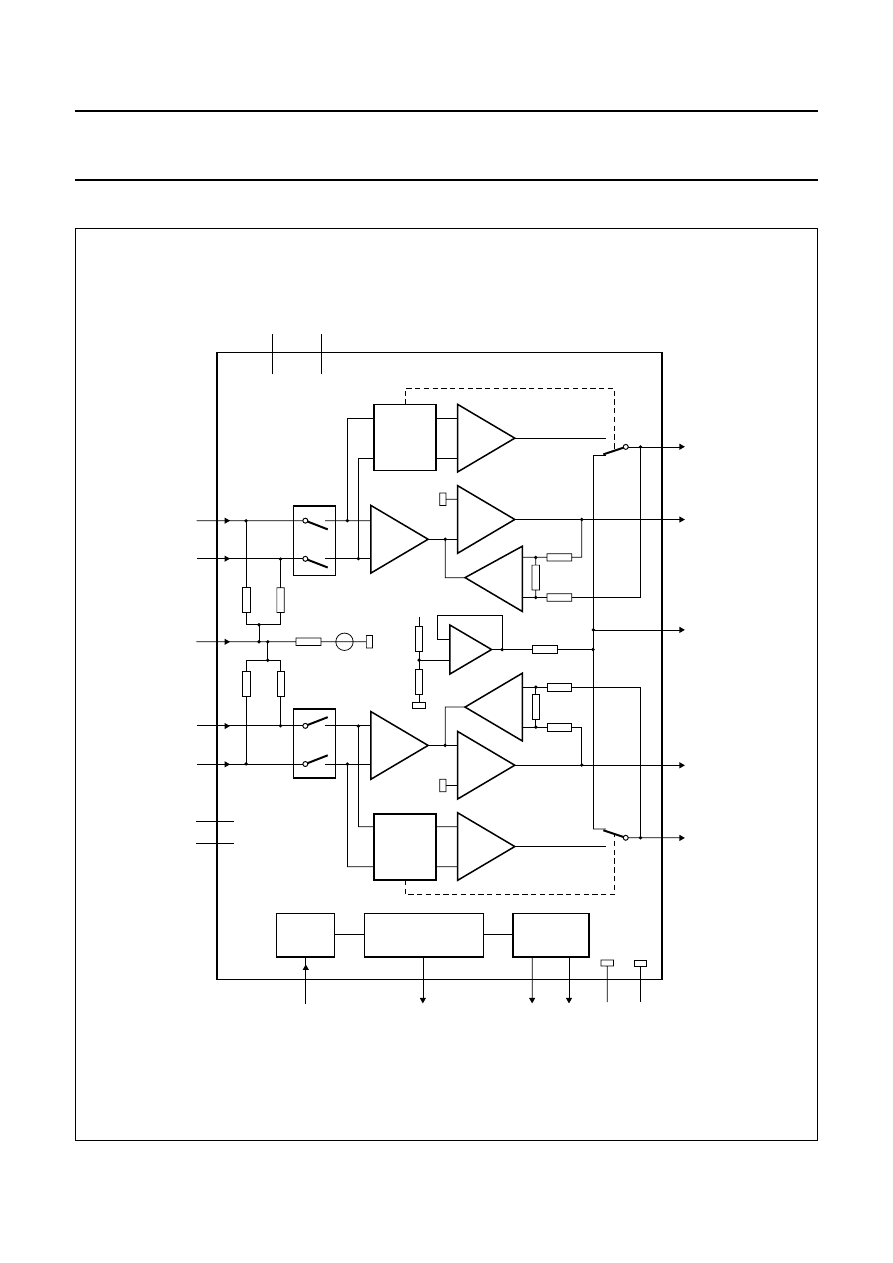
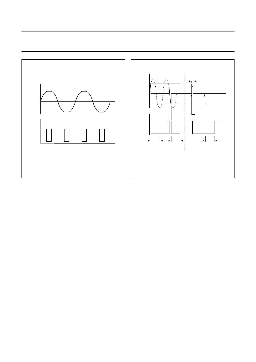
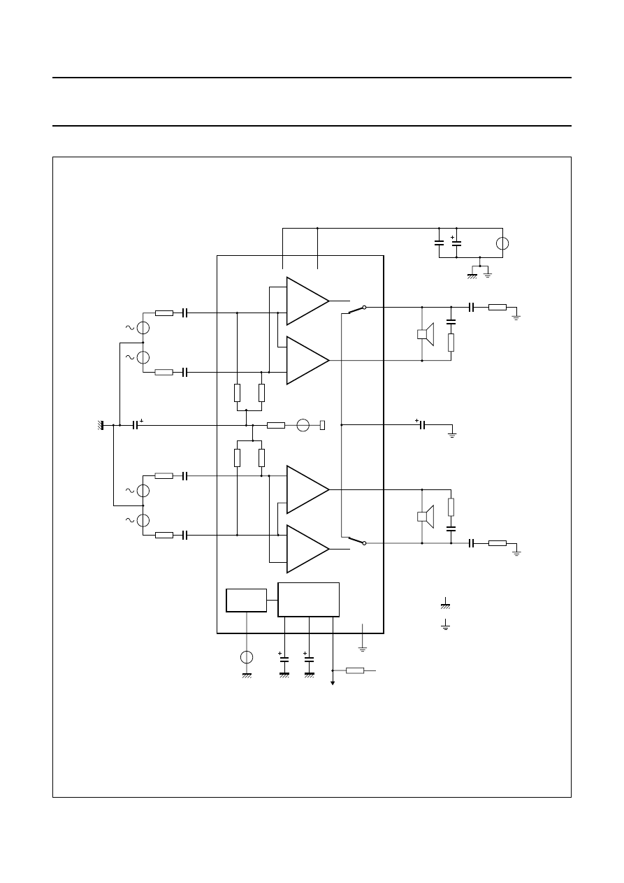
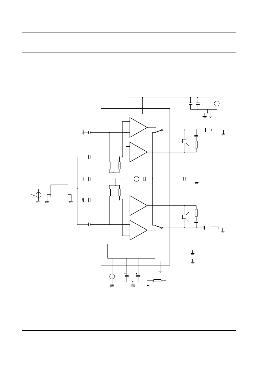
BLOCK DIAGRAM
mdb811
+
−
+
−
+
−
+
−
MUTE
VI
VI
VI
IV
IV
VI
SLAVE
CONTROL
14
13
IN2
+
19
CIN
1
n.c.
10
n.c.
IN2
−
60
k
Ω
60
k
Ω
60
k
Ω
60
k
Ω
25 k
Ω
V
ref
OUT2
−
OUT2
+
7
8
CSE
16
+
−
+
−
+
−
+
−
MUTE
SLAVE
CONTROL
17
18
IN1
+
IN1
−
OUT1
+
OUT1
−
4
3
+
−
V
P
STANDBY
LOGIC
CLIP/PROTECTION
TEMP PREWARNING
2
15
12
MODE
OFFSET
DETECTION
DIAG
OC1
9
OC2
GND1
5
GND2
6
V
P2
11
V
P1
20
TDA1564TH
Fig.1 Block diagram (TDA1564TH).
2004 Jan 27
4
Philips Semiconductors
Preliminary specification
High efficiency 2
×
25 W/4
Ω
stereo car radio power amplifier
TDA1564
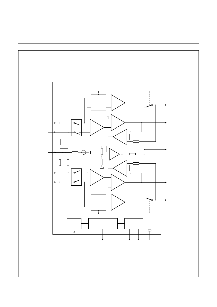
mgw244
+
−
+
−
+
−
+
−
MUTE
VI
VI
VI
IV
IV
VI
SLAVE
CONTROL
17
16
IN2
+
3
CIN
IN2
−
60
k
Ω
60
k
Ω
60
k
Ω
60
k
Ω
25 k
Ω
V
ref
OUT2
−
OUT2
+
10
11
CSE
4
+
−
+
−
+
−
+
−
MUTE
SLAVE
CONTROL
1
2
IN1
+
IN1
−
OUT1
+
OUT1
−
8
7
+
−
V
P
STANDBY
LOGIC
CLIP/PROTECTION
TEMP PREWARNING
6
15
14
MODE
OFFSET
DETECTION
DIAG
OC1
12
OC2
GND
9
V
P2
13
V
P1
5
TDA1564J
Fig.2 Block diagram (TDA1564J).

2004 Jan 27
5
Philips Semiconductors
Preliminary specification
High efficiency 2
×
25 W/4
Ω
stereo car radio power amplifier
TDA1564
PINNING
SYMBOL
PIN
DESCRIPTION
TDA1564TH
TDA1564J
n.c.
1
−
not connected
MODE
2
6
mute/standby/operating
OUT1
−
3
7
inverting output 1
OUT1+
4
8
non-inverting output 1
GND1
5
−
ground 1
GND
−
9
ground
GND2
6
−
ground 2
OUT2
−
7
10
inverting output 2
OUT2+
8
11
non-inverting output 2
OC2
9
12
offset capacitor 2
n.c.
10
−
not connected
V
P2
11
13
supply voltage 2
OC1
12
14
offset capacitor 1
IN2
−
13
16
inverting input 2
IN2+
14
17
non-inverting input 2
DIAG
15
15
diagnostic
CSE
16
4
electrolytic capacitor for single-ended (SE) mode
IN1+
17
1
non-inverting input 1
IN1
−
18
2
inverting input 1
CIN
19
3
common input
V
P1
20
5
supply voltage 1
2004 Jan 27
6
Philips Semiconductors
Preliminary specification
High efficiency 2
×
25 W/4
Ω
stereo car radio power amplifier
TDA1564
TDA1564TH
V
P1
n.c.
CIN
MODE
IN1
−
OUT1
−
IN1
+
OUT1
+
CSE
GND1
DIAG
GND2
IN2
+
OUT2
−
IN2
−
OUT2
+
OC1
OC2
V
P2
n.c.
001aaa307
20
19
18
17
16
15
14
13
12
11
9
10
7
8
5
6
3
4
1
2
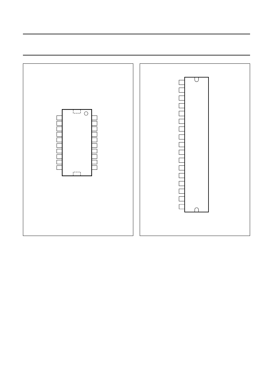
Fig.3 Pin configuration (TDA1564TH).
handbook, halfpage
TDA1564J
MGW245
IN1
+
IN1
−
CIN
CSE
VP1
MODE
OUT1
−
OUT1
+
GND
OUT2
−
OUT2
+
OC2
VP2
OC1
DIAG
IN2
−
IN2
+
1
2
3
4
5
6
7
8
9
10
11
12
13
14
15
16
17
Fig.4 Pin configuration (TDA1564J).
FUNCTIONAL DESCRIPTION
The TDA1564 contains two identical amplifiers with
differential inputs. At low output power [up to output
amplitudes of 3 V (RMS) at V
P
= 14.4 V], the device
operates as a normal SE amplifier. When a larger output
voltage swing is needed, the circuit switches internally to
BTL operation.
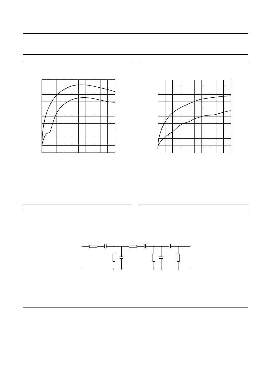
With a sine wave input signal, the dissipation of a
conventional BTL amplifier (up to 2 W output power) is
more than twice the dissipation of the TDA1564 (see
Fig.12).
In normal use, when the amplifier is driven with music-like
signals, the high (BTL) output power is only needed for a
small percentage of time. Assuming that a music signal
has a normal (Gaussian) amplitude distribution, the
dissipation of a conventional BTL amplifier with the same
output power is approximately 70 % higher (see Figs 13
and 14.
The heatsink has to be designed for use with music
signals. With such a heatsink, the thermal protection will
disable the BTL mode when the junction temperature
exceeds 150
°
C. In this case, the output power is limited to
5 W per amplifier.
The gain of each amplifier is internally fixed at 26 dB. The
device can be switched to the following modes via the
MODE pin:
•
Standby with low standby current (< 50
µ
A)
•
Mute condition, DC adjusted
•
On, operation.
The device is fully protected against a short-circuit of the
output pins to ground and to the supply voltage. It is also
protected against a short-circuit of the loudspeaker and
against high junction temperatures. In the event of a
permanent short-circuit condition to ground or the supply
voltage, the output stage will be switched off, causing low
dissipation. With a permanent short-circuit of the

2004 Jan 27
7
Philips Semiconductors
Preliminary specification
High efficiency 2
×
25 W/4
Ω
stereo car radio power amplifier
TDA1564
loudspeaker, the output stage will be repeatedly switched
on and off. The duty cycle in the ‘on’ condition is low
enough to prevent excessive dissipation.
The device also has two independent DC offset detection
circuits that can detect DC output voltages across the
speakers. With a DC offset greater than 2 V, a warning is
given on the diagnostic pin. There will be no internal
shutdown with DC offsets.
When the supply voltage drops below 6 V (e.g. engine
start), the circuit mutes immediately, avoiding clicks from
the electronic circuit preceding the power amplifier.
The voltage of the SE electrolytic capacitor (pin 4) is kept
at 0.5V
P
by means of a voltage buffer (see Fig.2). The
value of this capacitor has an important influence on the
output power in SE mode, especially at low signal
frequencies. A high value is recommended to minimize
dissipation at low frequencies.
The diagnostic output is an open-collector output and
requires a pull-up resistor. It gives the following outputs:
•
Clip detection at THD = 2.5 %
•
Short-circuit protection:
– When a short-circuit occurs (for at least 10 ms) at the
outputs to ground or the supply voltage, the output
stages are switched off to prevent excessive
dissipation; the outputs are switched on again
approximately 500 ms after the short-circuit is
removed, during this short-circuit condition the
protection pin is LOW
– When a short-circuit occurs across the load (for at
least 10 ms), the output stages are switched off for
approximately 500 ms; after this time, a check is
made to see whether the short-circuit is still present
– The power dissipation in any short-circuit condition is
very low.
•
During start-up/shutdown, when the product is internally
muted
•
Temperature prewarning:
– A prewarning (junction temperature > 145
°
C)
indicates that the temperature protection will become
active. The prewarning can be used to reduce the
input signal and thus reduce the power dissipation.
•
Offset detection:
– One of the channels has a DC output voltage greater
than 2 V.
LIMITING VALUES
In accordance with the Absolute Maximum Rating System (IEC 60134).
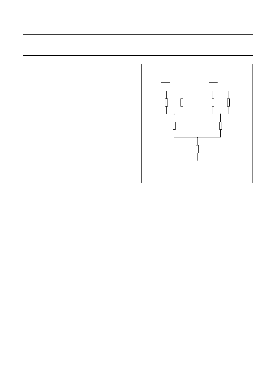
THERMAL CHARACTERISTICS
Note
1. The value of R
th(c-h)
depends on the application (see Fig.5).
SYMBOL
PARAMETER
CONDITIONS
MIN.
MAX.
UNIT
V
P
supply voltage
operating
−
18
V
non-operating
−
30
V
load dump; t
r
>
2.5 ms
−
45
V
V
P(sc)
short-circuit safe voltage
−
18
V
V
rp
reverse polarity voltage
−
6
V
I
ORM
repetitive peak output current
−
4
A
P
tot
total power dissipation
−
60
W
T
stg
storage temperature
−
55
+150
°
C
T
vj
virtual junction temperature
−
150
°
C
T
amb
ambient temperature
−
40
+85
°
C
SYMBOL
PARAMETER
CONDITIONS
VALUE
UNIT
R
th(j-c)
thermal resistance from junction to case
note 1
1.3
K/W
R
th(j-a)
thermal resistance from junction to ambient
in free air
40
K/W
2004 Jan 27
8
Philips Semiconductors
Preliminary specification
High efficiency 2
×
25 W/4
Ω
stereo car radio power amplifier
TDA1564
Heatsink design
There are two parameters that determine the size of the
heatsink. The first is the rating for the virtual junction
temperature and the second is the ambient temperature at
which the amplifier must still deliver its full power in the
BTL mode.
With a conventional BTL amplifier, the maximum power
dissipation with a music-like signal (at each amplifier) will
be approximately two times 6.5 W. At a virtual junction
temperature of 150
°
C and a maximum ambient
temperature of 65
°
C, R
th(vj-c)
= 1.3 K/W and
R
th(c-h)
= 0.2 K/W, the thermal resistance of the heatsink
should be:
Compared to a conventional BTL amplifier, the TDA1564
has a higher efficiency. The thermal resistance of the
heatsink should be:
150
65
–
2
6.5
×
----------------------
1.3
–
0.2
–
5 K/W
=
1.7
145
65
–
2
6.5
×
----------------------
1.3
–
0.2
–
9 K/W
=
Fig.5 Thermal equivalent resistance network.
handbook, halfpage
3.6 K/W
0.6 K/W
3.6 K/W
virtual junction
OUT 1
OUT 1
case
3.6 K/W
0.6 K/W
3.6 K/W
OUT 2
OUT 2
MGC424
0.1 K/W

2004 Jan 27
9
Philips Semiconductors
Preliminary specification
High efficiency 2
×
25 W/4
Ω
stereo car radio power amplifier
TDA1564
DC CHARACTERISTICS
V
P
= 14.4 V; T
amb
= 25
°
C; measured in Fig.9; unless otherwise specified.
Notes
1. The circuit is DC biased at V
P
= 6 to 18 V and AC operating at V
P
= 8 to 18 V.
2. If the junction temperature exceeds 150
°
C, the output power is limited to 5 W per channel.
SYMBOL
PARAMETER
CONDITIONS
MIN.
TYP.
MAX.
UNIT
Supplies
V
P
supply voltage
note 1; Fig.17
6.0
14.4
18.0
V
I
q(tot)
total quiescent current
R
L
=
∞
−
95
150
mA
I
stb
standby current
−
1
50
µ
A
V
CSE
average electrolytic capacitor
voltage at pin 4
−
7.1
−
V
∆
V
O
DC output offset voltage
on state
−
−
100
mV
mute state
−
−
100
mV
Mode select switch; see Fig.6
V
MODE
voltage at mode select pin
standby condition
0
−
1
V
mute condition
2
−
3
V
on condition
4
5
V
P
V
I
MODE(sw)
switch current through pin 6
V
MODE
= 5 V
−
25
40
µ
A
Diagnostic
V
DIAG
output voltage at the
diagnostic output pin
I
DIAG
= 2 mA; during any fault
condition or clip detect
−
−
0.5
V
I
DIAG
current through the diagnostic
pin
during any fault condition or
clip detect
2
−
−
mA
V
O(DC)
DC output voltage detection
levels
1.4
2
2.5
V
Protection
T
pre
prewarning temperature
−
145
−
°
C
T
dis(BTL)
BTL disable temperature
note 2
−
150
−
°
C
2004 Jan 27
10
Philips Semiconductors
Preliminary specification
High efficiency 2
×
25 W/4
Ω
stereo car radio power amplifier
TDA1564
handbook, halfpage
MGR176
18
VMODE
(V)
4
3
2
1
0
Mute
Operating
Standby
Fig.6 Switching levels of the mode select pin.

2004 Jan 27
11
Philips Semiconductors
Preliminary specification
High efficiency 2
×
25 W/4
Ω
stereo car radio power amplifier
TDA1564
AC CHARACTERISTICS
V
P
= 14.4 V; R
L
= 4
Ω
; C
CSE
= 1000
µ
F; f = 1 kHz; T
amb
= 25
°
C; measured in Fig.9; unless otherwise specified.
Notes
1. The distortion is measured with a bandwidth of 10 Hz to 30 kHz.
2. Frequency response externally fixed (input capacitors determine the low frequency roll-off).
3. The SE to BTL switch voltage level depends on the value of V
P
.
4. Noise output voltage measured with a bandwidth of 20 Hz to 20 kHz.
5. Noise output voltage is independent of R
s
.
SYMBOL
PARAMETER
CONDITIONS
MIN.
TYP.
MAX.
UNIT
P
o
output power
THD = 0.5 %; Fig.18
15
19
−
W
THD = 10 %; Fig.18
23
25
−
W
EIAJ
−
38
−
W
V
P
= 13.2 V; THD = 0.5 %
−
16
−
W
V
P
= 13.2 V; THD = 10 %
−
20
−
W
THD
total harmonic distortion
P
o
= 1 W; note 1; Fig.19
−
0.1
−
%
P
power dissipation
see Figs 12 and 13
W
B
p
power bandwidth
THD = 1 %; P
o
=
−
1 dB with
respect to 15 W
−
20 to
15000
−
Hz
f
ro(l)
low frequency roll-off
−
1 dB; note 2
−
25
−
Hz
f
ro(h)
high frequency roll-off
−
1 dB
130
−
−
kHz
G
v
closed-loop voltage gain
P
o
= 1 W; Fig.21
25
26
27
dB
SVRR
supply voltage ripple rejection
R
s
= 0
Ω
; V
ripple
= 2 V (p-p); Fig.22
on/mute
45
65
−
dB
standby; f = 100 Hz to 10 kHz
45
−
−
dB
CMRR
common mode rejection ratio
R
s
= 0
Ω
70
90
−
dB
Z
i
input impedance
90
120
150
k
Ω
∆
Z
i
mismatch in input impedance
−
1
−
%
V
SE-BTL
SE to BTL switch voltage level
note 3
−
3
−
V
V
out
output voltage mute (RMS value)
V
i
= 1 V (RMS)
−
100
150
µ
V
V
n(o)
noise output voltage
on; R
s
= 0
Ω
; note 4
−
100
150
µ
V
on; R
s
= 10 k
Ω
; note 4
−
105
−
µ
V
mute; note 5
−
100
150
µ
V
α
cs
channel separation
R
s
= 0
Ω
; P
o
= 15 W; Fig.23
40
70
−
dB
∆
G
v
channel unbalance
−
−
1
dB
2004 Jan 27
12
Philips Semiconductors
Preliminary specification
High efficiency 2
×
25 W/4
Ω
stereo car radio power amplifier
TDA1564
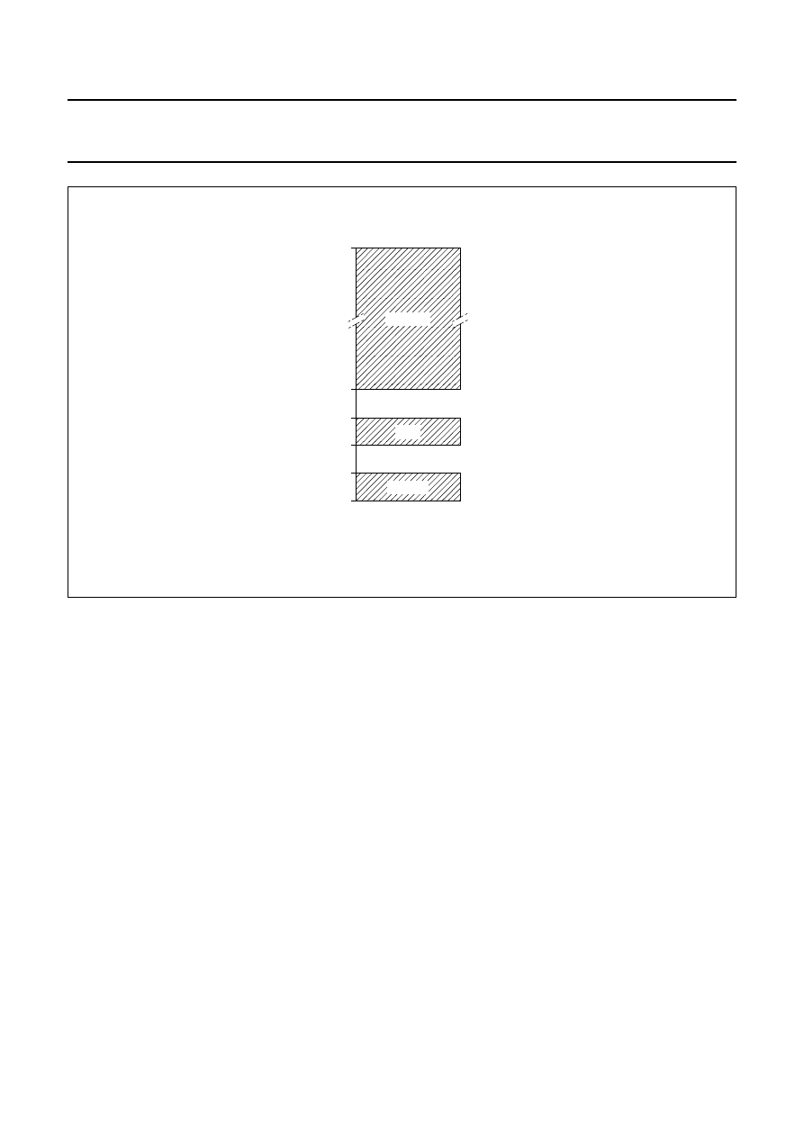
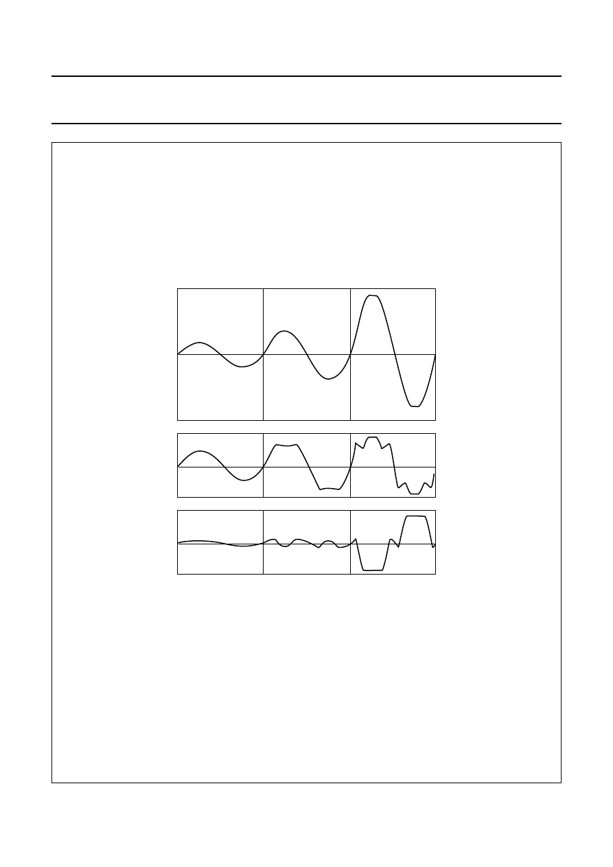
handbook, halfpage
MGR177
Vo
CLIP
0
0
t
Fig.7 Clip detection waveforms.
handbook, halfpage
MGW246
maximum current
short-circuit to supply pins
short-circuit
to ground
short-circuit
removed
500
ms
500
ms
500
ms
10
µ
s
Io
DIAG
0
max
max
t
t
Fig.8 Protection waveforms.
(1)
2004 Jan 27
13
Philips Semiconductors
Preliminary specification
High efficiency 2
×
25 W/4
Ω
stereo car radio power amplifier
TDA1564
TEST AND APPLICATION INFORMATION
handbook, full pagewidth
MGW247
3
CIN
25 k
Ω
60
k
Ω
60
k
Ω
60
k
Ω
60
k
Ω
Vref
OUT2
−
OUT2
+
10
11
CSE
4
2
IN1
−
1
IN1
+
OUT1
+
OUT1
−
8
7
STANDBY
LOGIC
CLIP AND
DIAGNOSTIC
6
12
14
15
MODE
OC2
OC1
DIAG
9
GND
VP2
13
VP1
5
TDA1564J
10
µ
F
1000
µ
F
220 nF
0.5Rs
220 nF
0.5Rs
+
−
+
−
Vms
VP
Vlogic
Rpu
16
IN2
−
17
IN2
+
220 nF
0.5Rs
100 nF
100 nF
3.9
Ω
4
Ω
3.9
Ω
100 nF
100 nF
3.9
Ω
4
Ω
3.9
Ω
220 nF
0.5Rs
+
−
+
−
220 nF
2200
µ
F
signal ground
power ground
22
µ
F
22
µ
F
Fig.9 Application diagram (TDA1564J).
Connect Boucherot filter to pin 8 or pin 10 with the shortest possible connection.
2004 Jan 27
14
Philips Semiconductors
Preliminary specification
High efficiency 2
×
25 W/4
Ω
stereo car radio power amplifier
TDA1564
handbook, full pagewidth
MGW248
sgnd
sgnd
diag
RL
2000
On
Mute
TDA1564J
TDA1565J
Off
In2
In1
GND
VP
Out1
Out2
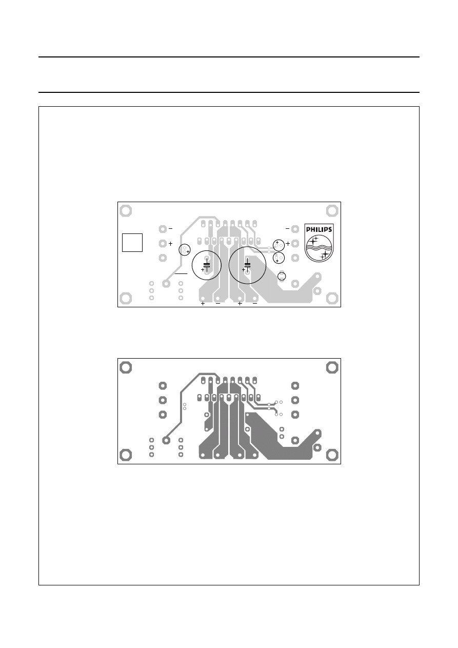
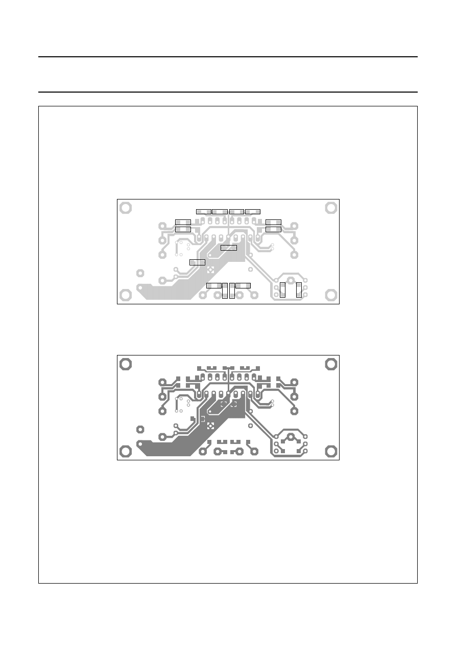
Fig.10 PCB layout (component side) for the application of Fig.9.
Dimensions in mm.
2004 Jan 27
15
Philips Semiconductors
Preliminary specification
High efficiency 2
×
25 W/4
Ω
stereo car radio power amplifier
TDA1564
handbook, full pagewidth
MGW249
In2
GND
High efficiency
Cool
Power
Continuous offset detection
In1
1
17
Out1
Out2
VP
220 nF
220 nF
220 nF
100 nF
100 nF
100 nF
100 nF
4.7 k
Ω
2.7 k
Ω
24 k
Ω
3.9
Ω
3.9
Ω
3.9
Ω
Fig.11 PCB layout (soldering side) for the application of Fig.9.
Dimensions in mm.
2004 Jan 27
16
Philips Semiconductors
Preliminary specification
High efficiency 2
×
25 W/4
Ω
stereo car radio power amplifier
TDA1564
handbook, halfpage
0
20
25
0
5
MGW250
10
15
20
4
8
(1)
(2)
12
16
Po (W)
P
(W)
Fig.12 Power dissipation as a function of output
power; sine wave driven.
Input signal 1 kHz, sinusoidal; V
P
= 14.4 V.
(1) For a conventional BTL amplifier.
(2) For TDA1564.
handbook, halfpage
0
10
25
0
5
MGW251
10
15
20
2
4
(1)
(2)
6
8
Po (W)
P
(W)
Fig.13 Power dissipation as a function of output
power; pink noise through IEC-60268 filter.
(1) For a conventional BTL amplifier.
(2) For TDA1564.
430
Ω
input
output
330
Ω
3.3
k
Ω
3.3
k
Ω
10
k
Ω
91
nF
68
nF
470 nF
2.2
µ
F
2.2
µ
F
MGC428
Fig.14 IEC-60268 filter.
2004 Jan 27
17
Philips Semiconductors
Preliminary specification
High efficiency 2
×
25 W/4
Ω
stereo car radio power amplifier
TDA1564
handbook, full pagewidth
MGW252
3
CIN
25 k
Ω
60
k
Ω
60
k
Ω
60
k
Ω
60
k
Ω
Vref
OUT2
−
OUT2
+
10
11
CSE
4
2
IN1
−
1
IN1
+
OUT1
+
OUT1
−
8
7
VP2
13
VP1
5
TDA1564J
10
µ
F
1000
µ
F
220 nF
220 nF
IEC-60268
FILTER
pink
noise
+
−
+
−
VP
16
IN2
−
17
IN2
+
220 nF
100 nF
100 nF
3.9
Ω
4
Ω
3.9
Ω
100 nF
100 nF
3.9
Ω
4
Ω
3.9
Ω
220 nF
+
−
+
−
220 nF
2200
µ
F
signal ground
power ground
INTERFACE
6
12
14
15
MODE
OC2
OC1
DIAG
DIAG
OFFSET
MS
9
GND
Vms
Vlogic
Rpu
22
µ
F
22
µ
F
Fig.15 Test and application diagram for dissipation measurements with a music-like signal (pink noise).
2004 Jan 27
18
Philips Semiconductors
Preliminary specification
High efficiency 2
×
25 W/4
Ω
stereo car radio power amplifier
TDA1564
Fig.16 Quiescent current as a function of supply
voltage.
V
MODE
= 5 V; R
I
=
∞
.
handbook, halfpage
0
5
10
20
15
25
150
50
0
100
MGW253
VP (V)
IP
(mA)
handbook, halfpage
0
200
100
150
50
0
1
1
5
MGW254
2
2
3
3
4
VMODE (V)
IP
(mA)
Fig.17 Supply current as a function of V
MODE
.
V
P
= 14.4 V
(1) Standby.
(2) Mute.
(3) Operating.
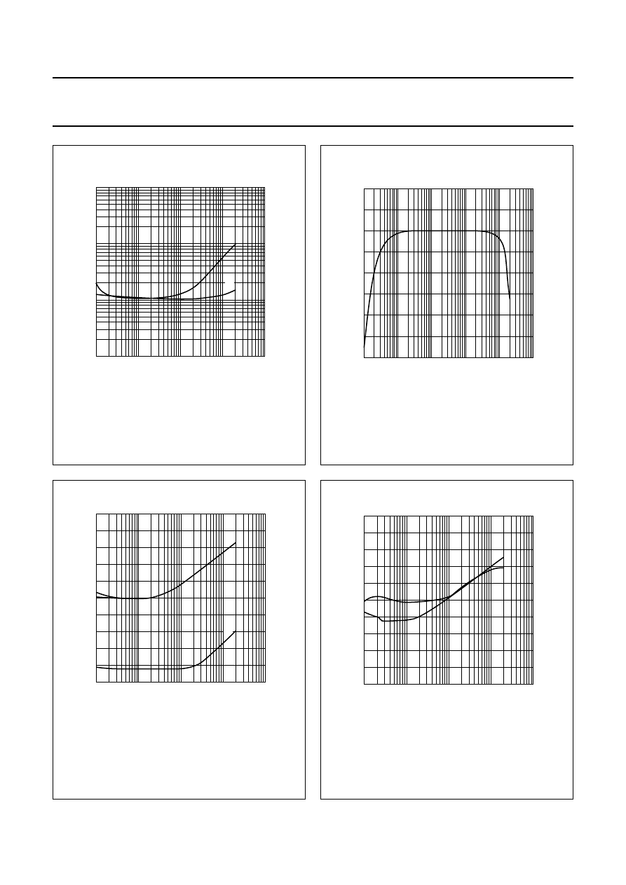
handbook, halfpage
8
40
20
30
10
0
10
18
MGW255
12
14
16
VP (V)
(1)
(2)
(3)
Po
(W)
Fig.18 Output power as a function of supply
voltage.
(1) TDH + N = 10 %.
(2) TDH + N = 2.5 %.
(3) TDH + N = 0.5 %.
handbook, halfpage
MGW256
10
−
1
1
Po (W)
THD
+
N
(%)
10
10
2
10
−
2
10
−
2
10
−
1
1
10
10
2
(2)
(3)
(1)
Fig.19 THD + noise as a function of output power.
(1) f = 10 kHz.
(2) f = 1 kHz.
(3) f = 100 kHz.
2004 Jan 27
19
Philips Semiconductors
Preliminary specification
High efficiency 2
×
25 W/4
Ω
stereo car radio power amplifier
TDA1564
handbook, halfpage
MGW257
THD
+
N
(%)
10
−
2
10
−
1
1
10
10
10
2
10
3
10
4
10
5
f (Hz)
(1)
(2)
Fig.20 THD + noise as a function of frequency.
(1) P
o
= 10 W.
(2) P
o
= 1 W.
handbook, halfpage
20
24
28
26
22
MGW258
10
Gv
(dB)
10
2
10
3
10
4
10
5
f (Hz)
10
6
Fig.21 Voltage gain as a function of frequency.
handbook, halfpage
−
120
−
20
−
100
−
80
−
60
−
40
MGW259
10
10
2
10
3
10
4
10
5
f (Hz)
SVRR
(dB)
(1)
(2)
Fig.22 SVRR as a function of frequency.
(1) On/Mute.
(2) Standby.
handbook, halfpage
−
120
−
20
−
100
−
80
−
60
−
40
MGW260
10
10
2
10
3
10
4
10
5
f (Hz)
α
cs
(dB)
(1)
(2)
Fig.23 Channel separation as a function of
frequency.
(1) P
o2
= 10 W.
(2) P
o2
= 1 W.
2004 Jan 27
20
Philips Semiconductors
Preliminary specification
High efficiency 2
×
25 W/4
Ω
stereo car radio power amplifier
TDA1564
handbook, full pagewidth
MBH691
0
1
2
t (ms)
3
1/2 VP
1/2 VP
0
−
VP
VP
VP
0
VP
Vload
Vmaster
Vslave
0
Fig.24 Output waveforms.
V
load
= V
7
−
V
8
or V
11
−
V
10
.
V
master
= V
7
or V
11
.
V
slave
= V
8
or V
10
.
2004 Jan 27
21
Philips Semiconductors
Preliminary specification
High efficiency 2
×
25 W/4
Ω
stereo car radio power amplifier
TDA1564
APPLICATION NOTES
Advantages of high efficiency
1. Power conversion improvement (power supply):
Usually, the fact that the reduction of dissipation is
directly related to supply current reduction, is
neglected. One advantage is less voltage drop in the
whole supply chain. Another advantage is less stress
for the coil in the supply line. Even the adapter or
supply circuit remains cooler than before due to the
reduced heat dissipation in the whole chain because
more supply current will be converted into output
power.
2. Power dissipation reduction: This is the best known
advantage of high efficiency amplifiers.
3. Heatsink size reduction: The heatsink size of a
conventional amplifier may be reduced with
approximately 50 % at V
p
= 14.4 V when the TDA1564
will be used. In that case, the maximum heatsink
temperature will remain the same.
4. Heatsink temperature reduction: The power
dissipation and the thermal resistance of the heatsink
determine the heatsink temperature rise.
When the same heatsink size is used from a conventional
amplifier, the maximum heatsink temperature decreases
and also the maximum junction temperature, which
extends the life of this semiconductor device. The
maximum dissipation with music-like input signals
decreases by 40 %.
It is clear that the use of the TDA1564 saves a significant
amount of energy. The maximum supply current
decreases by approximately 32 %, that reduces the
dissipation in the amplifier as well as in the whole supply
chain. The TDA1564 allows a heatsink size reduction of
approximately 50 % or the heatsink temperature
decreases by 40 % when the heatsink size hasn’t been
changed.
Advantage of the concept used by TDA1564
The TDA1564 is highly efficient under all conditions,
because it uses a single-ended capacitor to create a
non-dissipating half supply voltage. Other concepts rely on
the fact that both input signals are the same in amplitude
and phase. With the concept of a SE capacitor it means
that it doesn’t matter what kind of signal processing is done
on the input signals. For example, amplitude difference,
phase shift or delays between both input signals, or other
DSP processing, have no impact on the efficiency.
handbook, halfpage
MGS824
Supply
current
reduction of
32%
Heatsink
size
reduction of
50%
Same heatsink
size
Same junction
temperature
Heatsink
temperature
reduction of
40%
Power
dissipation
reduction of 40%
at Po = 1.6 W
VP = 14.4 V
choice
Fig.25 Heatsink design.
2004 Jan 27
22
Philips Semiconductors
Preliminary specification
High efficiency 2
×
25 W/4
Ω
stereo car radio power amplifier
TDA1564
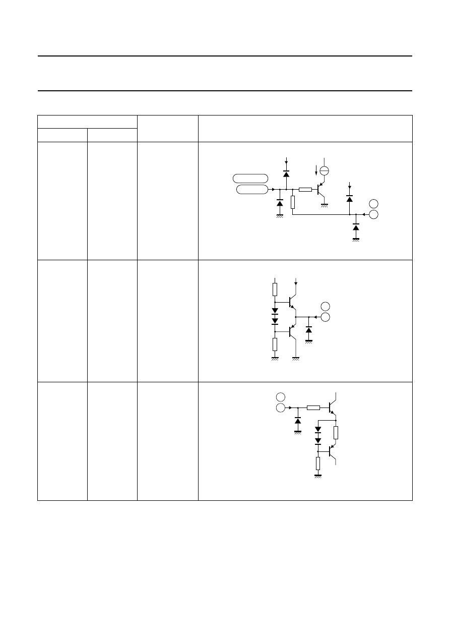
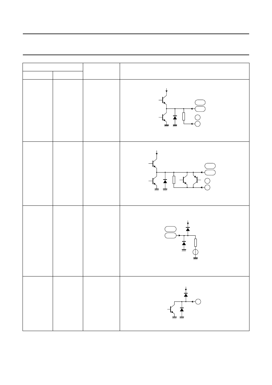
INTERNAL PIN CONFIGURATIONS
PIN
NAME
EQUIVALENT CIRCUIT
TDA1564TH
TDA1564J
17, 18, 13, 14
and 19
1, 2, 16, 17
and 3
IN1+, IN1
−
, IN2
−
,
IN2+ and CIN
16
4
CSE
2
6
MODE
MGR182
1, 2, 16, 17
17, 18, 13, 14
3
19
VP1, VP2
VP1, VP2
J
MGW261
4
16
VP2
J
TH
MGW262
6
2
J
TH
2004 Jan 27
23
Philips Semiconductors
Preliminary specification
High efficiency 2
×
25 W/4
Ω
stereo car radio power amplifier
TDA1564
3, 8
7, 11
OUT1
−
, OUT2+
4, 7
8, 10
OUT1+, OUT2
−
9, 12
12, 14
OC1, OC2
15
15
DIAG
PIN
NAME
EQUIVALENT CIRCUIT
TDA1564TH
TDA1564J
MGR185
4
VP1, VP2
7, 11
16
3, 8
J
J
TH
TH
MGR186
4
VP1, VP2
8, 10
16
4, 7
J
J
TH
TH
MGW263
VP2
12, 14
9, 12
J
TH
MGW264
VP2
15
2004 Jan 27
24
Philips Semiconductors
Preliminary specification
High efficiency 2
×
25 W/4
Ω
stereo car radio power amplifier
TDA1564
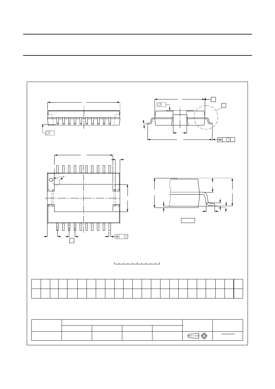
PACKAGE OUTLINES
UNIT
A4
(1)
REFERENCES
OUTLINE
VERSION
EUROPEAN
PROJECTION
ISSUE DATE
IEC
JEDEC
JEITA
mm
+
0.08
−
0.04
3.5
0.35
DIMENSIONS (mm are the original dimensions)
Notes
1. Limits per individual lead.
2. Plastic or metal protrusions of 0.25 mm maximum per side are not included.
SOT418-3
0
5
10 mm
scale
HSOP20: plastic, heatsink small outline package; 20 leads; low stand-off height
SOT418-3
A
max.
detail X
A2
3.5
3.2
D2
1.1
0.9
HE
14.5
13.9
Lp
1.1
0.8
Q
1.7
1.5
2.5
2.0
v
0.25
w
0.25
y
Z
8
°
0
°
θ
0.07
x
0.03
D1
13.0
12.6
E1
6.2
5.8
E2
2.9
2.5
bp
c
0.32
0.23
e
1.27
D
(2)
16.0
15.8
E
(2)
11.1
10.9
0.53
0.40
A3
A4
A2
(A3)
Lp
θ
A
Q
D
y
x
HE
E
c
v
M
A
X
A
bp
w
M
Z
D1
D2
E2
E1
e
20
11
1
10
pin 1 index
02-02-12
03-07-23
2004 Jan 27
25
Philips Semiconductors
Preliminary specification
High efficiency 2
×
25 W/4
Ω
stereo car radio power amplifier
TDA1564
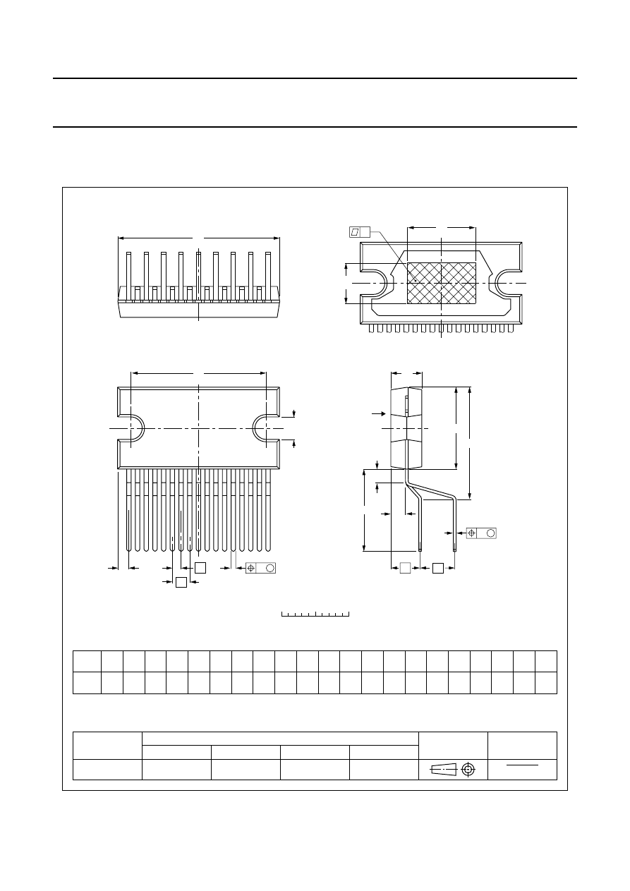
REFERENCES
OUTLINE
VERSION
EUROPEAN
PROJECTION
ISSUE DATE
IEC
JEDEC
JEITA
DIMENSIONS (mm are the original dimensions)
Note
1. Plastic or metal protrusions of 0.25 mm maximum per side are not included.
SOT243-1
0
5
10 mm
scale
D
L
E
A
c
A
2
L
3
Q
w
M
b
p
1
d
D
Z
e
e
x
h
1
17
j
Eh
non-concave
99-12-17
03-03-12
DBS17P: plastic DIL-bent-SIL power package; 17 leads (lead length 12 mm)
SOT243-1
view B: mounting base side
m
2
e
v
M
B
UNIT
A
e
1
A
2
b
p
c
D
(1)
E
(1)
Z
(1)
d
e
D
h
L
L
3
m
mm
17.0
15.5
4.6
4.4
0.75
0.60
0.48
0.38
24.0
23.6
20.0
19.6
10
2.54
v
0.8
12.2
11.8
1.27
e
2
5.08
2.4
1.6
E
h
6
2.00
1.45
2.1
1.8
3.4
3.1
4.3
12.4
11.0
Q
j
0.4
w
0.03
x

2004 Jan 27
26
Philips Semiconductors
Preliminary specification
High efficiency 2
×
25 W/4
Ω
stereo car radio power amplifier
TDA1564
SOLDERING
Introduction
This text gives a very brief insight to a complex technology.
A more in-depth account of soldering ICs can be found in
our
“Data Handbook IC26; Integrated Circuit Packages”
(document order number 9398 652 90011).
There is no soldering method that is ideal for all IC
packages. Wave soldering is often preferred when
through-hole and surface mount components are mixed on
one printed-circuit board. Wave soldering can still be used
for certain surface mount ICs, but it is not suitable for fine
pitch SMDs. In these situations reflow soldering is
recommended. Driven by legislation and environmental
forces the worldwide use of lead-free solder pastes is
increasing.
Through-hole mount packages
S
OLDERING BY DIPPING OR BY SOLDER WAVE
Typical dwell time of the leads in the wave ranges from
3 to 4 seconds at 250
°
C or 265
°
C, depending on solder
material applied, SnPb or Pb-free respectively.
The total contact time of successive solder waves must not
exceed 5 seconds.
The device may be mounted up to the seating plane, but
the temperature of the plastic body must not exceed the
specified maximum storage temperature (T
stg(max)
). If the
printed-circuit board has been pre-heated, forced cooling
may be necessary immediately after soldering to keep the
temperature within the permissible limit.
M
ANUAL SOLDERING
Apply the soldering iron (24 V or less) to the lead(s) of the
package, either below the seating plane or not more than
2 mm above it. If the temperature of the soldering iron bit
is less than 300
°
C it may remain in contact for up to
10 seconds. If the bit temperature is between
300 and 400
°
C, contact may be up to 5 seconds.
Surface mount packages
R
EFLOW SOLDERING
Reflow soldering requires solder paste (a suspension of
fine solder particles, flux and binding agent) to be applied
to the printed-circuit board by screen printing, stencilling or
pressure-syringe dispensing before package placement.
Several methods exist for reflowing; for example,
convection or convection/infrared heating in a conveyor
type oven. Throughput times (preheating, soldering and
cooling) vary between 100 and 200 seconds depending
on heating method.
Typical reflow peak temperatures range from
215 to 270
°
C depending on solder paste material. The
top-surface temperature of the packages should
preferably be kept:
•
below 225
°
C (SnPb process) or below 245
°
C (Pb-free
process)
– for all the BGA, HTSSON..T and SSOP-T packages
– for packages with a thickness
≥
2.5 mm
– for packages with a thickness < 2.5 mm and a
volume
≥
350 mm
3
so called thick/large packages.
•
below 240
°
C (SnPb process) or below 260
°
C (Pb-free
process) for packages with a thickness < 2.5 mm and a
volume < 350 mm
3
so called small/thin packages.
Moisture sensitivity precautions, as indicated on packing,
must be respected at all times.
W
AVE SOLDERING
Conventional single wave soldering is not recommended
for surface mount devices (SMDs) or printed-circuit boards
with a high component density, as solder bridging and
non-wetting can present major problems.
To overcome these problems the double-wave soldering
method was specifically developed.
If wave soldering is used the following conditions must be
observed for optimal results:
•
Use a double-wave soldering method comprising a
turbulent wave with high upward pressure followed by a
smooth laminar wave.
•
For packages with leads on two sides and a pitch (e):
– larger than or equal to 1.27 mm, the footprint
longitudinal axis is preferred to be parallel to the
transport direction of the printed-circuit board;
– smaller than 1.27 mm, the footprint longitudinal axis
must be parallel to the transport direction of the
printed-circuit board.
The footprint must incorporate solder thieves at the
downstream end.
•
For packages with leads on four sides, the footprint must
be placed at a 45
°
angle to the transport direction of the
printed-circuit board. The footprint must incorporate
solder thieves downstream and at the side corners.
During placement and before soldering, the package must
be fixed with a droplet of adhesive. The adhesive can be

2004 Jan 27
27
Philips Semiconductors
Preliminary specification
High efficiency 2
×
25 W/4
Ω
stereo car radio power amplifier
TDA1564
applied by screen printing, pin transfer or syringe dispensing. The package can be soldered after the adhesive is cured.
Typical dwell time of the leads in the wave ranges from 3 to 4 seconds at 250
°
C or 265
°
C, depending on solder material
applied, SnPb or Pb-free respectively.
A mildly-activated flux will eliminate the need for removal of corrosive residues in most applications.
M
ANUAL SOLDERING
Fix the component by first soldering two diagonally-opposite end leads. Use a low voltage (24 V or less) soldering iron
applied to the flat part of the lead. Contact time must be limited to 10 seconds at up to 300
°
C. When using a dedicated
tool, all other leads can be soldered in one operation within 2 to 5 seconds between 270 and 320
°
C.
Suitability of IC packages for wave, reflow and dipping soldering methods
Notes
1. For more detailed information on the BGA packages refer to the
“(LF)BGA Application Note” (AN01026); order a copy
from your Philips Semiconductors sales office.
2. All surface mount (SMD) packages are moisture sensitive. Depending upon the moisture content, the maximum
temperature (with respect to time) and body size of the package, there is a risk that internal or external package
cracks may occur due to vaporization of the moisture in them (the so called popcorn effect). For details, refer to the
Drypack information in the
“Data Handbook IC26; Integrated Circuit Packages; Section: Packing Methods”.
3. For SDIP packages, the longitudinal axis must be parallel to the transport direction of the printed-circuit board.
4. Hot bar soldering or manual soldering is suitable for PMFP packages.
5. These transparent plastic packages are extremely sensitive to reflow soldering conditions and must on no account
be processed through more than one soldering cycle or subjected to infrared reflow soldering with peak temperature
exceeding 217
°
C
±
10
°
C measured in the atmosphere of the reflow oven. The package body peak temperature
must be kept as low as possible.
6. These packages are not suitable for wave soldering. On versions with the heatsink on the bottom side, the solder
cannot penetrate between the printed-circuit board and the heatsink. On versions with the heatsink on the top side,
the solder might be deposited on the heatsink surface.
7. If wave soldering is considered, then the package must be placed at a 45
°
angle to the solder wave direction.
The package footprint must incorporate solder thieves downstream and at the side corners.
MOUNTING
PACKAGE
SOLDERING METHOD
WAVE
REFLOW
DIPPING
Through-hole mount CPGA, HCPGA
suitable
−
suitable
DBS, DIP, HDIP, RDBS, SDIP, SIL
suitable
−
−
Through-hole-
surface mount
not suitable
not suitable
−
Surface mount
SSOP-T
, TFBGA, USON, VFBGA
not suitable
suitable
−
DHVQFN, HBCC, HBGA, HLQFP, HSO,
HSOP, HSQFP, HSSON, HTQFP, HTSSOP,
HVQFN, HVSON, SMS
not suitable
suitable
−
PLCC
, SO, SOJ
suitable
suitable
−
LQFP, QFP, TQFP
not recommended
suitable
−
SSOP, TSSOP, VSO, VSSOP
not recommended
suitable
−
CWQCCN..L
not suitable
not suitable
−

2004 Jan 27
28
Philips Semiconductors
Preliminary specification
High efficiency 2
×
25 W/4
Ω
stereo car radio power amplifier
TDA1564
8. Wave soldering is suitable for LQFP, QFP and TQFP packages with a pitch (e) larger than 0.8 mm; it is definitely not
suitable for packages with a pitch (e) equal to or smaller than 0.65 mm.
9. Wave soldering is suitable for SSOP, TSSOP, VSO and VSSOP packages with a pitch (e) equal to or larger than
0.65 mm; it is definitely not suitable for packages with a pitch (e) equal to or smaller than 0.5 mm.
10. Hot bar or manual soldering is suitable for PMFP packages.
11. Image sensor packages in principle should not be soldered. They are mounted in sockets or delivered pre-mounted
on flex foil. However, the image sensor package can be mounted by the client on a flex foil by using a hot bar
soldering process. The appropriate soldering profile can be provided on request.

2004 Jan 27
29
Philips Semiconductors
Preliminary specification
High efficiency 2
×
25 W/4
Ω
stereo car radio power amplifier
TDA1564
DATA SHEET STATUS
Notes
1. Please consult the most recently issued data sheet before initiating or completing a design.
2. The product status of the device(s) described in this data sheet may have changed since this data sheet was
published. The latest information is available on the Internet at URL http://www.semiconductors.philips.com.
3. For data sheets describing multiple type numbers, the highest-level product status determines the data sheet status.
LEVEL
DATA SHEET
STATUS
PRODUCT
STATUS
DEFINITION
I
Objective data
Development
This data sheet contains data from the objective specification for product
development. Philips Semiconductors reserves the right to change the
specification in any manner without notice.
II
Preliminary data Qualification
This data sheet contains data from the preliminary specification.
Supplementary data will be published at a later date. Philips
Semiconductors reserves the right to change the specification without
notice, in order to improve the design and supply the best possible
product.
III
Product data
Production
This data sheet contains data from the product specification. Philips
Semiconductors reserves the right to make changes at any time in order
to improve the design, manufacturing and supply. Relevant changes will
be communicated via a Customer Product/Process Change Notification
(CPCN).
DEFINITIONS
Short-form specification
The data in a short-form
specification is extracted from a full data sheet with the
same type number and title. For detailed information see
the relevant data sheet or data handbook.
Limiting values definition
Limiting values given are in
accordance with the Absolute Maximum Rating System
(IEC 60134). Stress above one or more of the limiting
values may cause permanent damage to the device.
These are stress ratings only and operation of the device
at these or at any other conditions above those given in the
Characteristics sections of the specification is not implied.
Exposure to limiting values for extended periods may
affect device reliability.
Application information
Applications that are
described herein for any of these products are for
illustrative purposes only. Philips Semiconductors make
no representation or warranty that such applications will be
suitable for the specified use without further testing or
modification.
DISCLAIMERS
Life support applications
These products are not
designed for use in life support appliances, devices, or
systems where malfunction of these products can
reasonably be expected to result in personal injury. Philips
Semiconductors customers using or selling these products
for use in such applications do so at their own risk and
agree to fully indemnify Philips Semiconductors for any
damages resulting from such application.
Right to make changes
Philips Semiconductors
reserves the right to make changes in the products -
including circuits, standard cells, and/or software -
described or contained herein in order to improve design
and/or performance. When the product is in full production
(status ‘Production’), relevant changes will be
communicated via a Customer Product/Process Change
Notification (CPCN). Philips Semiconductors assumes no
responsibility or liability for the use of any of these
products, conveys no licence or title under any patent,
copyright, or mask work right to these products, and
makes no representations or warranties that these
products are free from patent, copyright, or mask work
right infringement, unless otherwise specified.

© Koninklijke Philips Electronics N.V. 2004
SCA76
All rights are reserved. Reproduction in whole or in part is prohibited without the prior written consent of the copyright owner.
The information presented in this document does not form part of any quotation or contract, is believed to be accurate and reliable and may be changed
without notice. No liability will be accepted by the publisher for any consequence of its use. Publication thereof does not convey nor imply any license
under patent- or other industrial or intellectual property rights.
Philips Semiconductors – a worldwide company
Contact information
For additional information please visit http://www.semiconductors.philips.com.
Fax: +31 40 27 24825
For sales offices addresses send e-mail to: sales.addresses@www.semiconductors.philips.com.
Printed in The Netherlands
R32/04/pp
30
Date of release:
2004 Jan 27
Document order number:
9397 750 12613
Document Outline
- Features
- General description
- Quick reference data
- Ordering information
- Block diagram
- Pinning
- Functional description
- Limiting values
- Thermal characteristics
- DC characteristics
- AC characteristics
- Test and application information
- Application notes
- Internal pin configurations
- Package outlines
- Soldering
- Data sheet status
- Definitions
- Disclaimers
Wyszukiwarka
Podobne podstrony:
TDA1563Q Philips elenota pl
TDA1565TH Philips elenota pl
TDA8920 Philips elenota pl
TDA8580 Philips elenota pl
TDA1517 Philips elenota pl
TDA8942P Philips elenota pl
TDA1520 Philips elenota pl
TDA8569Q Philips elenota pl
TDA8574 Philips elenota pl
TDA8924 Philips elenota pl
TDA8922 Philips elenota pl
TDA8510J Philips elenota pl (1)
TDA8552T Philips elenota pl
TDA8567Q Philips elenota pl
TDA8943SF Philips elenota pl
TDA8576T Philips elenota pl
TDA8926 Philips elenota pl
TDA8947J Philips elenota pl
więcej podobnych podstron