
DATA SHEET
Product specification
Supersedes data of 1997 Mar 27
2003 Aug 08
INTEGRATED CIRCUITS
TDA8569Q
4
×
40 W BTL quad car radio
power amplifier

2003 Aug 08
2
Philips Semiconductors
Product specification
4
×
40 W BTL quad car radio
power amplifier
TDA8569Q
FEATURES
•
Capable of driving 2
Ω
loads
•
Requires very few external components
•
High output power
•
Low output offset voltage
•
Fixed gain
•
Diagnostic facility (distortion, short-circuit and
temperature pre-warning)
•
Good ripple rejection
•
Mode select switch (operating, mute and standby)
•
Load dump protection
•
Short-circuit safe to ground, to V
P
and across the load
•
Low power dissipation in any short-circuit condition
•
Thermally protected
•
Reverse polarity safe
•
Electrostatic discharge protection
•
No switch-on/switch-off plop
•
Flexible leads
•
Low thermal resistance
•
Pin compatible with the TDA8567Q.
GENERAL DESCRIPTION
The TDA8569Q is an integrated class-B output amplifier in
a 23-lead Single-In-Line (SIL) plastic power package.
It contains four amplifiers in Bridge-Tied Load (BTL)
configuration, each with a gain of 26 dB. The output power
is 4
×
40 W in a 2
Ω
load.
APPLICATIONS
•
The device is developed primarily for car radio
applications.
QUICK REFERENCE DATA
ORDERING INFORMATION
SYMBOL
PARAMETER
CONDITIONS
MIN.
TYP.
MAX.
UNIT
V
P
operating supply voltage
6
14.4
18
V
I
ORM
repetitive peak output current
−
−
7.5
A
I
q(tot)
total quiescent current
−
230
−
mA
I
stb
standby current
−
0.2
10
µ
A
I
sw
switch-on current
−
−
80
µ
A
Z
i
input impedance
25
30
−
k
Ω
P
o
output power
THD = 10%
−
40
−
W
SVRR
supply voltage ripple rejection
R
s
= 0
Ω
−
60
−
dB
α
cs
channel separation
R
s
= 10 k
Ω
−
55
−
dB
G
v
closed loop voltage gain
25
26
27
dB
V
n(o)
noise output voltage
R
s
= 0
Ω
−
−
120
µ
V
TYPE
NUMBER
PACKAGE
NAME
DESCRIPTION
VERSION
TDA8569Q
DBS23P
plastic DIL-bent-SIL power package; 23 leads (straight lead length 3.2 mm)
SOT411-1
2003 Aug 08
3
Philips Semiconductors
Product specification
4
×
40 W BTL quad car radio
power amplifier
TDA8569Q
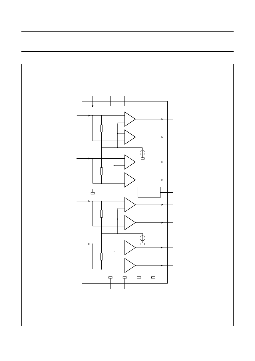
BLOCK DIAGRAM
handbook, full pagewidth
MBK010
OUT1
+
OUT1
−
+
−
+
−
Vref
2
IN1
IN2
4
23
16
8
1
15
10
MODE
VP1
VP2
VP3
VP4
21
18
6
3
PGND1
PGND2
PGND3
PGND4
30 k
Ω
OUT2
+
OUT2
−
+
−
+
−
7
5
11
30 k
Ω
OUT3
+
OUT3
−
+
−
+
−
Vref
17
IN3
SGND
TDA8569Q
IN4
19
13
12
30 k
Ω
OUT4
+
OUT4
−
+
−
+
−
22
20
14
30 k
Ω
VDIAG
DIAGNOSTIC
9
Fig.1 Block diagram.
2003 Aug 08
4
Philips Semiconductors
Product specification
4
×
40 W BTL quad car radio
power amplifier
TDA8569Q
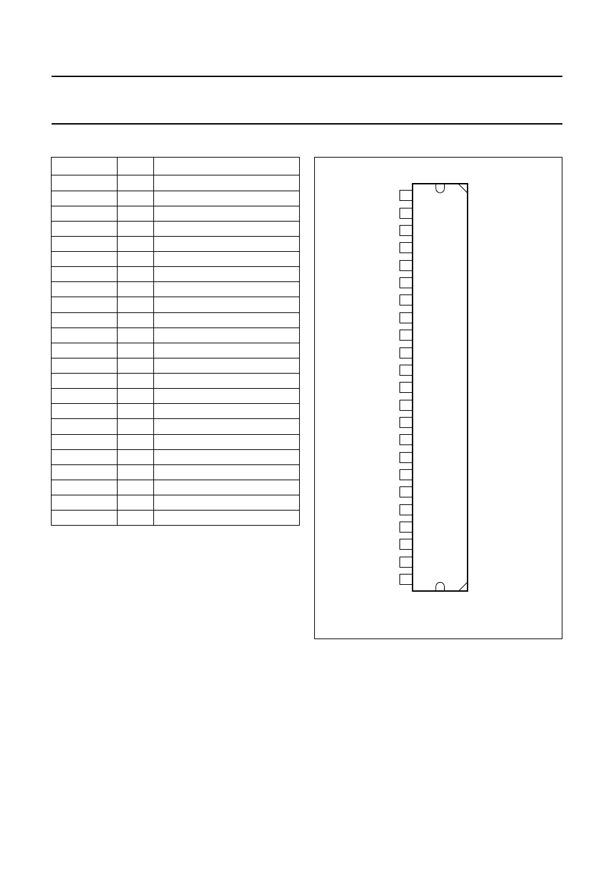
PINNING
SYMBOL
PIN
DESCRIPTION
V
P1
1
supply voltage 1
OUT1+
2
output 1+
PGND1
3
power ground 1
OUT1
−
4
output 1
−
OUT2
−
5
output 2
−
PGND2
6
power ground 2
OUT2+
7
output 2+
V
P2
8
supply voltage 2
V
DIAG
9
diagnostic output
IN1
10
input 1
IN2
11
input 2
SGND
12
signal ground
IN3
13
input 3
IN4
14
input 4
MODE
15
mode select switch input
V
P3
16
supply voltage 3
OUT3+
17
output 3+
PGND3
18
power ground 3
OUT3
−
19
output 3
−
OUT4
−
20
output 4
−
PGND4
21
power ground 4
OUT4+
22
output 4+
V
P4
23
supply voltage 4
handbook, halfpage
TDA8569Q
MBK009
1
2
3
4
5
6
7
8
9
10
11
12
13
14
15
16
17
18
19
20
21
22
23
VP1
OUT1
+
PGND1
OUT1
−
OUT2
−
PGND2
OUT2
+
VP2
VDIAG
IN1
IN2
SGND
IN3
IN4
MODE
VP3
OUT3
+
PGND3
OUT3
−
OUT4
−
PGND4
OUT4
+
VP4
Fig.2 Pin configuration.
2003 Aug 08
5
Philips Semiconductors
Product specification
4
×
40 W BTL quad car radio
power amplifier
TDA8569Q
FUNCTIONAL DESCRIPTION
The TDA8569Q contains four identical amplifiers which
can be used for bridge applications. The gain of each
amplifier is fixed at 26 dB.
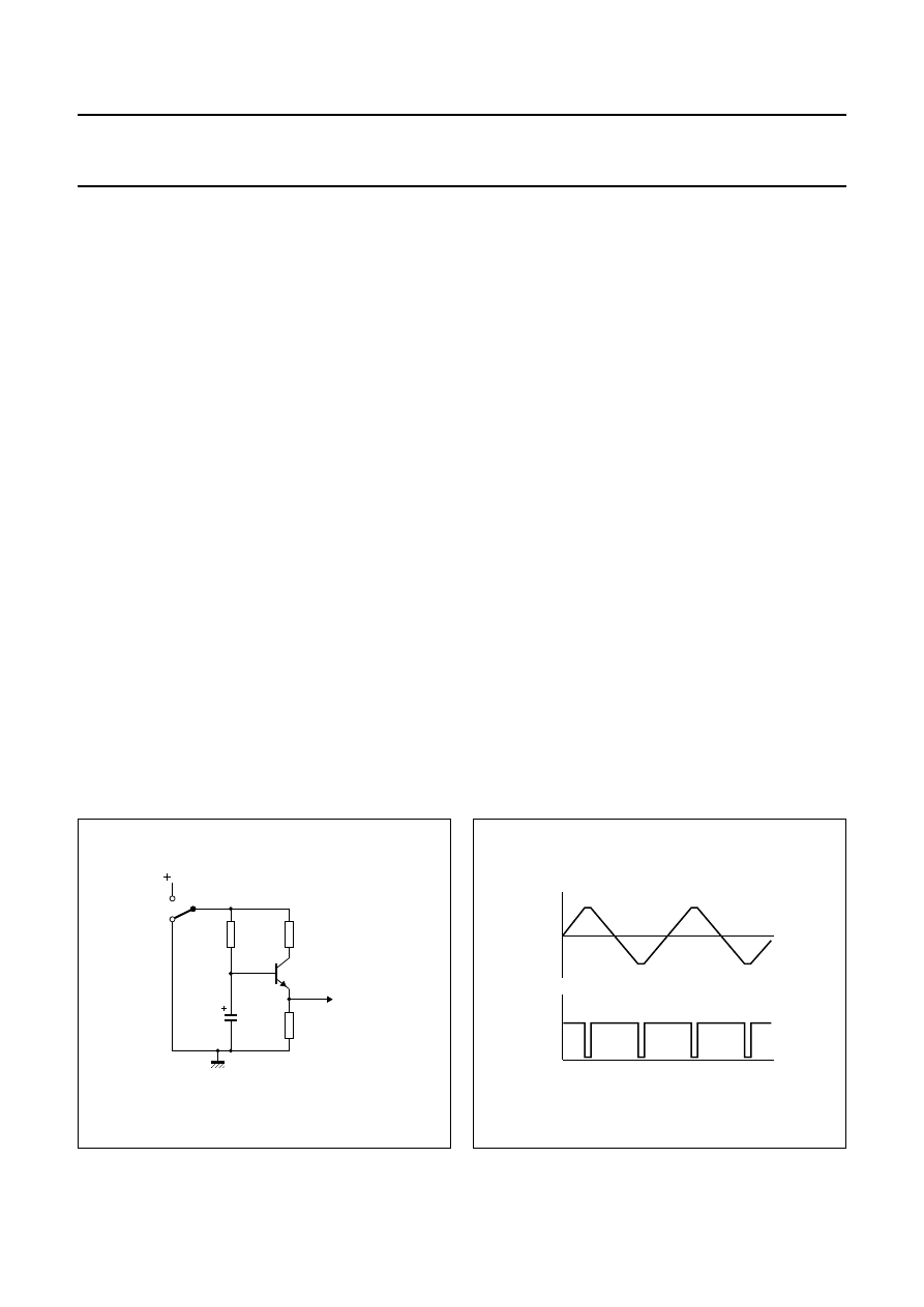
Mode select switch (pin MODE)
•
Standby: low supply current (<100
µ
A)
•
Mute: input signal suppressed
•
Operating: normal on condition.
Since this pin has a low input current (<80
µ
A), a low cost
supply switch can be applied.
To avoid switch-on plops, it is advised to keep the amplifier
in the mute mode during
≥
150 ms (charging of the input
capacitors at pins IN1, IN2, IN3 and IN4).
This can be realized by:
•
Microprocessor control
•
External timing circuit (see Fig.3).
Diagnostic output (pin V
DIAG
)
D
YNAMIC
D
ISTORTION
D
ETECTOR
(DDD)
At the onset of clipping of one or more output stages, the
dynamic distortion detector becomes active and pin V
DIAG
goes LOW. This information can be used to drive a sound
processor or DC volume control to attenuate the input
signal and so limit the distortion. The output level of
pin V
DIAG
is independent of the number of channels that
are clipping (see Fig.4).
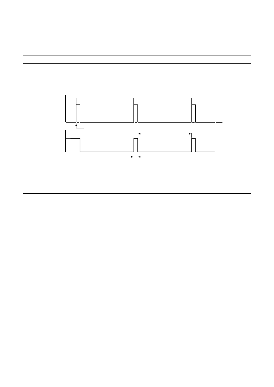
S
HORT
-
CIRCUIT DIAGNOSTIC
When a short-circuit occurs at one or more outputs to
ground or to the supply voltage, the output stages are
switched off until the short-circuit is removed and the
device is switched on again, with a delay of approximately
10 ms after removal of the short-circuit. During this
short-circuit condition, pin V
DIAG
is continuously LOW.
When a short-circuit occurs across the load of one or more
channels, the output stages are switched off for
approximately 10 ms. After that time it is checked during
approximately 50
µ
s to determine whether the short-circuit
is still present. Due to this duty cycle of 50
µ
s/10 ms the
average current consumption during this short-circuit
condition is very low.
During this short-circuit condition, pin V
DIAG
is LOW for
10 ms and HIGH for 50
µ
s (see Fig.5). The protection
circuits of all channels are coupled. This means that if a
short-circuit condition occurs in one of the channels, all
channels are switched off. Consequently, the power
dissipation in any short-circuit condition is very low.
T
EMPERATURE PRE
-
WARNING
When the virtual junction temperature T
vj
reaches 145
°
C,
pin V
DIAG
goes LOW.
O
PEN COLLECTOR OUTPUTS
The diagnostic pin has an open-collector output, so more
devices can be tied together. An external pull-up resistor is
needed.
Fig.3 Mode select switch circuitry.
handbook, halfpage
100 k
Ω
MGA708
47
µ
F
10 k
Ω
100
Ω
mode
select
switch
VP
handbook, halfpage
VDIAG
0
VP
Vo
0
t
MCE461
Fig.4 Distortion detector waveform.
2003 Aug 08
6
Philips Semiconductors
Product specification
4
×
40 W BTL quad car radio
power amplifier
TDA8569Q
handbook, full pagewidth
MCE451
short-circuit over the load
10 ms
50
µ
s
t
t
VP
short
circuit
current
VDIAG
Fig.5 Short-circuit waveform.
2003 Aug 08
7
Philips Semiconductors
Product specification
4
×
40 W BTL quad car radio
power amplifier
TDA8569Q
LIMITING VALUES
In accordance with the Absolute Maximum Rating System (IEC 60134).
THERMAL CHARACTERISTICS
SYMBOL
PARAMETER
CONDITIONS
MIN.
MAX.
UNIT
V
P
supply voltage
operating
−
18
V
non-operating
−
30
V
load dump protection;
during 50 ms; t
r
≥
2.5 ms
−
45
V
V
sc(safe)
short-circuit safe voltage
−
18
V
V
rp
reverse polarity voltage
−
6
V
I
OSM
non-repetitive peak output current
−
10
A
I
ORM
repetitive peak output current
−
7.5
A
P
tot
total power dissipation
−
60
W
T
stg
storage temperature
−
55
+150
°
C
T
amb
ambient temperature
−
40
+85
°
C
T
vj
virtual junction temperature
−
150
°
C
SYMBOL
PARAMETER
VALUE
UNIT
R
th(j-a)
thermal resistance from junction to ambient in free air
40
K/W
R
th(j-c)
thermal resistance from junction to case (see Fig.6)
1
K/W
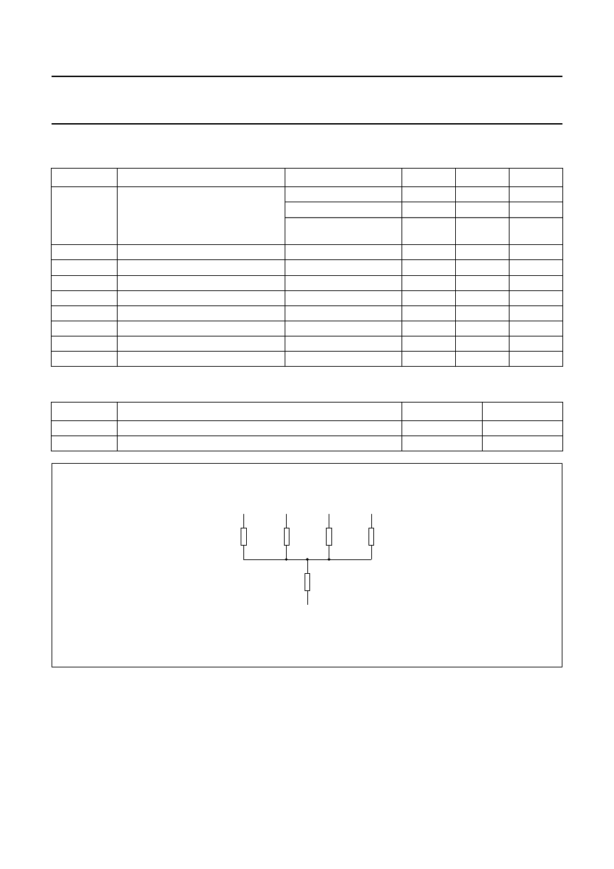
Fig.6 Equivalent thermal resistance network.
handbook, halfpage
3.2 K/W
0.2 K/W
3.2 K/W
3.2 K/W
3.2 K/W
virtual junction
OUT1
OUT2
OUT3
OUT4
case
MGG157

2003 Aug 08
8
Philips Semiconductors
Product specification
4
×
40 W BTL quad car radio
power amplifier
TDA8569Q
DC CHARACTERISTICS
V
P
= 14.4 V; T
amb
= 25
°
C; measured in Fig.7; unless otherwise specified.
Notes
1. The circuit is DC adjusted at V
P
= 6 to 18 V and AC operating at V
P
= 8.5 to 18 V.
2. At V
P
= 18 to 30 V the DC output voltage
≤
1
⁄
2
V
P
.
SYMBOL
PARAMETER
CONDITIONS
MIN.
TYP.
MAX.
UNIT
Supply
V
P
supply voltage
note 1
6
14.4
18
V
I
q(tot)
total quiescent current
R
L
=
∞
−
230
360
mA
Operating condition
V
MODE
mode select switch level
8.5
−
V
P
V
I
MODE
mode select switch current
V
MODE
= 14.4 V
−
30
80
µ
A
V
O
output voltage
note 2
−
7.0
−
V
V
OS
output offset voltage
−
−
150
mV
Mute condition
V
MODE
mode select switch level
3.3
−
6.4
V
V
O
output voltage
note 2
−
7.0
−
V
V
OS
output offset voltage
−
−
100
mV
∆
V
OS
change of output offset voltage
switching between mute and
operating
−
−
100
mV
Standby condition
V
MODE
mode select switch level
0
−
2
V
I
stb
standby current
−
0.2
10
µ
A
Diagnostic
V
DIAG
diagnostic output voltage
during any fault condition
−
−
0.6
V
T
vj
temperature pre-warning
V
DIAG
= 0.6 V
−
145
−
°
C

2003 Aug 08
9
Philips Semiconductors
Product specification
4
×
40 W BTL quad car radio
power amplifier
TDA8569Q
AC CHARACTERISTICS
V
P
= 14.4 V; R
L
= 2
Ω
; f = 1 kHz; T
amb
= 25
°
C; measured in the circuit of Fig.7; unless otherwise specified.
Notes
1. Dynamic Distortion Detector (DDD) active, pin V
DIAG
is set to logic 0.
2. Frequency response externally fixed.
3. V
ripple
= V
ripple(max)
= 2 V (p-p); R
s
= 0
Ω
.
4. B = 20 Hz to 20 kHz; R
s
= 0
Ω
.
5. B = 20 Hz to 20 kHz; R
s
= 10 k
Ω
.
6. B = 20 Hz to 20 kHz; independent of R
s
.
7. P
o
= 25 W; R
s
= 10 k
Ω
.
8. V
i
= V
i(max)
= 1 V (RMS).
SYMBOL
PARAMETER
CONDITIONS
MIN.
TYP.
MAX.
UNIT
P
o
output power
THD = 0.5%
25
30
−
W
THD = 10%
33
40
−
W
V
P
= 13.2 V; THD = 0.5%
−
25
−
W
V
P
= 13.2 V; THD = 10%
−
35
−
W
THD
total harmonic distortion
P
o
= 1 W
−
0.1
−
%
V
DIAG
≤
0.6 V; note 1
−
10
−
%
B
p
power bandwidth
THD = 0.5%; P
o
=
−
1 dB
with respect to 16 W
−
20 to
20000
−
Hz
f
ro(l)
low frequency roll-off
at
−
1 dB; note 2
−
25
−
Hz
f
ro(h)
high frequency roll-off
at
−
1 dB
20
−
−
kHz
G
v
closed loop voltage gain
25
26
27
dB
SVRR
supply voltage ripple rejection on; note 3
50
60
−
dB
mute; note 3
50
60
−
dB
standby; note 3
80
90
−
dB
Z
i
input impedance
25
30
38
k
Ω
V
n(o)
noise output voltage
on; note 4
−
85
120
µ
V
on; note 5
−
100
−
µ
V
mute; note 6
−
60
−
µ
V
α
cs
channel separation
note 7
45
55
−
dB
∆
G
v
channel unbalance
−
−
1
dB
V
o
output signal in mute
note 8
−
−
2
mV
P
o
output power
THD = 0.5%; R
L
= 4
Ω
−
19
−
W
THD = 10%; R
L
= 4
Ω
−
25
−
W
P
o(EIAJ)
EIAJ output power
THD = maximum; square wave
input; V
i
= 2 V (p-p)
−
40
−
W
THD
total harmonic distortion
P
o
= 1 W; R
L
= 4
Ω
−
0.05
−
%
2003 Aug 08
10
Philips Semiconductors
Product specification
4
×
40 W BTL quad car radio
power amplifier
TDA8569Q
TEST AND APPLICATION INFORMATION
handbook, full pagewidth
MBK011
OUT1
+
RL = 2
Ω
OUT1
−
+
−
+
−
Vref
2
IN1
input 1
IN2
input 2
4
15
10
MODE
4700
µ
F
100 nF
23
+
14.4 V
16
8
1
VP1
VP2
VP3
VP4
VP
30 k
Ω
OUT2
+
RL = 2
Ω
OUT2
−
+
−
+
−
7
5
11
30 k
Ω
470 nF
470 nF
470 nF
470 nF
21
18
6
3
PGND1
PGND2
PGND3
PGND4
power ground (substrate)
OUT3
+
RL = 2
Ω
OUT3
−
+
−
+
−
Vref
17
IN3
SGND
TDA8569Q
input 3
IN4
input 4
19
13
12
30 k
Ω
OUT4
+
RL = 2
Ω
OUT4
−
+
−
+
−
22
20
14
30 k
Ω
10 k
Ω
VDIAG
+
VP
DIAGNOSTIC
diagnostic
output
9
Fig.7 Application circuit diagram.
Special care must be taken in the PCB-layout to separate pin V
DIAG
from the pins IN1, IN2, IN3 and IN4 to minimize the crosstalk between the
clip output and the inputs.
To avoid switch-on plops, it is advised to keep the amplifier in the mute mode for a period of
≥
150 ms (charging the input capacitors at
pins IN1, IN2, IN3 and IN4).
2003 Aug 08
11
Philips Semiconductors
Product specification
4
×
40 W BTL quad car radio
power amplifier
TDA8569Q
Test information
Figures 8 to 15 have the following conditions: V
P
= 14.4 V; f = 1 kHz; 80 kHz filter used; unless otherwise specified.
Fig.8 I
P
as a function of V
P
.
handbook, halfpage
0
300
200
100
0
4
VP (V)
IP
(mA)
20
8
12
16
MGD921
R
L
=
∞
.
handbook, halfpage
10
1
f (Hz)
10
−
1
10
−
2
MCE460
10
10
2
10
3
10
4
10
5
THD
+
N
(%)
(1)
(2)
Fig.9 THD + N as a function of frequency.
R
L
= 2
Ω
.
(1) P
o
= 10 W.
(2) P
o
= 1 W.
handbook, halfpage
MCE450
10
−
1
1
10
10
2
Po (W)
10
1
10
−
1
THD
+
N
(%)
10
2
10
−
2
(1)
(2)
(3)
R
L
= 2
Ω
.
(1) f = 10 kHz.
(2) f = 1 kHz.
(3) f = 100 Hz.
Fig.10 THD + N as a function of P
o
.
handbook, halfpage
VP (V)
Po
(W)
10
12
14
16
60
20
0
40
MCE449
(1)
(2)
Fig.11 P
o
as a function of V
P
.
R
L
= 2
Ω
.
(1) THD = 10%.
(2) THD = 0.5%.
2003 Aug 08
12
Philips Semiconductors
Product specification
4
×
40 W BTL quad car radio
power amplifier
TDA8569Q
Fig.12 THD + N as a function of P
o
.
handbook, halfpage
10
1
Po (W)
10
−
1
10
−
2
MBK008
10
−
1
10
−
2
1
10
10
2
THD
+
N
(%)
(1)
(2)
(3)
R
L
= 4
Ω
.
(1) f = 10 kHz.
(2) f = 1 kHz.
(3) f = 100 Hz.
Fig.13 P
o
as a function of V
P
.
R
L
= 4
Ω
.
(1) EIAJ.
(2) THD = 10%.
(3) THD = 0.5%.
handbook, halfpage
8
18
60
0
(1)
(2)
(3)
20
40
10
Po
(W)
VP (V)
12
14
16
MGD922
Fig.14 SVRR as a function of frequency.
handbook, halfpage
−
90
−
70
−
50
−
30
MGD925
10
f (Hz)
SVRR
(dB)
10
2
10
3
10
4
10
5
R
L
= 4
Ω
.
Fig.15 Channel separation as a function of
frequency.
R
L
= 4
Ω
.
(1) channel 1
⇔
channel 2, channel 3
⇔
channel 4.
(2) channels 1 and 2
⇔
channels 3 and 4.
handbook, halfpage
−
90
−
70
−
50
−
30
MGD926
10
(1)
(2)
f (Hz)
α
cs
(dB)
10
2
10
3
10
4
10
5
2003 Aug 08
13
Philips Semiconductors
Product specification
4
×
40 W BTL quad car radio
power amplifier
TDA8569Q
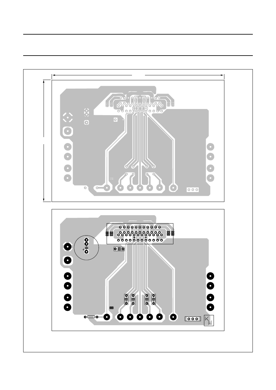
PCB layout
handbook, full pagewidth
MGK079
Pgnd
2200
µ
F
100 nF
470 nF
10 k
Ω
diag
in
1
2
3
4
in
mode
out 4
out 3
sgnd
470 nF
out1
out2
VP
−
+
−
+
−
+
−
+
−
78.74
111.76
Fig.16 PCB layout (component side).
Dimensions in mm.
2003 Aug 08
14
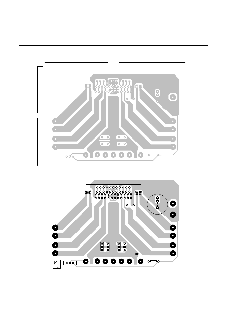
Philips Semiconductors
Product specification
4
×
40 W BTL quad car radio
power amplifier
TDA8569Q
handbook, full pagewidth
MGK080
Pgnd
2200
µ
F
100 nF
470 nF
10 k
Ω
diag
in
1
2
3
4
in
mode
out 4
out 3
sgnd
470 nF
out1
out2
VP
−
+
−
+
−
+
−
+
−
78.74
111.76
Fig.17 PCB layout (soldering side).
Dimensions in mm.
2003 Aug 08
15
Philips Semiconductors
Product specification
4
×
40 W BTL quad car radio
power amplifier
TDA8569Q
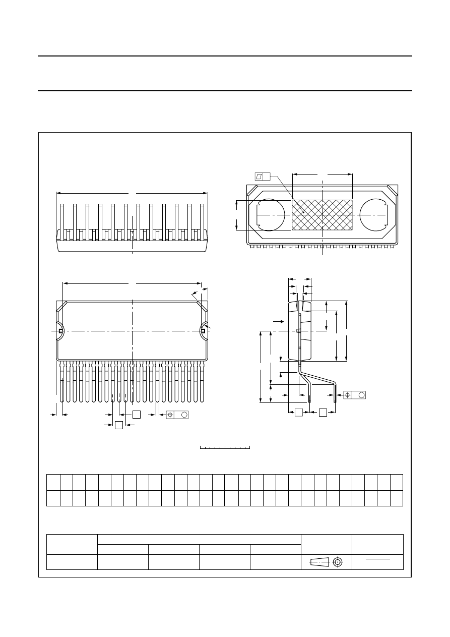
PACKAGE OUTLINE
UNIT A
2
REFERENCES
OUTLINE
VERSION
EUROPEAN
PROJECTION
ISSUE DATE
IEC
JEDEC
JEITA
mm
4.6
4.3
A
4
1.15
0.85
A
5
1.65
1.35
DIMENSIONS (mm are the original dimensions)
Note
1. Plastic or metal protrusions of 0.25 mm maximum per side are not included.
SOT411-1
98-02-20
02-04-24
0
5
10 mm
scale
D
L
L
1
L
2
E
2
E
c
A
4
A
5
A
2
m
L
3
E
1
Q
w
M
b
p
1
d
Z
e
2
e
e
1
23
j
DBS23P: plastic DIL-bent-SIL power package; 23 leads (straight lead length 3.2 mm)
SOT411-1
v
M
D
x
h
Eh
non-concave
view B: mounting base side
B
β
e
1
b
p
c
D
(1)
E
(1)
Z
(1)
d
e
D
h
L
L
3
m
0.75
0.60
0.55
0.35
30.4
29.9
28.0
27.5
12
2.54
12.2
11.8
10.15
9.85
1.27
e
2
5.08
2.4
1.6
E
h
6
E
1
14
13
L
1
10.7
9.9
L
2
6.2
5.8
E
2
1.43
0.78
2.1
1.8
1.85
1.65
4.3
3.6
2.8
Q
j
0.25
w
0.6
v
0.03
x
45
°
β

2003 Aug 08
16
Philips Semiconductors
Product specification
4
×
40 W BTL quad car radio
power amplifier
TDA8569Q
SOLDERING
Introduction to soldering through-hole mount
packages
This text gives a brief insight to wave, dip and manual
soldering. A more in-depth account of soldering ICs can be
found in our
“Data Handbook IC26; Integrated Circuit
Packages” (document order number 9398 652 90011).
Wave soldering is the preferred method for mounting of
through-hole mount IC packages on a printed-circuit
board.
Soldering by dipping or by solder wave
Driven by legislation and environmental forces the
worldwide use of lead-free solder pastes is increasing.
Typical dwell time of the leads in the wave ranges from
3 to 4 seconds at 250
°
C or 265
°
C, depending on solder
material applied, SnPb or Pb-free respectively.
The total contact time of successive solder waves must not
exceed 5 seconds.
The device may be mounted up to the seating plane, but
the temperature of the plastic body must not exceed the
specified maximum storage temperature (T
stg(max)
). If the
printed-circuit board has been pre-heated, forced cooling
may be necessary immediately after soldering to keep the
temperature within the permissible limit.
Manual soldering
Apply the soldering iron (24 V or less) to the lead(s) of the
package, either below the seating plane or not more than
2 mm above it. If the temperature of the soldering iron bit
is less than 300
°
C it may remain in contact for up to
10 seconds. If the bit temperature is between
300 and 400
°
C, contact may be up to 5 seconds.
Suitability of through-hole mount IC packages for dipping and wave soldering methods
Note
1. For SDIP packages, the longitudinal axis must be parallel to the transport direction of the printed-circuit board.
PACKAGE
SOLDERING METHOD
DIPPING
WAVE
DBS, DIP, HDIP, SDIP, SIL
suitable
suitable
(1)

2003 Aug 08
17
Philips Semiconductors
Product specification
4
×
40 W BTL quad car radio
power amplifier
TDA8569Q
DATA SHEET STATUS
Notes
1. Please consult the most recently issued data sheet before initiating or completing a design.
2. The product status of the device(s) described in this data sheet may have changed since this data sheet was
published. The latest information is available on the Internet at URL http://www.semiconductors.philips.com.
3. For data sheets describing multiple type numbers, the highest-level product status determines the data sheet status.
LEVEL
DATA SHEET
STATUS
(1)
PRODUCT
STATUS
(2)(3)
DEFINITION
I
Objective data
Development
This data sheet contains data from the objective specification for product
development. Philips Semiconductors reserves the right to change the
specification in any manner without notice.
II
Preliminary data Qualification
This data sheet contains data from the preliminary specification.
Supplementary data will be published at a later date. Philips
Semiconductors reserves the right to change the specification without
notice, in order to improve the design and supply the best possible
product.
III
Product data
Production
This data sheet contains data from the product specification. Philips
Semiconductors reserves the right to make changes at any time in order
to improve the design, manufacturing and supply. Relevant changes will
be communicated via a Customer Product/Process Change Notification
(CPCN).
DEFINITIONS
Short-form specification
The data in a short-form
specification is extracted from a full data sheet with the
same type number and title. For detailed information see
the relevant data sheet or data handbook.
Limiting values definition
Limiting values given are in
accordance with the Absolute Maximum Rating System
(IEC 60134). Stress above one or more of the limiting
values may cause permanent damage to the device.
These are stress ratings only and operation of the device
at these or at any other conditions above those given in the
Characteristics sections of the specification is not implied.
Exposure to limiting values for extended periods may
affect device reliability.
Application information
Applications that are
described herein for any of these products are for
illustrative purposes only. Philips Semiconductors make
no representation or warranty that such applications will be
suitable for the specified use without further testing or
modification.
DISCLAIMERS
Life support applications
These products are not
designed for use in life support appliances, devices, or
systems where malfunction of these products can
reasonably be expected to result in personal injury. Philips
Semiconductors customers using or selling these products
for use in such applications do so at their own risk and
agree to fully indemnify Philips Semiconductors for any
damages resulting from such application.
Right to make changes
Philips Semiconductors
reserves the right to make changes in the products -
including circuits, standard cells, and/or software -
described or contained herein in order to improve design
and/or performance. When the product is in full production
(status ‘Production’), relevant changes will be
communicated via a Customer Product/Process Change
Notification (CPCN). Philips Semiconductors assumes no
responsibility or liability for the use of any of these
products, conveys no licence or title under any patent,
copyright, or mask work right to these products, and
makes no representations or warranties that these
products are free from patent, copyright, or mask work
right infringement, unless otherwise specified.

© Koninklijke Philips Electronics N.V. 2003
SCA75
All rights are reserved. Reproduction in whole or in part is prohibited without the prior written consent of the copyright owner.
The information presented in this document does not form part of any quotation or contract, is believed to be accurate and reliable and may be changed
without notice. No liability will be accepted by the publisher for any consequence of its use. Publication thereof does not convey nor imply any license
under patent- or other industrial or intellectual property rights.
Philips Semiconductors – a worldwide company
Contact information
For additional information please visit http://www.semiconductors.philips.com.
Fax: +31 40 27 24825
For sales offices addresses send e-mail to: sales.addresses@www.semiconductors.philips.com.
Printed in The Netherlands
753503/02/pp
18
Date of release:
2003 Aug 08
Document order number:
9397 750 11575
Document Outline
- FEATURES
- GENERAL DESCRIPTION
- APPLICATIONS
- QUICK REFERENCE DATA
- ORDERING INFORMATION
- BLOCK DIAGRAM
- PINNING
- FUNCTIONAL DESCRIPTION
- LIMITING VALUES
- THERMAL CHARACTERISTICS
- DC CHARACTERISTICS
- AC CHARACTERISTICS
- TEST AND APPLICATION INFORMATION
- PACKAGE OUTLINE
- SOLDERING
- DATA SHEET STATUS
- DEFINITIONS
- DISCLAIMERS
Wyszukiwarka
Podobne podstrony:
TDA8567Q Philips elenota pl
TDA8566Q Philips elenota pl
TDA8563AQ Philips elenota pl
TDA8566TH Philips elenota pl
TDA8920 Philips elenota pl
TDA8580 Philips elenota pl
TDA1517 Philips elenota pl
TDA8942P Philips elenota pl
TDA1563Q Philips elenota pl
TDA1520 Philips elenota pl
TDA8574 Philips elenota pl
TDA8924 Philips elenota pl
TDA8922 Philips elenota pl
TDA8510J Philips elenota pl (1)
TDA8552T Philips elenota pl
TDA8943SF Philips elenota pl
TDA8576T Philips elenota pl
więcej podobnych podstron