
DATA SHEET
Preliminary specification
File under Integrated Circuits, IC01
1998 Jul 14
INTEGRATED CIRCUITS
TDA1563Q
2
×
25 W high efficiency car radio
power amplifier

1998 Jul 14
2
Philips Semiconductors
Preliminary specification
2
×
25 W high efficiency car radio power
amplifier
TDA1563Q
FEATURES
•
Low dissipation due to switching from Single-Ended
(SE) to Bridge-Tied Load (BTL) mode
•
Differential inputs with high Common Mode Rejection
Ratio (CMRR)
•
Mute/standby/operating (mode select pin)
•
Zero crossing mute circuit
•
Load dump protection circuit
•
Short-circuit safe to ground, to supply voltage and
across load
•
Loudspeaker protection circuit
•
Device switches to single-ended operation at excessive
junction temperature
•
Thermal protection at high junction temperature
(170
°
C)
•
Diagnostic information (clip and protection/prewarning)
•
Clipping information is selectable between
THD = 2.5% or 10%.
GENERAL DESCRIPTION
The TDA1563Q is a monolithic power amplifier in a 17 lead
Single In-Line (SIL) plastic power package. It contains two
identical 25 W amplifiers. The dissipation is minimized by
switching from SE to BTL mode, only when a higher output
voltage swing is needed. The device is primarily
developed for car radio applications.
QUICK REFERENCE DATA
ORDERING INFORMATION
SYMBOL
PARAMETER
CONDITIONS
MIN.
TYP.
MAX.
UNIT
V
P
supply voltage
DC biased
6.0
14.4
18.0
V
non operating
−
−
30
V
load dump
−
−
45
V
I
ORM
repetitive peak output current
−
−
4
A
I
q
quiescent supply current
R
L
=
∞
−
95
150
mA
I
stb
standby current
−
1
50
µ
A
Z
i
input impedance
90
120
150
k
Ω
P
o
output power
R
L
= 4
Ω
; EIAJ
−
38
−
W
R
L
= 4
Ω
; THD = 10%
23
25
−
W
R
L
= 4
Ω
; THD = 2.5%
18
20
−
W
G
v
closed loop voltage gain
P
o
= 1 W
25
26
27
dB
CMRR
common mode rejection ratio
f = 1 kHz; R
s
= 0
Ω
−
80
−
dB
SVRR
supply voltage ripple rejection
f = 1 kHz; R
s
= 0
Ω
45
60
−
dB
∆
V
O
DC output offset voltage
−
−
100
mV
α
cs
channel separation
R
s
= 0
Ω
; P
o
= 15 W
40
60
−
dB
∆
G
v
channel unbalance
−
−
1
dB
TYPE
NUMBER
PACKAGE
NAME
DESCRIPTION
VERSION
TDA1563Q
DBS17P
plastic DIL-bent-SIL power package; 17 leads (lead length 12 mm)
SOT243-1
1998 Jul 14
3
Philips Semiconductors
Preliminary specification
2
×
25 W high efficiency car radio power
amplifier
TDA1563Q
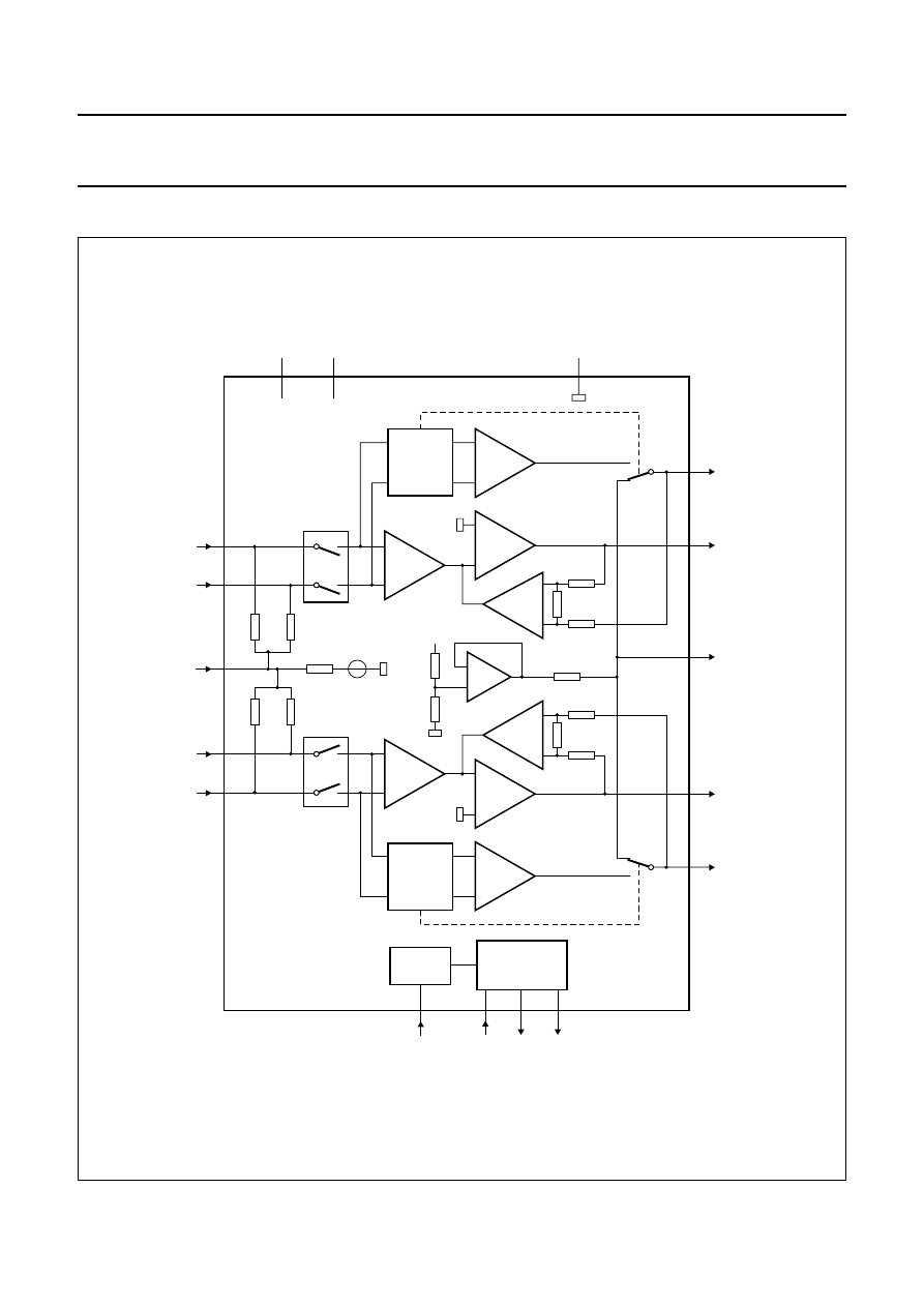
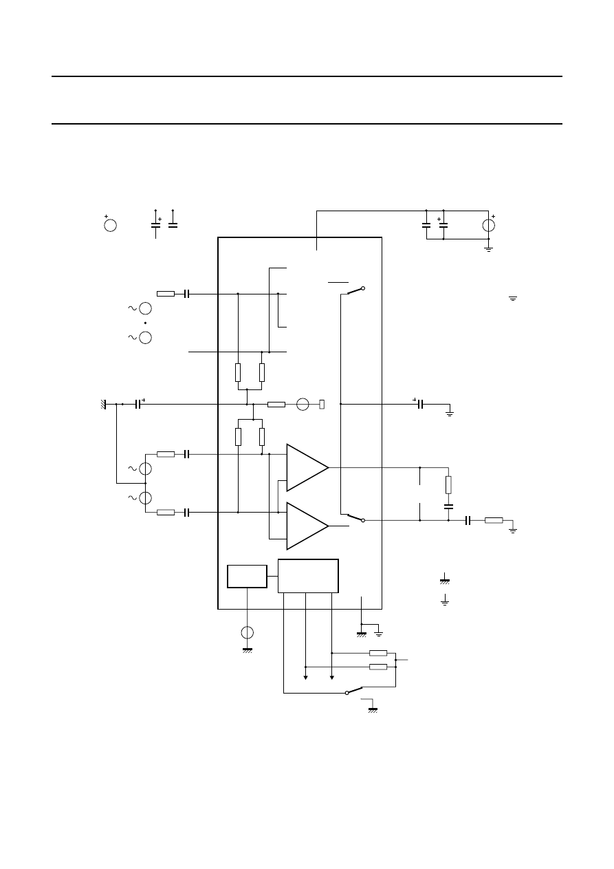
BLOCK DIAGRAM
Fig.1 Block diagram.
handbook, full pagewidth
MGR173
+
−
+
−
+
−
+
−
MUTE
SLAVE
CONTROL
17
16
IN2
+
3
CIN
IN2
−
60
k
Ω
60
k
Ω
60
k
Ω
60
k
Ω
25 k
Ω
Vref
OUT2
−
OUT2
+
10
11
CSE
4
+
−
+
−
+
−
+
−
MUTE
SLAVE
CONTROL
1
2
IN1
+
IN1
−
OUT1
+
OUT1
−
8
7
+
−
VP
STANDBY
LOGIC
CLIP AND
PROTECTION/
PREWARNING
6
12
14
15
MODE
SC
PROT CLIP
GND
9
VP2
13
VP1
5
TDA1563Q
1998 Jul 14
4
Philips Semiconductors
Preliminary specification
2
×
25 W high efficiency car radio power
amplifier
TDA1563Q
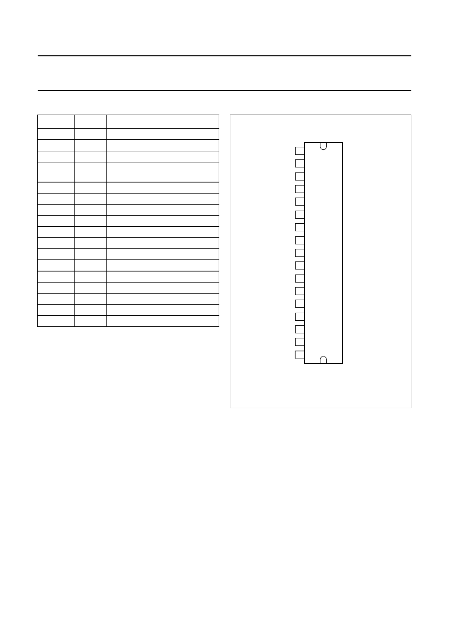
PINNING
SYMBOL
PIN
DESCRIPTION
IN1+
1
non-inverting input 1
IN1
−
2
inverting input 1
CIN
3
common input
C
SE
4
electrolytic capacitor for
Single-Ended (SE) mode
V
P1
5
supply voltage 1
MODE
6
mute/standby/operating
OUT1
−
7
inverting output 1
OUT1+
8
non-inverting output 1
GND
9
ground
OUT2
−
10
inverting output 2
OUT2+
11
non-inverting output 2
SC
12
selectable clip
V
P2
13
supply voltage 2
PROT
14
diagnostic: protection/prewarning
CLIP
15
diagnostic: clip
IN2
−
16
inverting input 2
IN2+
17
non-inverting input 2
Fig.2 Pin configuration.
handbook, halfpage
TDA1563Q
MGR174
IN1
+
IN1
−
CIN
CSE
VP1
MODE
OUT1
−
OUT1
+
GND
OUT2
−
OUT2
+
SC
VP2
PROT
CLIP
IN2
−
IN2
+
1
2
3
4
5
6
7
8
9
10
11
12
13
14
15
16
17

1998 Jul 14
5
Philips Semiconductors
Preliminary specification
2
×
25 W high efficiency car radio power
amplifier
TDA1563Q
FUNCTIONAL DESCRIPTION
The TDA1563Q contains two identical amplifiers with
differential inputs. At low output power (up to output
amplitudes of 3 V (RMS) at V
P
= 14.4 V), the device
operates as a normal SE amplifier. When a larger output
voltage swing is needed, the circuit switches internally to
BTL operation.
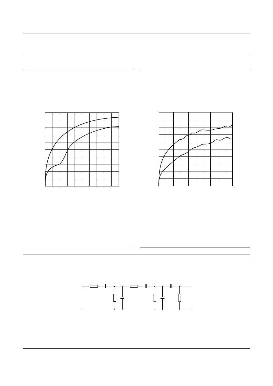
With a sine wave input signal the dissipation of a
conventional BTL amplifier up to 2 W output power is more
than twice the dissipation of the TDA1563Q (see Fig.11).
In normal use, when the amplifier is driven with music-like
signals, the high (BTL) output power is only needed for a
small percentage of time. Under the assumption that a
music signal has a normal (Gaussian) amplitude
distribution, the dissipation of a conventional BTL amplifier
with the same output power is approximately 70% higher
(see Fig.12).
The heatsink has to be designed for use with music
signals. With such a heatsink, the thermal protection will
disable the BTL mode when the junction temperature
exceeds 150
°
C. In this case the output power is limited to
5 W per amplifier.
The gain of each amplifier is internally fixed at 26 dB. With
the MODE pin, the device can be switched to the following
modes:
•
Standby with low standby current (<50
µ
A)
•
Mute condition, DC adjusted
•
On, operation.
The information on pin SC (selectable clip) determines at
which distortion figures a clip signal will be generated at
the clip output. A logic 0 applied to pin SC will select clip
detection at THD = 10%, a logic 1 selects THD = 2.5%.
A logic 0 can be realised by connecting this pin to ground.
A logic 1 can be realised by connecting it to V
logic
(see Fig.8) or the pin can also be left open. This pin may
not be connected to V
p
because it’s maximum input
voltage is 18 V (V
p
> 18 V under load dump conditions).
The device is fully protected against short-circuiting of the
output pins to ground and to the supply voltage. It is also
protected against short-circuiting the loudspeaker and
high junction temperatures. In the event of a permanent
short-circuit condition to ground or the supply voltage, the
output stage will be switched off resulting in a low
dissipation. With permanent short-circuiting of the
loudspeaker, the output stage will be repeatedly switched
on and off. The duty cycle in the ‘on’ condition is low
enough to prevent excessive dissipation.
To avoid plops during switching from ‘mute’ to ‘on’ or from
‘on’ to ‘mute/standby’ while an input signal is present, a
built-in zero-crossing detector allows only switching at
zero input voltage. However, when the supply voltage
drops below 6 V (e.g. engine start), the circuit mutes
immediately avoiding clicks coming from electronic
circuitry preceding the power amplifier.
The voltage on the electrolytic capacitor C
SE
(pin 4) is kept
at 0.5
×
V
P
by means of a voltage buffer (see Fig.1).
The value of this capacitor has an important influence on
the output power in SE mode, especially at low signal
frequencies. A high value is recommended to minimize
dissipation at low frequencies.
The two diagnostic outputs (clip and
protection/prewarning) are open collector outputs and
require a pull-up resistor.
The clip output will be LOW when the THD of the output
signal is higher as the selected clip level (10% or 2.5%).
The protection/prewarning output gives information about:
•
Short-circuit protection:
– When a short-circuit occurs (for at least 50 ms) at the
outputs to ground or the supply voltage, the output
stages are switched off to prevent excessive
dissipation. The outputs will be switched on again
approx. 20 ms after removing the short. During this
short-circuit condition the protection pin will be LOW.
– When a short-circuit occurs across the load, the
output stages are switched off during approx. 20 ms.
After that time a check is performed whether the short
is still present. The power dissipation in any
short-circuit condition is very low.
•
Temperature detection:
– A prewarning indicates the temperature protection
will become active. The prewarning can be used to
reduce the input signal and so reducing the power
dissipation.
1998 Jul 14
6
Philips Semiconductors
Preliminary specification
2
×
25 W high efficiency car radio power
amplifier
TDA1563Q
LIMITING VALUES
In accordance with the Absolute Maximum Rating System (IEC 134).
THERMAL CHARACTERISTICS
Note
1. The value of R
th(c-h)
depends on the application (see Fig.3).
SYMBOL
PARAMETER
CONDITIONS
MIN.
MAX.
UNIT
V
P
supply voltage
operating
−
18
V
non operating
−
30
V
load dump; t
r
> 2.5 ms
−
45
V
V
P(sc)
short-circuit safe voltage
−
18
V
V
rp
reverse polarity voltage
−
6
V
I
ORM
repetitive peak output current
−
4
A
P
tot
total power dissipation
−
60
W
T
stg
storage temperature
−
55
+150
°
C
T
vj
virtual junction temperature
−
150
°
C
T
amb
operating ambient temperature
−
40
−
°
C
SYMBOL
PARAMETER
CONDITIONS
VALUE
UNIT
R
th(j-c)
thermal resistance from junction to case
see note 1
1.3
K/W
R
th(j-a)
thermal resistance from junction to ambient
40
K/W
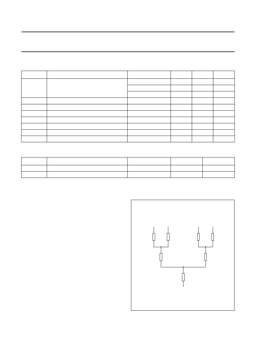
Heatsink design
There are two parameters that determine the size of the
heatsink. The first is the rating for the virtual junction
temperature and the second is the ambient temperature at
which the amplifier must still deliver its full power in the
BTL mode.
With a conventional BTL amplifier, the maximum power
dissipation with a music-like signal (at each amplifier) will
be approximately two times 6.5 W.
At a virtual junction temperature of 150
°
C and a maximum
ambient temperature of 65
°
C, R
th(vj-c)
= 1.3 K/W and
R
th(c-h)
= 0.2 K/W, the thermal resistance of the heatsink
should be:
Compared to a conventional BTL amplifier, the TDA1563Q
has a higher efficiency. The thermal resistance of the
heatsink should be:
150
65
–
2
6.5
×
----------------------
1.3
–
0.2
–
5 K/W
=
1.7
150
65
–
2
6.5
×
----------------------
1.3
–
0.2
–
9.6 K/W
=
Fig.3 Thermal equivalent resistance network.
handbook, halfpage
3.6 K/W
0.6 K/W
3.6 K/W
virtual junction
OUT1
+
OUT1
−
case
3.6 K/W
0.6 K/W
3.6 K/W
OUT2
+
OUT2
−
MGR175
0.1 K/W

1998 Jul 14
7
Philips Semiconductors
Preliminary specification
2
×
25 W high efficiency car radio power
amplifier
TDA1563Q
DC CHARACTERISTICS
V
P
= 14.4 V; T
amb
= 25
°
C; measured in Fig.8; unless otherwise specified.
Notes
1. The circuit is DC biased at V
P
= 6 to 18 V and AC operating at V
P
= 8 to 18 V.
2. If the junction temperature exceeds 150
°
C, the output power is limited to 5 W per channel.
SYMBOL
PARAMETER
CONDITIONS
MIN.
TYP.
MAX.
UNIT
Supplies
V
P
supply voltage
note 1
6.0
14.4
18.0
V
I
q
quiescent supply current
R
L
=
∞
−
95
150
mA
I
stb
standby current
−
1
50
µ
A
V
C
average electrolytic capacitor
voltage at pin 4
−
7.1
−
V
∆
V
O
DC output offset voltage
on state
−
−
100
mV
mute state
−
−
100
mV
Mode select switch (see Fig.4)
V
ms
voltage at mode select pin
(pin 6)
standby condition
0
−
1
V
mute condition
2
−
3
V
on condition
4
5
V
p
V
I
ms
switch current through pin 6
V
ms
= 5 V
−
−
40
µ
A
Diagnostic
V
PROT/CLIP
output voltage at diagnostic
pins: protection/prewarning
(pin 14) and clip (pin 15)
active at logic 0
−
−
0.5
V
I
PROT/CLIP
current through pin 14 or 15
active at logic 0
2
−
−
mA
V
SC
input voltage at selectable clip
pin (pin 12)
logic 0, THD = 10%
−
−
0.5
V
logic 1, THD = 2.5%
1.5
−
18
V
Protection
T
pre
prewarning temperature
−
145
−
°
C
T
dis
BTL disable temperature
note 2
−
150
−
°
C
1998 Jul 14
8
Philips Semiconductors
Preliminary specification
2
×
25 W high efficiency car radio power
amplifier
TDA1563Q
AC CHARACTERISTICS
V
P
= 14.4 V; R
L
= 4
Ω
; C
SE
= 1000
µ
F; f = 1 kHz; T
amb
= 25
°
C; measured in Fig.8; unless otherwise specified.
SYMBOL
PARAMETER
CONDITIONS
MIN.
TYP.
MAX.
UNIT
P
o
output power
THD = 0.5%
15
19
−
W
THD = 10%
23
25
−
W
EIAJ
−
38
−
W
V
P
= 13.2 V; THD = 0.5%
−
16
−
W
V
P
= 13.2 V; THD = 10%
−
20
−
W
THD
total harmonic distortion
P
o
= 1 W; note 1
−
0.1
−
%
P
d
dissipated power
see Figs 11 and 12
W
B
p
power bandwidth
THD = 1%; P
o
=
−
1 dB
with respect to 15 W
−
20 to
15000
−
Hz
f
ro(l)
low frequency roll-off
−
1 dB; note 2
−
25
−
Hz
f
ro(h)
high frequency roll-off
−
1 dB
130
−
−
kHz
G
v
closed loop voltage gain
P
o
= 1 W
25
26
27
dB
SVRR
supply voltage ripple rejection
R
s
= 0
Ω
; V
ripple
= 2 V (p-p)
on
45
60
−
dB
mute
−
90
−
dB
standby; f = 100 Hz to 10 kHz 80
−
−
dB
CMRR
common mode rejection ratio
R
s
= 0
Ω
−
80
−
dB
Z
i
input impedance
90
120
150
k
Ω
∆
Z
i
mismatch in input impedance
−
1
−
%
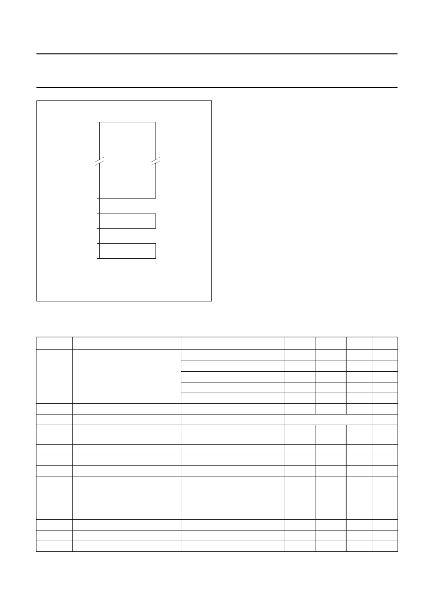
Fig.4 Switching levels of the mode select switch.
handbook, halfpage
,,,,,
,,,,,
,,,,,
,,,,,
,,,,,
,,,,,
MGR176
VP
4
3
2
1
0
,,,,,
,,,,,
,,,,,
,,,,,
Mute
Operating
Standby
,
,
,
,
,
,
1998 Jul 14
9
Philips Semiconductors
Preliminary specification
2
×
25 W high efficiency car radio power
amplifier
TDA1563Q
Notes
1. The distortion is measured with a bandwidth of 10 Hz to 30 kHz.
2. Frequency response externally fixed (input capacitors determine low frequency roll-off).
3. The SE to BTL switch voltage level depends on V
P
.
4. Noise output voltage measured with a bandwidth of 20 Hz to 20 kHz.
5. Noise output voltage is independent of R
s
.
V
SE-BTL
SE to BTL switch voltage level
note 3
−
3
−
V
V
o(mute)
mute mode output voltage
(RMS value)
V
i
= 1 V (RMS)
−
80
150
µ
V
V
n(o)
noise output voltage
on; R
s
= 0
Ω
; note 4
−
80
150
µ
V
on; R
s
= 10 k
Ω
; note 4
−
85
−
µ
V
mute; note 5
−
80
150
µ
V
α
cs
channel separation
R
s
= 0
Ω
; P
o
= 15 W
40
60
−
dB
∆
G
v
channel unbalance
−
−
1
dB
SYMBOL
PARAMETER
CONDITIONS
MIN.
TYP.
MAX.
UNIT
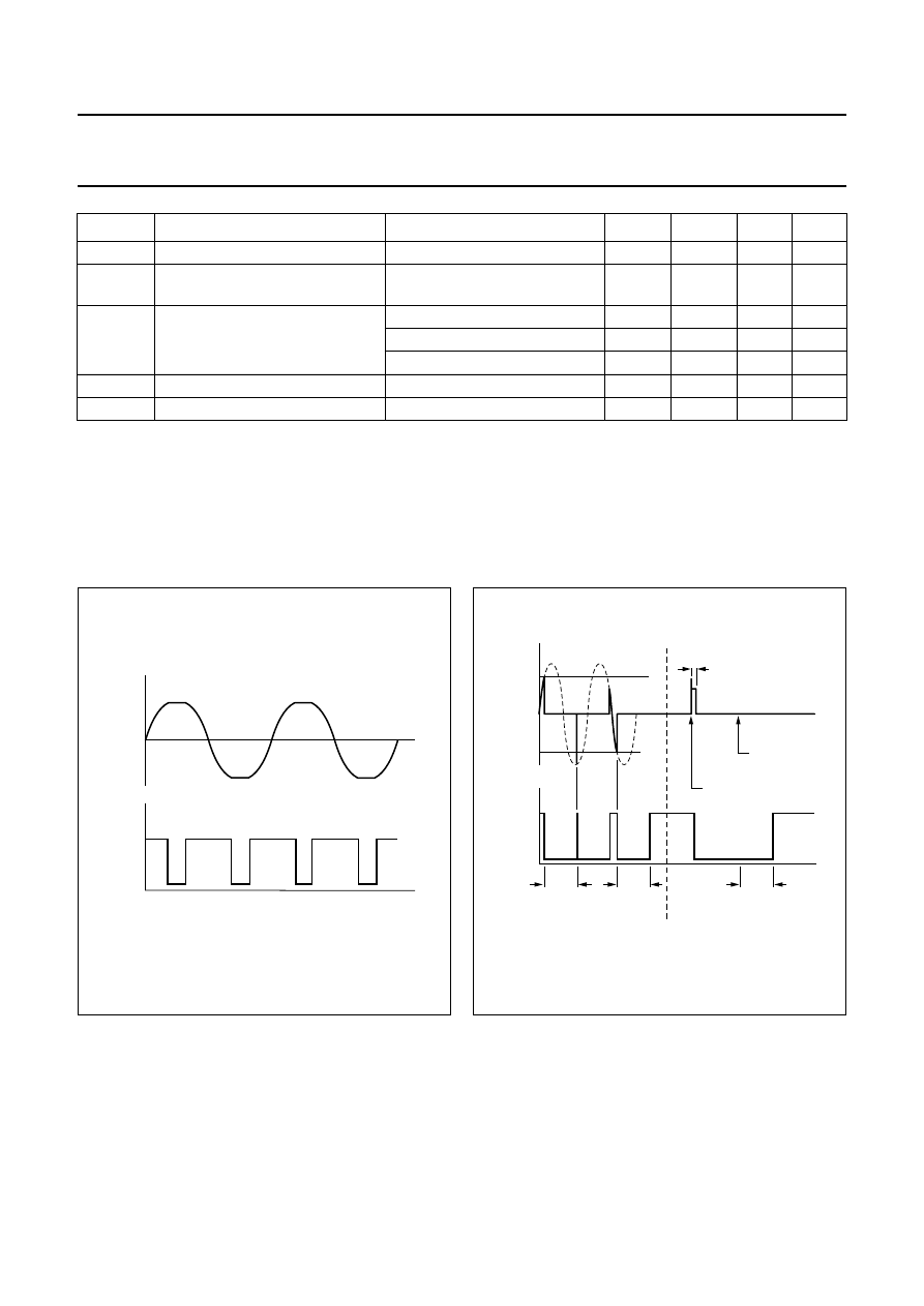
Fig.5 Clip detection waveforms.
handbook, halfpage
MGR177
Vo
VCLIP
0
0
t
Fig.6 Protection waveforms.
handbook, halfpage
MGR178
maximum current
short-circuit to supply pins
short-circuit
to ground
short-circuit
removed
50
ms
50
ms
50
ms
50
µ
s
Io
IPROT
0
max
max
t
t


1998 Jul 14
14
Philips Semiconductors
Preliminary specification
2
×
25 W high efficiency car radio power
amplifier
TDA1563Q
ADDITIONAL APPLICATION INFORMATION
Fig.11 Dissipation; sine wave driven.
Input signal 1 kHz, sinusoidal; V
P
= 14.4 V.
(1) For a conventional BTL amplifier.
(2) For TDA1563Q.
handbook, halfpage
0
10
Po (W)
25
0
5
10
15
20
2
Pd
(W)
4
6
8
MBH692
(1)
(2)
Fig.12 Dissipation; pink noise through IEC-268
filter.
(1) For a conventional BTL amplifier.
(2) For TDA1563Q.
handbook, halfpage
0
10
Po (W)
25
0
5
10
15
20
2
Pd
(W)
4
6
8
MBH693
(1)
(2)
Fig.13 IEC-268 filter.
430
Ω
input
output
330
Ω
3.3
k
Ω
3.3
k
Ω
10
k
Ω
91
nF
68
nF
470 nF
2.2
µ
F
2.2
µ
F
MGC428

1998 Jul 14
15
Philips Semiconductors
Preliminary specification
2
×
25 W high efficiency car radio power
amplifier
TDA1563Q
Fig.14 Test and application diagram for dissipation measurements with a music-like signal (pink noise).
handbook, full pagewidth
1998 Jul 14
16
Philips Semiconductors
Preliminary specification
2
×
25 W high efficiency car radio power
amplifier
TDA1563Q
Fig.15 Quiescent current as a function of V
P
.
V
ms
= 5 V; R
I
=
∞
.
handbook, halfpage
0
150
100
50
0
8
Vp (V)
Iq
(mA)
24
16
MDA845
V
P
= 14.4 V; V
i
= 25 mV.
Fig.16 I
P
as a function of V
ms
(pin 6).
handbook, halfpage
0
2
Vms (V)
Ip
(mA)
4
6
250
0
200
150
100
50
MDA844
Fig.17 Output power as a function of V
P
.
handbook, halfpage
8
18
60
0
20
40
10
Po
(W)
Vp (V)
12
14
16
MDA843
(1)
(2)
(3)
(1) EIAJ, 100 Hz.
(2) THD = 10 %.
(3) THD = 0.5 %.
Fig.18 THD + noise as a function of P
o
.
(1) f = 10 kHz.
(2) f = 1 kHz.
(3) f = 100 Hz.
handbook, halfpage
10
1
10
−
1
10
−
1
10
−
2
10
−
2
MDA842
1
10
THD + N
(%)
10
2
(1)
(2)
(3)
Po (W)
1998 Jul 14
17
Philips Semiconductors
Preliminary specification
2
×
25 W high efficiency car radio power
amplifier
TDA1563Q
Fig.19 THD + noise as a function of frequency.
(1) P
o
= 10 W.
(2) P
o
= 1 W.
handbook, halfpage
10
1
10
−
1
10
−
2
MDA841
10
10
2
10
3
10
4
THD + N
(%)
f (Hz)
10
5
(1)
(2)
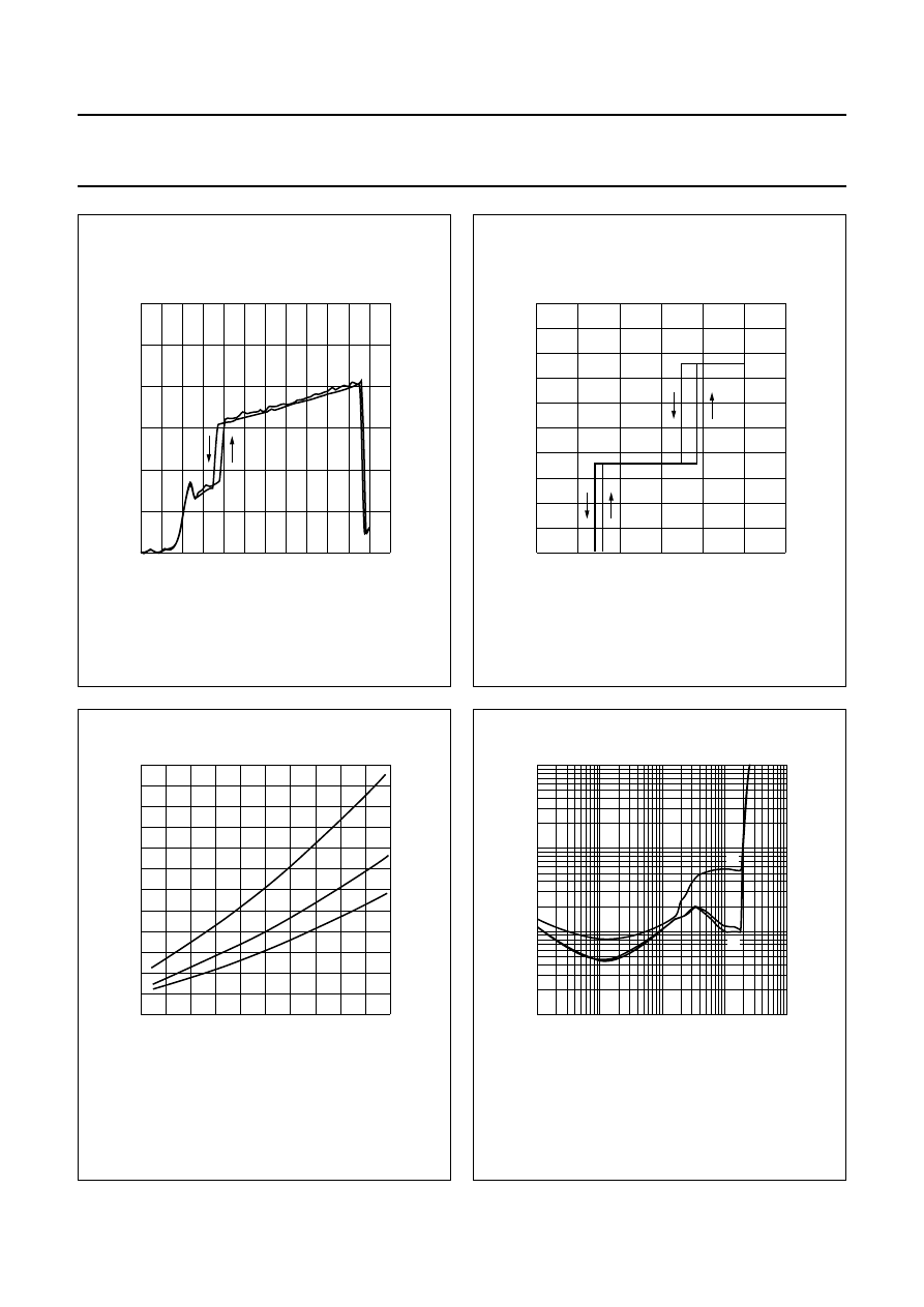
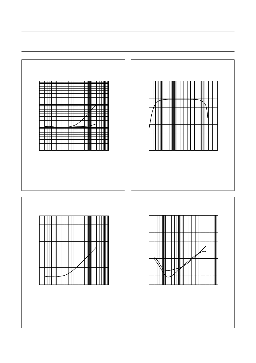
Fig.20 Gain as a function of frequency.
V
i
= 10 mV.
handbook, halfpage
20
22
24
26
Gv
(dB)
f (Hz)
28
MDA840
10
10
2
10
3
10
4
10
5
10
6
Fig.21 SVRR as a function of frequency.
V
ripple(p-p)
= 2 V.
handbook, halfpage
−
80
−
60
−
40
−
20
0
MDA839
10
f (Hz)
SVRR
(dB)
10
2
10
3
10
4
10
5
Fig.22 Channel separation as a function of
frequency.
(1) P
o
= 10 W.
(2) P
o
= 1 W.
handbook, halfpage
−
90
−
70
−
50
−
30
−
10
MDA838
10
f (Hz)
α
cs
(dB)
10
2
10
3
10
4
10
5
(1)
(2)

1998 Jul 14
18
Philips Semiconductors
Preliminary specification
2
×
25 W high efficiency car radio power
amplifier
TDA1563Q
Fig.23 AC operating as a function of V
p
.
handbook, halfpage
0
8
Vp (V)
Po
(W)
24
0.8
0.6
0.2
0
0.4
16
MDA846
V
i
= 10 mV.
1998 Jul 14
19
Philips Semiconductors
Preliminary specification
2
×
25 W high efficiency car radio power
amplifier
TDA1563Q
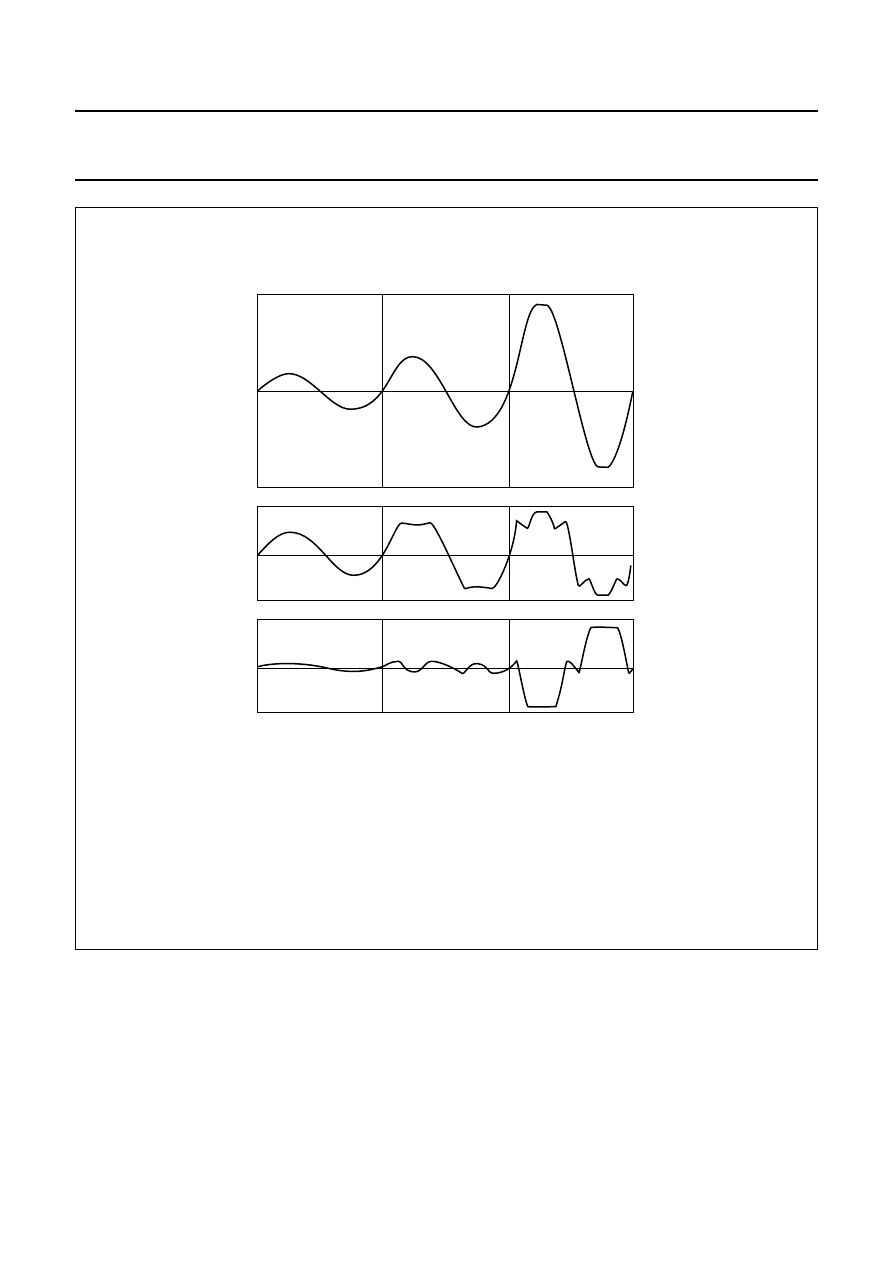
Fig.24 Output waveforms.
See Fig.7:
V
load
= V
7
−
V
8
or V
11
−
V
10
.
V
master
= V
7
or V
11
.
V
slave
= V
8
or V
10
.
handbook, full pagewidth
MBH691
0
1
2
t (ms)
3
1/2 VP
1/2 VP
0
−
VP
VP
VP
0
VP
Vload
(1)
(2)
(3)
Vmaster
Vslave
0
1998 Jul 14
20
Philips Semiconductors
Preliminary specification
2
×
25 W high efficiency car radio power
amplifier
TDA1563Q
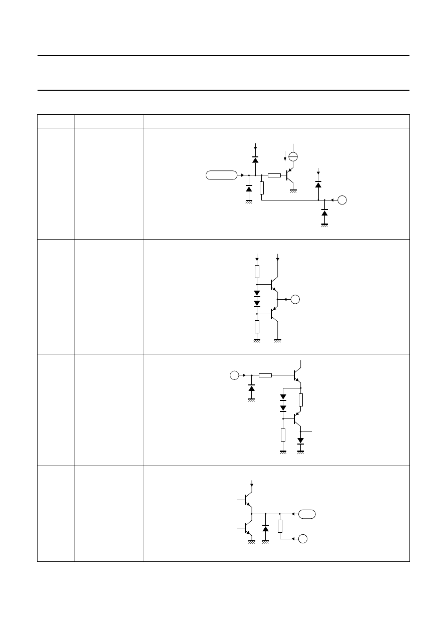
INTERNAL PIN CONFIGURATION
PIN
NAME
EQUIVALENT CIRCUIT
1, 2, 16,
17 and 3
IN1+, IN1
−
, IN2
−
,
IN2+ and CIN
4
C
SE
6
MODE
7, 11
OUT1
−
, OUT2+
MGR182
1, 2, 16, 17
3
VP1, VP2
VP1, VP2
MGR183
4
VP2
VP1
MGR184
6
MGR185
4
VP1, VP2
7, 11
1998 Jul 14
21
Philips Semiconductors
Preliminary specification
2
×
25 W high efficiency car radio power
amplifier
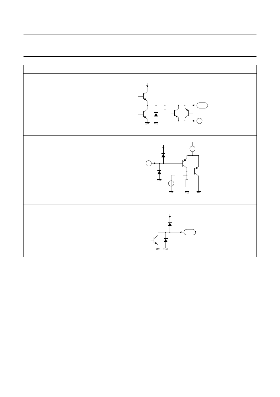
TDA1563Q
8, 10
OUT1+, OUT2
−
12
SC
14, 15
PROT, CLIP
PIN
NAME
EQUIVALENT CIRCUIT
MGR186
4
VP1, VP2
8, 10
MGR187
12
VP2
MGR188
14, 15
VP2
1998 Jul 14
22
Philips Semiconductors
Preliminary specification
2
×
25 W high efficiency car radio power
amplifier
TDA1563Q
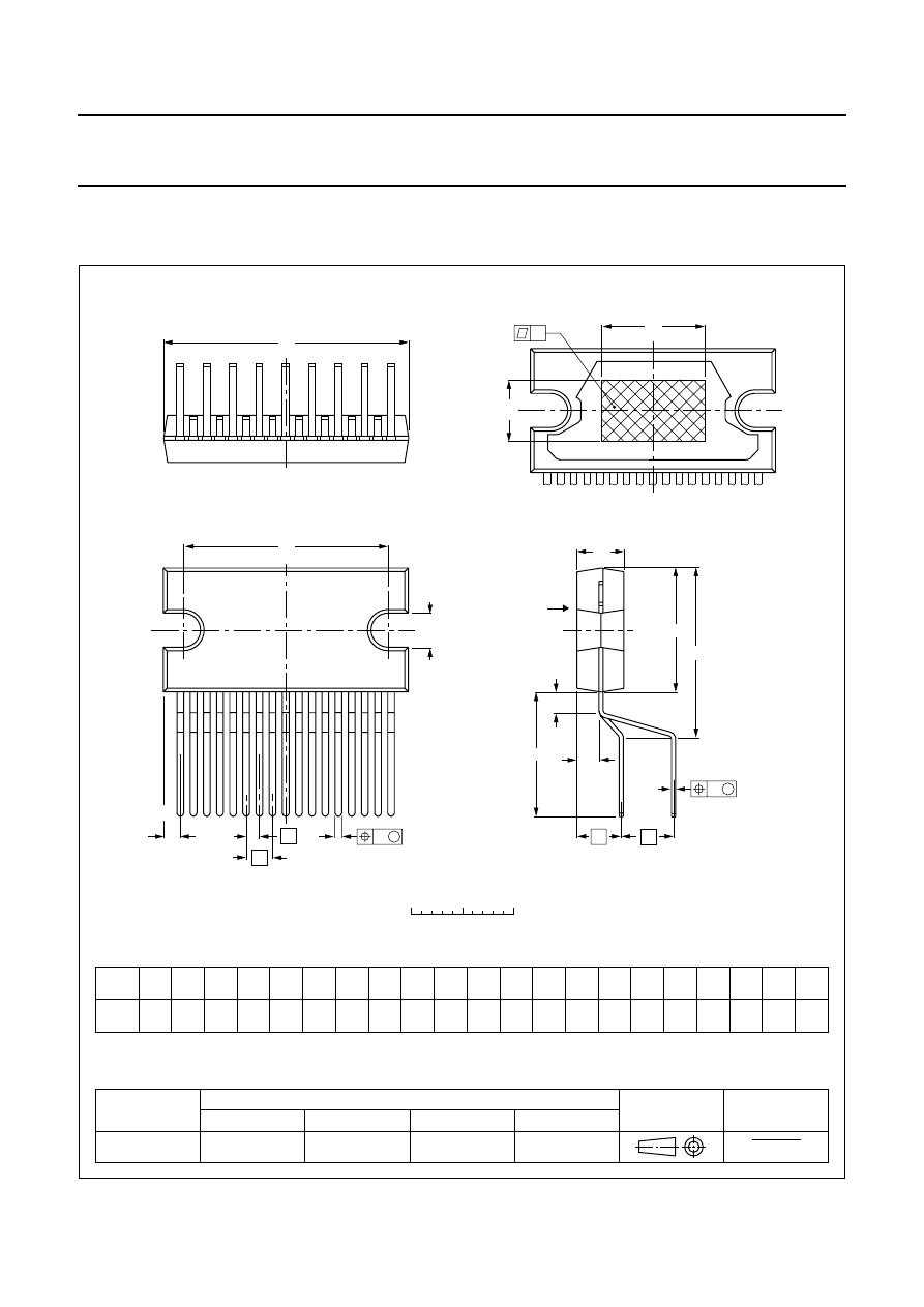
PACKAGE OUTLINE
REFERENCES
OUTLINE
VERSION
EUROPEAN
PROJECTION
ISSUE DATE
IEC
JEDEC
EIAJ
DIMENSIONS (mm are the original dimensions)
Note
1. Plastic or metal protrusions of 0.25 mm maximum per side are not included.
SOT243-1
0
5
10 mm
scale
D
L
E
A
c
A
2
L
3
Q
w
M
b
p
1
d
D
Z
e
e
x
h
1
17
j
Eh
non-concave
95-03-11
97-12-16
DBS17P: plastic DIL-bent-SIL power package; 17 leads (lead length 12 mm)
SOT243-1
view B: mounting base side
m
2
e
v
M
B
UNIT
A
e
1
A
2
b
p
c
D
(1)
E
(1)
Z
(1)
d
e
D
h
L
L
3
m
mm
17.0
15.5
4.6
4.2
0.75
0.60
0.48
0.38
24.0
23.6
20.0
19.6
10
2.54
v
0.8
12.2
11.8
1.27
e
2
5.08
2.4
1.6
E
h
6
2.00
1.45
2.1
1.8
3.4
3.1
4.3
12.4
11.0
Q
j
0.4
w
0.03
x

1998 Jul 14
23
Philips Semiconductors
Preliminary specification
2
×
25 W high efficiency car radio power
amplifier
TDA1563Q
SOLDERING
Introduction
There is no soldering method that is ideal for all IC
packages. Wave soldering is often preferred when
through-hole and surface mounted components are mixed
on one printed-circuit board. However, wave soldering is
not always suitable for surface mounted ICs, or for
printed-circuits with high population densities. In these
situations reflow soldering is often used.
This text gives a very brief insight to a complex technology.
A more in-depth account of soldering ICs can be found in
our
“Data Handbook IC26; Integrated Circuit Packages”
(order code 9398 652 90011).
Soldering by dipping or by wave
The maximum permissible temperature of the solder is
260
°
C; solder at this temperature must not be in contact
with the joint for more than 5 seconds. The total contact
time of successive solder waves must not exceed
5 seconds.
The device may be mounted up to the seating plane, but
the temperature of the plastic body must not exceed the
specified maximum storage temperature (T
stg max
). If the
printed-circuit board has been pre-heated, forced cooling
may be necessary immediately after soldering to keep the
temperature within the permissible limit.
Repairing soldered joints
Apply a low voltage soldering iron (less than 24 V) to the
lead(s) of the package, below the seating plane or not
more than 2 mm above it. If the temperature of the
soldering iron bit is less than 300
°
C it may remain in
contact for up to 10 seconds. If the bit temperature is
between 300 and 400
°
C, contact may be up to 5 seconds.
DEFINITIONS
LIFE SUPPORT APPLICATIONS
These products are not designed for use in life support appliances, devices, or systems where malfunction of these
products can reasonably be expected to result in personal injury. Philips customers using or selling these products for
use in such applications do so at their own risk and agree to fully indemnify Philips for any damages resulting from such
improper use or sale.
Data sheet status
Objective specification
This data sheet contains target or goal specifications for product development.
Preliminary specification
This data sheet contains preliminary data; supplementary data may be published later.
Product specification
This data sheet contains final product specifications.
Limiting values
Limiting values given are in accordance with the Absolute Maximum Rating System (IEC 134). Stress above one or
more of the limiting values may cause permanent damage to the device. These are stress ratings only and operation
of the device at these or at any other conditions above those given in the Characteristics sections of the specification
is not implied. Exposure to limiting values for extended periods may affect device reliability.
Application information
Where application information is given, it is advisory and does not form part of the specification.

Internet: http://www.semiconductors.philips.com
Philips Semiconductors – a worldwide company
© Philips Electronics N.V. 1998
SCA60
All rights are reserved. Reproduction in whole or in part is prohibited without the prior written consent of the copyright owner.
The information presented in this document does not form part of any quotation or contract, is believed to be accurate and reliable and may be changed
without notice. No liability will be accepted by the publisher for any consequence of its use. Publication thereof does not convey nor imply any license
under patent- or other industrial or intellectual property rights.
Middle East: see Italy
Netherlands: Postbus 90050, 5600 PB EINDHOVEN, Bldg. VB,
Tel. +31 40 27 82785, Fax. +31 40 27 88399
New Zealand: 2 Wagener Place, C.P.O. Box 1041, AUCKLAND,
Tel. +64 9 849 4160, Fax. +64 9 849 7811
Norway: Box 1, Manglerud 0612, OSLO,
Tel. +47 22 74 8000, Fax. +47 22 74 8341
Pakistan: see Singapore
Philippines: Philips Semiconductors Philippines Inc.,
106 Valero St. Salcedo Village, P.O. Box 2108 MCC, MAKATI,
Metro MANILA, Tel. +63 2 816 6380, Fax. +63 2 817 3474
Poland: Ul. Lukiska 10, PL 04-123 WARSZAWA,
Tel. +48 22 612 2831, Fax. +48 22 612 2327
Portugal: see Spain
Romania: see Italy
Russia: Philips Russia, Ul. Usatcheva 35A, 119048 MOSCOW,
Tel. +7 095 755 6918, Fax. +7 095 755 6919
Singapore: Lorong 1, Toa Payoh, SINGAPORE 319762,
Tel. +65 350 2538, Fax. +65 251 6500
Slovakia: see Austria
Slovenia: see Italy
South Africa: S.A. PHILIPS Pty Ltd., 195-215 Main Road Martindale,
2092 JOHANNESBURG, P.O. Box 7430 Johannesburg 2000,
Tel. +27 11 470 5911, Fax. +27 11 470 5494
South America: Al. Vicente Pinzon, 173, 6th floor,
04547-130 SÃO PAULO, SP, Brazil,
Tel. +55 11 821 2333, Fax. +55 11 821 2382
Spain: Balmes 22, 08007 BARCELONA,
Tel. +34 93 301 6312, Fax. +34 93 301 4107
Sweden: Kottbygatan 7, Akalla, S-16485 STOCKHOLM,
Tel. +46 8 5985 2000, Fax. +46 8 5985 2745
Switzerland: Allmendstrasse 140, CH-8027 ZÜRICH,
Tel. +41 1 488 2741 Fax. +41 1 488 3263
Taiwan: Philips Semiconductors, 6F, No. 96, Chien Kuo N. Rd., Sec. 1,
TAIPEI, Taiwan Tel. +886 2 2134 2865, Fax. +886 2 2134 2874
Thailand: PHILIPS ELECTRONICS (THAILAND) Ltd.,
209/2 Sanpavuth-Bangna Road Prakanong, BANGKOK 10260,
Tel. +66 2 745 4090, Fax. +66 2 398 0793
Turkey: Talatpasa Cad. No. 5, 80640 GÜLTEPE/ISTANBUL,
Tel. +90 212 279 2770, Fax. +90 212 282 6707
Ukraine: PHILIPS UKRAINE, 4 Patrice Lumumba str., Building B, Floor 7,
252042 KIEV, Tel. +380 44 264 2776, Fax. +380 44 268 0461
United Kingdom: Philips Semiconductors Ltd., 276 Bath Road, Hayes,
MIDDLESEX UB3 5BX, Tel. +44 181 730 5000, Fax. +44 181 754 8421
United States: 811 East Arques Avenue, SUNNYVALE, CA 94088-3409,
Tel. +1 800 234 7381
Uruguay: see South America
Vietnam: see Singapore
Yugoslavia: PHILIPS, Trg N. Pasica 5/v, 11000 BEOGRAD,
Tel. +381 11 625 344, Fax.+381 11 635 777
For all other countries apply to: Philips Semiconductors,
International Marketing & Sales Communications, Building BE-p, P.O. Box 218,
5600 MD EINDHOVEN, The Netherlands, Fax. +31 40 27 24825
Argentina: see South America
Australia: 34 Waterloo Road, NORTH RYDE, NSW 2113,
Tel. +61 2 9805 4455, Fax. +61 2 9805 4466
Austria: Computerstr. 6, A-1101 WIEN, P.O. Box 213, Tel. +43 160 1010,
Fax. +43 160 101 1210
Belarus: Hotel Minsk Business Center, Bld. 3, r. 1211, Volodarski Str. 6,
220050 MINSK, Tel. +375 172 200 733, Fax. +375 172 200 773
Belgium: see The Netherlands
Brazil: see South America
Bulgaria: Philips Bulgaria Ltd., Energoproject, 15th floor,
51 James Bourchier Blvd., 1407 SOFIA,
Tel. +359 2 689 211, Fax. +359 2 689 102
Canada: PHILIPS SEMICONDUCTORS/COMPONENTS,
Tel. +1 800 234 7381
China/Hong Kong: 501 Hong Kong Industrial Technology Centre,
72 Tat Chee Avenue, Kowloon Tong, HONG KONG,
Tel. +852 2319 7888, Fax. +852 2319 7700
Colombia: see South America
Czech Republic: see Austria
Denmark: Prags Boulevard 80, PB 1919, DK-2300 COPENHAGEN S,
Tel. +45 32 88 2636, Fax. +45 31 57 0044
Finland: Sinikalliontie 3, FIN-02630 ESPOO,
Tel. +358 9 615800, Fax. +358 9 61580920
France: 51 Rue Carnot, BP317, 92156 SURESNES Cedex,
Tel. +33 1 40 99 6161, Fax. +33 1 40 99 6427
Germany: Hammerbrookstraße 69, D-20097 HAMBURG,
Tel. +49 40 23 53 60, Fax. +49 40 23 536 300
Greece: No. 15, 25th March Street, GR 17778 TAVROS/ATHENS,
Tel. +30 1 4894 339/239, Fax. +30 1 4814 240
Hungary: see Austria
India: Philips INDIA Ltd, Band Box Building, 2nd floor,
254-D, Dr. Annie Besant Road, Worli, MUMBAI 400 025,
Tel. +91 22 493 8541, Fax. +91 22 493 0966
Indonesia: PT Philips Development Corporation, Semiconductors Division,
Gedung Philips, Jl. Buncit Raya Kav.99-100, JAKARTA 12510,
Tel. +62 21 794 0040 ext. 2501, Fax. +62 21 794 0080
Ireland: Newstead, Clonskeagh, DUBLIN 14,
Tel. +353 1 7640 000, Fax. +353 1 7640 200
Israel: RAPAC Electronics, 7 Kehilat Saloniki St, PO Box 18053,
TEL AVIV 61180, Tel. +972 3 645 0444, Fax. +972 3 649 1007
Italy: PHILIPS SEMICONDUCTORS, Piazza IV Novembre 3,
20124 MILANO, Tel. +39 2 6752 2531, Fax. +39 2 6752 2557
Japan: Philips Bldg 13-37, Kohnan 2-chome, Minato-ku,
TOKYO 108-8507, Tel. +81 3 3740 5130, Fax. +81 3 3740 5077
Korea: Philips House, 260-199 Itaewon-dong, Yongsan-ku, SEOUL,
Tel. +82 2 709 1412, Fax. +82 2 709 1415
Malaysia: No. 76 Jalan Universiti, 46200 PETALING JAYA, SELANGOR,
Tel. +60 3 750 5214, Fax. +60 3 757 4880
Mexico: 5900 Gateway East, Suite 200, EL PASO, TEXAS 79905,
Tel. +9-5 800 234 7381
Printed in The Netherlands
545102/1200/01/pp24
Date of release: 1998 Jul 14
Document order number:
9397 750 03774
Wyszukiwarka
Podobne podstrony:
TDA1564 Philips elenota pl
TDA1565TH Philips elenota pl
TDA8920 Philips elenota pl
TDA8580 Philips elenota pl
TDA1517 Philips elenota pl
TDA8942P Philips elenota pl
TDA1520 Philips elenota pl
TDA8569Q Philips elenota pl
TDA8574 Philips elenota pl
TDA8924 Philips elenota pl
TDA8922 Philips elenota pl
TDA8510J Philips elenota pl (1)
TDA8552T Philips elenota pl
TDA8567Q Philips elenota pl
TDA8943SF Philips elenota pl
TDA8576T Philips elenota pl
TDA8926 Philips elenota pl
TDA8947J Philips elenota pl
więcej podobnych podstron