
DATA SHEET
Product specification
Supersedes data of 2002 Jan 17
2004 Feb 18
INTEGRATED CIRCUITS
TDA1517; TDA1517P
2 x 6 W stereo power amplifier
2004 Feb 18
2
Philips Semiconductors
Product specification
2 x 6 W stereo power amplifier
TDA1517; TDA1517P
FEATURES
•
Requires very few external components
•
High output power
•
Fixed gain
•
Good ripple rejection
•
Mute/standby switch
•
AC and DC short-circuit safe to ground and V
P
•
Thermally protected
•
Reverse polarity safe
•
Capability to handle high energy on outputs (V
P
= 0 V)
•
No switch-on/switch-off plop
•
Electrostatic discharge protection.
GENERAL DESCRIPTION
The TDA1517 is an integrated class-B dual output
amplifier in a plastic single in-line medium power package
with fin (SIL9MPF), a plastic rectangular-bent single in-line
medium power package with fin (RBS9MPF) or a plastic
heat-dissipating dual in-line package (HDIP18). The
device is primarily developed for multi-media applications.
QUICK REFERENCE DATA
ORDERING INFORMATION
SYMBOL
PARAMETER
CONDITIONS
MIN.
TYP.
MAX.
UNIT
V
P
supply voltage
6.0
14.4
18.0
V
I
ORM
repetitive peak output current
−
−
2.5
A
I
q(tot)
total quiescent current
−
40
80
mA
I
sb
standby current
−
0.1
100
µ
A
I
sw
switch-on current
−
−
40
µ
A
|
Z
I
|
input impedance
50
−
−
k
Ω
P
o
output power
R
L
= 4
Ω
; THD = 0.5%
−
5
−
W
R
L
= 4
Ω
; THD = 10%
−
6
−
W
SVRR
supply voltage ripple rejection
f
i
= 100 Hz to 10 kHz
48
−
−
dB
α
cs
channel separation
40
−
−
dB
G
v
closed loop voltage gain
19
20
21
dB
V
no(rms)
noise output voltage (RMS value)
−
50
−
µ
V
T
c
crystal temperature
−
−
150
°
C
TYPE NUMBER
PACKAGE
NAME
DESCRIPTION
VERSION
TDA1517/N3
SIL9MPF
plastic single in-line medium power package with fin; 9 leads
SOT110-1
TDA1517/N3/S5
RBS9MPF
plastic rectangular-bent single in-line medium power package with
fin; 9 leads
SOT352-1
TDA1517P
HDIP18
plastic heat-dissipating dual in-line package; 18 leads
SOT398-1
2004 Feb 18
3
Philips Semiconductors
Product specification
2 x 6 W stereo power amplifier
TDA1517; TDA1517P
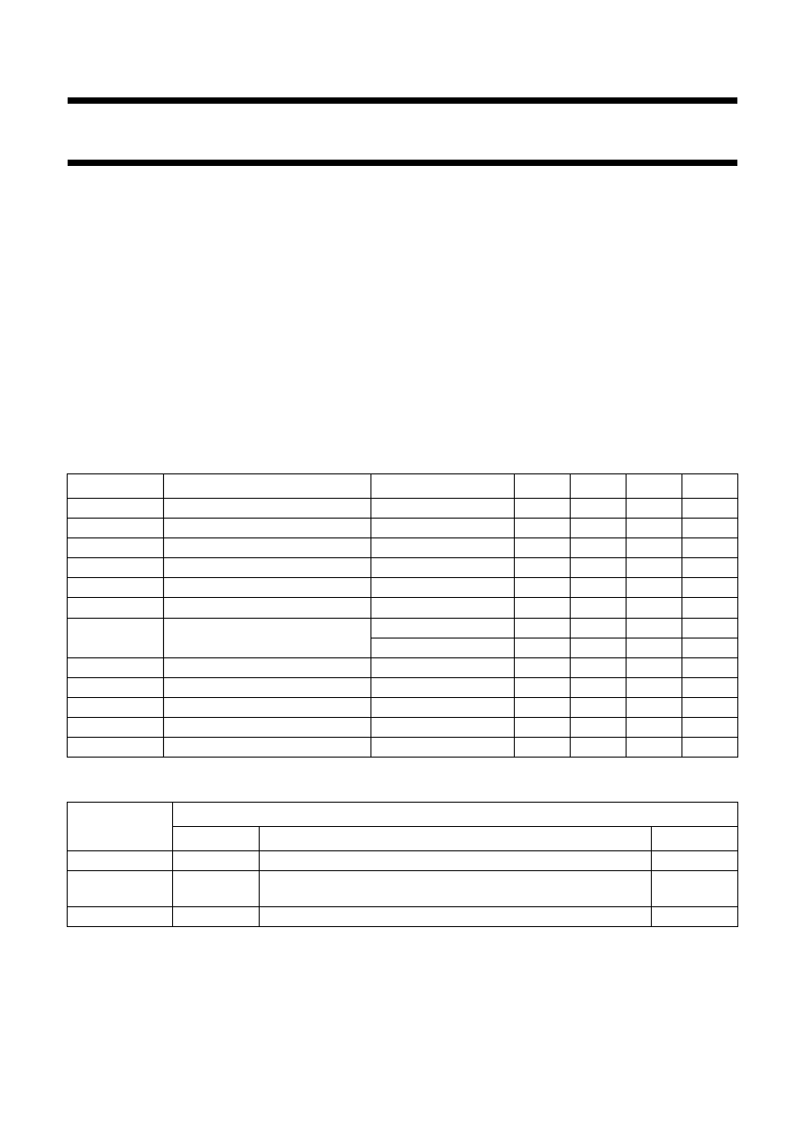
BLOCK DIAGRAM
Fig.1 Block diagram.
handbook, full pagewidth
mute/stand-by
switch input
MLC351
output 1
15 k
Ω
15 k
Ω
x 1
VA
stand-by
switch
VP
mute
switch
stand-by
reference
voltage
18 k
Ω
18 k
Ω
2
k
Ω
60
k
Ω
mute switch
Cm
power stage
4
8
mute switch
VA
VA
Cm
2
k
Ω
60
k
Ω
power stage
6
2
7
5
SGND
signal
ground
PGND
output 2
non-inverting
input 1
non-inverting
input 2
9
supply voltage
ripple rejection
output
3
1
TDA1517
mute
reference
voltage
input
reference
voltage
VP
power
ground
(substrate)
2004 Feb 18
4
Philips Semiconductors
Product specification
2 x 6 W stereo power amplifier
TDA1517; TDA1517P
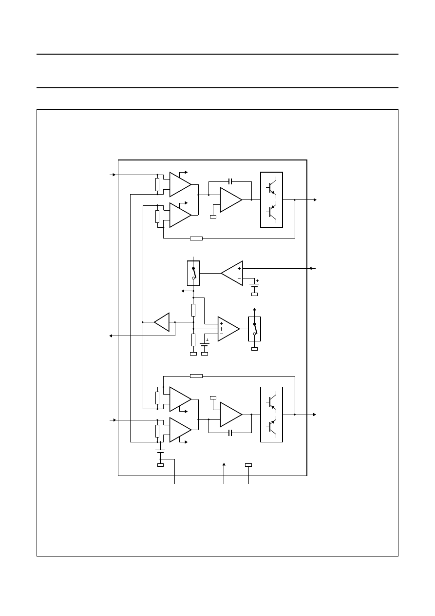
PINNING
SYMBOL
PIN
DESCRIPTION
−
INV1
1
non-inverting input 1
SGND
2
signal ground
SVRR
3
supply voltage ripple rejection output
OUT1
4
output 1
PGND
5
power ground
OUT2
6
output 2
V
P
7
supply voltage
M/SS
8
mute/standby switch input
−
INV2
9
non-inverting input 2
Fig.2
Pin configuration for SOT110-1 and
SOT352-1.
handbook, halfpage
MLC352
1
2
3
4
5
6
7
8
9
P
V
OUT2
SGND
INV1
INV2
TDA1517
OUT1
M/SS
SVRR
PGND
Fig.3 Pin configuration for SOT398-1.
Pins 10 to 18 should be connected to GND or floating.
handbook, halfpage
MLC353
1
2
3
4
5
6
7
8
9
18
17
16
15
14
13
12
11
10
P
V
OUT2
SGND
INV1
INV2
TDA1517P
OUT1
M/SS
SVRR
PGND
FUNCTIONAL DESCRIPTION
The TDA1517 contains two identical amplifiers with
differential input stages. The gain of each amplifier is fixed
at 20 dB. A special feature of the device is the
mute/standby switch which has the following features:
•
Low standby current (<100
µ
A)
•
Low mute/standby switching current
(low cost supply switch)
•
Mute condition.
2004 Feb 18
5
Philips Semiconductors
Product specification
2 x 6 W stereo power amplifier
TDA1517; TDA1517P
LIMITING VALUES
In accordance with the Absolute Maximum Rating System (IEC 60134).
THERMAL RESISTANCE
SYMBOL
PARAMETER
CONDITIONS
MIN.
MAX.
UNIT
V
P
supply voltage
operating
−
18
V
no signal
−
20
V
V
P(sc)
AC and DC short-circuit safe voltage
−
18
V
V
P(r)
reverse polarity
−
6
V
ERG
O
energy handling capability at outputs
V
P
= 0 V
−
200
mJ
I
OSM
non-repetitive peak output current
−
4
A
I
ORM
repetitive peak output current
−
2.5
A
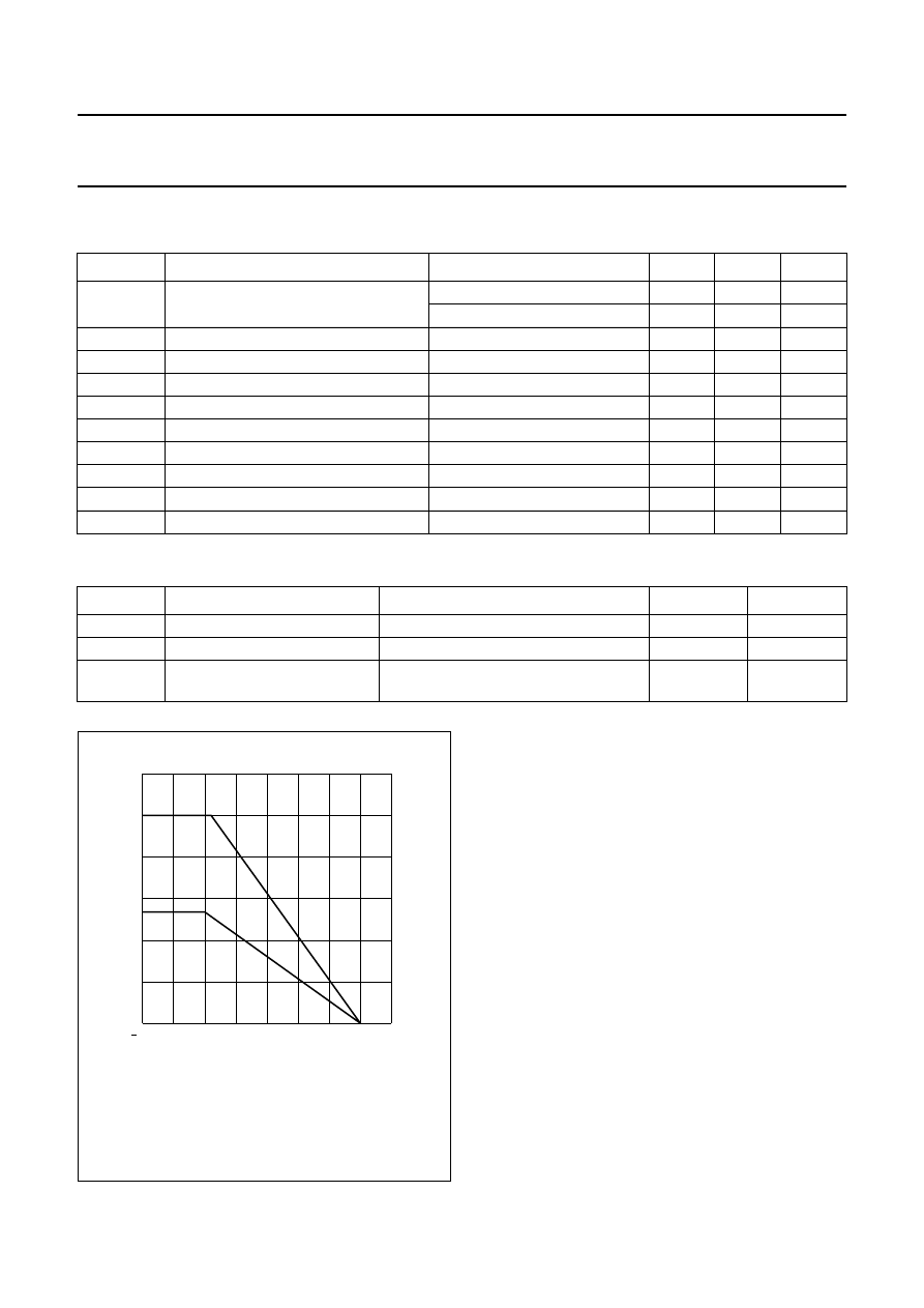
P
tot
total power dissipation
see Fig.4
−
15
W
T
stg
storage temperature
−
55
+150
°
C
T
amb
operating ambient temperature
−
40
+85
°
C
T
c
crystal temperature
−
150
°
C
SYMBOL
TYPE NUMBER
PARAMETER
VALUE
UNIT
R
th(j-c)
TDA1517/N3; TDA1517/N3/S5
thermal resistance from junction to case
8
K/W
R
th(j-p)
TDA1517P
thermal resistance from junction to pins
15
K/W
R
th(j-a)
TDA1517/N3; TDA1517/N3/S5;
TDA1517P
thermal resistance from junction to
ambient
50
K/W
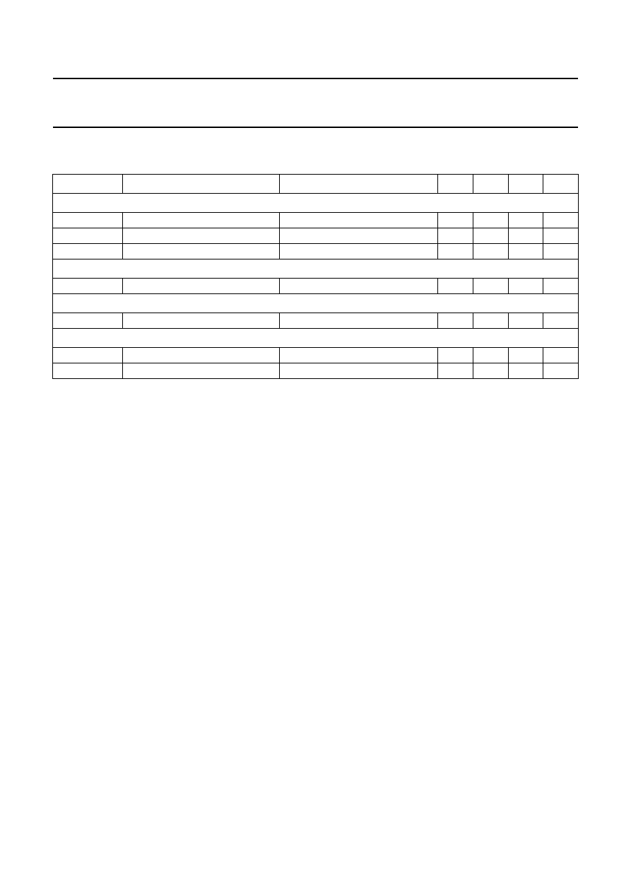
Fig.4 Power derating curve.
(1) R
th j-c
= 8 K/W.
(2) R
th j-p
= 15 K/W.
handbook, halfpage
25
0
50
150
12
0
MLC354
100
T ( C)
o
amb
P
(W)
18
6
(1)
(2)
2004 Feb 18
6
Philips Semiconductors
Product specification
2 x 6 W stereo power amplifier
TDA1517; TDA1517P
DC CHARACTERISTICS
V
P
= 14.4 V; T
amb
= 25
°
C; measured in Fig.6; unless otherwise specified.
Note
1. The circuit is DC adjusted at V
P
= 6 to 18 V and AC operating at V
P
= 8.5 to 18 V.
SYMBOL
PARAMETER
CONDITIONS
MIN.
TYP.
MAX.
UNIT
Supply
V
P
supply voltage
note 1
6.0
14.4
18.0
V
I
q(tot)
total quiescent current
−
40
80
mA
V
O
DC output voltage
−
6.95
−
V
Mute/standby switch
V
8
switch-on voltage level
see Fig.5
8.5
−
−
V
Mute condition
V
O
output signal in mute position
V
I(max)
= 1 V; f
i
= 20 Hz to 15 kHz
−
−
2
mV
Standby condition
I
sb
DC current in standby condition
−
−
100
µ
A
V
sw
switch-on current
−
12
40
µ
A

2004 Feb 18
7
Philips Semiconductors
Product specification
2 x 6 W stereo power amplifier
TDA1517; TDA1517P
AC CHARACTERISTICS
V
P
= 14.4 V; R
L
= 4
Ω
; f = 1 kHz; T
amb
= 25
°
C; measured in Fig.6; unless otherwise specified.
Notes
1. Output power is measured directly at the output pins of the IC.
2. Frequency response externally fixed.
3. Ripple rejection measured at the output with a source impedance of 0
Ω
, maximum ripple amplitude of 2 V (p-p) and
a frequency between 100 Hz and 10 kHz.
4. Noise voltage measured in a bandwidth of 20 Hz to 20 kHz.
5. Noise output voltage independent of R
s
(V
I
= 0 V).
SYMBOL
PARAMETER
CONDITIONS
MIN.
TYP.
MAX.
UNIT
P
o
output power
THD = 0.5%; note 1
4
5
−
W
THD = 10%; note 1
5.5
6.0
−
W
THD
total harmonic distortion
P
o
= 1 W
−
0.1
−
%
f
lr
low frequency roll-off
at
−
3 dB; note 2
−
45
−
Hz
f
hr
high frequency roll-off
at
−
1 dB
20
−
−
kHz
G
v
closed loop voltage gain
19
20
21
dB
SVRR
supply voltage ripple rejection
note 3
on
48
−
−
dB
mute
48
−
−
dB
standby
80
−
−
dB
|
Z
i
|
input impedance
50
60
75
k
Ω
V
no
noise output voltage
on
R
s
= 0
Ω
; note 4
−
50
−
µ
V
on
R
s
= 10
Ω
; note 4
−
70
100
µ
V
mute
note 5
−
50
−
µ
V
α
cs
channel separation
R
s
= 10
Ω
40
−
−
dB
|∆
G
v
|
channel unbalance
−
0.1
1
dB
2004 Feb 18
8
Philips Semiconductors
Product specification
2 x 6 W stereo power amplifier
TDA1517; TDA1517P
Fig.5 Standby, mute and on conditions.
handbook, halfpage
8.5
0
MLC355
V
18
6.4
3.3
2
11
(V)
,,,,,,,
,,,,,,,
,,,,,,,
,,,,,,,
,,,,,,,
,,,,,,,
,,,,,,,
,,,,,,,
ON (I = 40 mA)
P
mute (I = 40 mA)
P
standby (I 100
µ
A)
P
APPLICATION INFORMATION
Fig.6 Application circuit diagram.
handbook, full pagewidth
MLC356
100 nF
P
V
TDA1517
8
7
standby switch
220 nF
input 1
1000
µ
F
1000
µ
F
input
reference
voltage
2
5
signal
ground
power
ground
1
9
220 nF
input 2
4
6
3
2200
µ
F
internal
1/2 VP
100
µ
F
60 k
Ω
60 k
Ω
20 dB
20 dB
2004 Feb 18
9
Philips Semiconductors
Product specification
2 x 6 W stereo power amplifier
TDA1517; TDA1517P
PACKAGE OUTLINES
UNIT
A
A
max.
2
A
3
b
1
D
1
b
2
b
c
D
(1)
E
(1)
Z
max.
(1)
e
L
P
P
1
q
1
q
2
q
REFERENCES
OUTLINE
VERSION
EUROPEAN
PROJECTION
ISSUE DATE
IEC
JEDEC
JEITA
mm
18.5
17.8
3.7
8.7
8.0
A
4
15.8
15.4
1.40
1.14
0.67
0.50
1.40
1.14
0.48
0.38
21.8
21.4
21.4
20.7
6.48
6.20
3.4
3.2
2.54
1
5.9
5.7
4.4
4.2
3.9
3.4
15.1
14.9
Q
1.75
1.55
DIMENSIONS (mm are the original dimensions)
Note
1. Plastic or metal protrusions of 0.25 mm maximum per side are not included.
2.75
2.50
SOT110-1
95-02-25
03-03-12
0
5
10 mm
scale
0.25
w
D
E
A
A
c
A
2
3
A
4
q
1
q
2
L
Q
w
M
b
b
1
b
2
D
1
P
q
1
Z
e
1
9
P
seating plane
pin 1 index
SIL9MPF: plastic single in-line medium power package with fin; 9 leads
SOT110-1
2004 Feb 18
10
Philips Semiconductors
Product specification
2 x 6 W stereo power amplifier
TDA1517; TDA1517P
UNIT
A
A
max.
2
max.
A
3
b
1
D
1
b
2
b
c
D
(2)
E
(2)
Z
(2)
(1)
e
L
P
P
1
q
1
q
2
q
REFERENCES
OUTLINE
VERSION
EUROPEAN
PROJECTION
ISSUE DATE
IEC
JEDEC
JEITA
mm
14.45
13.95
8.7
8.0
3.7
1.40
1.14
0.67
0.50
1.40
1.14
0.48
0.38
21.8
21.4
21.4
20.7
6.48
6.20
3.4
3.2
2.54
1
5.9
5.7
4.4
4.2
3.8
3.3
15.1
14.9
Q
1.75
1.55
DIMENSIONS (mm are the original dimensions)
Notes
1. Dimension is specified at seating plane.
2. Plastic or metal protrusions of 0.25 mm maximum per side are not included.
2.75
2.50
SOT352-1
97-12-16
03-03-12
0
5
10 mm
scale
0.25
w
0.6
v
D
E
A
A
c
A
2
3
q
1
q
2
Q
D
1
P
q
1
P
seating plane
pin 1 index
L
w
M
v
M
b
b
1
b
2
Z
e
1
9
RBS9MPF: plastic rectangular-bent single in-line medium power package with fin; 9 leads
SOT352-1
2004 Feb 18
11
Philips Semiconductors
Product specification
2 x 6 W stereo power amplifier
TDA1517; TDA1517P
UNIT
A
max.
1
2
b
1
(1)
(1)
(1)
b
2
c
D
E
e
M
Z
H
L
REFERENCES
OUTLINE
VERSION
EUROPEAN
PROJECTION
ISSUE DATE
IEC
JEDEC
JEITA
mm
DIMENSIONS (inch dimensions are derived from the original mm dimensions)
SOT398-1
95-01-25
03-02-13
A
min.
A
max.
b
max.
w
M
E
e
1
1.40
1.14
0.67
0.50
0.47
0.38
21.85
21.35
6.5
6.2
3.9
3.1
0.25
2.54
7.62
8.32
8.02
8.7
7.7
1
4.7
0.51
3.7
inches
0.06
0.04
0.03
0.02
0.02
0.01
1.05
0.75
0.04
0.03
0.87
0.84
0.26
0.24
0.15
0.12
0.01
0.1
0.3
0.33
0.32
0.34
0.30
0.04
0.19
0.02
0.15
M
H
c
(e )
1
M
E
w
M
b
1
b
2
e
A
A
1
A
2
L
seating plane
Z
D
E
18
1
10
9
b
pin 1 index
0
5
10 mm
scale
Note
1. Plastic or metal protrusions of 0.25 mm (0.01 inch) maximum per side are not included.
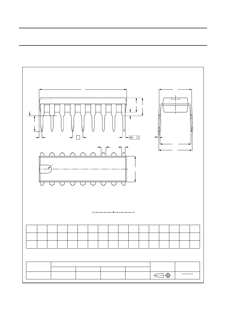
HDIP18: plastic heat-dissipating dual in-line package; 18 leads
SOT398-1

2004 Feb 18
12
Philips Semiconductors
Product specification
2 x 6 W stereo power amplifier
TDA1517; TDA1517P
SOLDERING
Introduction to soldering through-hole mount
packages
This text gives a brief insight to wave, dip and manual
soldering. A more in-depth account of soldering ICs can be
found in our
“Data Handbook IC26; Integrated Circuit
Packages” (document order number 9398 652 90011).
Wave soldering is the preferred method for mounting of
through-hole mount IC packages on a printed-circuit
board.
Soldering by dipping or by solder wave
Driven by legislation and environmental forces the
worldwide use of lead-free solder pastes is increasing.
Typical dwell time of the leads in the wave ranges from
3 to 4 seconds at 250
°
C or 265
°
C, depending on solder
material applied, SnPb or Pb-free respectively.
The total contact time of successive solder waves must not
exceed 5 seconds.
The device may be mounted up to the seating plane, but
the temperature of the plastic body must not exceed the
specified maximum storage temperature (T
stg(max)
). If the
printed-circuit board has been pre-heated, forced cooling
may be necessary immediately after soldering to keep the
temperature within the permissible limit.
Manual soldering
Apply the soldering iron (24 V or less) to the lead(s) of the
package, either below the seating plane or not more than
2 mm above it. If the temperature of the soldering iron bit
is less than 300
°
C it may remain in contact for up to
10 seconds. If the bit temperature is between
300 and 400
°
C, contact may be up to 5 seconds.
Suitability of through-hole mount IC packages for dipping and wave soldering methods
Notes
1. For SDIP packages, the longitudinal axis must be parallel to the transport direction of the printed-circuit board.
2. For PMFP packages hot bar soldering or manual soldering is suitable.
PACKAGE
SOLDERING METHOD
DIPPING
WAVE
CPGA, HCPGA
−
suitable
DBS, DIP, HDIP, RDBS, SDIP, SIL
suitable
suitable
−
not suitable

2004 Feb 18
13
Philips Semiconductors
Product specification
2 x 6 W stereo power amplifier
TDA1517; TDA1517P
DATA SHEET STATUS
Notes
1. Please consult the most recently issued data sheet before initiating or completing a design.
2. The product status of the device(s) described in this data sheet may have changed since this data sheet was
published. The latest information is available on the Internet at URL http://www.semiconductors.philips.com.
3. For data sheets describing multiple type numbers, the highest-level product status determines the data sheet status.
LEVEL
DATA SHEET
STATUS
PRODUCT
STATUS
DEFINITION
I
Objective data
Development
This data sheet contains data from the objective specification for product
development. Philips Semiconductors reserves the right to change the
specification in any manner without notice.
II
Preliminary data Qualification
This data sheet contains data from the preliminary specification.
Supplementary data will be published at a later date. Philips
Semiconductors reserves the right to change the specification without
notice, in order to improve the design and supply the best possible
product.
III
Product data
Production
This data sheet contains data from the product specification. Philips
Semiconductors reserves the right to make changes at any time in order
to improve the design, manufacturing and supply. Relevant changes will
be communicated via a Customer Product/Process Change Notification
(CPCN).
DEFINITIONS
Short-form specification
The data in a short-form
specification is extracted from a full data sheet with the
same type number and title. For detailed information see
the relevant data sheet or data handbook.
Limiting values definition
Limiting values given are in
accordance with the Absolute Maximum Rating System
(IEC 60134). Stress above one or more of the limiting
values may cause permanent damage to the device.
These are stress ratings only and operation of the device
at these or at any other conditions above those given in the
Characteristics sections of the specification is not implied.
Exposure to limiting values for extended periods may
affect device reliability.
Application information
Applications that are
described herein for any of these products are for
illustrative purposes only. Philips Semiconductors make
no representation or warranty that such applications will be
suitable for the specified use without further testing or
modification.
DISCLAIMERS
Life support applications
These products are not
designed for use in life support appliances, devices, or
systems where malfunction of these products can
reasonably be expected to result in personal injury. Philips
Semiconductors customers using or selling these products
for use in such applications do so at their own risk and
agree to fully indemnify Philips Semiconductors for any
damages resulting from such application.
Right to make changes
Philips Semiconductors
reserves the right to make changes in the products -
including circuits, standard cells, and/or software -
described or contained herein in order to improve design
and/or performance. When the product is in full production
(status ‘Production’), relevant changes will be
communicated via a Customer Product/Process Change
Notification (CPCN). Philips Semiconductors assumes no
responsibility or liability for the use of any of these
products, conveys no licence or title under any patent,
copyright, or mask work right to these products, and
makes no representations or warranties that these
products are free from patent, copyright, or mask work
right infringement, unless otherwise specified.

© Koninklijke Philips Electronics N.V. 2004
SCA76
All rights are reserved. Reproduction in whole or in part is prohibited without the prior written consent of the copyright owner.
The information presented in this document does not form part of any quotation or contract, is believed to be accurate and reliable and may be changed
without notice. No liability will be accepted by the publisher for any consequence of its use. Publication thereof does not convey nor imply any license
under patent- or other industrial or intellectual property rights.
Philips Semiconductors – a worldwide company
Contact information
For additional information please visit http://www.semiconductors.philips.com.
Fax: +31 40 27 24825
For sales offices addresses send e-mail to: sales.addresses@www.semiconductors.philips.com.
Printed in The Netherlands
R30/05/pp
14
Date of release:
2004 Feb 18
Document order number:
9397 750 12926
Document Outline
- Features
- General description
- Quick reference data
- Ordering information
- Block diagram
- Pinning
- Functional description
- Limiting values
- Thermal resistance
- DC characteristics
- AC characteristics
- Application information
- Package outlines
- Soldering
- Data sheet status
- Definitions
- Disclaimers
Wyszukiwarka
Podobne podstrony:
TDA1519C Philips elenota pl
TDA8920 Philips elenota pl
TDA8580 Philips elenota pl
TDA8942P Philips elenota pl
TDA1563Q Philips elenota pl
TDA1520 Philips elenota pl
TDA8569Q Philips elenota pl
TDA8574 Philips elenota pl
TDA8924 Philips elenota pl
TDA8922 Philips elenota pl
TDA8510J Philips elenota pl (1)
TDA8552T Philips elenota pl
TDA8567Q Philips elenota pl
TDA8943SF Philips elenota pl
TDA8576T Philips elenota pl
TDA8926 Philips elenota pl
TDA8947J Philips elenota pl
więcej podobnych podstron