
DATA SHEET
Product specification
Supersedes data of 2001 Aug 24
2004 Jan 28
INTEGRATED CIRCUITS
TDA1519C
22 W BTL or 2
×
11 W
stereo power amplifier

2004 Jan 28
2
Philips Semiconductors
Product specification
22 W BTL or 2
×
11 W
stereo power amplifier
TDA1519C
FEATURES
•
Requires very few external components for Bridge-Tied
Load (BTL) operation
•
Stereo or BTL application
•
High output power
•
Low offset voltage at output (important for BTL
applications)
•
Fixed gain
•
Good ripple rejection
•
Mute/standby switch
•
Load dump protection
•
AC and DC short-circuit safe to ground and V
P
•
Thermally protected
•
Reverse polarity safe
•
Capability to handle high energy on outputs (V
P
= 0 V)
•
No switch-on/switch-off plops
•
Protected against electrostatic discharge
•
Low thermal resistance
•
Identical inputs (inverting and non-inverting)
•
Pin compatible with TDA1519B (TDA1519C and
TDA1519CSP).
GENERAL DESCRIPTION
The TDA1519C is an integrated class-B dual output
amplifier in a 9-lead plastic single in-line power package or
20-lead heatsink small outline package.
For the TDA1519CTH (SOT418-3), the heatsink is
positioned on top of the package, which allows an external
heatsink to be mounted on top. The heatsink of the
TDA1519CTD (SOT397-1) is facing the PCB, allowing the
heatsink to be soldered onto the copper area of the PCB.
ORDERING INFORMATION
TYPE NUMBER
PACKAGE
NAME
DESCRIPTION
VERSION
TDA1519C
SIL9P
plastic single in-line power package; 9 leads
SOT131-2
TDA1519CSP
SMS9P
plastic surface mounted single in-line power package; 9 leads
SOT354-1
TDA1519CTD
HSOP20
plastic, heatsink small outline package; 20 leads
SOT397-1
TDA1519CTH
HSOP20
plastic, heatsink small outline package; 20 leads; low stand-off height
SOT418-3
2004 Jan 28
3
Philips Semiconductors
Product specification
22 W BTL or 2
×
11 W
stereo power amplifier
TDA1519C
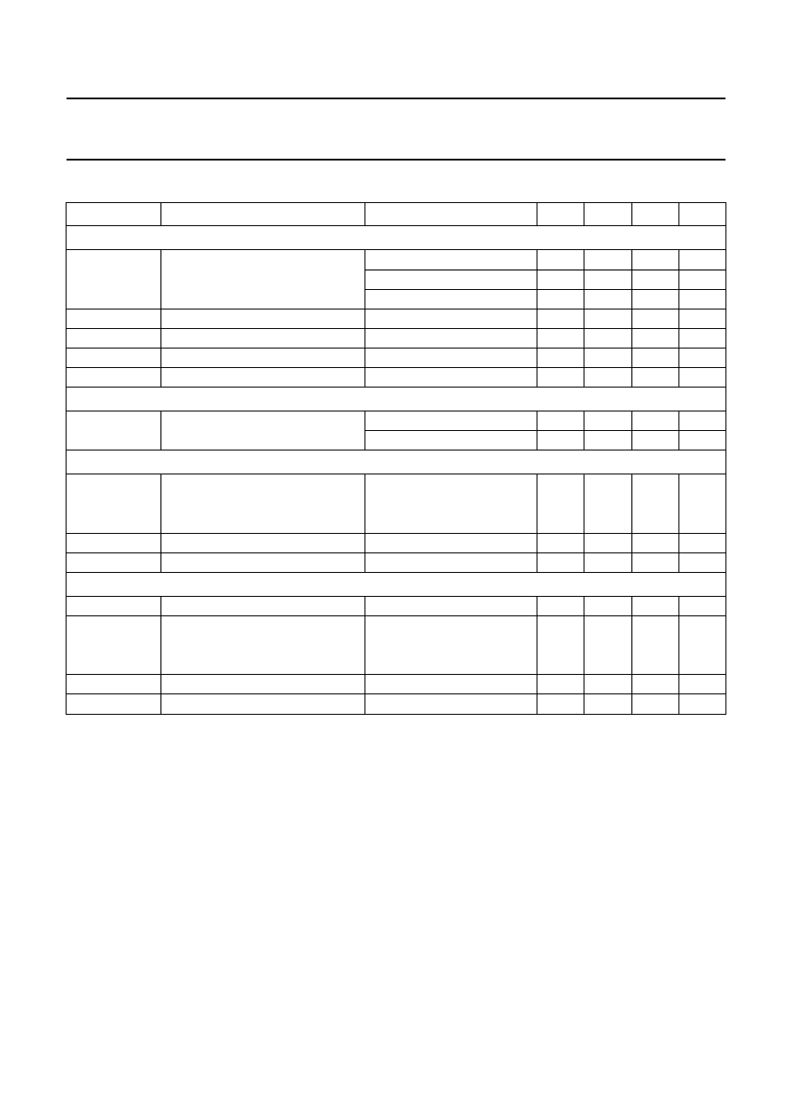
QUICK REFERENCE DATA
SYMBOL
PARAMETER
CONDITIONS
MIN.
TYP.
MAX.
UNIT
Supply
V
P
supply voltage
operating
6.0
14.4
17.5
V
non-operating
−
−
30
V
load dump protected
−
−
45
V
I
ORM
repetitive peak output current
−
−
4
A
I
q(tot)
total quiescent current
−
40
80
mA
I
stb
standby current
−
0.1
100
µ
A
I
sw(on)
switch-on current
−
−
40
µ
A
Inputs
Z
i
input impedance
BTL
25
−
−
k
Ω
stereo
50
−
−
k
Ω
Stereo application
P
o
output power
THD = 10 %
R
L
= 4
Ω
−
6
−
W
R
L
= 2
Ω
−
11
−
W
α
cs
channel separation
40
−
−
dB
V
n(o)(rms)
noise output voltage (RMS value)
−
150
−
µ
V
BTL application
P
o
output power
THD = 10 %; R
L
= 4
Ω
−
22
−
W
SVRR
supply voltage ripple rejection
R
S
= 0
Ω
f
i
= 100 Hz
34
−
−
dB
f
i
= 1 to 10 kHz
48
−
−
dB
∆
V
OO
DC output offset voltage
−
−
250
mV
T
j
junction temperature
−
−
150
°
C
2004 Jan 28
4
Philips Semiconductors
Product specification
22 W BTL or 2
×
11 W
stereo power amplifier
TDA1519C
BLOCK DIAGRAM
Fig.1 Block diagram.
MGL491
handbook, full pagewidth
60
k
Ω
input
reference
voltage
power
ground
(substrate)
+
+
−
5
signal
ground
2
7
9
6
183
Ω
18.1 k
Ω
3
TDA1519C
TDA1519CSP
15 k
Ω
15 k
Ω
VA
VA
Cm
mute switch
power stage
60
k
Ω
standby
reference
voltage
mute
reference
voltage
1
NINV
RR
INV
OUT2
M/SS
OUT1
GND1
GND2
VP
4
8
183
Ω
18.1 k
Ω
VA
Cm
mute switch
power stage
+
−
mute
switch
standby
switch
×
1
VP
The pin numbers refer to the TDA1519C and TDA1519CSP only, for TDA1519CTD and TDA1519CTH see Figs 3 and 4.
2004 Jan 28
5
Philips Semiconductors
Product specification
22 W BTL or 2
×
11 W
stereo power amplifier
TDA1519C
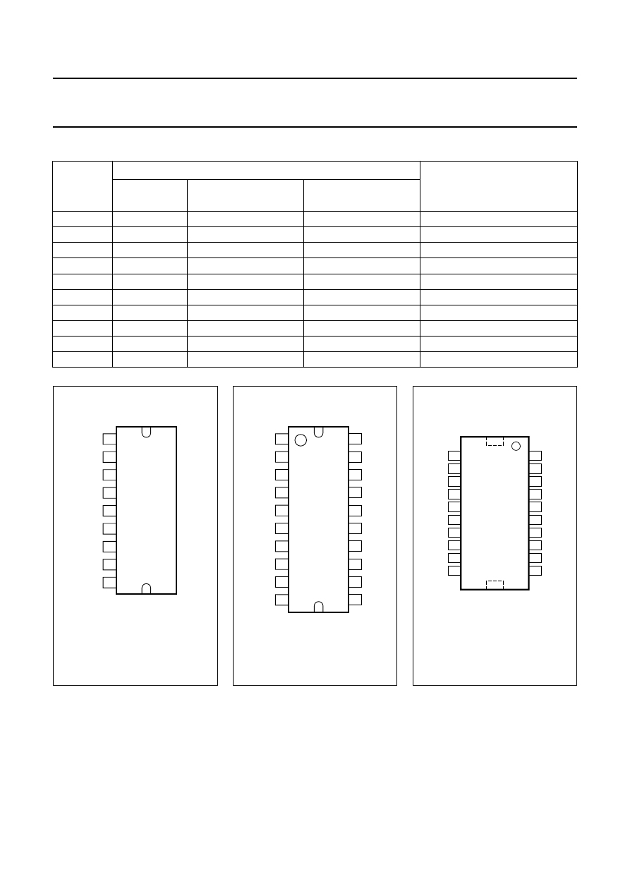
PINNING
SYMBOL
PIN
DESCRIPTION
TDA1519C;
TDA1519CSP
TDA1519CTD
TDA1519CTH
NINV
1
19
19
non-inverting input
GND1
2
20
20
ground 1 (signal)
RR
3
1
1
supply voltage ripple rejection
OUT1
4
3
3
output 1
GND2
5
5
5
ground 2 (substrate)
OUT2
6
8
8
output 2
V
P
7
10
10
positive supply voltage
M/SS
8
11
11
mute/standby switch input
INV
9
12
12
inverting input
n.c.
−
2, 4, 6, 7, 9 and 13 to 18 2, 4, 6, 7, 9 and 13 to 18 not connected
Fig.2
Pin configuration
TDA1519C and
TDA1519CSP.
halfpage
NINV
GND1
RR
OUT1
GND2
OUT2
VP
M/SS
INV
1
2
3
4
5
6
7
8
9
TDA1519C
TDA1519CSP
MGR561
fpage
RR
n.c.
OUT1
n.c.
GND2
n.c.
n.c.
OUT2
n.c.
VP
GND1
NINV
n.c.
n.c.
n.c.
n.c.
n.c.
n.c.
INV
M/SS
1
2
3
4
5
6
7
8
9
10
11
12
20
19
18
17
16
15
14
13
TDA1519CTD
MGL937
Fig.3
Pin configuration
TDA1519CTD.
TDA1519CTH
GND1
RR
NINV
n.c.
n.c.
OUT1
n.c.
n.c.
n.c.
GND2
n.c.
n.c.
n.c.
n.c.
n.c.
OUT2
INV
n.c.
M/SS
V
P
001aaa348
20
19
18
17
16
15
14
13
12
11
9
10
7
8
5
6
3
4
1
2
Fig.4
Pin configuration
TDA1519CTH.
2004 Jan 28
6
Philips Semiconductors
Product specification
22 W BTL or 2
×
11 W
stereo power amplifier
TDA1519C
FUNCTIONAL DESCRIPTION
The TDA1519C contains two identical amplifiers with
differential input stages. The gain of each amplifier is fixed
at 40 dB. A special feature of this device is the
mute/standby switch which has the following features:
•
Low standby current (<100
µ
A)
•
Low mute/standby switching current (allows for low-cost
supply switch)
•
Mute condition.
LIMITING VALUES
In accordance with the Absolute Maximum Rating System (IEC 60134).
SYMBOL
PARAMETER
CONDITIONS
MIN.
MAX.
UNIT
V
P
supply voltage
operating
−
17.5
V
non-operating
−
30
V
load dump protected;
during 50 ms; t
r
≥
2.5 ms
−
45
V
V
sc
AC and DC short-circuit-safe voltage
−
17.5
V
V
rp
reverse polarity voltage
−
6
V
E
o
energy handling capability at outputs
V
P
= 0 V
−
200
mJ
I
OSM
non-repetitive peak output current
−
6
A
I
ORM
repetitive peak output current
−
4
A
P
tot
total power dissipation
see Fig.5
−
25
W
T
j
junction temperature
−
150
°
C
T
stg
storage temperature
−
55
+150
°
C
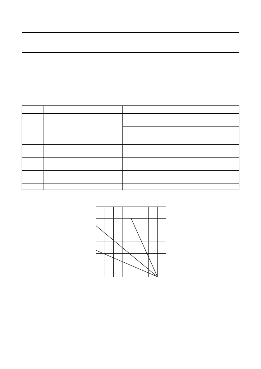
Fig.5 Power derating curve for TDA1519C.
handbook, halfpage
−
25
0
50
150
30
10
0
20
MGL492
100
Ptot
(W)
Tamb (
°
C)
(1)
(2)
(3)
(1) Infinite heatsink.
(2) R
th(c-a)
= 5 K/W.
(3) R
th(c-a)
= 13 K/W.
2004 Jan 28
7
Philips Semiconductors
Product specification
22 W BTL or 2
×
11 W
stereo power amplifier
TDA1519C
THERMAL CHARACTERISTICS
DC CHARACTERISTICS
V
P
= 14.4 V; T
amb
= 25
°
C; measured in circuit of Fig.6; unless otherwise specified.
Notes
1. The circuit is DC adjusted at V
P
= 6 to 17.5 V and AC operating at V
P
= 8.5 to 17.5 V.
2. At V
P
= 17.5 to 30 V, the DC output voltage is
≤
0.5V
P
.
SYMBOL
PARAMETER
CONDITIONS
VALUE
UNIT
R
th(j-a)
thermal resistance from junction to ambient;
TDA1519C, TDA1519CTH and TDA1519CTD
in free air
40
K/W
R
th(j-c)
thermal resistance from junction to case;
TDA1519C, TDA1519CTH and TDA1519CTD
3
K/W
SYMBOL
PARAMETER
CONDITIONS
MIN.
TYP.
MAX.
UNIT
Supply
V
P
supply voltage
note 1
6.0
14.4
17.5
V
I
q(tot)
total quiescent current
−
40
80
mA
V
O
DC output voltage
note 2
−
6.95
−
V
∆
V
OO
DC output offset voltage
−
−
250
mV
Mute/standby switch
V
sw(on)
switch-on voltage level
8.5
−
−
V
V
mute
mute voltage level
3.3
−
6.4
V
V
stb
standby voltage level
0
−
2
V
Mute/standby condition
V
o
output voltage
mute mode; V
i
= 1 V (maximum);
f
i
= 20 Hz to 15 kHz
−
−
20
mV
∆
V
OO
DC output offset voltage
mute mode
−
−
250
mV
I
stb
standby current
standby mode
−
−
100
µ
A
I
sw(on)
switch-on current
−
12
40
µ
A
2004 Jan 28
8
Philips Semiconductors
Product specification
22 W BTL or 2
×
11 W
stereo power amplifier
TDA1519C
AC CHARACTERISTICS
V
P
= 14.4 V; R
L
= 4
Ω
; f = 1 kHz; T
amb
= 25
°
C; unless otherwise specified.
SYMBOL
PARAMETER
CONDITIONS
MIN.
TYP.
MAX.
UNIT
Stereo application (see Fig.6)
P
o
output power
note 1
THD = 0.5 %
4
5
−
W
THD = 10 %
5.5
6.0
−
W
R
L
= 2
Ω
; note 1
THD = 0.5 %
7.5
8.5
−
W
THD = 10 %
10
11
−
W
THD
total harmonic distortion
P
o
= 1 W
−
0.1
−
%
f
ro(l)
low frequency roll-off
−
3 dB; note 2
−
45
−
Hz
f
ro(h)
high frequency roll-off
−
1 dB
20
−
−
kHz
G
v(cl)
closed-loop voltage gain
39
40
41
dB
SVRR
supply voltage ripple rejection
on; notes 3 and 4
40
−
−
dB
on; notes 3 and 5
45
−
−
dB
mute; notes 3 and 6
45
−
−
dB
80
−
−
dB
Z
i
input impedance
50
60
75
k
Ω
V
n(o)(rms)
noise output voltage (RMS value)
note 7
on; R
S
= 0
Ω
−
150
−
µ
V
on; R
S
= 10 k
Ω
−
250
500
µ
V
mute; note 8
−
120
−
µ
V
α
cs
channel separation
R
S
= 10 k
Ω
40
−
−
dB
∆
G
v(ub)
channel unbalance
−
0.1
1
dB
BTL application (see Fig.7)
P
o
output power
note 1
THD = 0.5 %
15
17
−
W
THD = 10 %
20
22
−
W
V
P
= 13.2 V; note 1
THD = 0.5 %
−
13
−
W
THD = 10 %
−
17.5
−
W
THD
total harmonic distortion
P
o
= 1 W
−
0.1
−
%
B
p
power bandwidth
THD = 0.5 %;
P
o
=
−
1 dB; with
respect to 15 W
−
35 to 15000
−
Hz
f
ro(l)
low frequency roll-off
−
1 dB; note 2
−
45
−
Hz
f
ro(h)
high frequency roll-off
−
1 dB
20
−
−
kHz
G
v(cl)
closed-loop voltage gain
45
46
47
dB

2004 Jan 28
9
Philips Semiconductors
Product specification
22 W BTL or 2
×
11 W
stereo power amplifier
TDA1519C
Notes
1. Output power is measured directly at the output pins of the device.
2. Frequency response externally fixed.
3. Ripple rejection measured at the output with a source impedance of 0
Ω
(maximum ripple amplitude of 2 V).
4. Frequency f = 100 Hz.
5. Frequency between 1 and 10 kHz.
6. Frequency between 100 Hz and 10 kHz.
7. Noise voltage measured in a bandwidth of 20 Hz to 20 kHz.
8. Noise output voltage independent of R
S
(V
i
= 0 V).
SVRR
supply voltage ripple rejection
34
−
−
dB
48
−
−
dB
48
−
−
dB
80
−
−
dB
Z
i
input impedance
25
30
38
k
Ω
V
n(o)(rms)
noise output voltage (RMS value)
note 7
on; R
S
= 0
Ω
−
200
−
µ
V
on; R
S
= 10 k
Ω
−
350
700
µ
V
mute; note 8
−
180
−
µ
V
SYMBOL
PARAMETER
CONDITIONS
MIN.
TYP.
MAX.
UNIT
2004 Jan 28
10
Philips Semiconductors
Product specification
22 W BTL or 2
×
11 W
stereo power amplifier
TDA1519C
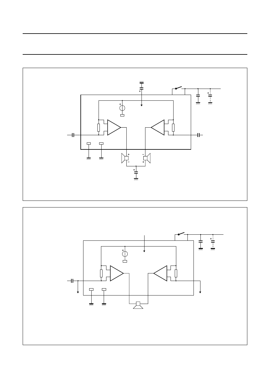
APPLICATION INFORMATION
Fig.6 Stereo application diagram (TDA1519C).
handbook, full pagewidth
2200
µ
F
1000
µ
F
100
µ
F
100
nF
220 nF
60 k
Ω
input
reference
voltage
40 dB
+
−
1
220 nF
60 k
Ω
40 dB
−
+
9
5
4
6
inverting input
non-inverting input
internal
1/2 VP
VP
power
ground
2
signal
ground
TDA1519C
3
8
7
standby switch
MGL493
Fig.7 BTL application diagram (TDA1519C).
handbook, full pagewidth
2200
µ
F
100
nF
220 nF
60 k
Ω
RL = 4
Ω
input
reference
voltage
40 dB
+
−
1
60 k
Ω
40 dB
−
+
9
5
4
6
non-inverting input
to pin 9
internal
1/2 VP
VP
power
ground
2
signal
ground
TDA1519C
3
8
7
standby switch
MGL494
to pin 1
2004 Jan 28
11
Philips Semiconductors
Product specification
22 W BTL or 2
×
11 W
stereo power amplifier
TDA1519C
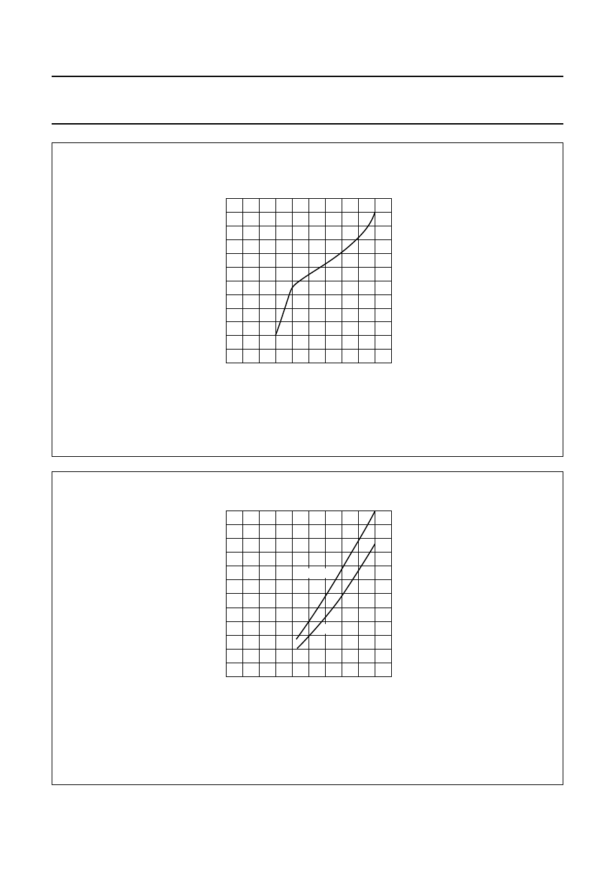
Fig.8 Total quiescent current as a function of the supply voltage.
handbook, halfpage
0
20
60
30
40
50
MGR539
4
8
12
16
Iq(tot)
(mA)
VP (V)
Fig.9 Output power as a function of the supply voltage.
handbook, halfpage
0
20
30
0
10
20
MGR540
4
8
12
16
Po
(W)
VP (V)
THD = 10%
0.5%
BTL application.
R
L
= 4
Ω
.
f
i
= 1 kHz.
2004 Jan 28
12
Philips Semiconductors
Product specification
22 W BTL or 2
×
11 W
stereo power amplifier
TDA1519C
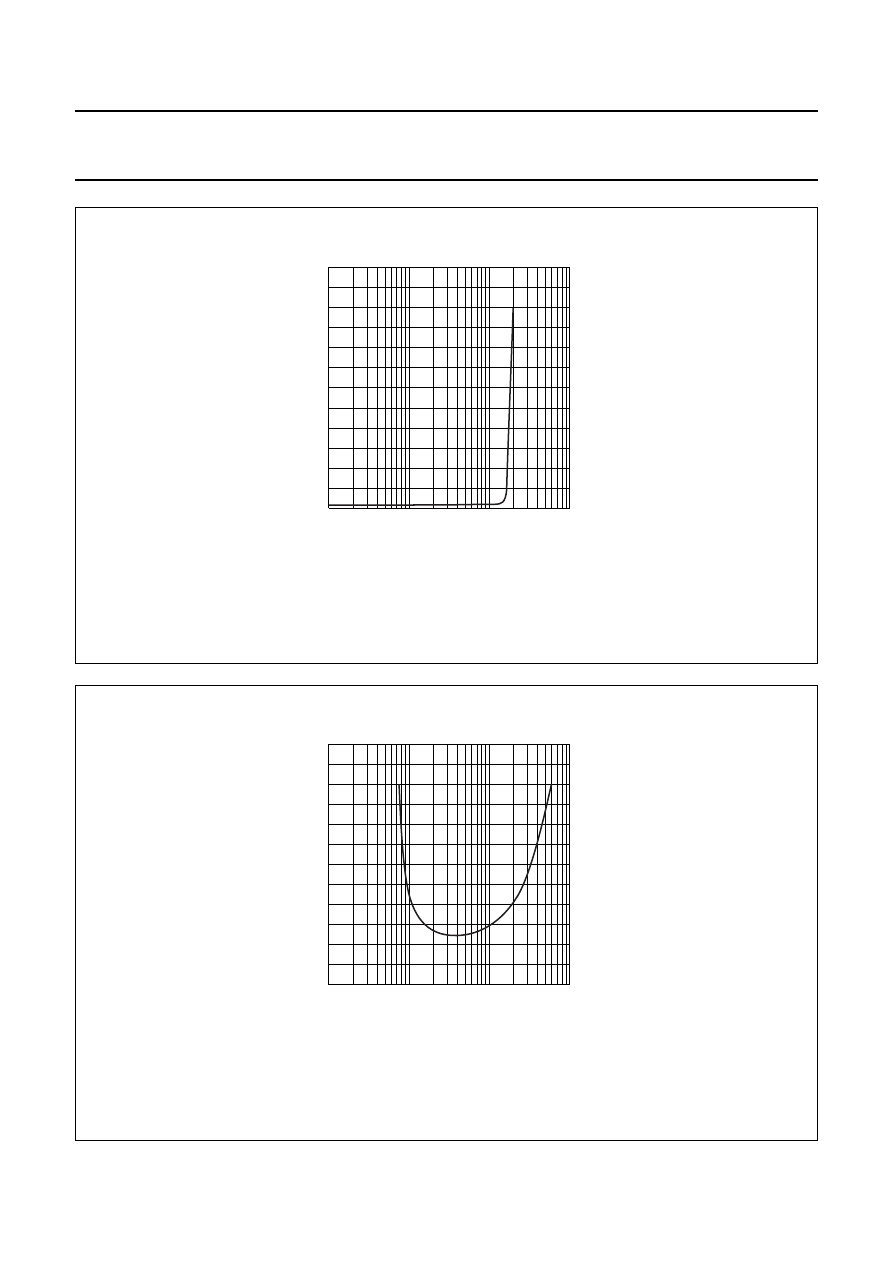
Fig.10 Total harmonic distortion as a function of the output power.
handbook, halfpage
12
0
10
−
1
1
10
10
2
MGR541
4
8
THD
(%)
Po (W)
BTL application.
R
L
= 4
Ω
.
f
i
= 1 kHz.
handbook, halfpage
0.6
0
10
10
2
10
3
10
4
MGU377
0.2
0.4
THD
(%)
fi (Hz)
Fig.11 Total harmonic distortion as a function of the operating frequency.
BTL application.
R
L
= 4
Ω
.
P
o
= 1 W.
2004 Jan 28
13
Philips Semiconductors
Product specification
22 W BTL or 2
×
11 W
stereo power amplifier
TDA1519C
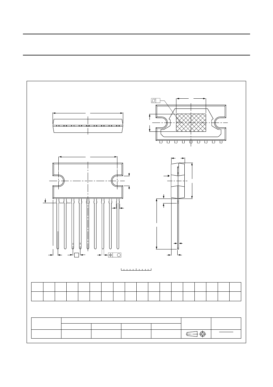
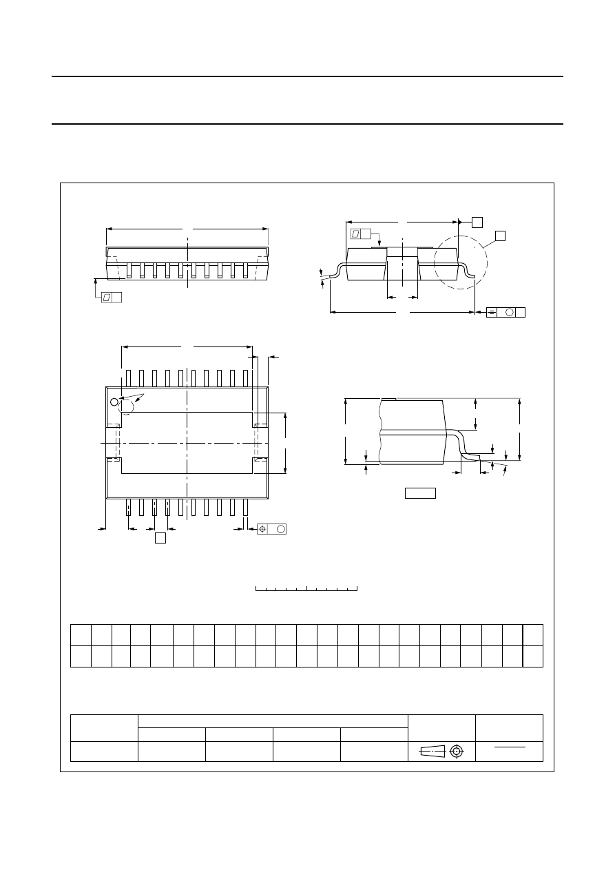
PACKAGE OUTLINES
UNIT
A
b
max.
b
p
2
c
D
(1)
E
(1)
Z
(1)
d
e
D
h
L
j
REFERENCES
OUTLINE
VERSION
EUROPEAN
PROJECTION
ISSUE DATE
IEC
JEDEC
JEITA
mm
4.6
4.4
1.1
0.75
0.60
0.48
0.38
24.0
23.6
20.0
19.6
10
2.54
12.2
11.8
3.4
3.1
A
max.
1
2
E
h
6
2.00
1.45
2.1
1.8
DIMENSIONS (mm are the original dimensions)
Note
1. Plastic or metal protrusions of 0.25 mm maximum per side are not included.
17.2
16.5
SOT131-2
99-12-17
03-03-12
0
5
10 mm
scale
Q
0.25
w
0.03
x
D
L
A
E
c
A 2
Q
w
M
b
p
d
D
Z
e
x
h
1
9
Eh
non-concave
seating plane
1
b
j
SIL9P: plastic single in-line power package; 9 leads
SOT131-2
view B: mounting base side
B
2004 Jan 28
14
Philips Semiconductors
Product specification
22 W BTL or 2
×
11 W
stereo power amplifier
TDA1519C
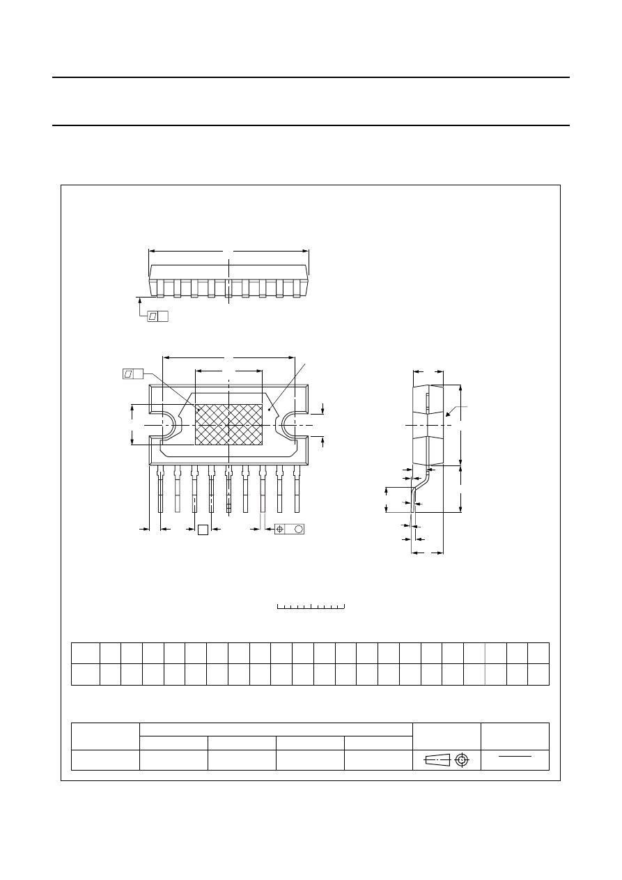
UNIT
A
A1
A2
A3
bp
c
D
(1)
E
(1)
Z
(1)
d
e
Dh
Eh
Lp
L
REFERENCES
OUTLINE
VERSION
EUROPEAN
PROJECTION
ISSUE DATE
IEC
JEDEC
JEITA
mm
4.9
4.2
0.35
0.05
4.6
4.4
0.25
0.75
0.60
24.0
23.6
0.48
0.38
10
20.0
19.6
12.2
11.8
2.54
3.4
2.8
2.1
1.9
6
3
°
0
°
2.00
1.45
3.4
3.1
DIMENSIONS (mm are the original dimensions)
Note
1. Plastic or metal protrusions of 0.25 mm maximum per side are not included.
7.4
6.6
SOT354-1
0
5
10 mm
scale
Q
j
0.15
w
x
y
θ
D
c
A1
Q
heatsink
heatsink
θ
A
Lp
(A3)
A2
0.03
0.25
w
M
b
p
d
Dh
Z
e
x
9
1
j
Eh
non-concave
99-12-17
03-03-12
SMS9P: plastic surface mounted single in-line power package; 9 leads
SOT354-1
L
E
y
2004 Jan 28
15
Philips Semiconductors
Product specification
22 W BTL or 2
×
11 W
stereo power amplifier
TDA1519C
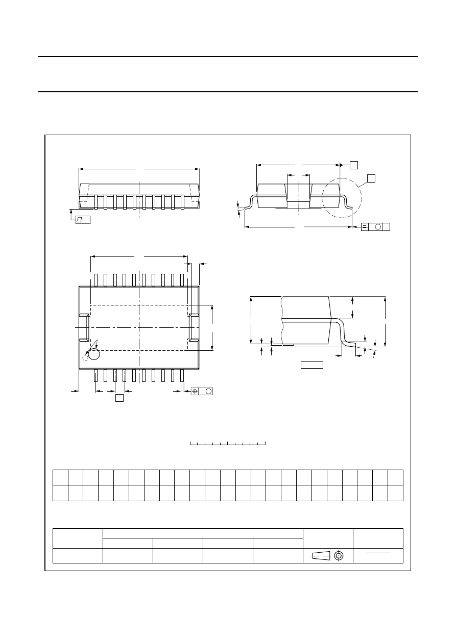
UNIT
A1
REFERENCES
OUTLINE
VERSION
EUROPEAN
PROJECTION
ISSUE DATE
03-02-18
03-07-23
IEC
JEDEC
JEITA
mm
0.3
0.1
3.6
0.35
DIMENSIONS (mm are the original dimensions)
Note
1. Plastic or metal protrusions of 0.25 mm maximum per side are not included.
SOT397-1
0
5
10 mm
scale
HSOP20: plastic, heatsink small outline package; 20 leads
SOT397-1
A
max.
D
y
HE
A1 A4
A2
bp
(A3)
E
c
v
M
A
X
A
Lp
detail X
θ
A
Q
w
M
Z
D1
D2
E2
E1
e
1
10
20
11
pin 1 index
A2
3.3
3.0
A4
0.1
0
D2
1.1
0.9
HE
14.5
13.9
Lp
1.1
0.8
Q
1.5
1.4
2.5
2.0
v
0.25
w
0.25
y
Z
8
°
0
°
θ
0.1
D1
13.0
12.6
E1
6.2
5.8
E2
2.9
2.5
bp
c
0.32
0.23
e
1.27
D
(1)
16.0
15.8
E
(1)
11.1
10.9
0.53
0.40
A3
2004 Jan 28
16
Philips Semiconductors
Product specification
22 W BTL or 2
×
11 W
stereo power amplifier
TDA1519C
UNIT
A4
(1)
REFERENCES
OUTLINE
VERSION
EUROPEAN
PROJECTION
ISSUE DATE
IEC
JEDEC
JEITA
mm
+
0.08
−
0.04
3.5
0.35
DIMENSIONS (mm are the original dimensions)
Notes
1. Limits per individual lead.
2. Plastic or metal protrusions of 0.25 mm maximum per side are not included.
SOT418-3
0
5
10 mm
scale
HSOP20: plastic, heatsink small outline package; 20 leads; low stand-off height
SOT418-3
A
max.
detail X
A2
3.5
3.2
D2
1.1
0.9
HE
14.5
13.9
Lp
1.1
0.8
Q
1.7
1.5
2.5
2.0
v
0.25
w
0.25
y
Z
8
°
0
°
θ
0.07
x
0.03
D1
13.0
12.6
E1
6.2
5.8
E2
2.9
2.5
bp
c
0.32
0.23
e
1.27
D
(2)
16.0
15.8
E
(2)
11.1
10.9
0.53
0.40
A3
A4
A2
(A3)
Lp
θ
A
Q
D
y
x
HE
E
c
v
M
A
X
A
bp
w
M
Z
D1
D2
E2
E1
e
20
11
1
10
pin 1 index
02-02-12
03-07-23

2004 Jan 28
17
Philips Semiconductors
Product specification
22 W BTL or 2
×
11 W
stereo power amplifier
TDA1519C
SOLDERING
Introduction
This text gives a very brief insight to a complex technology.
A more in-depth account of soldering ICs can be found in
our
“Data Handbook IC26; Integrated Circuit Packages”
(document order number 9398 652 90011).
There is no soldering method that is ideal for all IC
packages. Wave soldering is often preferred when
through-hole and surface mount components are mixed on
one printed-circuit board. Wave soldering can still be used
for certain surface mount ICs, but it is not suitable for fine
pitch SMDs. In these situations reflow soldering is
recommended. Driven by legislation and environmental
forces the worldwide use of lead-free solder pastes is
increasing.
Through-hole mount packages
S
OLDERING BY DIPPING OR BY SOLDER WAVE
Typical dwell time of the leads in the wave ranges from
3 to 4 seconds at 250
°
C or 265
°
C, depending on solder
material applied, SnPb or Pb-free respectively.
The total contact time of successive solder waves must not
exceed 5 seconds.
The device may be mounted up to the seating plane, but
the temperature of the plastic body must not exceed the
specified maximum storage temperature (T
stg(max)
). If the
printed-circuit board has been pre-heated, forced cooling
may be necessary immediately after soldering to keep the
temperature within the permissible limit.
M
ANUAL SOLDERING
Apply the soldering iron (24 V or less) to the lead(s) of the
package, either below the seating plane or not more than
2 mm above it. If the temperature of the soldering iron bit
is less than 300
°
C it may remain in contact for up to
10 seconds. If the bit temperature is between
300 and 400
°
C, contact may be up to 5 seconds.
Surface mount packages
R
EFLOW SOLDERING
Reflow soldering requires solder paste (a suspension of
fine solder particles, flux and binding agent) to be applied
to the printed-circuit board by screen printing, stencilling or
pressure-syringe dispensing before package placement.
Several methods exist for reflowing; for example,
convection or convection/infrared heating in a conveyor
type oven. Throughput times (preheating, soldering and
cooling) vary between 100 and 200 seconds depending
on heating method.
Typical reflow peak temperatures range from
215 to 270
°
C depending on solder paste material. The
top-surface temperature of the packages should
preferably be kept:
•
below 225
°
C (SnPb process) or below 245
°
C (Pb-free
process)
– for all the BGA, HTSSON..T and SSOP-T packages
– for packages with a thickness
≥
2.5 mm
– for packages with a thickness < 2.5 mm and a
volume
≥
350 mm
3
so called thick/large packages.
•
below 240
°
C (SnPb process) or below 260
°
C (Pb-free
process) for packages with a thickness < 2.5 mm and a
volume < 350 mm
3
so called small/thin packages.
Moisture sensitivity precautions, as indicated on packing,
must be respected at all times.
W
AVE SOLDERING
Conventional single wave soldering is not recommended
for surface mount devices (SMDs) or printed-circuit boards
with a high component density, as solder bridging and
non-wetting can present major problems.
To overcome these problems the double-wave soldering
method was specifically developed.
If wave soldering is used the following conditions must be
observed for optimal results:
•
Use a double-wave soldering method comprising a
turbulent wave with high upward pressure followed by a
smooth laminar wave.
•
For packages with leads on two sides and a pitch (e):
– larger than or equal to 1.27 mm, the footprint
longitudinal axis is preferred to be parallel to the
transport direction of the printed-circuit board;
– smaller than 1.27 mm, the footprint longitudinal axis
must be parallel to the transport direction of the
printed-circuit board.
The footprint must incorporate solder thieves at the
downstream end.
•
For packages with leads on four sides, the footprint must
be placed at a 45
°
angle to the transport direction of the
printed-circuit board. The footprint must incorporate
solder thieves downstream and at the side corners.
During placement and before soldering, the package must
be fixed with a droplet of adhesive. The adhesive can be

2004 Jan 28
18
Philips Semiconductors
Product specification
22 W BTL or 2
×
11 W
stereo power amplifier
TDA1519C
applied by screen printing, pin transfer or syringe dispensing. The package can be soldered after the adhesive is cured.
Typical dwell time of the leads in the wave ranges from 3 to 4 seconds at 250
°
C or 265
°
C, depending on solder material
applied, SnPb or Pb-free respectively.
A mildly-activated flux will eliminate the need for removal of corrosive residues in most applications.
M
ANUAL SOLDERING
Fix the component by first soldering two diagonally-opposite end leads. Use a low voltage (24 V or less) soldering iron
applied to the flat part of the lead. Contact time must be limited to 10 seconds at up to 300
°
C. When using a dedicated
tool, all other leads can be soldered in one operation within 2 to 5 seconds between 270 and 320
°
C.
Suitability of IC packages for wave, reflow and dipping soldering methods
Notes
1. For more detailed information on the BGA packages refer to the
“(LF)BGA Application Note” (AN01026); order a copy
from your Philips Semiconductors sales office.
2. All surface mount (SMD) packages are moisture sensitive. Depending upon the moisture content, the maximum
temperature (with respect to time) and body size of the package, there is a risk that internal or external package
cracks may occur due to vaporization of the moisture in them (the so called popcorn effect). For details, refer to the
Drypack information in the
“Data Handbook IC26; Integrated Circuit Packages; Section: Packing Methods”.
3. For SDIP packages, the longitudinal axis must be parallel to the transport direction of the printed-circuit board.
4. Hot bar soldering or manual soldering is suitable for PMFP packages.
5. These transparent plastic packages are extremely sensitive to reflow soldering conditions and must on no account
be processed through more than one soldering cycle or subjected to infrared reflow soldering with peak temperature
exceeding 217
°
C
±
10
°
C measured in the atmosphere of the reflow oven. The package body peak temperature
must be kept as low as possible.
6. These packages are not suitable for wave soldering. On versions with the heatsink on the bottom side, the solder
cannot penetrate between the printed-circuit board and the heatsink. On versions with the heatsink on the top side,
the solder might be deposited on the heatsink surface.
7. If wave soldering is considered, then the package must be placed at a 45
°
angle to the solder wave direction.
The package footprint must incorporate solder thieves downstream and at the side corners.
MOUNTING
PACKAGE
SOLDERING METHOD
WAVE
REFLOW
DIPPING
Through-hole mount CPGA, HCPGA
suitable
−
suitable
DBS, DIP, HDIP, RDBS, SDIP, SIL
suitable
−
−
Through-hole-
surface mount
not suitable
not suitable
−
Surface mount
SSOP-T
, TFBGA, USON, VFBGA
not suitable
suitable
−
DHVQFN, HBCC, HBGA, HLQFP, HSO,
HSOP, HSQFP, HSSON, HTQFP, HTSSOP,
HVQFN, HVSON, SMS
not suitable
suitable
−
PLCC
, SO, SOJ
suitable
suitable
−
LQFP, QFP, TQFP
not recommended
suitable
−
SSOP, TSSOP, VSO, VSSOP
not recommended
suitable
−
CWQCCN..L
not suitable
not suitable
−

2004 Jan 28
19
Philips Semiconductors
Product specification
22 W BTL or 2
×
11 W
stereo power amplifier
TDA1519C
8. Wave soldering is suitable for LQFP, QFP and TQFP packages with a pitch (e) larger than 0.8 mm; it is definitely not
suitable for packages with a pitch (e) equal to or smaller than 0.65 mm.
9. Wave soldering is suitable for SSOP, TSSOP, VSO and VSSOP packages with a pitch (e) equal to or larger than
0.65 mm; it is definitely not suitable for packages with a pitch (e) equal to or smaller than 0.5 mm.
10. Hot bar or manual soldering is suitable for PMFP packages.
11. Image sensor packages in principle should not be soldered. They are mounted in sockets or delivered pre-mounted
on flex foil. However, the image sensor package can be mounted by the client on a flex foil by using a hot bar
soldering process. The appropriate soldering profile can be provided on request.

2004 Jan 28
20
Philips Semiconductors
Product specification
22 W BTL or 2
×
11 W
stereo power amplifier
TDA1519C
DATA SHEET STATUS
Notes
1. Please consult the most recently issued data sheet before initiating or completing a design.
2. The product status of the device(s) described in this data sheet may have changed since this data sheet was
published. The latest information is available on the Internet at URL http://www.semiconductors.philips.com.
3. For data sheets describing multiple type numbers, the highest-level product status determines the data sheet status.
LEVEL
DATA SHEET
STATUS
PRODUCT
STATUS
DEFINITION
I
Objective data
Development
This data sheet contains data from the objective specification for product
development. Philips Semiconductors reserves the right to change the
specification in any manner without notice.
II
Preliminary data Qualification
This data sheet contains data from the preliminary specification.
Supplementary data will be published at a later date. Philips
Semiconductors reserves the right to change the specification without
notice, in order to improve the design and supply the best possible
product.
III
Product data
Production
This data sheet contains data from the product specification. Philips
Semiconductors reserves the right to make changes at any time in order
to improve the design, manufacturing and supply. Relevant changes will
be communicated via a Customer Product/Process Change Notification
(CPCN).
DEFINITIONS
Short-form specification
The data in a short-form
specification is extracted from a full data sheet with the
same type number and title. For detailed information see
the relevant data sheet or data handbook.
Limiting values definition
Limiting values given are in
accordance with the Absolute Maximum Rating System
(IEC 60134). Stress above one or more of the limiting
values may cause permanent damage to the device.
These are stress ratings only and operation of the device
at these or at any other conditions above those given in the
Characteristics sections of the specification is not implied.
Exposure to limiting values for extended periods may
affect device reliability.
Application information
Applications that are
described herein for any of these products are for
illustrative purposes only. Philips Semiconductors make
no representation or warranty that such applications will be
suitable for the specified use without further testing or
modification.
DISCLAIMERS
Life support applications
These products are not
designed for use in life support appliances, devices, or
systems where malfunction of these products can
reasonably be expected to result in personal injury. Philips
Semiconductors customers using or selling these products
for use in such applications do so at their own risk and
agree to fully indemnify Philips Semiconductors for any
damages resulting from such application.
Right to make changes
Philips Semiconductors
reserves the right to make changes in the products -
including circuits, standard cells, and/or software -
described or contained herein in order to improve design
and/or performance. When the product is in full production
(status ‘Production’), relevant changes will be
communicated via a Customer Product/Process Change
Notification (CPCN). Philips Semiconductors assumes no
responsibility or liability for the use of any of these
products, conveys no licence or title under any patent,
copyright, or mask work right to these products, and
makes no representations or warranties that these
products are free from patent, copyright, or mask work
right infringement, unless otherwise specified.

© Koninklijke Philips Electronics N.V. 2004
SCA76
All rights are reserved. Reproduction in whole or in part is prohibited without the prior written consent of the copyright owner.
The information presented in this document does not form part of any quotation or contract, is believed to be accurate and reliable and may be changed
without notice. No liability will be accepted by the publisher for any consequence of its use. Publication thereof does not convey nor imply any license
under patent- or other industrial or intellectual property rights.
Philips Semiconductors – a worldwide company
Contact information
For additional information please visit http://www.semiconductors.philips.com.
Fax: +31 40 27 24825
For sales offices addresses send e-mail to: sales.addresses@www.semiconductors.philips.com.
Printed in The Netherlands
R32/04/pp
21
Date of release:
2004 Jan 28
Document order number:
9397 750 12599
Document Outline
- Features
- General description
- Ordering information
- Quick reference data
- Block diagram
- Pinning
- Functional description
- Limiting values
- Thermal characteristics
- DCcharacteristics
- ACcharacteristics
- Application information
- Package outlines
- Soldering
- Data sheet status
- Definitions
- Disclaimers
Wyszukiwarka
Podobne podstrony:
TDA1517 Philips elenota pl
TDA8920 Philips elenota pl
TDA8580 Philips elenota pl
TDA8942P Philips elenota pl
TDA1563Q Philips elenota pl
TDA1520 Philips elenota pl
TDA8569Q Philips elenota pl
TDA8574 Philips elenota pl
TDA8924 Philips elenota pl
TDA8922 Philips elenota pl
TDA8510J Philips elenota pl (1)
TDA8552T Philips elenota pl
TDA8567Q Philips elenota pl
TDA8943SF Philips elenota pl
TDA8576T Philips elenota pl
TDA8926 Philips elenota pl
TDA8947J Philips elenota pl
więcej podobnych podstron