
DATA SHEET
Product specification
Supersedes data of 1997 Feb 20
File under Integrated Circuits, IC01
2001 Feb 21
INTEGRATED CIRCUITS
TDA8563AQ
2
×
40 W/2
Ω
stereo BTL car radio
power amplifier with diagnostic
facility

2001 Feb 21
2
Philips Semiconductors
Product specification
2
×
40 W/2
Ω
stereo BTL car radio power
amplifier with diagnostic facility
TDA8563AQ
FEATURES
•
Requires very few external components
•
High output power
•
4
Ω
and 2
Ω
load impedance
•
Low output offset voltage
•
Fixed gain
•
Diagnostic facility (distortion, short-circuit and
temperature detection)
•
Good ripple rejection
•
Mode select switch (operating, mute and standby)
•
Load dump protection
•
Short-circuit safe to ground, to V
P
and across the load
•
Low power dissipation in any short-circuit condition
•
Thermally protected
•
Reverse polarity safe
•
Electrostatic discharge protection
•
No switch-on/switch-off plop
•
Flexible leads
•
Low thermal resistance.
GENERAL DESCRIPTION
The TDA8563AQ is an integrated class-B output amplifier
in a 13-lead single-in-line (SIL) power package. It contains
2
×
40 W/2
Ω
amplifiers in a BTL configuration.
The device is primarily developed for car radio
applications.
QUICK REFERENCE DATA
ORDERING INFORMATION
SYMBOL
PARAMETER
CONDITIONS
MIN.
TYP.
MAX.
UNIT
V
P
operating supply voltage
6.0
14.4
18
V
I
ORM
repetitive peak output current
−
−
7.5
A
I
q(tot)
total quiescent current
−
115
−
mA
I
stb
standby current
−
0.1
10
µ
A
I
sw
switch-on current
−
−
40
µ
A
Z
I
input impedance
25
30
−
k
Ω
P
o
output power
R
L
= 4
Ω
; THD = 10%
−
25
−
W
R
L
= 2
Ω
; THD = 10%
−
40
−
W
SVRR
supply voltage ripple rejection
R
s
= 0
Ω
−
60
−
dB
α
cs
channel separation
R
s
= 10 k
Ω
−
50
−
dB
G
v
closed loop voltage gain
25
26
27
dB
V
n(o)
noise output voltage
R
s
= 0
Ω
−
−
120
µ
V
TYPE NUMBER
PACKAGE
NAME
DESCRIPTION
VERSION
TDA8563AQ
DBS13P
plastic DIL-bent-SIL power package; 13 leads (lead length 12 mm)
SOT141-6
2001 Feb 21
3
Philips Semiconductors
Product specification
2
×
40 W/2
Ω
stereo BTL car radio power
amplifier with diagnostic facility
TDA8563AQ
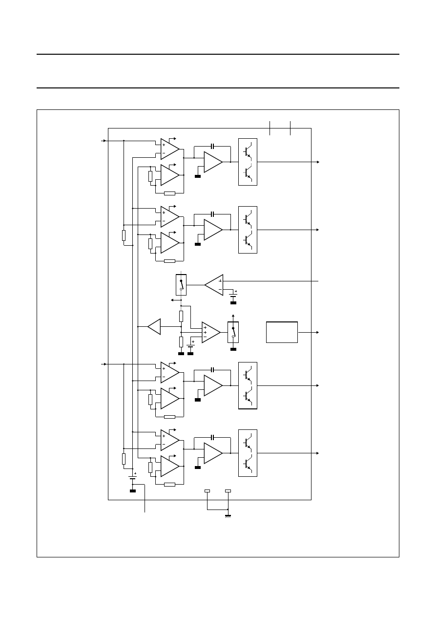
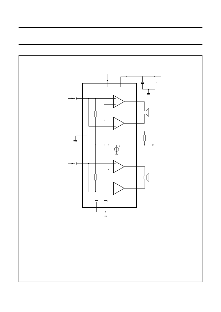
BLOCK DIAGRAM
Fig.1 Block diagram.
handbook, full pagewidth
mode switch
MGL073
output 1A
15 k
Ω
15 k
Ω
x1
VA
stand-by
switch
VP
mute
switch
stand-by
reference
voltage
PROTECTIONS
Load dump
Soar
Thermal
Short - circuit
Reverse polarity
3
10
VP1
VP2
20.7 k
Ω
2.3
k
Ω
20.7 k
Ω
2.3
k
Ω
20.7 k
Ω
2.3
k
Ω
20.7 k
Ω
2.3
k
Ω
mute switch
VA
Cm
power stage
mute switch
VA
Cm
power stage
30
k
Ω
4
6
11
mute switch
VA
Cm
power stage
mute switch
VA
Cm
power stage
30
k
Ω
9
7
2
5
8
ground (signal)
GND1
GND2
power ground (substrate)
output 2B
output 2A
output 1B
input 1
input 2
13
1
TDA8563AQ
mute
reference
voltage
input
reference
voltage
12
diagnostic
output
DIAGNOSTIC
INTERFACE
2001 Feb 21
4
Philips Semiconductors
Product specification
2
×
40 W/2
Ω
stereo BTL car radio power
amplifier with diagnostic facility
TDA8563AQ
PINNING
FUNCTIONAL DESCRIPTION
The TDA8563AQ contains two identical amplifiers and can
be used for bridge applications. The gain of each amplifier
is fixed at 26 dB. Special features of the device are as
follows.
Mode select switch (pin 11)
•
Standby: low supply current
•
Mute: input signal suppressed
•
Operating: normal on condition.
Since this pin has a very low input current (
<
40
µ
A), a low
cost supply switch can be applied.
To avoid switch-on plops, it is advised to keep the amplifier
in the mute mode during
≥
100 ms (charging of the input
capacitors at pin 1 and pin 13). During switching from
standby to mute, the slope should be at least 18 V/s.
This can be achieved by:
•
Microprocessor control
•
External timing circuit (see Fig.7).
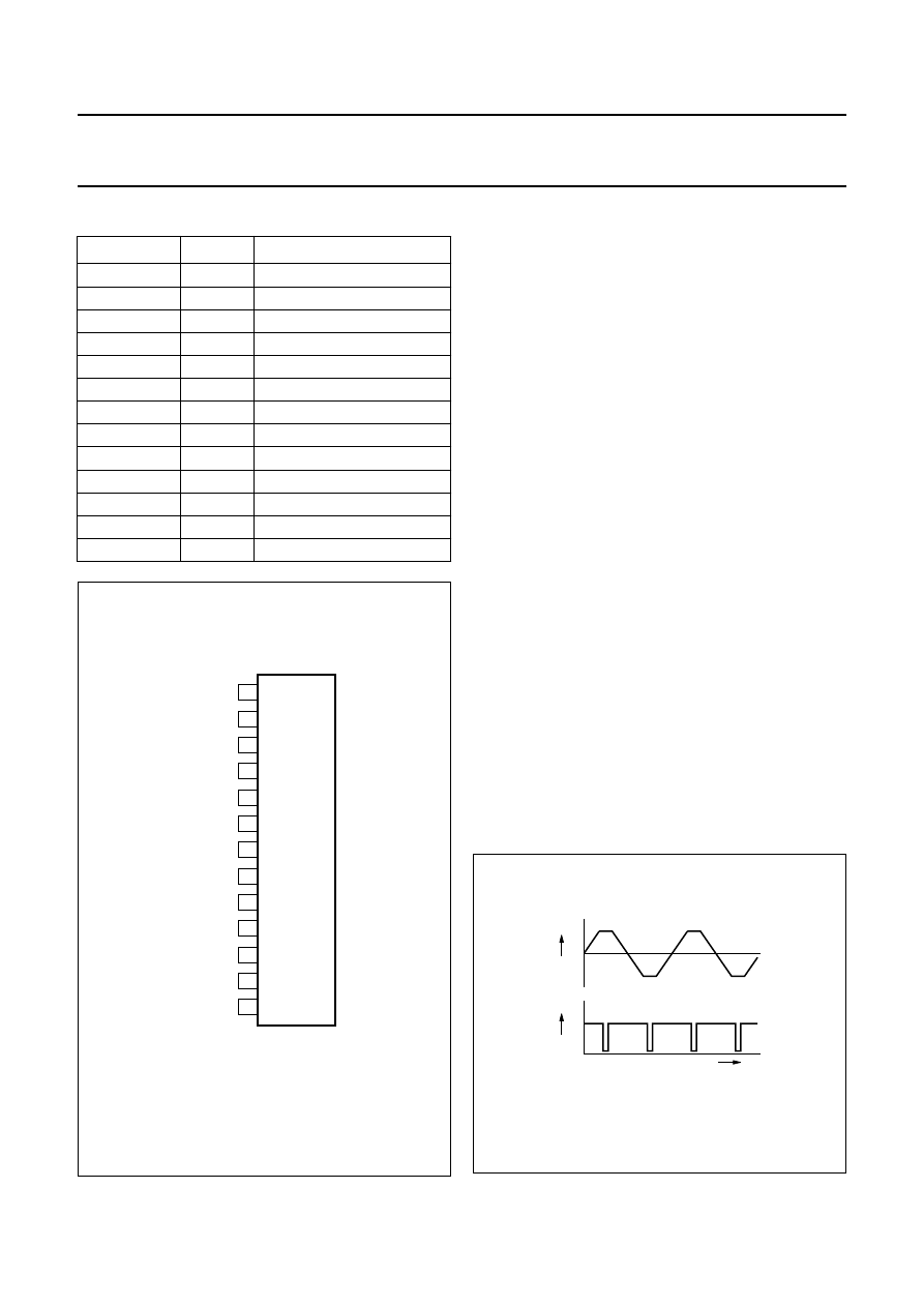
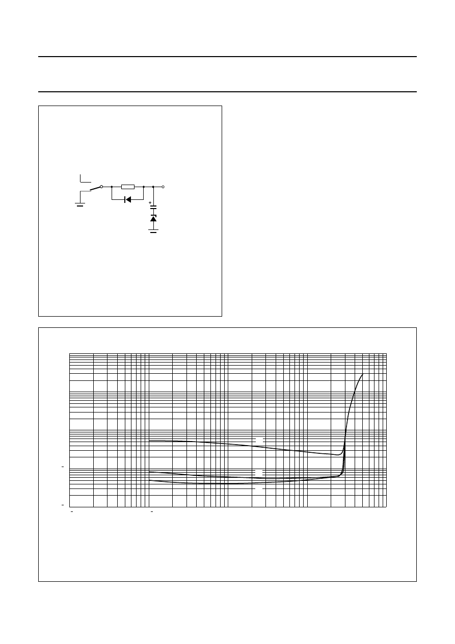
Diagnostic output (pin 12)
D
YNAMIC DISTORTION DETECTOR
(DDD)
At the onset of clipping of one or more output stages, the
dynamic distortion detector becomes active and pin 12
goes LOW. This information can be used to drive a sound
processor or DC volume control to attenuate the input
signal and thus limit the distortion. The output level of
pin 12 is independent of the number of channels that are
clipping (see Fig.3).
SYMBOL
PIN
DESCRIPTION
IN 1
1
input 1
GND(S)
2
signal ground
V
P1
3
supply voltage 1
OUT 1A
4
output 1A
GND1
5
power ground 1
OUT 1B
6
output 1B
OUT 2A
7
output 2A
GND2
8
power ground 2
OUT 2B
9
output 2B
V
P2
10
supply voltage 2
MODE
11
mode switch input
V
DIAG
12
diagnostic output
IN 2
13
input 2
Fig.2 Pin configuration.
handbook, halfpage
1
2
3
4
5
6
7
8
9
10
11
12
13
MGL075
TDA8563AQ
IN 1
GND(S)
V P1
OUT 1A
GND1
OUT 1B
OUT 2A
GND2
OUT 2B
VP2
MODE
IN 2
DIAG
V
Fig.3 Distortion detector waveform.
handbook, halfpage
V
0
VP
VO
0
t
MGA721
12
2001 Feb 21
5
Philips Semiconductors
Product specification
2
×
40 W/2
Ω
stereo BTL car radio power
amplifier with diagnostic facility
TDA8563AQ
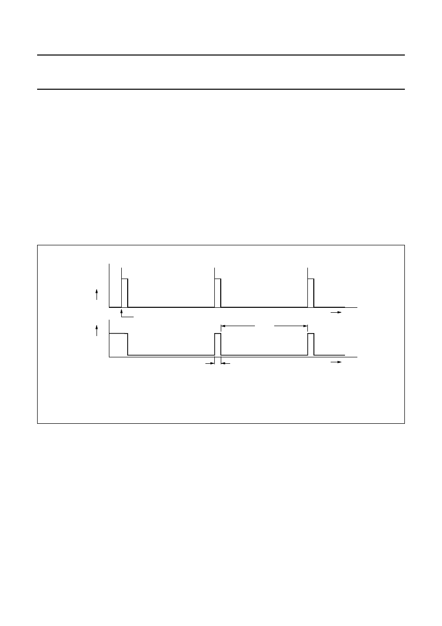
S
HORT
-
CIRCUIT PROTECTION
When a short-circuit occurs at one or more outputs to
ground or to the supply voltage, the output stages are
switched off until the short-circuit is removed and the
device is switched on again, with a delay of approximately
20 ms, after removal of the short-circuit. During this
short-circuit condition, pin 12 is continuously LOW.
When a short-circuit across the load of one or both
channels occurs the output stages are switched off during
approximately 20 ms. After that time it is checked during
approximately 50
µ
s to see whether the short-circuit is still
present. Due to this duty cycle of 50
µ
s/20 ms the average
current consumption during this short-circuit condition is
very low (approximately 40 mA).
During this short-circuit condition, pin 12 is LOW for 20 ms
and HIGH for 50
µ
s (see Fig.4).
The power dissipation in any short-circuit condition is very
low.
T
EMPERATURE DETECTION
When the virtual junction temperature T
vj
reaches 150
°
C,
pin 12 will become continuously low.
O
PEN COLLECTOR OUTPUT
Pin 12 is an open collector output, which allows pin 12 of
more devices being tied together.
Fig.4 Short-circuit waveform.
handbook, full pagewidth
MGA722
short-circuit over the load
20 ms
µ
50 s
t
t
VP
current
in
output
stage
V12
2001 Feb 21
6
Philips Semiconductors
Product specification
2
×
40 W/2
Ω
stereo BTL car radio power
amplifier with diagnostic facility
TDA8563AQ
LIMITING VALUES
In accordance with the Absolute Maximum Rating System (IEC 60134).
THERMAL CHARACTERISTICS
SYMBOL
PARAMETER
CONDITIONS
MIN.
MAX.
UNIT
V
P
supply voltage
operating
−
18
V
non-operating
−
30
V
load dump protection
during 50 ms; t
r
≥
2.5 ms
−
45
V
V
psc
AC and DC short-circuit safe voltage
−
18
V
V
rp
reverse polarity
−
6
V
I
OSM
non-repetitive peak output current
−
10
A
I
ORM
repetitive peak output current
−
7.5
A
P
tot
total power dissipation
−
60
W
T
stg
storage temperature
−
55
+150
°
C
T
amb
ambient temperature
−
40
+85
°
C
T
vj
virtual junction temperature
−
150
°
C
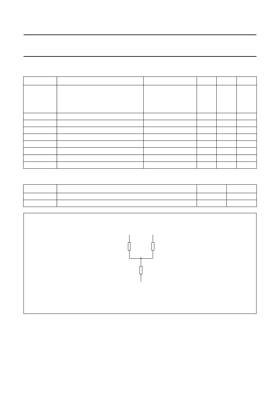
SYMBOL
PARAMETER
VALUE
UNIT
R
th(j-a)
thermal resistance from junction to ambient in free air
40
K/W
R
th(j-c)
thermal resistance from junction to case (see Fig.5)
1.3
K/W
Fig.5 Equivalent thermal resistance network.
handbook, halfpage
2.2 K/W
0.2 K/W
2.2 K/W
virtual junction
output 1
output 2
case
MBA624

2001 Feb 21
7
Philips Semiconductors
Product specification
2
×
40 W/2
Ω
stereo BTL car radio power
amplifier with diagnostic facility
TDA8563AQ
DC CHARACTERISTICS
V
P
= 14.4 V; T
amb
= 25
°
C; measured in Fig.6; unless otherwise specified.
Notes
1. The circuit is DC adjusted at V
P
= 6 to 18 V and AC operating at V
P
= 8.5 to 18 V.
2. At 18 V
<
V
P
<
30 V the DC output voltage
≤
1
⁄
2
V
P
.
SYMBOL
PARAMETER
CONDITIONS
MIN.
TYP.
MAX.
UNIT
Supply
V
P
supply voltage
note 1
6.0
14.4
18
V
I
q
quiescent current
R
L
=
∞
−
115
180
mA
Operating condition
V
11
mode switch voltage level
8.5
−
V
P
V
I
11
mode switch current
V
11
= 14.4 V
−
15
40
µ
A
V
O
DC output voltage
note 2
−
7.0
−
V
V
OO
DC output offset voltage
−
−
100
mV
Mute condition
V
11
mode switch voltage level
3.3
−
6.4
V
V
O
DC output voltage
note 2
−
7.0
−
V
V
OO
DC output offset voltage
−
−
60
mV
∆
V
OO
DELTA DC output offset voltage
mute/operating
−
−
60
mV
Standby condition
V
11
mode switch voltage level
0
−
2
V
I
stb
standby current
−
0.1
10
µ
A
Diagnostic output
V
12
diagnostic output voltage
any short-circuit or clipping
−
−
0.6
V

2001 Feb 21
8
Philips Semiconductors
Product specification
2
×
40 W/2
Ω
stereo BTL car radio power
amplifier with diagnostic facility
TDA8563AQ
AC CHARACTERISTICS
V
P
= 14.4 V; R
L
= 2
Ω
; f = 1 kHz; T
amb
= 25
°
C; measured in Fig.6; unless otherwise specified.
Notes
1. Dynamic distortion detector active.
2. Frequency response externally fixed.
3. V
ripple
= V
ripple(max)
= 2 V (p-p); R
s
= 0
Ω
.
4. B = 20 Hz to 20 kHz; R
s
= 0
Ω
.
5. B = 20 Hz to 20 kHz; R
s
= 10 k
Ω
.
6. B = 20 Hz to 20 kHz; independent of R
s
.
7. P
o
= 25 W; R
s
= 10 k
Ω
.
8. V
i
= V
i(max)
= 1 V (RMS).
SYMBOL
PARAMETER
CONDITIONS
MIN.
TYP.
MAX.
UNIT
P
o
output power
THD = 0.5%
25
30
−
W
THD = 10%
33
40
−
W
THD = 30%
45
55
−
W
THD = 0.5%; V
P
= 13.2 V
−
25
−
W
THD = 10%; V
P
= 13.2 V
−
35
−
W
THD
total harmonic distortion
P
o
= 1 W
−
0.1
−
%
V
12
≤
0.6 V; note 1
−
2.2
−
%
B
power bandwidth
THD = 0.5%; P
o
=
−
1 dB
with respect to 25 W
−
20 to 20000
−
Hz
f
ro(l)
low frequency roll-off
at
−
1 dB; note 2
−
25
−
Hz
f
ro(h)
high frequency roll-off
at
−
1 dB
20
−
−
kHz
G
v
closed loop voltage gain
25
26
27
dB
SVRR
supply voltage ripple rejection
on
note 3
50
−
−
dB
mute
note 3
50
−
−
dB
standby
note 3
80
−
−
dB
Z
i
input impedance
25
30
38
k
Ω
V
n(o)
noise output voltage
on
note 4
−
85
120
µ
V
on
note 5
−
100
−
µ
V
mute
note 6
−
60
−
µ
V
α
cs
channel separation
note 7
45
−
−
dB
∆
G
v
channel unbalance
−
−
1
dB
V
o(mute)
output voltage in mute
note 8
−
−
2
mV

2001 Feb 21
9
Philips Semiconductors
Product specification
2
×
40 W/2
Ω
stereo BTL car radio power
amplifier with diagnostic facility
TDA8563AQ
AC CHARACTERISTICS
V
P
= 14.4 V; R
L
= 4
Ω
; f = 1 kHz; T
amb
= 25
°
C; measured in Fig.6; unless otherwise specified.
SYMBOL
PARAMETER
CONDITIONS
MIN.
TYP.
MAX.
UNIT
P
o
output power
THD = 0.5%
16
19
−
W
THD = 10%
21
25
−
W
THD = 30%
28
35
−
W
THD = 0.5%; V
P
= 13.2 V
−
15
−
W
THD = 10%; V
P
= 13.2 V
−
21
−
W
THD
total harmonic distortion
P
o
= 1 W
−
0.1
−
%
2001 Feb 21
10
Philips Semiconductors
Product specification
2
×
40 W/2
Ω
stereo BTL car radio power
amplifier with diagnostic facility
TDA8563AQ
TEST AND APPLICATION INFORMATION
Fig.6 Stereo BTL test/application diagram.
handbook, full pagewidth
MGL074
100
nF
mode switch
11
3
10
470 nF
1
4
6
470 nF
13
9
7
5
8
VP
TDA8563AQ
2200
µ
F
30
k
Ω
reference
voltage
2
ground (signal)
30
k
Ω
input 2
input 1
power ground (substrate)
12
10 k
Ω
VP
diagnostic
output
(1) To avoid high energy switching pulses which can feedback to the inputs it is advisable to ensure that the value of the resistor at pin 12 is
≥
10 k
Ω
.
2001 Feb 21
11
Philips Semiconductors
Product specification
2
×
40 W/2
Ω
stereo BTL car radio power
amplifier with diagnostic facility
TDA8563AQ
Diagnostic output
Special care must be taken in the printed-circuit board
layout to separate pin 12 from pin 1 and pin 13, to
minimize the crosstalk between the diagnostic output and
the inputs.
Mode select switch
To avoid switch-on plops, it is advised to keep the amplifier
in the mute mode during
>
100 ms (charging of the input
capacitors at pin 1 and pin 13).
The circuit in Fig.7 slowly ramps up the voltage at the
mode select switch pin when switching on and results in
fast muting when switching off.
Fig.7 Mode select switch circuitry.
handbook, halfpage
+
VP
MODE
MGD959
BZX79C/3.9V
10 k
Ω
47
µ
F
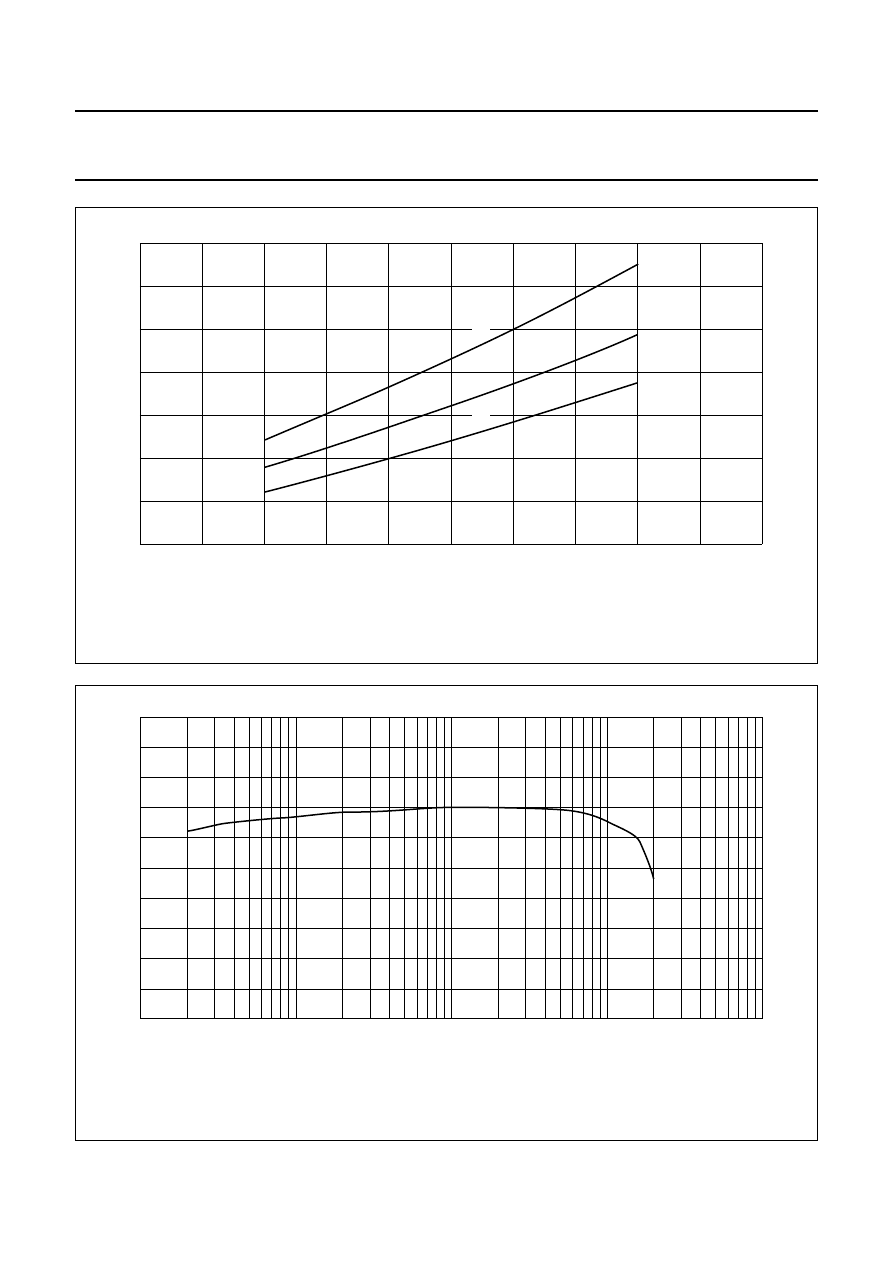
Fig.8 Total harmonic distortion as a function of output power; V
P
= 14.4 V; R
L
= 2
Ω
.
handbook, full pagewidth
10
2
MLB667
10
1
10
1
10
2
10
1
10
P (W)
o
10
2
1
10
2
THD
(%)
(1)
(2)
(3)
(1) f = 10 kHz.
(2) f = 1 Hz.
(3) f = 100 Hz.
2001 Feb 21
12
Philips Semiconductors
Product specification
2
×
40 W/2
Ω
stereo BTL car radio power
amplifier with diagnostic facility
TDA8563AQ
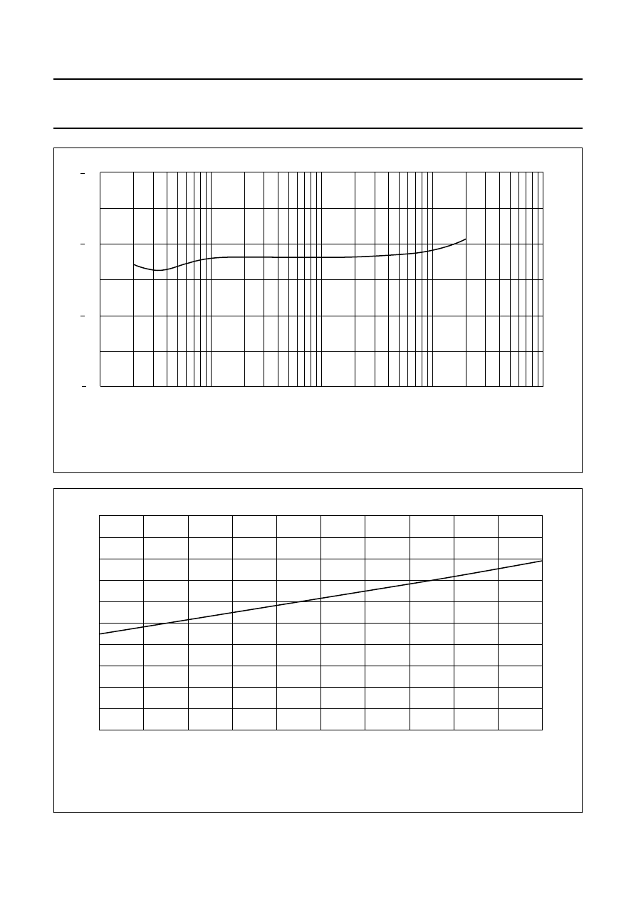
Fig.9 Output power as a function of supply voltage; f = 1 kHz; R
L
= 2
Ω
.
(1) THD = 30%.
(2) THD = 10%.
(3) THD = 0.5%.
handbook, full pagewidth
18
70
0
8
10
12
14
16
MGA905
10
20
30
40
Po
(W)
V (V)
P
(3)
(2)
50
60
(1)
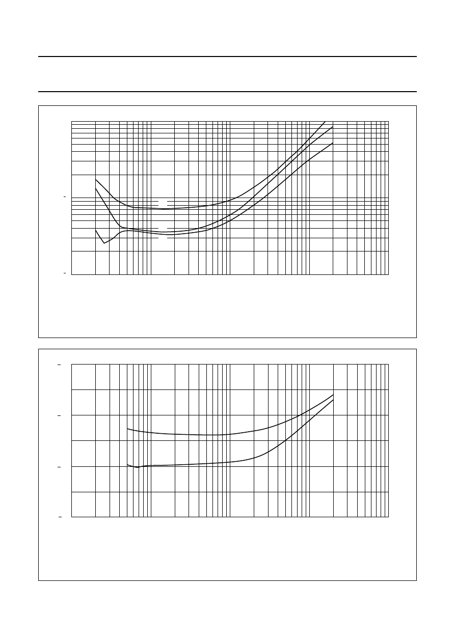
Fig.10 Output power as a function of frequency; THD = 0.5%; V
P
= 14.4 V; R
L
= 2
Ω
.
handbook, full pagewidth
23
10
5
MLB668
10
4
10
3
10
2
10
25
27
29
31
f (Hz)
Po
(W)
33
2001 Feb 21
13
Philips Semiconductors
Product specification
2
×
40 W/2
Ω
stereo BTL car radio power
amplifier with diagnostic facility
TDA8563AQ
Fig.11 Total harmonic distortion as a function of frequency; V
P
= 14.4 V; R
L
= 2
Ω
.
handbook, full pagewidth
10
5
MLB669
10
4
10
3
10
2
10
1
10
2
f (Hz)
10
1
THD
(%)
(2)
(3)
(1)
(1) P
o
= 0.1 W.
(2) P
o
= 1 W.
(3) P
o
= 10 W.
Fig.12 Ripple rejection as a function of frequency; V
P
= 14.4 V; V
ripple
= 2 V (p-p); R
s
= 0
Ω
.
handbook, full pagewidth
80
10
5
MLB670
10
4
10
3
10
2
10
70
60
50
f (Hz)
SVRR
(dB)
(1)
(2)
(1) On condition.
(2) Mute condition.
2001 Feb 21
14
Philips Semiconductors
Product specification
2
×
40 W/2
Ω
stereo BTL car radio power
amplifier with diagnostic facility
TDA8563AQ
Fig.13 Channel separation as a function of frequency; V
P
= 14.4 V; P
o
= 25 W; R
L
= 2
Ω
; R
s
= 10 k
Ω
.
handbook, full pagewidth
70
10
5
MLB671
10
4
10
3
10
2
10
60
50
40
f (Hz)
(dB)
α
cs
Fig.14 Quiescent current as a function of supply voltage; R
L
=
∞
.
handbook, full pagewidth
18
150
50
8
10
12
14
16
MGA909
70
90
110
130
V (V)
P
Iq
(mA)
2001 Feb 21
15
Philips Semiconductors
Product specification
2
×
40 W/2
Ω
stereo BTL car radio power
amplifier with diagnostic facility
TDA8563AQ
PACKAGE OUTLINE
UNIT
A
e
1
A
2
b
p
c
D
(1)
E
(1)
Z
(1)
d
e
D
h
L
L
3
m
REFERENCES
OUTLINE
VERSION
EUROPEAN
PROJECTION
ISSUE DATE
IEC
JEDEC
EIAJ
mm
17.0
15.5
4.6
4.4
0.75
0.60
0.48
0.38
24.0
23.6
20.0
19.6
10
3.4
v
0.8
12.2
11.8
1.7
e
2
5.08
2.4
1.6
E
h
6
2.00
1.45
2.1
1.8
3.4
3.1
4.3
DIMENSIONS (mm are the original dimensions)
Note
1. Plastic or metal protrusions of 0.25 mm maximum per side are not included.
12.4
11.0
SOT141-6
0
5
10 mm
scale
Q
j
0.25
w
0.03
x
D
L
E
A
c
A
2
m
L
3
Q
w
M
b
p
1
d
D
Z
e
2
e
e
x
h
1
13
j
Eh
non-concave
view B: mounting base side
97-12-16
99-12-17
DBS13P: plastic DIL-bent-SIL power package; 13 leads (lead length 12 mm)
SOT141-6
v
M
B

2001 Feb 21
16
Philips Semiconductors
Product specification
2
×
40 W/2
Ω
stereo BTL car radio power
amplifier with diagnostic facility
TDA8563AQ
SOLDERING
Introduction to soldering through-hole mount
packages
This text gives a brief insight to wave, dip and manual
soldering. A more in-depth account of soldering ICs can be
found in our
“Data Handbook IC26; Integrated Circuit
Packages” (document order number 9398 652 90011).
Wave soldering is the preferred method for mounting of
through-hole mount IC packages on a printed-circuit
board.
Soldering by dipping or by solder wave
The maximum permissible temperature of the solder is
260
°
C; solder at this temperature must not be in contact
with the joints for more than 5 seconds.
The total contact time of successive solder waves must not
exceed 5 seconds.
The device may be mounted up to the seating plane, but
the temperature of the plastic body must not exceed the
specified maximum storage temperature (T
stg(max)
). If the
printed-circuit board has been pre-heated, forced cooling
may be necessary immediately after soldering to keep the
temperature within the permissible limit.
Manual soldering
Apply the soldering iron (24 V or less) to the lead(s) of the
package, either below the seating plane or not more than
2 mm above it. If the temperature of the soldering iron bit
is less than 300
°
C it may remain in contact for up to
10 seconds. If the bit temperature is between
300 and 400
°
C, contact may be up to 5 seconds.
Suitability of through-hole mount IC packages for dipping and wave soldering methods
Note
1. For SDIP packages, the longitudinal axis must be parallel to the transport direction of the printed-circuit board.
PACKAGE
SOLDERING METHOD
DIPPING
WAVE
DBS, DIP, HDIP, SDIP, SIL
suitable
suitable
(1)

2001 Feb 21
17
Philips Semiconductors
Product specification
2
×
40 W/2
Ω
stereo BTL car radio power
amplifier with diagnostic facility
TDA8563AQ
DATA SHEET STATUS
Note
1. Please consult the most recently issued data sheet before initiating or completing a design.
DATA SHEET STATUS
PRODUCT
STATUS
DEFINITIONS
(1)
Objective specification
Development
This data sheet contains the design target or goal specifications for
product development. Specification may change in any manner without
notice.
Preliminary specification
Qualification
This data sheet contains preliminary data, and supplementary data will be
published at a later date. Philips Semiconductors reserves the right to
make changes at any time without notice in order to improve design and
supply the best possible product.
Product specification
Production
This data sheet contains final specifications. Philips Semiconductors
reserves the right to make changes at any time without notice in order to
improve design and supply the best possible product.
DEFINITIONS
Short-form specification
The data in a short-form
specification is extracted from a full data sheet with the
same type number and title. For detailed information see
the relevant data sheet or data handbook.
Limiting values definition
Limiting values given are in
accordance with the Absolute Maximum Rating System
(IEC 60134). Stress above one or more of the limiting
values may cause permanent damage to the device.
These are stress ratings only and operation of the device
at these or at any other conditions above those given in the
Characteristics sections of the specification is not implied.
Exposure to limiting values for extended periods may
affect device reliability.
Application information
Applications that are
described herein for any of these products are for
illustrative purposes only. Philips Semiconductors make
no representation or warranty that such applications will be
suitable for the specified use without further testing or
modification.
DISCLAIMERS
Life support applications
These products are not
designed for use in life support appliances, devices, or
systems where malfunction of these products can
reasonably be expected to result in personal injury. Philips
Semiconductors customers using or selling these products
for use in such applications do so at their own risk and
agree to fully indemnify Philips Semiconductors for any
damages resulting from such application.
Right to make changes
Philips Semiconductors
reserves the right to make changes, without notice, in the
products, including circuits, standard cells, and/or
software, described or contained herein in order to
improve design and/or performance. Philips
Semiconductors assumes no responsibility or liability for
the use of any of these products, conveys no licence or title
under any patent, copyright, or mask work right to these
products, and makes no representations or warranties that
these products are free from patent, copyright, or mask
work right infringement, unless otherwise specified.

2001 Feb 21
18
Philips Semiconductors
Product specification
2
×
40 W/2
Ω
stereo BTL car radio power
amplifier with diagnostic facility
TDA8563AQ
NOTES

2001 Feb 21
19
Philips Semiconductors
Product specification
2
×
40 W/2
Ω
stereo BTL car radio power
amplifier with diagnostic facility
TDA8563AQ
NOTES

© Philips Electronics N.V.
SCA
All rights are reserved. Reproduction in whole or in part is prohibited without the prior written consent of the copyright owner.
The information presented in this document does not form part of any quotation or contract, is believed to be accurate and reliable and may be changed
without notice. No liability will be accepted by the publisher for any consequence of its use. Publication thereof does not convey nor imply any license
under patent- or other industrial or intellectual property rights.
Internet: http://www.semiconductors.philips.com
2001
71
Philips Semiconductors – a worldwide company
For all other countries apply to: Philips Semiconductors,
Marketing Communications, Building BE-p, P.O. Box 218, 5600 MD EINDHOVEN,
The Netherlands, Fax. +31 40 27 24825
Argentina: see South America
Australia: 3 Figtree Drive, HOMEBUSH, NSW 2140,
Tel. +61 2 9704 8141, Fax. +61 2 9704 8139
Austria: Computerstr. 6, A-1101 WIEN, P.O. Box 213,
Tel. +43 1 60 101 1248, Fax. +43 1 60 101 1210
Belarus: Hotel Minsk Business Center, Bld. 3, r. 1211, Volodarski Str. 6,
220050 MINSK, Tel. +375 172 20 0733, Fax. +375 172 20 0773
Belgium: see The Netherlands
Brazil: see South America
Bulgaria: Philips Bulgaria Ltd., Energoproject, 15th floor,
51 James Bourchier Blvd., 1407 SOFIA,
Tel. +359 2 68 9211, Fax. +359 2 68 9102
Canada: PHILIPS SEMICONDUCTORS/COMPONENTS,
Tel. +1 800 234 7381, Fax. +1 800 943 0087
China/Hong Kong: 501 Hong Kong Industrial Technology Centre,
72 Tat Chee Avenue, Kowloon Tong, HONG KONG,
Tel. +852 2319 7888, Fax. +852 2319 7700
Colombia: see South America
Czech Republic: see Austria
Denmark: Sydhavnsgade 23, 1780 COPENHAGEN V,
Tel. +45 33 29 3333, Fax. +45 33 29 3905
Finland: Sinikalliontie 3, FIN-02630 ESPOO,
Tel. +358 9 615 800, Fax. +358 9 6158 0920
France: 51 Rue Carnot, BP317, 92156 SURESNES Cedex,
Tel. +33 1 4099 6161, Fax. +33 1 4099 6427
Germany: Hammerbrookstraße 69, D-20097 HAMBURG,
Tel. +49 40 2353 60, Fax. +49 40 2353 6300
Hungary: Philips Hungary Ltd., H-1119 Budapest, Fehervari ut 84/A,
Tel: +36 1 382 1700, Fax: +36 1 382 1800
India: Philips INDIA Ltd, Band Box Building, 2nd floor,
254-D, Dr. Annie Besant Road, Worli, MUMBAI 400 025,
Tel. +91 22 493 8541, Fax. +91 22 493 0966
Indonesia: PT Philips Development Corporation, Semiconductors Division,
Gedung Philips, Jl. Buncit Raya Kav.99-100, JAKARTA 12510,
Tel. +62 21 794 0040 ext. 2501, Fax. +62 21 794 0080
Ireland: Newstead, Clonskeagh, DUBLIN 14,
Tel. +353 1 7640 000, Fax. +353 1 7640 200
Israel: RAPAC Electronics, 7 Kehilat Saloniki St, PO Box 18053,
TEL AVIV 61180, Tel. +972 3 645 0444, Fax. +972 3 649 1007
Italy: PHILIPS SEMICONDUCTORS, Via Casati, 23 - 20052 MONZA (MI),
Tel. +39 039 203 6838, Fax +39 039 203 6800
Japan: Philips Bldg 13-37, Kohnan 2-chome, Minato-ku,
TOKYO 108-8507, Tel. +81 3 3740 5130, Fax. +81 3 3740 5057
Korea: Philips House, 260-199 Itaewon-dong, Yongsan-ku, SEOUL,
Tel. +82 2 709 1412, Fax. +82 2 709 1415
Malaysia: No. 76 Jalan Universiti, 46200 PETALING JAYA, SELANGOR,
Tel. +60 3 750 5214, Fax. +60 3 757 4880
Mexico: 5900 Gateway East, Suite 200, EL PASO, TEXAS 79905,
Tel. +9-5 800 234 7381, Fax +9-5 800 943 0087
Middle East: see Italy
Netherlands: Postbus 90050, 5600 PB EINDHOVEN, Bldg. VB,
Tel. +31 40 27 82785, Fax. +31 40 27 88399
New Zealand: 2 Wagener Place, C.P.O. Box 1041, AUCKLAND,
Tel. +64 9 849 4160, Fax. +64 9 849 7811
Norway: Box 1, Manglerud 0612, OSLO,
Tel. +47 22 74 8000, Fax. +47 22 74 8341
Pakistan: see Singapore
Philippines: Philips Semiconductors Philippines Inc.,
106 Valero St. Salcedo Village, P.O. Box 2108 MCC, MAKATI,
Metro MANILA, Tel. +63 2 816 6380, Fax. +63 2 817 3474
Poland: Al.Jerozolimskie 195 B, 02-222 WARSAW,
Tel. +48 22 5710 000, Fax. +48 22 5710 001
Portugal: see Spain
Romania: see Italy
Russia: Philips Russia, Ul. Usatcheva 35A, 119048 MOSCOW,
Tel. +7 095 755 6918, Fax. +7 095 755 6919
Singapore: Lorong 1, Toa Payoh, SINGAPORE 319762,
Tel. +65 350 2538, Fax. +65 251 6500
Slovakia: see Austria
Slovenia: see Italy
South Africa: S.A. PHILIPS Pty Ltd., 195-215 Main Road Martindale,
2092 JOHANNESBURG, P.O. Box 58088 Newville 2114,
Tel. +27 11 471 5401, Fax. +27 11 471 5398
South America: Al. Vicente Pinzon, 173, 6th floor,
04547-130 SÃO PAULO, SP, Brazil,
Tel. +55 11 821 2333, Fax. +55 11 821 2382
Spain: Balmes 22, 08007 BARCELONA,
Tel. +34 93 301 6312, Fax. +34 93 301 4107
Sweden: Kottbygatan 7, Akalla, S-16485 STOCKHOLM,
Tel. +46 8 5985 2000, Fax. +46 8 5985 2745
Switzerland: Allmendstrasse 140, CH-8027 ZÜRICH,
Tel. +41 1 488 2741 Fax. +41 1 488 3263
Taiwan: Philips Semiconductors, 5F, No. 96, Chien Kuo N. Rd., Sec. 1,
TAIPEI, Taiwan Tel. +886 2 2134 2451, Fax. +886 2 2134 2874
Thailand: PHILIPS ELECTRONICS (THAILAND) Ltd.,
60/14 MOO 11, Bangna Trad Road KM. 3, Bagna, BANGKOK 10260,
Tel. +66 2 361 7910, Fax. +66 2 398 3447
Turkey: Yukari Dudullu, Org. San. Blg., 2.Cad. Nr. 28 81260 Umraniye,
ISTANBUL, Tel. +90 216 522 1500, Fax. +90 216 522 1813
Ukraine: PHILIPS UKRAINE, 4 Patrice Lumumba str., Building B, Floor 7,
252042 KIEV, Tel. +380 44 264 2776, Fax. +380 44 268 0461
United Kingdom: Philips Semiconductors Ltd., 276 Bath Road, Hayes,
MIDDLESEX UB3 5BX, Tel. +44 208 730 5000, Fax. +44 208 754 8421
United States: 811 East Arques Avenue, SUNNYVALE, CA 94088-3409,
Tel. +1 800 234 7381, Fax. +1 800 943 0087
Uruguay: see South America
Vietnam: see Singapore
Yugoslavia: PHILIPS, Trg N. Pasica 5/v, 11000 BEOGRAD,
Tel. +381 11 3341 299, Fax.+381 11 3342 553
Printed in The Netherlands
753503/02/pp
20
Date of release:
2001 Feb 21
Document order number:
9397 750 07884
Document Outline
- FEATURES
- GENERAL DESCRIPTION
- QUICK REFERENCE DATA
- ORDERING INFORMATION
- BLOCK DIAGRAM
- PINNING
- FUNCTIONAL DESCRIPTION
- LIMITING VALUES
- THERMAL CHARACTERISTICS
- DC CHARACTERISTICS
- AC CHARACTERISTICS
- AC CHARACTERISTICS
- TEST AND APPLICATION INFORMATION
- PACKAGE OUTLINE
- SOLDERING
- DATA SHEET STATUS
- DEFINITIONS
- DISCLAIMERS
Wyszukiwarka
Podobne podstrony:
TDA8569Q Philips elenota pl
TDA8567Q Philips elenota pl
TDA8566Q Philips elenota pl
TDA8566TH Philips elenota pl
TDA8920 Philips elenota pl
TDA8580 Philips elenota pl
TDA1517 Philips elenota pl
TDA8942P Philips elenota pl
TDA1563Q Philips elenota pl
TDA1520 Philips elenota pl
TDA8574 Philips elenota pl
TDA8924 Philips elenota pl
TDA8922 Philips elenota pl
TDA8510J Philips elenota pl (1)
TDA8552T Philips elenota pl
TDA8943SF Philips elenota pl
TDA8576T Philips elenota pl
więcej podobnych podstron