
Ser
vice Man
ual
- SM-128
R
SM-128
Ser
vice Man
ual
- SM-128


CONTENTS PAGE
Safety Instructions
1
Technical Specifications
2
Pin Voltages of IC’s
3
Waveforms 7
Electrical and Service Adjustments
11
Spare Parts List
14
Circuit Diagrams
Attached
SAFETY INSTRUCTIONS
GENERAL GUIDELINES
1. It is advised to insert an isolation transformer
in the AC supply before servicing a hot
chassis.
2. Potentials as high as 33KV are present when
this receiver is in operation. Operation of the
receiver without the rear cover involves the
danger of a shock hazard from the receiver
power supply. Servicing should not be
attempted by any one who is not
competent with the precautions necessary
when working on the high voltage
equipment. Always discharge the anode of
the tube.
3. When servicing observe the original lead
dress in the high voltage circuits. If a short
circuit is found, replace all the parts which
have been overheated or damaged by the
short circuit.
4. Always use the manufacturer’s replacement
safety components. The critical safety
components marked with
on the
schematics diagrams should not be
replaced by other substitutes. Other
substitute may create the electrical shock,
fire or other hazards. Take attention to
replace the spacers with the originals.
Furthermore where a short circuit has
occurred, replace those components that
indicate evidence of overheating.
5. After servicing, see that all the protective
devices such as insulation barriers, insulation
papers, shields and isolation R-C
combinations are correctly installed.
6. When the receiver is not being used for a
long time of period of time, unplug the
power cord from the AC outlet.
7. After servicing make the following leakage
current checks to prevent the customer
from being exposed to shock hazard.
LEAKAGE CURRENT COLD CHECK
1. Unplug the AC cord and connect a jumper
between the two prongs of the plug.
2. Turn the receiver’s power switch on.
3. Measure the resistance value with an
ohmmeter, between the jumpered AC plug
and each exposed metallic cabinet part on
the receiver, such as screw heads, aerials,
connectors, control shafts etc. When the
exposed metallic part a return path to the
chassis the reading should be between
4Mohm and the 20Mohm. When the
exposed metal does not have a return path
to the chassis, the reading must be infinite.
LEAKAGE CURRENT HOT CHECK
1. Plug the AC cord directly in to the AC
outlet. Do not use an isolation transformer
for this check.
2. Connect a 2Kohm 10W resistor in series with
an exposed metallic part on the receiver
and an earth, such as a water pipe.
3. Use an AC voltmeter with high impedance
to measure the potential across the resistor.
4. Check each exposed metallic part and
check the voltage at the each point.
5. Reverse the AC plug at the outlet and
repeat each of the above measurements.
6. The potential at the any point should not
exceed 1.4 Vrms. In case a measurement is
outside the limits specified, there is the
possibility of a shock hazard, and the
receiver should be repaired and rechecked
before it is returned to the customer.
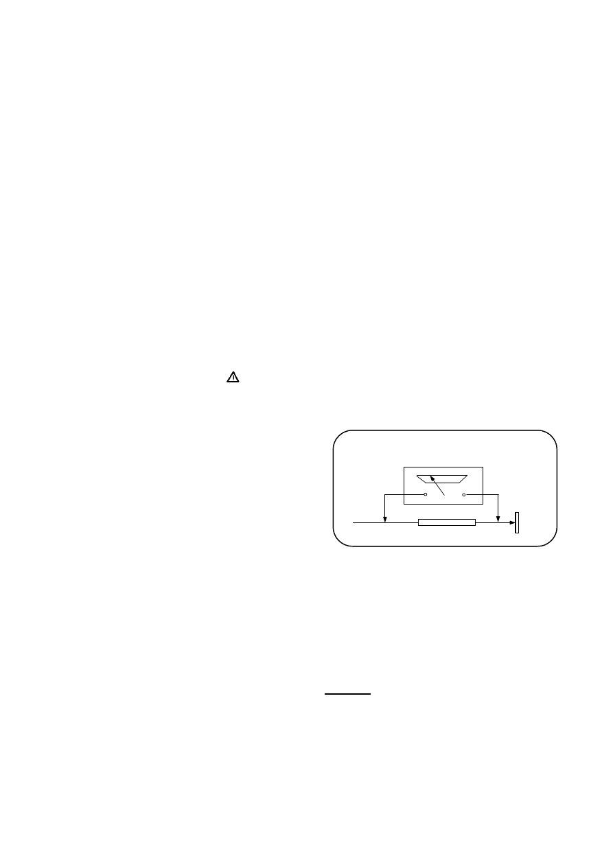
HOT CHECK CIRCUIT
AC-Voltmeter
TO INSTRUMENTS
EXPOSED
METALLIC PARTS
Water pipe
(earth)
2 K Ohm
Figure 1
X-RAY RADIATION WARNING
The primary source of X-ray radiation in this receiver
is the picture tube. The chassis is specially
constructed to limit X-ray radiation. For continued
X-ray radiation protection, replace the tube with
the same type of the original one.
CAUTION
AFTER REMOVAL OF THE ANODE CAP, DISCHARGE
THE ANODE OF THE PICTURE TUBE AND THE ANODE
CAP TO THE METAL CHASSIS, CRT SHIELD, OR THE
CARBON PAINTED ON THE CRT WITH A HIGH
VOLTAGE PROBE AND MULTIMETER (SELECT VDC)
AND THEN SHORT CIRCUIT DIRECTLY TO DISCHARGE
COMPLETELY.

TECHNICAL SPECIFICATIONS
Power source:
220-240V AC, 50-60Hz
Power consumption (max.) : 65 W
14”
85 W
20”, 21”
Standby power consumption :
5 W
Aerial impedance :
75Ohm, coaxial type
Receiving system
1
: PAL
BG
PAL SECAM BG
PAL SECAM BG DK
PAL
I
Receiving channels:
VHF BAND I
CH2-4
VHF BAND III
CH5-12
CABLE
TV
S1-41
UHF
BAND
CH21-69
Audio outputs :
2.0W RMS at %10 THD
14”
2.5W RMS at %10 THD
20”, 21”
High Voltage :
23 ± 0.5 KV
14”
25 ± 0.5 KV
20”, 21”
Focus voltage :
%25.6 ± %38 of EHT
Grid 2 voltage :
0-1400 V
Heater voltage :
6.2 ± 0.2 Vrms
Video/Audio Terminals :
AV1 IN
Video : 1 Vpp,75 Ohm
Audio : 0.5 Vrms, >10 Kohm
RGB
AV1OUT
Video : 1 Vpp, 75 Ohm
Audio : 0.5 Vrms, <1 Kohm
AV2 IN (RCA, optional)
Video : 1 Vpp, 75 Ohm
Audio : 0.5 Vrms, >10 Kohm
Operating temperature :
0-45 Degrees
Safety :
IEC 65 /BS P2N
X-Ray radiation :
ACC. IEC 65/BS P2N
1
: TV set is produced to receive “one” of these colour and sound systems.
Po
w
e
r A
m
plif
ier
TD
A
2822
Au
d
io
ou
t
RG
B
CR
T
Mo
du
le
IC
701
H -
Pu
lse
H-Syn
c
48
49
20/1
3
SI
F 1
-2
44
PI
F
6-7
8
IC101
STV224X
Ho
riz
o
nt
al
Deflect
io
n
BU808DFI
220V
A
C
in
8V
13V
30V
107V
5V
3.
3V
Ve
rt
ic
a
l D
e
fle
c
.
IC
501
TD
A
8174
V-
lin
pin
8
Sc
ar
t
IR
Rece
iv
er
Key
b
o
a
rd
H-s
ync
V-s
ync
EE
PR
OM
IC
402
SCL
O
SD
A
O
Stan
dby
1
28
27
12
19
20
15
24
50
16
IC 401 SDA5552
Microcontroller
CV
BS-T
X
T
R
G
B ou
t +
Fast Blan
ki
ng
AG
C
SC
L
SD
A
IF1
IF
2
Tu
ner P
a
rt
Po
w
e
r S
uppl
y
TD
A
16846
Chassis
12
.8
Block Diagram
R
G
B
out
55
I2
C 51-
52
Bl
a
c
k
33
30-
32
47
42
V-
A
m
p
V
-O
u
t
34-
37
38-
41
Au
d
io
In
/O
u
t
Vi
d
e
o
In
/O
u
t
14/1
1
48/4
9
V-
Sy
n
c
To
IC
40
2
Stan
dby
fro
m
IC
401
PIN VOLTAGES OF IC'S
Pin
Connection
V DC (*)
Pin
Connection
V DC (*)
1 Sound IF Input 1
0.96
29 Not connected
3.20
2 Sound IF Input 2
0.96
30 Blue Output
2.30
3 AGC SIF Capacitor (not connected)
0.22
31 Green Output
2.34
4 IF Voltage Reference Filtering
3.15
32 Red Output
2.48
5 AGC Picture IF Capacitor
2.42
33 Cathode Current Measurement Input
4.17
6 Picture IF Input 1
2.47
34 OSD Blue Input
4.22
7 Picture IF Input 2
2.47
35 OSD Green Input
4.35
8 AGC Tuner Output
2.54
36 OSD Red Input
4.21
9 IF PLL Filter
2.03
37 OSD Fast Blanking
0.31
10 IF Ground
0.00
38 Cloche Filter Tuning Capacitor
0.11
11 AM/FM Mono Sound Output
3.78
39 3.5X MHz Crystal
0.35
12 5 V IF Supply
4.97
40 4.43 MHz Crystal
-
13 Internal CVBS Output
3.00
41 Chroma PLL Filter
-
14 External Audio Input
2.42
42 Vertical Amplitude DAC Output
4.03
15 LC Input 1
3.90
43 Chroma/Scanning Ground
0.00
16 LC Input 2
3.90
44 Second Video Switch Output
4.09
17 Video/Luma Supply Voltage (8 V)
8.05
45 Chroma/Scanning Power Supply (8V)
8.06
18 Internal Video Input
3.63
46 Beam Current Limiter Control Voltage and
Safety Input (XRAY)
6.54
19 Video/Luma Ground
0.00
47 Vertical Output Pulse
5.62
20 External Video Input
3.22
48 Horizontal Output Pulse
1.39
21 Black Stretch Capacitor
2.74
49 Line Flyback Input and Super-sandcastle Output
0.72
22 Y/CVBSIN3 Y(SVHS) or CVBS3 External Input
3.22
50 Scanning PLL Filter
3.98
23 Chroma (SVHS) Input
1.70
51 SCL I2C Bus Clock Input
3.10
24 Automatic RGB Peak Regulation
4.45
52 SDA I2C Bus Data Input
2.80
25 External Blue Input
2.52
53 Digital Supply Voltage (5 V)
5.00
26 External Green Input
1.73
54 Digital Ground
0.00
27 External Red Input
2.52
55 Main Audio Output
3.91
28 External Fast Blanking Input
0.00
56 FM Demodulation Capacitor
1.71
Pin
Connection
V DC
Pin
Connection
V DC
1 Input A +
-
9
Not connected
0.00
2 Not connected
0.00
10 Not connected
0.00
3 Input A -
0.52
11 Output B
5.99
4 Ground
0.00
12 Ground
0.00
5 Ground
0.00
13 Ground
0.00
6 Output A
5.96
14 Input B-
0.52
7 Not connected
0.00
15 Not connected
0.00
8 VCC
12.9 (13.5)
16 Input B -
0.00
IC101 (STV2246)
BUS CONTROLLED MULTISTANDARD ONE CHIP TV PROCESSOR
IC301 (TDA2822) Audio Output IC
Pin
Connection
V DC (*)
Pin
Connection
V DC (*)
1 Standby
0.06 (2.09)
27 SDA I2C Bus Data Input
1.7 (1.93)
2 Not connected
0.80
28 SCL I2C Bus Clock Input
1.7 (1.93)
3 Mute
0.06 (1.62)
29 Ground
0.00
4 LED
1.48 (0.07)
30 VDD 3.3 supply pin
3.30
5 Not connected
0.8 (0.9)
31 Not connected
0.00
6 Not connected
0.8 (0.9)
32 Not connected
3.30
7 Not connected
0.8 (0.9)
33 Reset
3.30
8 Not connected
0.8 (0.9)
34 XTAL2
-
9 VDD 2.5 supply pin
2.46 (2.54)
35 XTAL1
-
10 Ground
0.00
36 Ground
0.00
11 VDD 3.3 supply pin
3.30
37 VDDA 2.5 supply pin
2.41 (2.68)
12 CVBS input for TXT
0.88 (0.99)
38 Red output for OSD and TXT
0.28 (0.0)
13 VDDA 2.5 supply pin
2.41 (2.68)
39 Green output for OSD and TXT
0.28 (0.0)
14 Ground
0.00
40 Blue output for OSD and TXT
0.28 (0.0)
15 Local keyboard input
2.50
41 Fast Blanking for OSD and TXT
0.00
16 Status signal input of Scart pin 8
0.00
42 VDD 2.5 supply pin
2.54
17 Not connected
0.7 (0.8)
43 Ground
0.00
18 Power Ctrl
1.46 (0.24)
44 VDD 3.3 supply pin
3.30
19 Horizontal sync input
2.00 (2.42)
45 Not connected
3.30
20 Vertical sync input
3.13 (3.30)
46 Not connected
0.00
21 Not connected
3.27
47 Not connected
3.28
22 Not connected
3.27
48 SDA I2C Bus for Eeprom
3.28
23 Not connected
3.27
49 SCL I2C Bus Clock for Eeprom
3.28
24 Infra red input
3.27
50 Vertical linearity
0.68
25 AV selection
0.00
51 Not connected
3.28
26 Service
3.27
52 Not connected
3.28
Pin
Connection
V DC
Pin
Connection
V DC
1 Power output
12.55
7
Ramp generator
4.76
2 Output stage Vs
26.78
8
Buffer output
5.68
3 Trigger input
5.41
9
Inverting input
4.48
4 Height adjustment
6.78
10 Vs
26.17
5 Not connected
4.48
11 Flyback generator
1.86
6 Ground
0.00
Pin
Connection
V DC
Pin
Connection
V DC
1 Red in
2.3
6
Vdd supply
191.8
2 Green in
2.3
7
Red out
134-139
3 Blue in
2.4
8
Green out
132-140
4 Gnd
0.0
9
Blue out
127-133
5 Black current output
4.6
IC401 (SDA5552)
MICRO CONTROLLER WITH OSD AND TELETEXT
IC701 TDA6107 RGB Output IC
IC501 (TDA8174) Vertical Deflection Output IC

Pin
Connection
V DC (*)
Pin
Connection
V DC (*)
1 Off time circuit (for standby frequency)
2.91 (2.70)
8
Not connected
-
2 Primary Current Simulation and Startup
1.79 (1.53)
9
Reference Ref. Voltage (5V)
5.59 (5.57)
3 Regulation and Zero Crossing Input
2.17 (0.90)
10 Fault Comparator 1 (not used)
0.00
4 Soft-Start and Regulation Capacitor
3.77 (2.14)
11 Primary Voltage Check
2.61 (2.67)
5 Opto Coupler Input (not connected)
4.64 (4.61)
12 Ground
0.00
6 Fault Comparator 2 (not used)
0.00
13 Output
3.03 (1.06)
7 Synchronization Input (for fixed freq.)
5.59 (5.57)
14 Supply Voltage
13.3 (11.1)
(*)
IC901 (TDA16846) Power Supply IC
Standby measurement values are given in parenthesis
Note:
TV is connected to a patern generator (Colour bar, sound 1 kHz).
IC101 (STV224X)
Pin 37 (OSD On)
1V/div, 20 usn/div, Vpp=2.51 V, 15625 Hz
Pin 44
1V/div, 20 usn/div, Vpp=2.3 V, 15625 Hz
Pin 34 (OSD Off)
1V/div, 20 usn/div, Vpp=1 V, 15625 Hz
Pin 34 (OSD On)
1V/div, 20 usn/div, Vpp=1 V, 15625 Hz
Pin 31
1V/div, 100 usn/div, Vpp=3.7 V, 15625 Hz
Pin 32
1V/div, 100 usn/div, Vpp=4.5 V, 15625 Hz
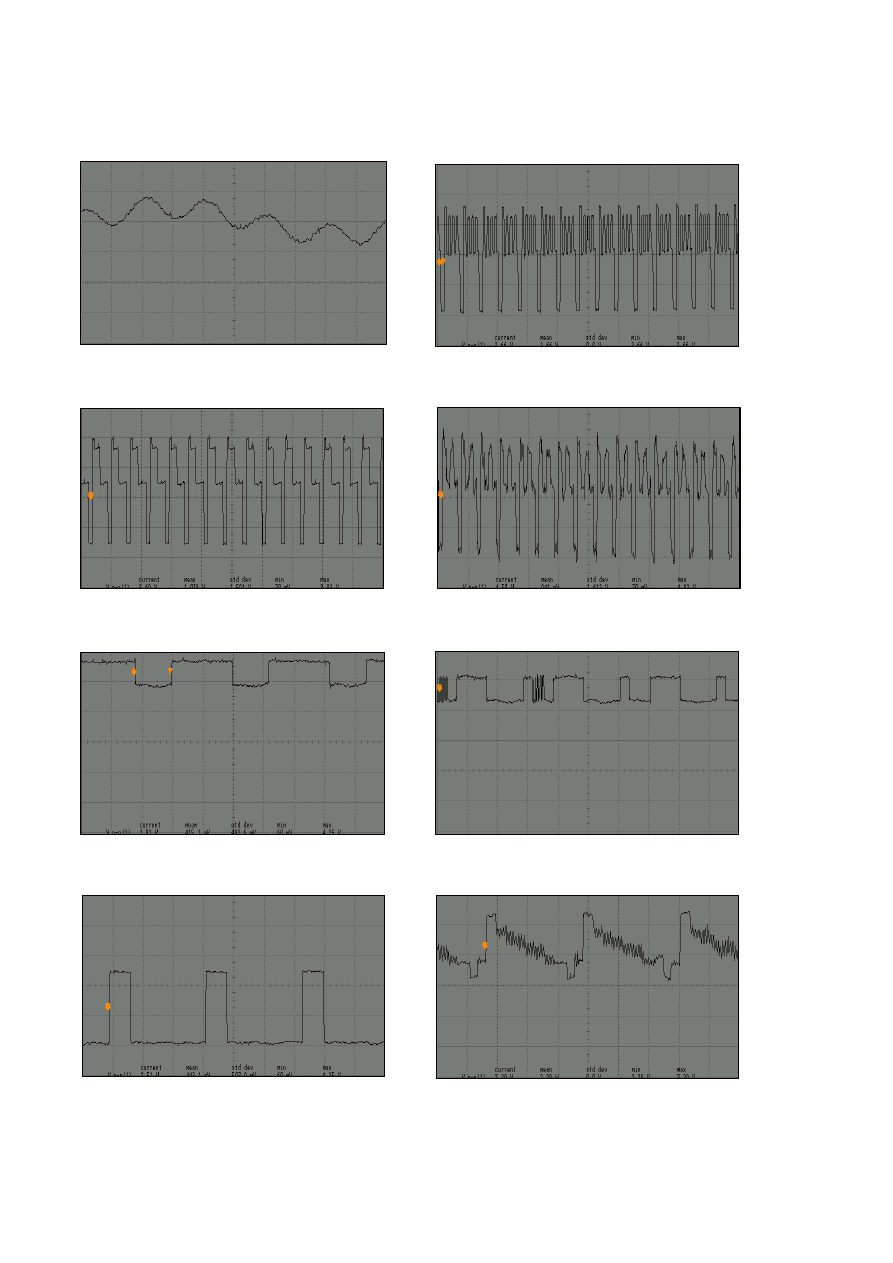
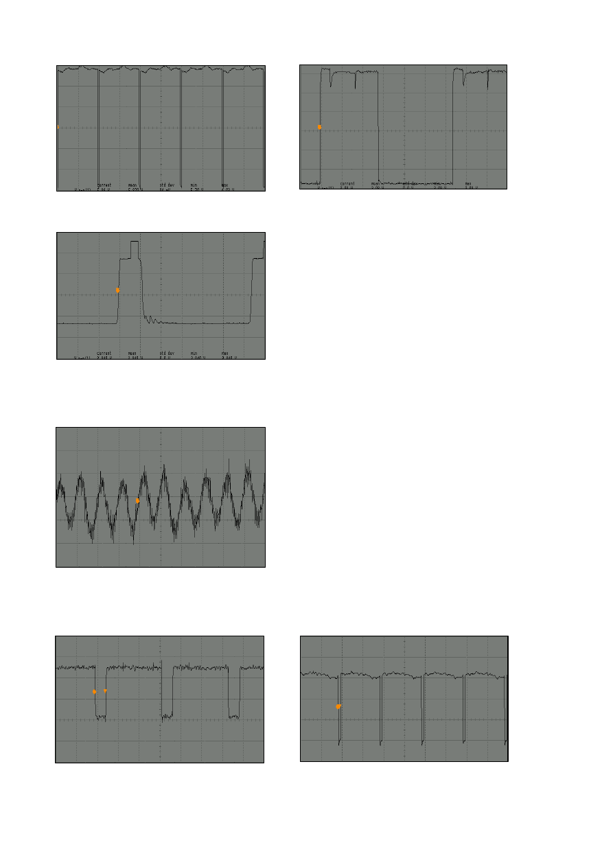
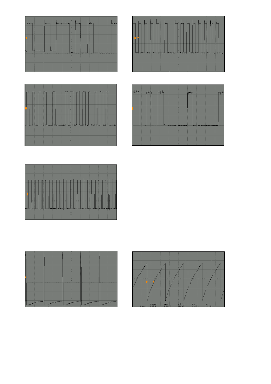
WAVEFORMS OF SOME IC AND TRANSISTOR PINS
Pin 11
1V/div, 100 usn/div, Vpp=1.6 V
Pin 30
1V/div, 100 usn/div, Vpp=3.7 V, 15625 Hz
IC101 (STV224X)
IC301 (TDA2822)
IC401 (SDA5552)
Pin 47
1V/div, 10 msn/div, Vpp=6.0 V, 50 Hz
Pin 48
1V/div, 10 usn/div, Vpp=3.1 V, 15625 Hz
Pin 49
1V/div, 10 usn/div, Vpp=3.9 V, 15625 Hz
Pin 11
50mV/div, 1 msn/div, Vpp=180 mV
Pin 19
1V/div, 20 usn/div, Vpp=3 V
Pin 20
1V/div, 10 msn/div, Vpp=3.6 V, 50 Hz
IC501 (TDA8174)
Pin 27
1V/div, 50 usn/div, Vpp=3.6 V, 10.4 kHz
Pin 28
1V/div, 50 usn/div, Vpp=3.9 V, 31.2 kHz
Pin 7
2V/div, 10 msn/div, Vpp=8.1 V, 50 Hz
Pin 2
5V/div, 10 msn/div, Vpp=26.7 V, 50 Hz
Pin 49
1V/div, 50 usn/div, Vpp=3.6 V, 13.7 kHz
Pin 50
1V/div, 10 usn/div, Vpp=3.7 V, 260 kHz
Pin 48
1V/div, 50 usn/div, Vpp=3.3 V, 31.2 kHz
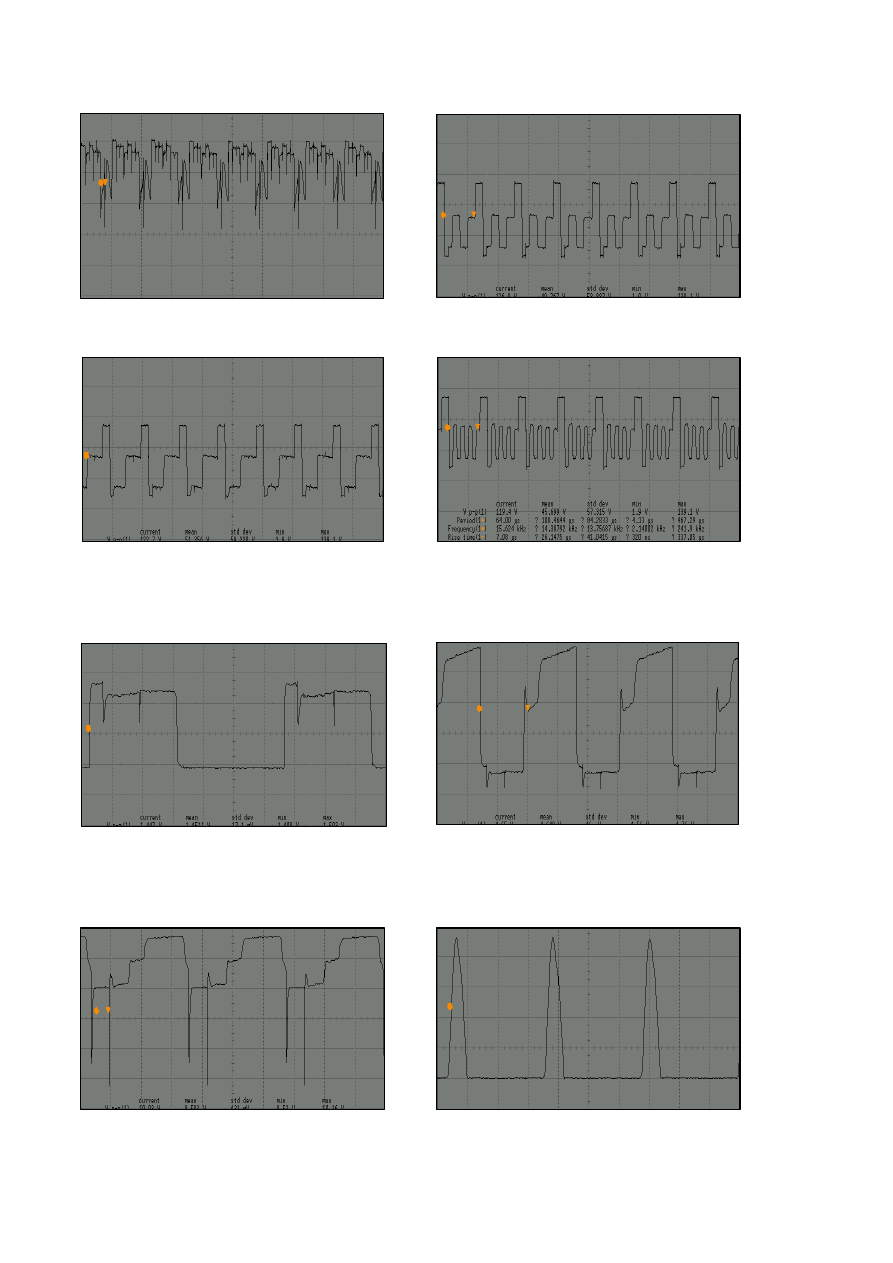
IC701 TDA6107
T551
T552
Pin 5
2V/div, 50 usn/div, Vpp=5.8 V, 15625 Hz
Pin 7
50V/div, 50 usn/div, Vpp=126.8 V, 15625 Hz
Pin 8
50V/div, 50 usn/div, Vpp=122.7 V, 15625 Hz
Pin 9
50V/div, 50 usn/div, Vpp=119.4 V, 15625 Hz
Base
500mV/div, 10 usn/div, Vpp=1.5V, 15625 Hz
Collector
1 V/div, 20 usn/div, Vpp=4.7V, 15625 Hz
Base
Collector
2 V/div, 20 usn/div, Vpp=10V, 15625 Hz
200 V/div, 20 usn/div, Vpp=932V, 15625 Hz
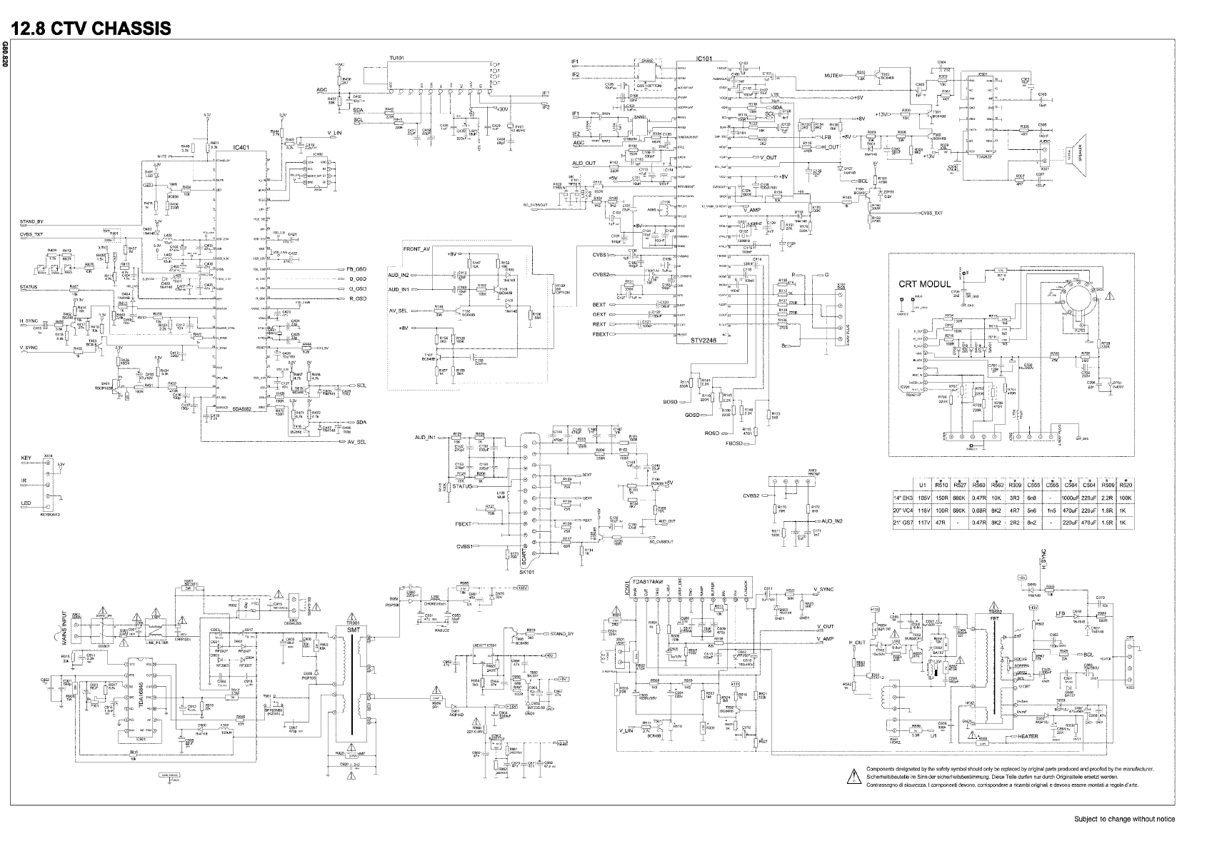
1. ELECTRICAL ADJUSTMENTS
1.1 Supply Voltage Adjustment
Connect a digital voltmeter to the cathode of diode D950 at the AV mode of the TV and set the
screen voltage to the minimum with the screen potentiometer. Adjust the main supply voltage (B+)
with P901 potentiometer to the following value (after supply adjustment, readjust Screen and focus
voltage).
14”
: 105 VDC (for A33EKC01X01)
20”
: 118 VDC (for A48EJW011X21)
21”
: 110 VDC (for A51EFS83X191)
2. SERVICE ADJUSTMENTS
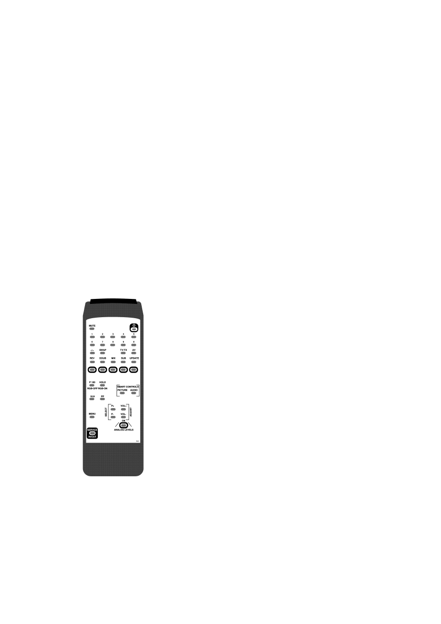
You need the special service remote control to enter and exit the service menu of the TV (you can
order it from the manufacturer). All buttons of the Service RC are same with the user remote control,
only service menu In / Out is added to it (please see the picture below).
Navigation
Service In/Out : Enters to / exits from the Service Menu
P+ / P-
: Moves upward / downward inside the menu
V+ / V-
: Changes the values or options
Red
: for Feature Setup
Green
: for Geometry Adjustments
Yellow
: for White Balance Adjustments
Blue
: for IF adjustment
2.1 IF Adjustments
2.1.1 PAL SECAM BG/DK/I
•
Apply a 38.9 MHz PAL colour bar RF signal to the pin 1 of SAW01 with a pattern generator.
•
Switch on the Service Menu with the Service RC and press “Blue” teletext button.
•
Check that value of “PVC38” is “07”. Adjust the coil LC100 until the the “OK” is seen.
•
Press “OK” button on the Service RC.
•
Exit from the service menu with the Service RC.
Note: “PVF38” is for fine tuning. However, it is automatically applied when “OK” button is pressed
at “PVC38” item. Thus any manual adjustment is not required.

2.1.2 SECAM L/L’
•
“PVC33” and “PVF33” are reserved for Secam LL’. However, since there will be no Secam LL’
production, they would not be adjusted.
2.2 AGC Adjustment
•
Apply a signal with amplitude 65
±
1 dBuV to the antenna input of TV with a pattern generator
(switch sound carrier to Off and switch “Video Ext” to On).
•
Switch on the Service Menu with the Service RC and press “Red” teletext button.
•
Find the “AGC” with P+ / P- buttons.
•
Measure the amplitude of 38.9 MHz sinusoidal signal on pin 11 (IF2) of Tuner with an
oscilloscope.
•
Change “AGC” to get 640
±
20 mVpp.
•
Add 5 to “AGC” value and change “2.AGC” to this value.
•
Exit from the service menu with the Service RC.
2.3 Screen Adjustment
•
Switch on the Service Menu with the Service RC and press “Yellow” teletext button.
•
Find item “SCRN” in the menu.
•
Adjust the Screen potentiometre until the the “OK” is seen.
•
Exit from the service menu with the Service RC.
2.4 White Balance Adjustment
•
Apply a white pattern with a pattern generator to the antenna input.
•
Enter the Service Menu with the Service RC and and press “Yellow” teletext button.
•
Select “G.DRV” option with P+ / P- buttons and change its value to “32” with V+ / V- button.
•
Adjust “R.DRV” and “B.DRV” for white balance. If white balance can not be adjusted properly
change “GRN” value.
•
Adjust “R.CUT” and “G. CUT” for red and green cut off (There is no blue cut off adjustment).
•
Exit from Service menu.
2.5 Geometry Adjustments
•
Apply the cross hatch pattern with a pattern generator to the antenna input.
•
Enter Service Menu with Service RC and press “Green” teletext button.
•
Adjust Vertical Amplitude with “V.4:3” option.
•
Add 18 to ““V.4:3” value and change “V.16:9” to this value.
•
Adjust vertical position with “V.POS”, vertical linearity with “LNRTY”, horizontal position with
“H.POS”.
•
Substract 14 from “V.4:3” value and change “V1. 60” to this value.
•
Add 4 to “V.4:3” value and change “V2. 60” to this value.
•
Change “VP.60” to “V.POS” value.
•
Change “LN.60” to “LNRTY” value.
•
OSD window position can be centered on the screen with “OSD.H” and “OSD.V”.
•
Exit from the Service Menu.
Note that: There is no horizontal width adjustment in this chassis. It can be adjusted by changing
power supply voltage in the interval of -1 and +1 V.
2.6 Feature Setup
Enter the Service Menu with the Service RC and and press “Red” teletext button. Check that below
features match with the set.

TUNER
: Phillips, Sharp&Alps, Panasonic, Temic
ST.BY
: YES (Default, Automatic switch off is active), NO (can be used during repair)
AV2
: YES (Front AV is available), NO
CLR.S
: PAL, PAL/NTSC3.5 (+NTSC Playback), PAL/SECAM, PAL/SECAM/NTSC3.5 (NTSC Pback)
SND.S
: BG, I, BG+DK, BG+LL’
QSS/I
: INTERCARRIER, QSS
TEXT
: NON TEXT, DEFAULT (Teletext), FASTTEXT
OSD CONTR : On (OSD level control is On), Off
LANG
: A (West Europe), B (East Europe)
HOTEL
: NORMAL TV, HOTEL TV
RGBIN
: YES (When RGB on Scart is available, TV can not show aerial signal), NO (Default)
APR
: ON (Auto RGB level control is available) , OFF
B.STR
: ON (Black level control is available), OFF
2.7 Factory Settings for Service Mode
Values given in Table 1 are typical values and can vary according to the CRT type.
14"
20"
21"
AGC
Automatic Gain Control 1
32
32
32
2.AGC
Automatic Gain Control 2
AGC + 5
AGC + 5
AGC + 5
ST.BY Standby
YES YES YES
PVC38
VOC Coarse (BG/I/DK)
07
07
07
PVL38
VCO Fine (BG/I/DK)
68
62
62
PVC33
VOC Coarse (LL')
07
13
13
PVL33
VCO Fine (LL')
64
64
64
APR
Auto RGB level control
ON
ON
ON
B.STR
Black level control
OFF
OFF
OFF
QSS/I QSS/Intercarrier
INTERCARRIER
INTERCARRIER
INTERCARRIER
G.DRV Green
level
32
32
32
R.DRV Red
level
40
40
32
B.DRV Blue
level
37
37
32
R.CUT
Black level offset red
36
36
32
G.CUT
Black level offset green
32
32
32
SCRN
Screen (used for screen adj.)
0
0
0
HPOS Horizontal
shift
30
32
32
VPOS Vertical
shift
12
11
07
V.4:3
Vertical amplitude 4/3 PAL/SEC
23
32
36
V.16:9
Vertical amplitude 16/9 PAL/SEC
V.4:3 + 18
V.4:3 + 18
V.4:3 + 18
LNRTY Vertical
linearity
51
13
49
VP.60
Vertical amplitude NTSC
12
11
07
V1.60
Vertical amplitude 4/3 NTSC
V.4:3 - 14
V.4:3 – 14
V.4:3 – 14
V2.60
Vertical amplitude 16/9 NTSC
V.4:3 + 4
V.4:3 + 4
V.4:3 + 4
LN.60 Linearity
NTSC
51
13
49
OSD.H
OSD Horizontal Shift
31
31
29
OSD.V
OSD Vertical Shift
39
39
38
Table 1
2.8 Exit from Service Menu
During exit from service menu, the software version and feature options (hexadecimal number) are
shown on the screen.
For example: SB7.120-05 BEF9 T02020115

SPARE PARTS LIST
PART NO
NOTES
273471
C-PEM 47NF K 63V R:5
C0001 C0002
201222
CC 220PF K 50V NPO R:5
C0003 C0004
250111
EC 1UF 16V 11*5 R:5
C101
C102
C138
251107
EC 10UF M 16V 11*5 R:5
C105
C127
C134 C140
293230
CC-CHIP 22NF K 50V /0805 X7
C108
C185
294331
CC-CHIP 330NF K 16V /0805 X
C109
292110
CC-CHIP 1NF K 50V /0805 X7R
C110
293474
CC-CHIP 47NF K 50V /0805 X7
C114
C115
C116 C117 C118
294111
CC-CHIP 100NF K 25V /0805 X
C114 C115 C116
292476
CC-CHIP 4.7NF K 50V /0805 X
C128
C129
250227
EC 2.2UF 16V 11*5 R:5
C130
252112
EC 100UF 16V 11*6 R:5
C135
292110
CC-CHIP 1NF K 50V /0805 X7R
C146
C147
C148 C180
291225
CC-CHIP 220PF K 50V /0805 X
C150
C151
C184
291477
CC-CHIP 470PF J 50V /0805 N
C152
C153
291103
CC-CHIP 100PF J 50V /0805 N
C181
C182
C183
251107
EC 10UF M 16V 11*5 R:5
C301
C426
C506
293108
CC-CHIP 10NF K 50V /0805 X7
C303
292223
CC-CHIP 2.2NF K 50V /0805 X
14"
C304
292476
CC-CHIP 4.7NF K 50V /0805 X
20", 21"
C304
294111
CC-CHIP 100NF K 25V /0805 X
C306
C307
252482
EC 470UF 16V 12.5*10 R:5
C308
294231
CC-CHIP 220NF K 16V /0805 X
C401
251478
EC 47UF 16V 11*5 R:5
C402
C405
C407 C415 C430 C433
293108
CC-CHIP 10NF K 50V /0805 X7
C409
C412
291225
CC-CHIP 220PF K 50V /0805 X
C413
291103
CC-CHIP 100PF J 50V /0805 N
C416
C428
292223
CC-CHIP 2.2NF K 50V /0805 X
C418
250227
EC 2.2UF 16V 11*5 R:5
C419
290334
CC-CHIP 33PF J 50V /0805 NP
C424
C425
252229
EC 220UF 16V 11*8 R:5
C430
290222
CC-CHIP 22PF J 50V /0805 NP
C431
C432
290684
CC-CHIP 68PF J 50V /0805 NP
C438
274227
C-PEM 220NF J 50V R:5
C501
253106
EC 1000UF 25V 20*13 R:5
C503
253101
EC 1000UF 35V 25*13 R:5
C503
252476
EC 470UF 25V 11*10 R:5
21"
C504
250111
EC 1UF 16V 11*5 R:5
C505
C511
C512
293152
CC-CHIP 15NF K 50V /0805 X7
C508
273333
C-PEM 33NF K 100V R:5
C508A
291477
CC-CHIP 470PF J 50V /0805 N
C509
252105
EC 100UF 50V 12*8 R:5
C510
294109
CC-CHIP 100NF K 50V /0805 X
C513
C562
250100
EC 1UF 160V 11*6.3 R:5
C553
271390
C-PPM 390NF J 250V R:15
C554
272687
C-PPM 6.8NF %3.5 1.5/1.6KV
14"
C555
272820
C-PPM 8.2NF %3.5 1.5/1.6KV
21"
C555
274330
C-PEM 330NF J 250V R:15
C556
251109
EC 10UF 250V 16*10 R:5
C560
202105
CC 1NF K 1KV Y5P R:5
C561
274107
C-PEM 100NF J 100V R:5
C563
252229
EC 220UF 16V 11*8 R:5
21"
C564
252482
EC 470UF 16V 12.5*10 R:5
20"
C564
272154
C-PPM 1.5NF J 1600V R:15
C565
293108
CC-CHIP 10NF K 50V /0805 X7
C570
290473
CC-CHIP 47PF J 50V /0805 NP
C701
C706
C709
274105
C-PEM 100NF J 250V R:10
C701
C713
251109
EC 10UF 250V 16*10 R:5
C702
C703
291225
CC-CHIP 220PF K 50V /0805 X
C703
C707
C710
DESCRIPTION
POSITION NUMBERS

SPARE PARTS LIST
PART NO
NOTES
273225
C-PEM 22NF J 63V R:5
C704
202221
C-CE 2.2NF K 2KV Y5P R:7.5
C705
C712
201476
C-CE 470PF K 1KV R:5
C705
C708
C711
274103
C-PEM 100NF K 275V-AC R:15
C901
274224
C-PEM 220NF K 275V-AC R22.
C901
251120
EC 10UF 10V 5*4 R:5
C901
274103
C-PEM 100NF K 275V-AC R:15
C902
202105
CC 1NF K 1KV Y5P R:5
C903
C904
203330
C-PPM 33NF J 630V R:15
C906
201471
CC 470PF 2KV
C907
292223
CC-CHIP 2.2NF K 50V /0805 X
C913
292151
CC-CHIP 1.5NF K 50V /0805 X
14", 21"
C914
292223
CC-CHIP 2.2NF K 50V /0805 X
20"
C914
274105
C-PEM 100NF J 250V R:10
C915
273222
C-PEM 22NF K 250V R:7.5
C915
202220
CC 2.2NF M 250VAC Y5U R:10
C920
291560
CC-CHIP 560PF J 50V /0805 N
C921
290561
CC-CHIP 56PF J 50V NPO 0805
C923
201226
CC 220PF K 2KV Y5P R:5
C950
253106
EC 1000UF 25V 20*13 R:5
C954
251107
EC 10UF M 16V 11*5 R:5
C966
251478
EC 47UF 16V 11*5 R:5
C968
291101
CC-CHIP 100PF J 50V /1206 N
C981
C982
179002
RC-CHIP 0R /1206
D103
302289
DIODE 1N4148 52MM
D105
D106
303195
DIODE 4148 MELF
D105
D106
D107
302296
DIODE 1N4148 26MM
D110
303850
LED LTL 4263 RED L=25.4
D401
303988
LED LTL 4224 RED (SHORT LEG
D401
302296
DIODE 1N4148 26MM
D402
D403
D404 D406 D407
302289
DIODE 1N4148 52MM
D402
D403
D404 D406 D407
303308
DIODE RF2007
D502
302289
DIODE 1N4148 52MM
D503
D557
D558 D559
303195
DIODE 4148 MELF
D503
D557
300305
DIODE BA157
D552
D556
D560
303227
DIODE RGP15J
D553
302948
DIODE 1N4007
D701
302296
DIODE 1N4148 26MM
D702
D703
D704
303209
DIODE BAV21
D702
D703
D704
303308
DIODE RF2007
D901
D902
D903 D904
303244-01
DIODE RGP30K(GENERAL SEMI C
D901
D902
D903 D904
303206-01
DIODE RGP30M (GENERAL SEMI
D901
D902
D903 D904
303214
DIODE UF4006
D901
D902
D903 D904
303217
DIODE RGP10J
D905
303227
DIODE RGP15J
14"
D950
303244
DIODE RGP30K
20", 21"
D950
303813
DIODE RGP15D
D951
303993
LED LTL4221N D:3 R/D RED
D980
303991
LED IR SIR563SB3F 23/940
D981
056722
SER.FILTER TPS5.5MB
BG
F102
056745
SER.FILTER TPS6.0MB
I
F102
056762
SER.FILTER TPT02B
BG/DK
F102
056640-01
SER.FILTER MKT40.4MA110P-TF
F401
452842
IC STV2246-5X
PAL BG, I SYSTEMS
IC101
452990
IC STV2249C
PAL/SEC BG/DK SYSTEM
IC101
452439
IC TDA2822
IC301
DESCRIPTION
POSITION NUMBERS
SPARE PARTS LIST
PART NO
NOTES
452807
IC SDA555XFL
IC401
452837
IC-CHIP BR24C04 (SOP8)
IC402
452648
IC TDA8174AW
IC501
452746
IC TDA6107Q
IC701
452795
IC TDA16846
IC901
451518
IC KA317TU T0220CASE
IC951
IC952
452382
IC-CHIP S3C1840DA9/SMB1
IC980
055139
CHOKE COIL 50MHZ 600R PH-WB
L0001
L0002
053725
COIL-CHIP 10UH %20/0805
L101
L102
052828
COIL 6.8UH K R:5
L103
053740
COIL 1UH K LAL03
L104
053798
COIL-CHIP 18UH K /0805
L109
053749
COIL 18UH K /3.4 26MM
L401
053711
COIL 10UH K (TAIYO) LAL03
L402
L403
L404
053715
COIL 6.8UH K R12.5
L502
051591
COIL H-LIN 55UH NEOSID
21"
L551
051585
COIL H-LIN 70UH
14", 20"
L551
053352
COIL- CHOKE 10UH R0814 14.1
L701
051687-02
LINE FILTER 27MH E-TYPE OPE
L901
053759
COIL 100UH LAL03
L902
053739
COIL CHOKE 50UH
L950
053506-01
COIL DEMOD 38.9 HEX
LC100
179001
RC-CHIP 0R /0805 2*1.25
LK501
132209
R-VAR 2.2K (V) 5*3
14"
P901
132500
R-VAR 5K (V) 5*3
20", 21"
P901
056023
CRYSTAL 4.433619MHZ (NO LOA
Q101
056660
CRYSTAL 3.579545 90OHM BULK
Q102
056620
CRYSTAL 6MHZ (CL 30PF)
Q401
056210
CER.RESONATOR GSB455E
Q980
101221
CFR 220R J 1/2W 52MM
R0001
R0003
173273
CFR-CHIP 27K J 1/10W /0805
R101
171150
RC-CHIP 150R J 1/10W /0805
R102
R113
172152
RC-CHIP 1.5K J 1/10W /0805
R104
R105
173684
RC-CHIP 68K J 1/10W /0805
R106
174180
RC-CHIP 180K J 1/10W /0805
R108
171221
RC-CHIP 220R J 1/10W /0805
R109
R110
R111 R142
172101
RC-CHIP 1K J 1/10W /0805
R112
172561
RC-CHIP 5.6K J 1/10W /0805
R115
R123
R172
171471
RC-CHIP 470R J 1/10W /0805
R116
170683
RC-CHIP 68R J 1/10W /0805
R117
171102
RC-CHIP 100R J 1/10W /0805
R120
R151
R152
173154
RC-CHIP 15K J 1/10W /0805
R122
R124
R125
170750
RC-CHIP 75R J 1/10W /0805
R126
R127
R128 R129 R155
173562
RC-CHIP 56K J 1/10W /0805
R130
174331
RC-CHIP 330K J 1/10W /0805
R131
R175
R176
172225
RC-CHIP 2.2K J 1/10W /0805
R132
R133
R144 R145 R146
172823
RC-CHIP 8.2K J 1/10W /0805
R134
171270
RC-CHIP 270R J 1/10W /0805
R135
R136
R137
173479
RC-CHIP 47K J 1/10W /0805
R138
173101
RC-CHIP 10K J 1/10W /0805
R139
174104
RC-CHIP 100K J 1/10W /0805
R141
R149
R171
173333
RC-CHIP 33K J 1/10W /0805
R148
172475
RC-CHIP 4.7K J 1/10W /0805
R154
102141
CFR 1K J 1/4W /6 26MM
AV
R157
R568
179001
RC-CHIP 0R /0805 2*1.25
R159
DESCRIPTION
POSITION NUMBERS

SPARE PARTS LIST
PART NO
NOTES
171332
RC-CHIP 330R J 1/10W /0805
R180
R205
R206
171471
RC-CHIP 470R J 1/10W /0805
R181
171685
RC-CHIP 680R J 1/10W 0805
R184
172475
RC-CHIP 4.7K J 1/10W /0805
20", 21"
R301
172335
RC-CIHP 3.3K J 1/10W /0805
14"
R301
173154
RC-CHIP 15K J 1/10W /0805
R302
173333
RC-CHIP 33K J 1/10W /0805
R303
R308
172823
RC-CHIP 8.2K J 1/10W /0805
R304
173101
RC-CHIP 10K J 1/10W /0805
R305
170047
RC-CHIP 4.7R J 1/10W /0805
R306
R307
119331
RMF 3.3R J 1W
14"
R309
119485
RMF 4.7R J 1.5W
20", 21"
R309
172335
RC-CIHP 3.3K J 1/10W /0805
R401
173101
RC-CHIP 10K J 1/10W /0805
R404
R414
R418
172101
RC-CHIP 1K J 1/10W /0805
R405
R413 R422 R423
171270
RC-CHIP 270R J 1/10W /0805
R406
175102
RC-CHIP 1M J 1/10W /0805
R407
172152
RC-CHIP 1.5K J 1/10W /0805
R408
R409
171685
RC-CHIP 680R J 1/10W 0805
R410
172475
RC-CHIP 4.7K J 1/10W /0805
R411
R412 R467 R468
172561
RC-CHIP 5.6K J 1/10W /0805
R415
R416
173273
CFR-CHIP 27K J 1/10W /0805
R417
171150
RC-CHIP 150R J 1/10W /0805
R425
102338
CFR 3.3K J 1/4W /6 52MM
R434
R446
172273
RC-CHIP 2.7K J 1/10W /0805
R436
R511
173393
RC-CHIP 39K J 1/10W /0805
R437
171221
RC-CHIP 220R J 1/10W /0805
R441
R442
172823
RC-CHIP 8.2K J 1/10W /0805
R445
R464
173154
RC-CHIP 15K J 1/10W /0805
R447
172394
RC-CHIP 3.9K J 1/10W /0805
R448
R524
179001
RC-CHIP 0R /0805 2*1.25
R478
119227-01
RMF 2.2R J 1W
R501
101471
CFR 470R J 1/2W /9 52MM
R502
R557
100220
CFR 22R J 1/2W 52MM
R503
172101
RC-CHIP 1K J 1/10W /0805
R504
R552
174151
RC-CHIP 150K J 1/10W /0805
R505
R506
172183
RC-CHIP 1.8K J 1/10W /0805
R508
R512
119125
RM 1.2R J 1/2W 52MM
21"
R509
119153
RM 1.5R J 1/2W 52MM
20"
R509
170472
RC-CHIP 47R J 1/10W /0805
21"
R510
171150
RC-CHIP 150R J 1/10W /0805
14"
R510
102141
CFR 1K J 1/4W /6 26MM
R519
R568
172101
RC-CHIP 1K J 1/10W /0805
20", 21"
R520
174104
RC-CHIP 100K J 1/10W /0805
R521
173562
RC-CHIP 56K J 1/10W /0805
R522
R523
173221
RC-CHIP 22K J 1/10W /0805
R526
110823
RMO 82R J 3W R:20
R554
100473
CFR 47R J 1/4W /6 52MM
R555
113114
RM 10K J 1/2W 52MM
R558
119337
RMO 3.3R J 2W R:27.5 TAPE
R559
119478
RMF 0.47R J 1W
14", 21"
R560
119684
RMF 0.68R J 1W
20"
R560
103116
CFR 10K J 1/4W /6 52MM
R562
103136
CFR 10K J 1/4W /6 26MM
14"
R563
171560
RC-CHIP 560R J 1/10W /0805
R564
103475
CFR 47K J 1/4W /6 52MM
R705
102159
CFR 1.5K J 1/2W /9 52MM
R711
R713
R715 R716 R725
171471
RC-CHIP 470R J 1/10W /0805
R711
R716
R721
171102
RC-CHIP 100R J 1/10W /0805
R712 R717
DESCRIPTION
POSITION NUMBERS
SPARE PARTS LIST
PART NO
NOTES
154216
NTC 5.1R M (S234R)
R901
113683
RMO 68K J 1.5W 73MM
R903
115103
RM 1M J 1W 52MM
R908
115391
RM 3.9M J 1W 52MM
R912
173333
RC-CHIP 33K J 1/10W /0805
R915
R918
172683
RC-CHIP 6.8K J 1/10W /0805
R917
115470
RM 4.7M J 1/2W 52MM
R920
113180
RMO 18K J 1W
R950
171240
RC-CHIP 240R %1 1/10W /0805
R953
R961
112131
RM 1.3K %1 1/4W 26MM
R954A
109560
CFR 5.6R J 1/4W /3.2 52MM
R956
101106
CFR 100R J 1/4W 52MM
R957
119109
RNF 0.1R J 0.4W (UFLB) 52MM
R959
120234
RMF 22R J 1/2W
R960
171394
RC-CHIP 390R %1 1/10W /0805
R962
179002
RC-CHIP 0R /1206
R981
452521
IR RECEIVER TSOP 1838
S401
054261
FUSE 2.5AT (215 SER.)
S901
056746
SAW FILTER OFW G1968M
BG SYSTEM
SAW01
056760
SAW FILTER OFW J1956M
I SYSTEM
SAW01
056070
SAW FILTER OFW K2966M
BG/DK SYSTEM
SAW01
031229
SCART SOCKET 11.1
SK101
010860
TACT SW LONG STEN
SW401 SW402 SW403
010861
ON/OFF SWITCH BK98
SW901
401141
TRN-CHIP BC848B SOT23
T101
T102
T107
401141
TRN-CHIP BC848B SOT23
T301
T302 T303
401142
TRN-CHIP BC858B SOT23
T401
401141
TRN-CHIP BC848B SOT23
T501
T502
401334
TRN STX112
T551
401332
TRN BU808DFI
T552
400338
TRN BF422
T701
T703
T705
401366
TRN BF421
T702
T704
T706
401219
TRN STP3NB60FP
T901
401047
TRN BC337-25
T950
401142
TRN-CHIP BC858B SOT23
T980
058013-TR1
DST 2021/MS TR/003071083 12
20", 21"
TR552
58413
FBT-SANAL 14" 12.1
14"
TR552
59013
SMPS-SANAL 20/21" 12.1
20", 21"
TR901
59413
SMPS-SANAL 14" 12.1
14"
TR901
7RZ136-PH3
TUNER PH ASIMETRIK UV1316/A
TU101
031176
CONN.CINCH 12.1 FRONT-AV YE
X0002
031162
KONN. CINCH RCA PJ803-4 YEL
X0002
031166
CONN.CINCH 12.1 FRONT-AV WH
X0003
031160
KONN. CINCH RCA PJ803-2 WHI
X0003
031180
CONN.HEADPHONE 12.1 FRONT-A
X0004
031856
CONN.HOUSING X2003 BLACK
X301
031860
CONN.HOUSING X2004 BLACK
X403
031864
CONN.HOUSING X2005 BLACK
X404
031780
CONN.HOUSING 2'LI GREY
X501
031777
CON.HOUSING LOCKED 5/4
X551
031532
CRT SOCKET NARROW INCHANG
14"
X703
031530-01
INCHANG/CRT SOCKET ISHM05S-
20", 21"
X703
031675
CON.HOUSING 2P MALE
X901
X902
302786
DIODE Z. MTZJ6.2B
ZD101
303771
DIODE Z. UZT33V
ZD570
DESCRIPTION
POSITION NUMBERS

SPARE PARTS LIST
303735
MTZJ5.6B
ZD952
056314-EK3
CPT EK A33EKC01X01
14"
056321-GS7
CPT GS A51QAE320X67 (WALES)
21"
056320-VC1
CPT VC A48EJW011X21
20"
614167-AS
DEGAUSSING COIL ASSY 14" BA
14"
620167-AS
DEGAUSSING COIL ASSY 20" BA
20"
621167-AS
DEGAUSSING COIL ASSY 21" BA
21"
B25187
R.CONTROL SILVER PAINTED B-
C29187
RC A.TYPE SILVER PAINTED
M93187
RC B.TYPE YLG PAINTED 12.4/
6BZ107-AS
SPEAKER SM 16R/3W
5FZ107-AS
SPEAKER SM 8R/3W NOM.50*90
Please note that Product Part List Files should be investigated for the mechanical parts like cabinets, etc.


ROADSTAR MANAGEMENT SA.
(INTERNATIONAL SERVICE DIVISION)
Via Passeggiata, 1 - BALERNA - SWITZERLAND
Tel. +4191-6975155 - Fax. +4191-6975151
e-mail: aftersal@roadstar.com
ROADSTAR ITALIA S.P.A.
SERVICE DIVISION (DOMESTIC ITALY)
Viale Matteotti, 22 - CERNOBBIO (CO) -ITALY
Tel. +39031-342340 - Fax. +39031-3346291
Wyszukiwarka
Podobne podstrony:
BEKO chassis 12 3 01
beko chassis 12 7 schematics
BEKO chassis 12 4 01
BEKO chassis 12 3 02
beko chassis 12 1 schematics
12 04 86
newsletter 12 04
1995 12 04 2796
gazeta podatkowa nr 102 z 30 12 04 5IPSDBY25FT6RHAT4YXBEXTW3MYM5PGWJUOYT4Y
12-04 lokalna oferta finansowania zewnetrznego, Analiza ekonomiczna przedsiębiorstwa
Wyklad 12.04.2012, Biologia, zoologia
12 04 4N6BNORMNSCQJ2FXXOG26LZFWKZMWPQ5D36SNIY
Kwiecień, Ekologistyka 12.04
Kwiecień, Ekologistyka 12.04
12-04-2013, Anatomia
12 04 27 chkol2
12 04
Ekonnomia Wykład 6 12 04 2013
2008 12 04 (4)
więcej podobnych podstron