5895
8-BIT SERIAL-INPUT,
LATCHED DRIVERS
BiMOS II 8-BIT SERIAL INPUT,
LATCHED SOURCE DRIVERS
The UCN5895A, UCN5895EP, and A5895SLW BiMOS II serial-
input, latched source drivers are designed for applications emphasiz-
ing low output saturation voltages and currents to -250 mA per output.
These smart high-side octal, driver ICs merge an 8-bit CMOS shift
register, associated CMOS latches, and CMOS control logic (strobe
and output enable) with medium current emitter-follower (sourcing)
outputs. Typical applications include incandescent or LED displays
(both directly driven and multiplexed), non-impact (i.e., thermal)
printers, relays, and solenoids.
Each device is suitable for high-side applications to -250 mA per
channel. The maximum supply voltage is 50 V and a minimum output
sustaining voltage rating of 35 V for inductive load applications. Under
normal operating conditions, the UCN5895A and UCN5895EP are
capable of providing -120 mA (8 outputs continuous and simultaneous)
at +65
°
C with a logic supply of 5 V. Similar devices, with higher output
current ratings, are the UCN5890A and UCN5891A.
BiMOS II devices can operate at greatly improved data-input rates.
With a 5 V supply, they will typically operate at better than 5 MHz.
At 12 V, significantly higher speeds are obtained.
The CMOS inputs provide for minimum loading and are compatible
with standard CMOS, PMOS, and NMOS circuits. TTL or DTL circuits
may require the use of appropriate pull-up resistors to ensure a proper
input-logic high. A CMOS serial data output allows cascading these
devices in multiple drive-line applications required by many dot matrix,
alphanumeric, and bar graph displays.
These devices are rated for continuous operation over the tem-
perature range of -20
°
C to +85
°
C. Because of limitations on package
power dissipation, the simultaneous operation of all output drivers may
require a reduction in duty cycle. The UCN5895A is supplied in a
standard 16-pin dual in-line plastic package with a copper lead frame
for increased allowable package power dissipation. The UCN5895EP
is supplied in a 20-lead plastic leaded chip carrier for minimum area,
surface-mount applications. The A5895SLW is supplied in a 16-lead
wide-body plastic SOIC.
FEATURES
■
Low Output-Saturation Voltage
■
Source Outputs to 50 V
■
Output Current to -250 mA
■
To 3.3 MHz Data-lnput Rate
■
Low-Power CMOS Logic & Latches
Always order by complete part number, e.g.,
UCN5895A .
UCN5895A
Data Sheet
26182.14B*
Note the UCN5895A (DIP) and the A5895SLW
(SOIC) are electrically identical and share a common
terminal number assignment.
ABSOLUTE MAXIMUM RATINGS
at T
A
= +25
°
C
Output Voltage, V
OUT
. . . . . . . . . . . . . . 50 V
Logic Supply Voltage Range,
V
DD
. . . . . . . . . . . . . . . . . . 4.5 V to 12 V
Driver Supply Voltage Range,
V
BB
. . . . . . . . . . . . . . . . . . 5.0 V to 50 V
Input Voltage Range,
V
IN
. . . . . . . . . . . -0.3 V to V
DD
+ 0.3 V
Continuous Output Current,
I
OUT
. . . . . . . . . . . . . . . . . . . . . -250 mA
Allowable Package Power Dissipation,
P
D
. . . . . . . . . . . . . . . . . . . . See Graph
Operating Temperature Range,
T
A
. . . . . . . . . . . . . . . . . -20
°
C to +85
°
C
Storage Temperature Range,
T
S
. . . . . . . . . . . . . . . . -55
°
C to +150
°
C
Caution: CMOS devices have input-static
protection, but are susceptible to damage when
exposed to extremely high static electrical
charges.
5895
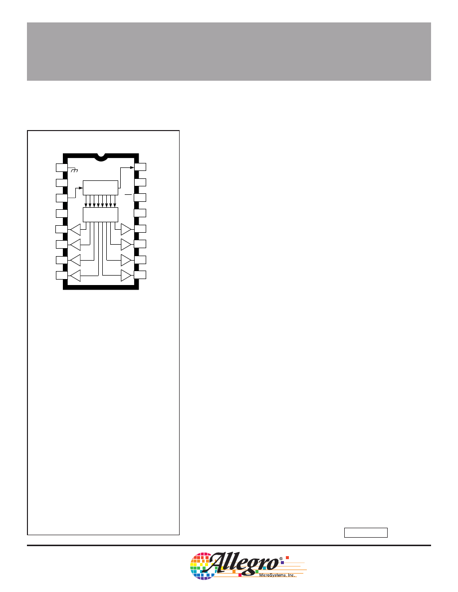
2
3
4
5
6
7
8
SERIAL
DATA OUT
SERIAL
DATA IN
OUTPUT
ENABLE
LOGIC
SUPPLY
STROBE
CLOCK
CLK
V
DD
ST
OE
1
GROUND
9
10
11
12
13
14
15
16
OUT
1
OUT
2
OUT
3
Dwg. PP-026-2A
OUT
5
OUT
6
OUT
7
OUT
8
OUT
4
SHIFT
REGISTER
LATCHES
V
BB
LOAD
SUPPLY
5895
8-BIT SERIAL-INPUT,
LATCHED DRIVERS
115 Northeast Cutoff, Box 15036
Worcester, Massachusetts 01615-0036 (508) 853-5000
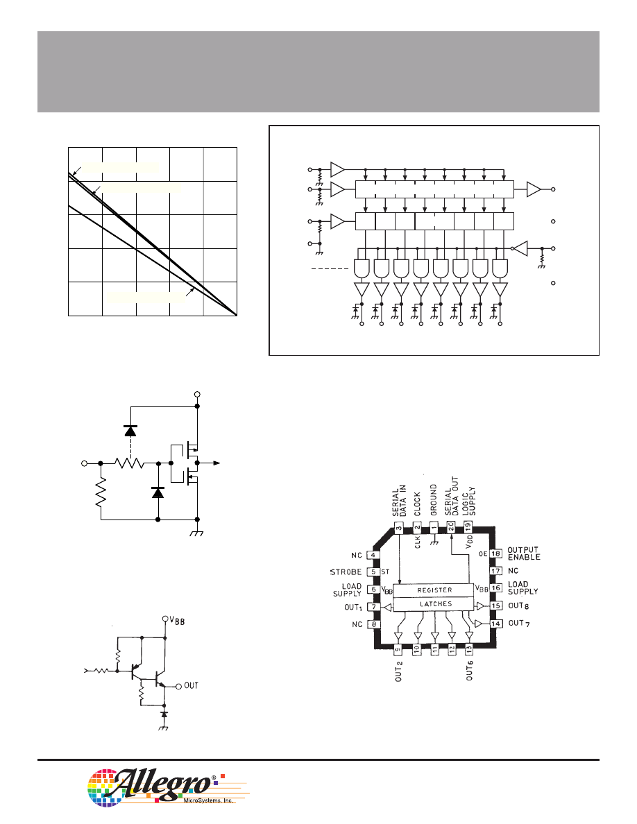
8-BIT SERIAL-PARALLEL SHIFT REGISTER
GROUND
STROBE
SERIAL
DATA IN
CLOCK
LATCHES
MOS
BIPOLAR
VBB
SERIAL
DATA OUT
VDD
OUTPUT
ENABLE
OUT1 OUT2 OUT3 OUT4 OUT5 OUT6 OUT7 OUT8
TYPICAL INPUT CIRCUIT
FUNCTIONAL BLOCK DIAGRAM
Dwg. No. A-12,654
Dwg. No. A-12,655
Dwg. EP-010-4A
IN
V
DD
Dwg. No. A-14,368
UCN5895EP
Copyright © 1985, 1999, Allegro MicroSystems, Inc.
50
75
100
125
150
2.5
0.5
0
ALLOWABLE PACKAGE POWER DISSIPATION IN WATTS
AMBIENT TEMPERATURE IN
°
C
2.0
1.5
1.0
25
SUFFIX 'A', R = 60
°
C/W
θ
JA
SUFFIX 'EP', R = 59
°
C/W
θ
JA
Dwg. GP-024-4
SUFFIX 'LW', R = 80
°
C/W
θ
JA
TYPICAL OUTPUT DRIVER
5895
8-BIT SERIAL-INPUT,
LATCHED DRIVERS
ELECTRICAL CHARACTERISTICS at T
A
= +25
°
C, V
BB
= 50 V, V
DD
= 5 V and 12 V
(unless otherwise noted).
Limits
Characteristic
Symbol
Test Conditions
Min.
Max.
Units
Output Leakage Current
I
OUT
T
A
= +25
°
C
—
-50
µ
A
T
A
= +70
°
C
—
-100
µ
A
Output Saturation Voltage
V
CE(SAT)
I
OUT
= -60 mA
—
1.1
V
I
OUT
= -120 mA
—
1.2
V
Output Sustaining Voltage
V
CE(sus)
I
OUT
= -120 mA, L = 2 mH
35
—
V
Input Voltage
V
IN(1)
V
DD
= 5.0 V
3.5
5.3
V
V
DD
= 12 V
10.5
12.3
V
V
IN(0)
V
DD
= 5 V to 12 V
-0.3
+0.8
V
Input Current
I
IN(1)
V
DD
= V
IN
= 5.0 V
—
50
µ
A
V
DD
= V
IN
= 12 V
—
240
µ
A
Input lmpedance
z
IN
V
DD
= 5.0 V
100
—
k
Ω
V
DD
= 12 V
50
—
k
Ω
Max. Clock Frequency
f
CLK
3.3
—
MHz
Serial Data-Output
r
OUT
V
DD
= 5.0 V
—
20
k
Ω
V
DD
= 12 V
—
6.0
k
Ω
Turn-ON Delay
t
PLH
Output Enable to Output, I
OUT
= -120 mA
—
2.0
µ
s
Turn-OFF Delay
t
PHL
Output Enable to Output, I
OUT
= -120 mA
—
10
µ
s
Supply Current
I
BB
All outputs ON, All outputs open
—
10
mA
All outputs OFF
—
200
µ
A
I
DD
V
DD
= 5 V, All outputs OFF, Inputs = 0 V
—
100
µ
A
V
DD
= 12 V, All outputs OFF, Inputs = 0 V
—
200
µ
A
V
DD
= 5 V, One output ON, All inputs = 0 V
—
1.0
mA
V
DD
= 12 V, One output ON, All inputs = 0 V
—
3.0
mA
Diode Leakage Current
I
R
V
R
= 25 V, T
A
= +25
°
C
—
50
µ
A
V
R
= 25 V, T
A
= +70
°
C
—
100
µ
A
Diode Forward Voltage
V
F
I
F
= 120 mA
—
2.0
V
Resistance
5895
8-BIT SERIAL-INPUT,
LATCHED DRIVERS
115 Northeast Cutoff, Box 15036
Worcester, Massachusetts 01615-0036 (508) 853-5000
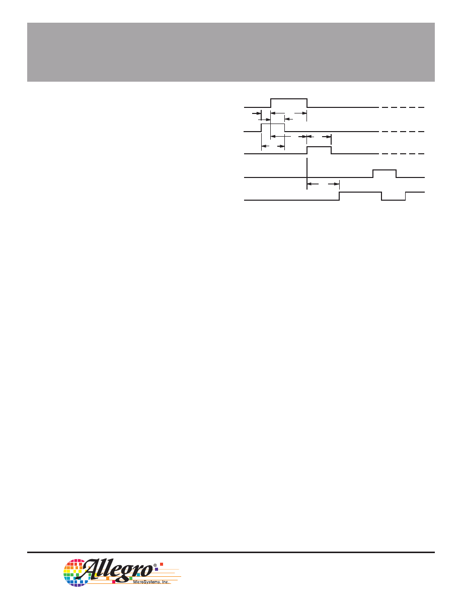
TIMING CONDITIONS
(V
DD
= 5.0 V, Logic Levels are V
DD
and Ground)
A.
Minimum Data Active Time Before Clock Pulse
(Data Set-Up Time) ................................................................. 75 ns
B.
Minimum Data Active Time After Clock Pulse
(Data Hold Time) ..................................................................... 75 ns
C.
Minimum Data Pulse Width ........................................................ 150 ns
D.
Minimum Clock Pulse Width ...................................................... 150 ns
E.
Minimum Time Between Clock Activation and Strobe ............... 300 ns
F.
Minimum Strobe Pulse Width ..................................................... 100 ns
G.
Typical Time Between Strobe Activation and
Output Transition .................................................................... 1.0
µ
s
Serial Data present at the input is transferred to the shift register
on the logic “0” to logic “1” transition of the CLOCK input pulse. On
succeeding CLOCK pulses, the registers shift data information towards
the SERIAL DATA OUTPUT. The SERIAL DATA must appear at the
input prior to the rising edge of the CLOCK input waveform.
Information present at any register is transferred to its respective
latch when the STROBE is high (serial-to-parallel conversion). The
latches will continue to accept new data as long as the STROBE is
held high. Applications where the latches are bypassed (STROBE tied
high) will require that the OUTPUT ENABLE input be high during serial
data entry.
When the OUTPUT ENABLE input is high, all of the output buffers
are disabled (OFF) without affecting the information stored in the
latches or shift register. With the OUTPUT ENABLE input low, the
outputs are controlled by the state of their respective latches.
Dwg. No. A-12,649A
E F
CLOCK
DATA IN
STROBE
BLANKING
OUT
N
A D
B
C
G
5895
8-BIT SERIAL-INPUT,
LATCHED DRIVERS
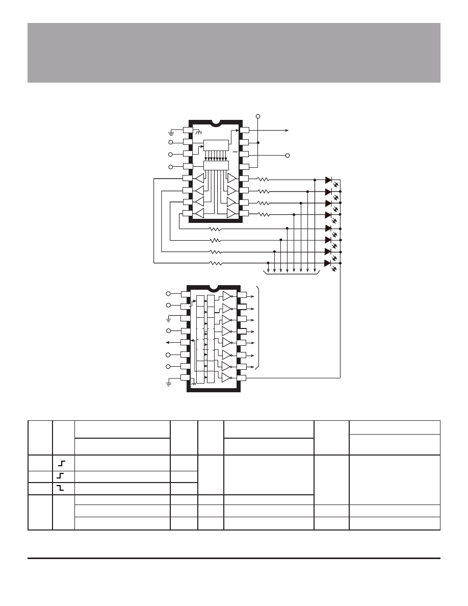
TYPICAL APPLICATION
TRUTH TABLE
Serial
Shift Register Contents
Serial
Latch Contents
Output Contents
Data
Clock
Data
Strobe
Output
Input
Input I
1
I
2
I
3
...
I
N-1
I
N
Output
Input
I
1
I
2
I
3
...
I
N-1
I
N
Enable
I
1
I
2
I
3
... I
N-1
I
N
H
H
R
1
R
2
...
R
N-2
R
N-1
R
N-1
L
L
R
1
R
2
...
R
N-2
R
N-1
R
N-1
X
R
1
R
2
R
3
...
R
N-1
R
N
R
N
X
X
X
...
X
X
X
L
R
1
R
2
R
3
...
R
N-1
R
N
P
1
P
2
P
3
...
P
N-1
P
N
P
N
H
P
1
P
2
P
3
...
P
N-1
P
N
L
P
1
P
2
P
3
... P
N-1
P
N
X
X
X
...
X
X
H
L
L
L
... L
L
L = Low Logic Level H = High Logic Level X = Irrelevant P = Present State R = Previous State
Dwg. No. B-1541
OUTPUT
ENABLE
STROBE
DATA OUT
DATA IN
+ 12 V
CLOCK
TO OTHER SEGMENTS
9
TO
OTHER
DIGITS
V
DD
OE
V
BB
1
2
3
4
5
6
7
8
16
15
14
13
12
11
10
9
SHIFT
REGISTER
LATCHES
1
2
3
4
5
6
7
8
16
15
14
13
12
11
10
9
LA
TCHES
SHIFT
REGISTER
+ 12 V
DATA OUT
FOR > 8 SEGMENTS
PER DIGIT
OUTPUT ENABLE
(ACTIVE LOW)
CLOCK
DATA IN
STROBE
UCN5895A
UCN5821A
C
5895
8-BIT SERIAL-INPUT,
LATCHED DRIVERS
115 Northeast Cutoff, Box 15036
Worcester, Massachusetts 01615-0036 (508) 853-5000
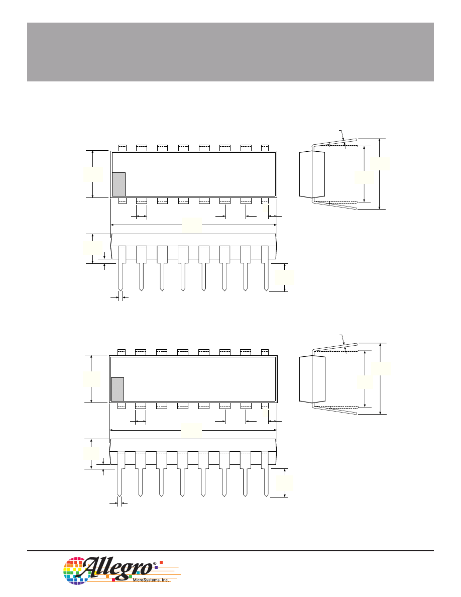
NOTES:
1. Lead thickness is measured at seating plane or below.
2. Lead spacing tolerance is non-cumulative.
3. Exact body and lead configuration at vendor’s option within limits shown.
0.014
0.008
0.300
BSC
Dwg. MA-001-16A in
0.430
MAX
16
1
8
0.280
0.240
0.210
MAX
0.070
0.045
0.015
MIN
0.022
0.014
0.100
BSC
0.005
MIN
0.150
0.115
9
0.775
0.735
0.355
0.204
7.62
BSC
Dwg. MA-001-16A mm
10.92
MAX
16
1
8
7.11
6.10
5.33
MAX
1.77
1.15
0.39
MIN
0.558
0.356
2.54
BSC
0.13
MIN
3.81
2.93
9
19.68
18.67
UCN5895A
Dimensions in Inches
(controlling dimensions)
Dimensions in Millimeters
(for reference only)
5895
8-BIT SERIAL-INPUT,
LATCHED DRIVERS
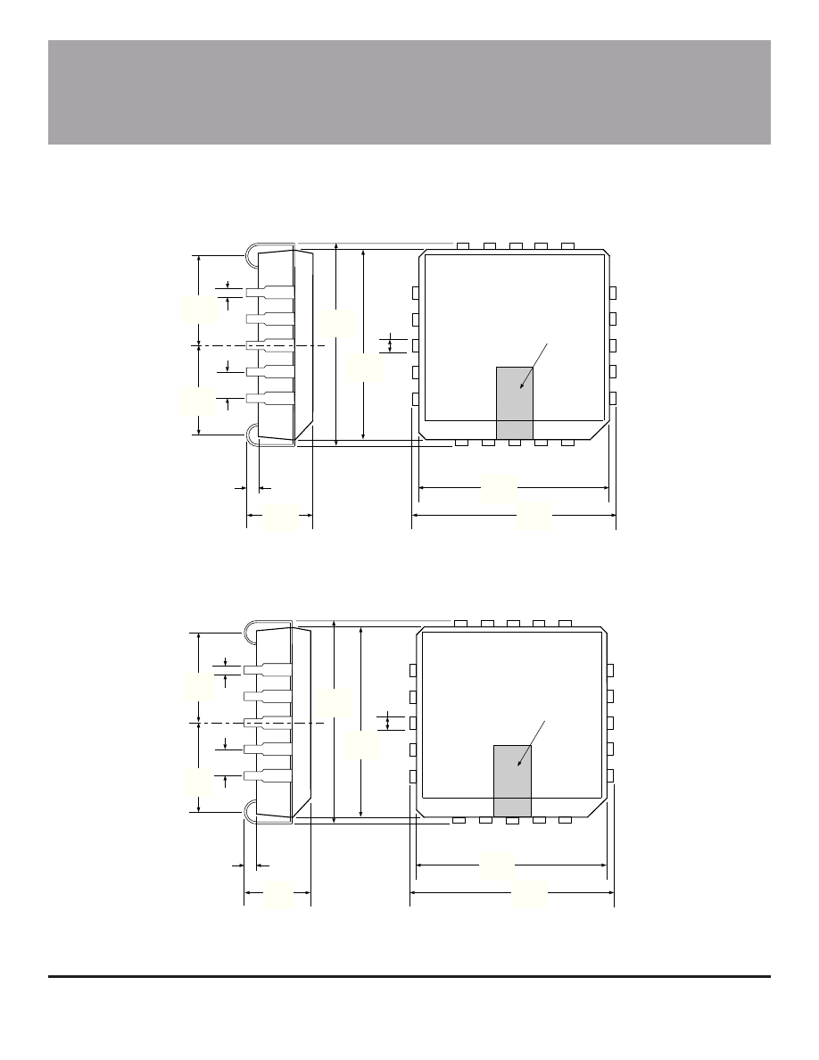
UCN5895EP
Dimensions in Inches
(controlling dimensions)
NOTES:
1. Lead spacing tolerance is non-cumulative.
2. Exact body and lead configuration at vendor’s option within limits shown.
9
13
0.51
MIN
4.57
4.20
1.27
BSC
1
20
2
Dwg. MA-005-20A mm
10.03
9.78
9.042
8.890
0.812
0.661
0.533
0.331
3
4
8
14
18
19
9.042
8.890
10.03
9.78
INDEX AREA
4.29
3.58
4.29
3.58
Dimensions in Millimeters
(for reference only)
9
13
0.020
MIN
0.180
0.165
0.050
BSC
1
20
2
Dwg. MA-005-20A in
0.395
0.385
0.356
0.350
0.032
0.026
0.021
0.013
3
4
8
14
18
19
0.356
0.350
0.395
0.385
INDEX AREA
0.169
0.141
0.169
0.141
5895
8-BIT SERIAL-INPUT,
LATCHED DRIVERS
115 Northeast Cutoff, Box 15036
Worcester, Massachusetts 01615-0036 (508) 853-5000
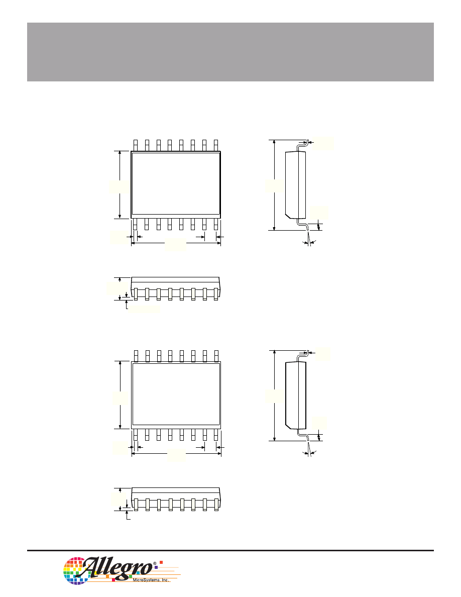
A5895SLW
Dimensions in Inches
(for reference only)
Dimensions in Millimeters
(controlling dimensions)
1
2
3
0.2992
0.2914
0.4133
0.3977
0.419
0.394
0.020
0.013
0.0926
0.1043
0.0040
MIN.
0.0125
0.0091
0.050
0.016
0
°
TO
8
°
Dwg. MA-008-16A in
0.050
BSC
16
9
9
16
1
2
3
7.60
7.40
10.50
10.10
10.65
10.00
0.51
0.33
2.65
2.35
0.10
MIN.
0.32
0.23
1.27
0.40
0
°
TO
8
°
Dwg. MA-008-16A mm
1.27
BSC
NOTES:
1. Lead spacing tolerance is non-cumulative.
2. Exact body and lead configuration at vendor’s option
within limits shown.
Allegro MicroSystems, Inc. reserves the right to make, from time to time,
such departures from the detail specifications as may be required to permit
improvements in the design of its products.
The information included herein is believed to be accurate and reliable.
However, Allegro MicroSystems, Inc. assumes no responsibility for its use; nor
for any infringements of patents or other rights of third parties which may result
from its use.
Wyszukiwarka
Podobne podstrony:
5895
5895
5895
5895
5895
5895
więcej podobnych podstron