TMC1175A
Video A/D Converter
8 bit, 40 Msps
www.fairchildsemi.com
REV. 1.3.3 2/28/02
Features
• 8-Bit resolution
• 40 Msps conversion rate
• Low power: 100mW at 20 Msps
• Integral track/hold
• Integral and differential linearity error 0.5 LSB
• Single or dual +5 Volt supplies
• Differential phase 0.5 degree
• Differential gain 1.5%
• Three-state TTL/CMOS-compatible outputs
• Low cost
Applications
• Video digitizing
• VGA and CCD digitizing
• LCD projection panels
• Image scanners
• Personal computer video boards
• Multimedia systems
• Low cost, high speed data conversion
Description
The TMC1175A analog-to-digital (A/D) converter employs
a two-step flash architecture to convert analog signals into
8-bit digital words at sample rates of up to 40 Msps
(Megasamples per second). An integral Track/Hold circuit
delivers excellent performance on signals with full-scale fre-
quency components up to 12 MHz. Innovative architecture
and submicron CMOS technology limit typical power dissi-
pation to 100 mW.
Power may be derived from either single or dual +5V
supplies. Internal voltage reference resistors allow self-bias
operation. Input capacitance is very low, simplifying or
eliminating input driving amplifiers. All digital three-state
outputs are TTL- and CMOS-compatible.
The TMC1175A is available in 24-lead plastic SOIC, and
28-lead J-lead PLCC packages. Performance specifications
are guaranteed from -20°C to 75°C.
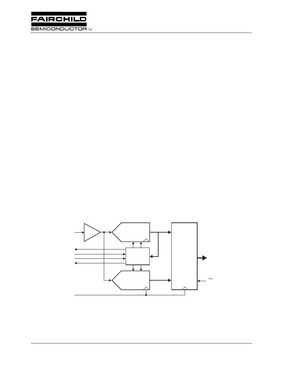
Block Diagram
Reference
Matrix
D
7-0
V
IN
VR+
R
T
R
B
VR–
Track/
Hold
OE
CONV
24453A
Coarse
Quantizer
Digital
Error-
Corrector
Fine
Quantizer

TMC1175A
PRODUCT SPECIFICATION
2
REV. 1.3.3 2/28/02
Functional Description
The TMC1175A 8-bit A/D converter uses a two-step archi-
tecture to perform analog-to-digital conversion at rates up to
40 Msps. The input signal is held in an integral track/hold
stage during the conversion process. Operation is pipelined,
with one input sample taken and one output word provided
for each CONVert cycle.
The first step in the conversion process is a coarse 4-bit
quantization. This determines the range of the subsequent
fine 4-bit quantization step. To eliminate spurious codes, the
fine 4-bit A/D quantizer output is gray-coded and converted
to binary before it is combined with the coarse result to form
a complete 8-bit result.
Analog Input and Voltage References
The TMC1175A converts analog signals in the range R
B
to
R
T
into digital data. Input signals outside that range produce
“saturated” 00h or FFh output codes. The device will not be
damaged by signals within the range A
GND
to V
DDA
.
Input voltage range is very flexible and extends from the +5
Volt power supply to ground. Performance is specified over
the optimom 2 volt input range: 0.6V to 2.6V. However, the
part will function with a full-scale range from 1.0V to 5.0V.
A reduced input range may simplify analog signal condition-
ing circuitry, at the expense of additional noise sensitivity
and reduced differential linearity. Increasing the range can
improve differential linearity, but imposes a greater burden
on the input signal conditioning circuitry.
In many applications, external voltage reference sources are
connected to the R
T
and R
B
pins. R
B
can be grounded. Gain
and offset errors are directly related to the accuracy and sta-
bility of the applied reference voltages.
Two reference pull-up and pull-down resistors connected to
VR+ and VR– are provided internally for operation without
external voltage reference circuitry (Figure 1). The reference
voltages applied to R
T
and R
B
may be generated by connect-
ing VR+ to R
T
and VR- to R
B
. The power supply voltage is
divided by the on-chip resistors to bias the R
T
and R
B
points.
This sets-up the converter for operation in its nominal range
from 0.6V to 2.6V.
Figure 1. Reference Resistors
With V
DDA
at 5.0V, connecting VR+ to R
T
and grounding
R
B
will provide an input range from 0.0V to 2.27V, while
connecting R
T
to V
DDA
and R
B
to VR- produces a full scale
range of 3.85V referenced to V
DDA
. External resistors may
also be employed to provide arbitrary reference voltages, but
they will not match the temperature coefficient of the on-
chip resistors as well as R+ and R-, and will cause the con-
verter transfer function to vary with temperature.
With this implementation, errors in the power supply voltage
end up on the conversion data output.
Because a two-step conversion process is employed, it is
important that the references remain stable during the
ENTIRE conversion process (two clock cycles). The refer-
ence voltage can then be changed, but any conversion in
progress during a reference change is invalid.
VDDA
VR+
R
T
R+
324
Ω
RREF
270
Ω
R–
81
Ω
R
B
VR–
+2.6V
+0.6V
27010A
PRODUCT SPECIFICATION
TMC1175A
REV. 1.3.3 2/28/02
3
Table 1. Output Coding
Note:
1. LSB = (R
T
– R
B
) / 255
Digital Inputs and Outputs
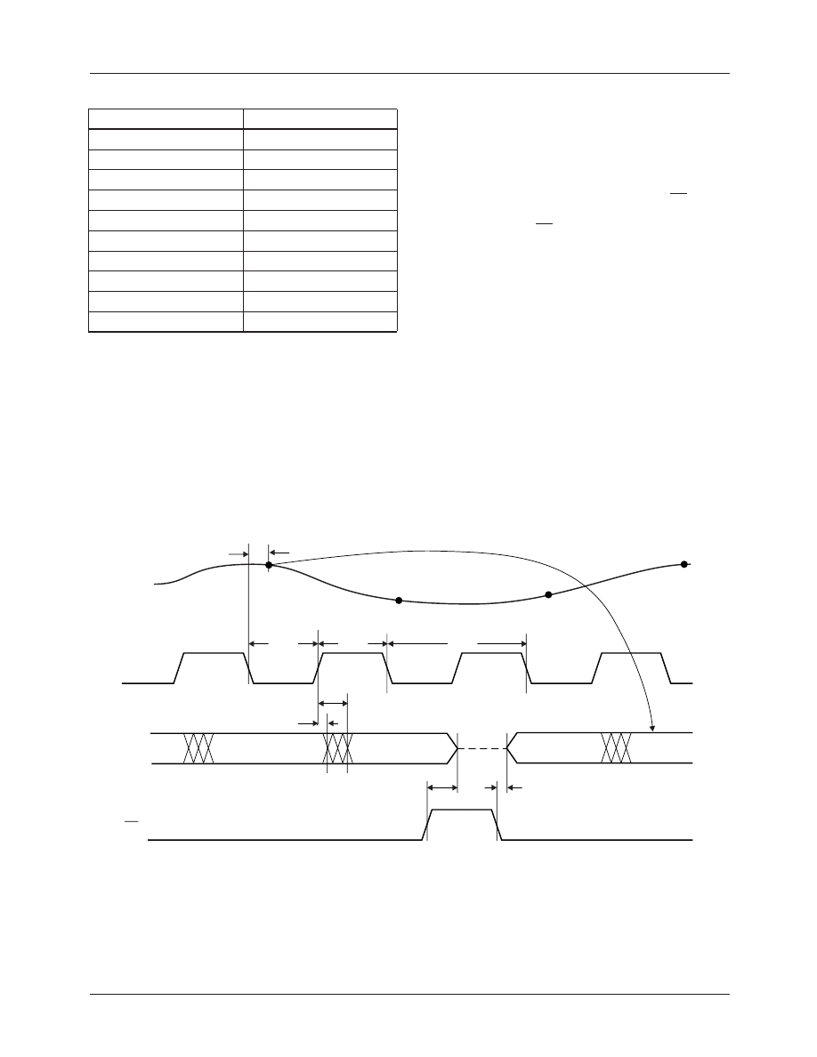
Sampling of the applied input signal takes place on the fall-
ing edge of the CONV signal (Figure 2). The output word is
delayed by 2 1/2 CONV cycles. It is then available after the
rising edge of CONV. The previous data on the output
Input Voltage
Output
R
T
+ 1 LSB
FF
R
T
FF
R
T
– 1 LSB
FE
• • •
• • •
R
B
+ 128 LSB
80
R
B
+ 127 LSB
7F
• • •
• • •
R
B
+ 1 LSB
01
R
B
00
R
B
– 1 LSB
00
remain valid for t
HO
(Output Hold Time), satisfying any
hold time requirement of the receiving circuit. The new data
become valid t
DO
(Output Delay Time) after this rising edge
of CONV.
The outputs of the TMC1175A are CMOS- and TTL-com-
patible, and are capable of driving four low-power Schottky
TTL (54/74LS) loads. An Output Enable control, OE, places
the outputs in a high-impedance state when HIGH. The out-
puts are enabled when OE is LOW.
Power and Ground
To minimize noise injection into the analog section, V
DDA
may be connected to a separate regulated +5 volt supply.
V
DDD
may be connected to a digital supply. Power up
sequence is immaterial. Latch-up will not occur.
A
GND
and D
GND
pins should be connected to a common
ground plane. For optimum performance treat analog and
digital PWB traces as transmission lines. Route analog
connections cleanly to the TMC1175A. Segregate digital
connections and if necessary terminate clocks to eliminate
ringing. Prevent digital returm currents from flowing across
analog input sections of the TMC1175A.
Figure 2. Conversion Timing
CONV
D
7-0
ORP
ORN
OE
V
IN
24455A
Data N–3
Data N–2
Data N–1
Data N
t
STO
t
PWL
t
HO
t
DIS
t
ENA
t
DO
t
PWH
1/f
S
Hi-Z
Sample N
Sample N+1
Sample N+2
Sample N+3
TMC1175A
PRODUCT SPECIFICATION
4
REV. 1.3.3 2/28/02
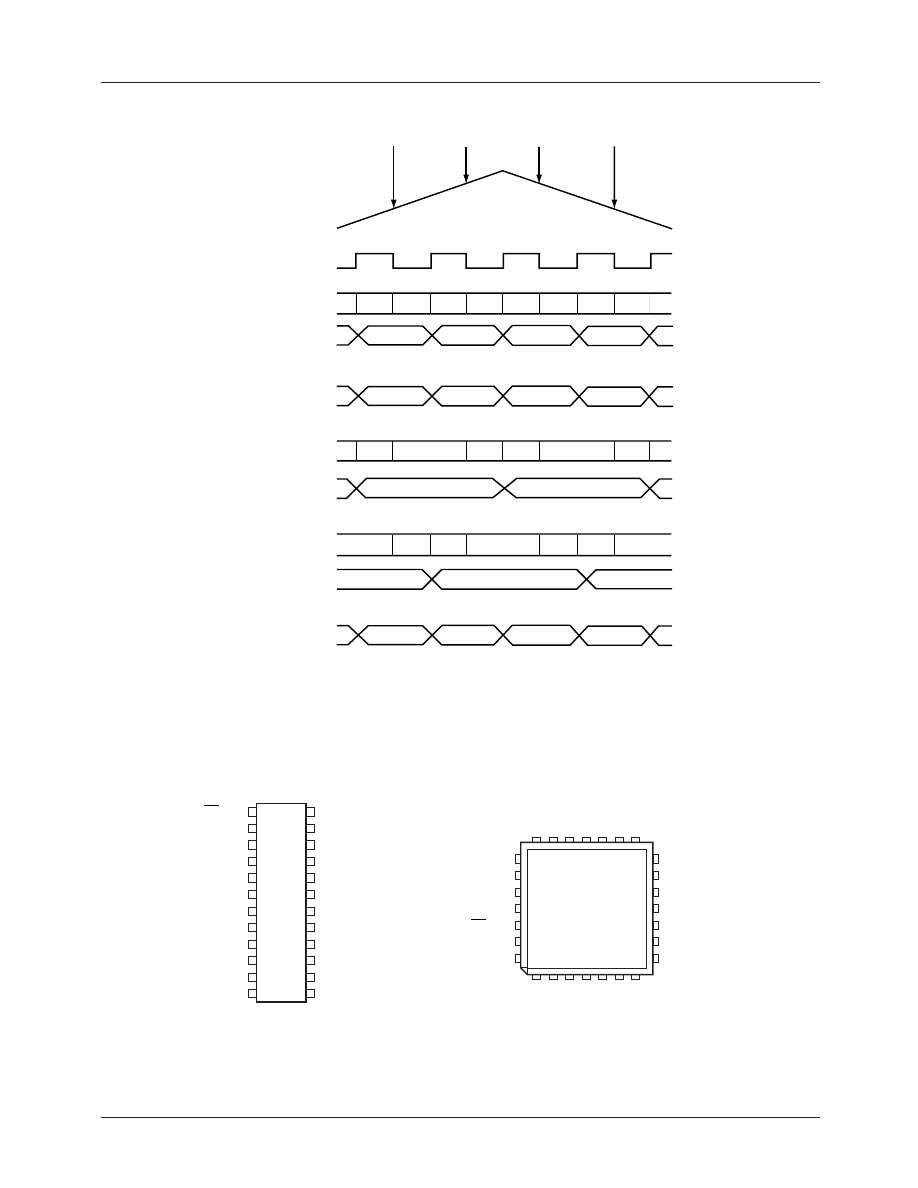
Analog input
External Clock
Upper comparators block
Lower comparators A block
Upper data
Lower reference voltage
Lower data A
Lower comparators B block
Lower data B
Digital output
S (1)
S (1)
H (1)
C (1)
S (2)
C (2)
C (3)
H (3)
C (3)
S (3)
S (3)
S (4)
C (4)
C (1)
MD (0)
MD (1)
MD (2)
MD (3)
RV (0)
RV (1)
RV (2)
RV (3)
LD (-1)
LD (1)
LD(-2)
LD(0)
LD(2)
Out(-2)
Out(-1)
Out(0)
Out(1)
V(1)
V(2)
V(3)
V(4)
H (0)
C (0)
S (2)
H (2)
C (2)
S (4)
H (94)
65-7568
Figure 3. Internal Timing
Pin Assignments
27
R
B
1
2
3
4
5
6
7
8
9
10
11
12
24
23
22
21
20
19
18
17
16
15
14
13
M7 Package
24454A
N/C
D
7
V
DDD
V
DDD
R3 Package
D1
D2
D3
N/C
N/C
D4
D5
D6
CONV
A
GND
A
GND
V
IN
V
DDA
R
T
VR+
V
DDA
V
DDA
1
N/C
26
2
3
28
4
5
6
7
8
9
10
11
12
24
25
23
22
21
20
19
18
17
16
15
14
13
VR–
D
GND
D
GND
D
GND
R
B
VR–
A
GND
A
GND
V
IN
V
DDA
R
T
VR+
V
DDA
V
DDA
V
DDD
OE
OE
D
GND
D
0
D
0
D
1
D
2
D
3
D
4
D
5
D
6
D
7
V
DDD
CONV

PRODUCT SPECIFICATION
TMC1175A
REV. 1.3.3 2/28/02
5
Pin Descriptions
Pin Name
Pin Number
Pin Type Pin Function Description
M7
R3
Inputs
V
IN
19
23
R
T
– R
B
Analog Input. The input voltage conversion range lies between the
voltages applied to the RT and RB pins.
R
T
17
20
2.6V
Reference Voltage Top Input. R
T
is the top input to the reference
resistor ladder. A DC voltage applied to R
T
defines the positive end
of the V
IN
conversion range.
R
B
23
27
0.6V
Reference Voltage Bottom Input. R
B
is the bottom input to the
reference resistor ladder. A DC voltage applied to R
B
defines the
negative end of the V
IN
conversion range.
VR+
16
19
Reference Voltage Top Source. VR+ is the internal pull-up
reference resistor for self-bias operations.
VR–
22
26
Reference Voltage Bottom Source. VR- is the internal pull-down
reference resistor for self-bias operations.
OE
1
2
CMOS
Output Enable. (CMOS-compatible) When LOW, D
7-0
are enabled.
When HIGH, D
7-0
are in a high-impedance state.
CONV
12
14
CMOS
Convert (Clock) Input. (CMOS-compatible) V
IN
is sampled on the
falling edge of CONV.
Outputs
D
7-0
10–3
12–9,
7–4
CMOS/
TTL
Data Outputs (D7 = MSB). Eight-bit CMOS- and TTL-compatible
digital outputs. Data is output following the rising edge of CONV.
Power
V
DDA
14, 15, 18
17, 18,
21
+5V
Analog Supply Voltage. Independent +5 volt power connection to
analog comparator circuits.
V
DDD
11, 13
13, 16
+5V
Digital Supply Voltage. Independent +5 volt power connection to
digital error correction and output drivers.
A
GND
20, 21
24, 25
0.0V
Analog Ground. Connect to the system analog ground plane.
D
GND
2, 24
3, 28
0.0V
Digital Ground. Connect to the system analog ground plane.
No Connect
N/C
1, 8, 15,
22
open
Not Connected.
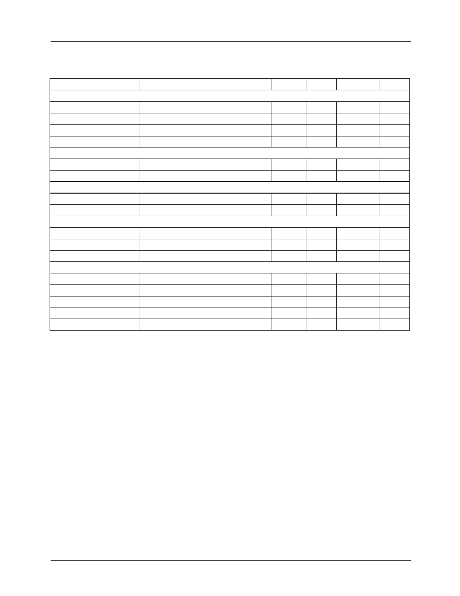
Bandwidth Specification Notes
The specification for bandwidth of an A/D converter is some-
what different from the normal frequency-response specifi-
cation used in amplifiers and filters. An understanding of the
differences will help in selecting converters properly for par-
ticular applications.
A/D conversion comprises two distinct processes: sampling
and quantizing. Sampling is “grabbing” a snapshot of the
input signal and holding it steady for quantizing. The quan-
tizing process is approximating the analog input, which may
be any value within the conversion range, with its nearest
numerical value. While sampling is a high-frequency pro-
cess, quantizing operates on a dc signal, held steady by the
track/hold circuit. Therefore, the sampling process is what
relates to the dynamic characteristics of the converter.
Sampling involves an aperture time, the time during which
the track/hold is trying to capture the input signal and settle
on a dc value to hold. It is analogous to the shutter speed of a
camera: the shorter the aperture (or faster the shutter) the less
the signal will be blurred, and the less uncertainty there will
be in the quantized value.
For example, a 10 MHz sinewave with a 1V peak amplitude
(2Vp-p) has a maximum slew rate of 2
πfA at zero crossing,
or 62.8V/µs. With an 8-bit A/D converter, q (the quantization
step size) = 2V/255 = 7.8mV. The input signal will slew one
LSB in 124ps. To limit the error (and noise) contribution due
to aperture effects to 1/2LSB, the aperture must be shorter
than 62ps.
TMC1175A
PRODUCT SPECIFICATION
6
REV. 1.3.3 2/28/02
This is the primary reason that the signal to noise ratio drops
off as full scale frequency increases. Note, also, that the slew
rate is directly proportional to signal amplitude, A. A/Ds will
handle lower-amplitude signals of higher bandwidth.
All this is of particular interest in applications such as digi-
tizing analog VGA RGB signals, or the output of a CCD
imaging chip. These data are effectively pre-sampled: there
is a period of rapid slewing from one pixel value to another,
followed by a relatively stable dc level before the signal
slews to the next pixel value. The goal is, of course, to
sample on these pixel values, not on the slewing between
pixels. During the aperture time, the A/D sees essentially a
dc signal, and classic bandwidth considerations are not
important. As long as the input circuit can slew and settle to
the new value in the prescribed period, an accurate conver-
sion will be made.
The TMC1175A is capable of slewing a full 2V and settling
between samples taken as little as 25ns apart, making it ideal
for digitizing analog VGA and CCD outputs.
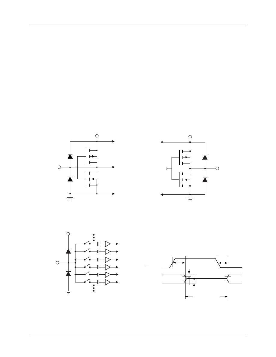
Equivalent Circuits and Threshold Level
Figure 4. Equivalent Digital Input Circuit
Figure 5. Equivalent Digital Output Circuit
Data or
Control
Input
V
DD
p
n
27014B
GND
V
DD
p
n
27011B
GND
Output
Figure 7. Threshold Levels for Three-State Measurements
65-1175A-07
t
ENA
2.0V
0.8V
t
DIS
Three-State
Outputs
OE
High Impedance
0.5V
0.5V
Figure 6. Equivalent Analog Input Circuit
V
DDA
A
GND
V
IN
27052A
PRODUCT SPECIFICATION
TMC1175A
REV. 1.3.3 2/28/02
7
Absolute Maximum Ratings
(beyond which the device may be damaged)
1
Notes:
1. Functional operation under any of these conditions is NOT implied. Performance and reliability are guaranteed only if
operating conditions are not exceeded.
2. Applied voltage must be current limited to specified range.
3. Forcing voltage must be limited to specified range.
4. Current is specified as conventional current flowing into the device
Parameter
Conditions
Min
Typ
Max
Unit
Power Supply Voltages
V
DDA
Measured to A
GND
-0.5
7.0
V
V
DDD
Measured to D
GND
-0.5
7.0
V
DDA
Measured to V
DDD
-0.5
0.5
V
A
GND
Measured to D
GND
-0.5
0.5
Digital Inputs
Applied Voltage
2
Measured to D
GND
-0.5
V
DDD
+ 0.5
V
Forced Current
3,4
-10.0
10.0
mA
Analog Inputs
Applied Voltage
2
Measured to A
GND
-0.5
V
DDA
+ 0.5
V
Forced Current
3,4
-10.0
10.0
mA
Outputs
Applied Voltage
2
Measured to D
GND
-0.5
V
DDD
+ 0.5
V
Forced Current
3,4
-6.0
6.0
mA
Short Circuit Duration
Single output in HIGH state to ground
1
sec
Temperature
Operating, Ambient
-20
110
°C
Junction
150
°C
Storage
-65
150
°C
Lead Soldering
10 seconds
300
°C
Vapor Phase Soldering
1 minute
220
°C
TMC1175A
PRODUCT SPECIFICATION
8
REV. 1.3.3 2/28/02
.
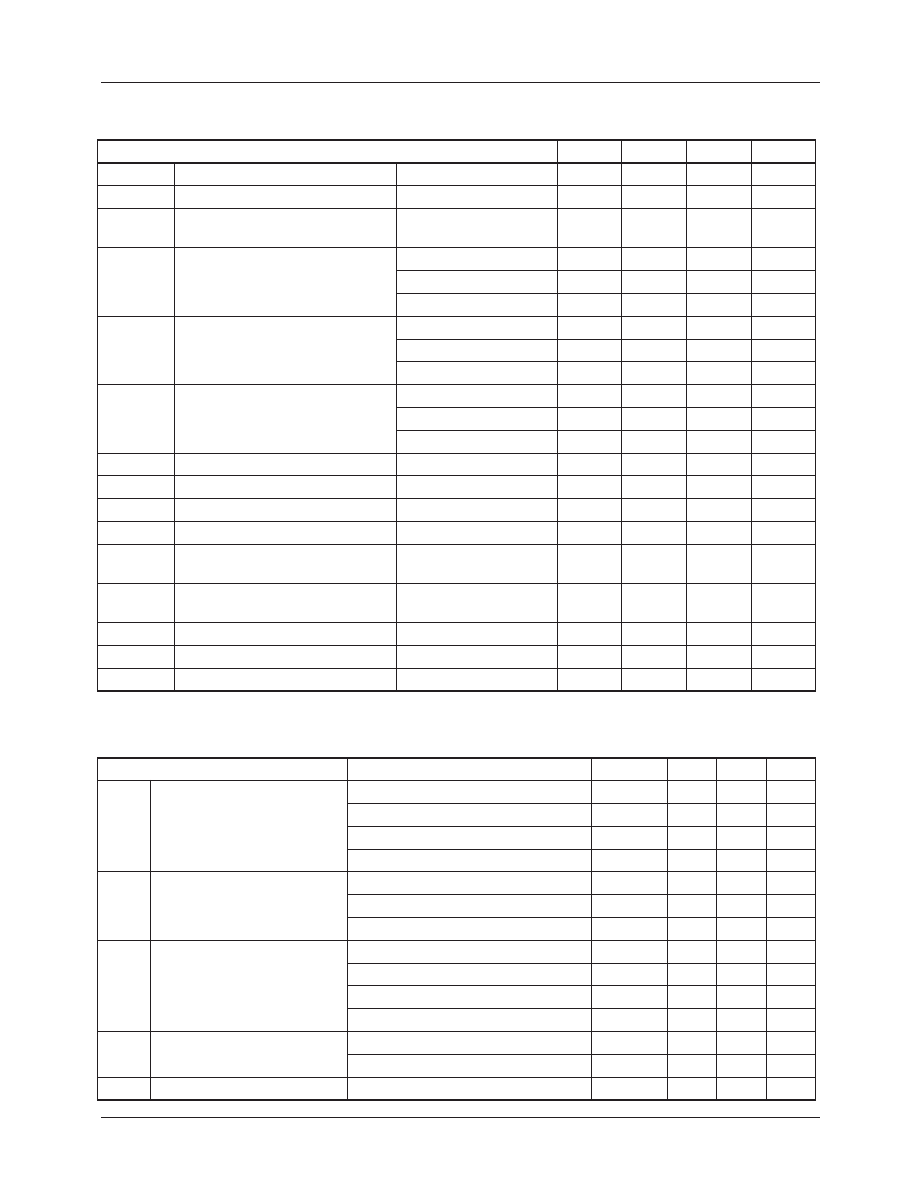
Operating Conditions
Parameter
Min
Nom
Max
Units
V
DDD
Digital Power Supply Voltage
4.75
5.0
5.25
V
V
DDA
Analog Power Supply Voltage
4.75
5.0
5.25
V
A
GND
Analog Ground (Measured to
D
GND
)
-0.1
0
0.1
V
f
S
Conversion Rate
TMC1175A-20
20
Msps
TMC1175A-30
30
Msps
TMC1175A-40
40
Msps
t
PWH
CONV Pulsewidth, HIGH
TMC1175A-20
15
ns
TMC1175A-30
13
ns
TMC1175A-40
12
ns
t
PWL
CONV Pulsewidth, LOW
TMC1175A-20
15
ns
TMC1175A-30
12
ns
TMC1175A-40
12
ns
V
RT
Reference Voltage, Top
2.0
2.6
V
DDA
V
V
RB
Reference Voltage, Bottom
0
0.6
3.0
V
V
RT-
V
RB
Reference Voltage Differential
1.0
5.0
V
V
IN
Analog Input Range
V
RB
V
RT
V
V
IH
Input Voltage, Logic HIGH
0.7 x
V
DDD
V
DDD
V
V
IL
Input Voltage, Logic LOW
GND
0.3 x
V
DDD
V
I
OH
Output Current, Logic HIGH
-4.0
mA
I
OL
Output Current, Logic LOW
4.0
mA
T
A
Ambient Temperature, Still Air
-20
75
°C
Electrical Characteristics
Parameter
Conditions
Min
Typ
1
Max
Units
I
DD
Power Supply Current
1
V
DDD
= V
DDA
= Max, C
LOAD
= 35pF
f
S
= 20Msps
20
30
mA
f
S
= 30Msps
25
35
mA
f
S
= 40Msps
30
40
mA
I
DDQ
Power Supply Current,
Quiescent
V
DDD
= V
DDA
= Max
CONV = LOW
7
18
mA
CONV = HIGH
10
20
mA
P
D
Total Power Dissipation
V
DDD
= V
DDA
= Max, C
LOAD
= 35pF
f
S
= 20Msps
100
160
mW
f
S
= 30Msps
125
185
mW
f
S
= 40Msps
150
210
mW
C
AI
Input Capacitance, Analog
CONV = LOW
4
pF
CONV = HIGH
12
pF
R
IN
Input Resistance
500
1000
k
Ω
PRODUCT SPECIFICATION
TMC1175A
REV. 1.3.3 2/28/02
9
Note:
1. Typical values with V
DDD
= V
DDA
= Nom and T
A
= Nom, Minimum/Maximum values with V
DDD
= V
DDA
= Max and T
A
= Min.
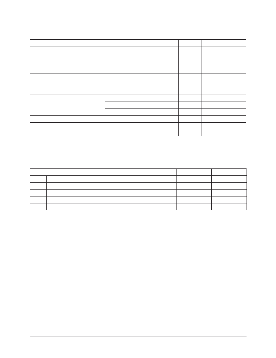
Switching Characteristics
I
CB
Input Current, Analog
±1
µA
R
REF
Reference Resistance
200
270
340
Ω
I
IH
Input Current, HIGH
V
DDD
= Max, V
IN
= V
DDD
±5
µA
I
IL
Input Current, LOW
V
DDD
= Max, V
IN
= 0V
±5
µA
I
OZH
Hi-Z Output Leakage
V
DDD
= Max, V
IN
= V
DDD
±5
µA
I
OZL
Hi-Z Output Leakage
V
DDD
= Max, V
IN
= 0V
±5
µA
I
OS
Short-Circuit Current
-30
mA
V
OH
Output Voltage, HIGH
I
OH
= -100µA
V
DDD
-0.3
V
I
OH
= -2.5mA
3.5
V
I
OH
= Max
2.4
V
V
OL
Output Voltage, LOW
I
OL
= Max
0.4
V
C
DI
Digital Input Capacitance
4
10
pF
C
DO
Digital Output Capacitance
10
pF
Parameter
Conditions
Min
Typ
Max
Units
t
STO
Sampling Time Offset
2
5
8
ns
t
HO
Output Hold Time
C
LOAD
= 15pF
5
ns
t
DO
Output Delay Time
C
LOAD
= 15pF
20
ns
t
ENA
Output Enable Time
27
ns
t
DIS
Output Disable Time
42
ns
Electrical Characteristics
(continued)
Parameter
Conditions
Min
Typ
1
Max
Units

TMC1175A
PRODUCT SPECIFICATION
10
REV. 1.3.3 2/28/02
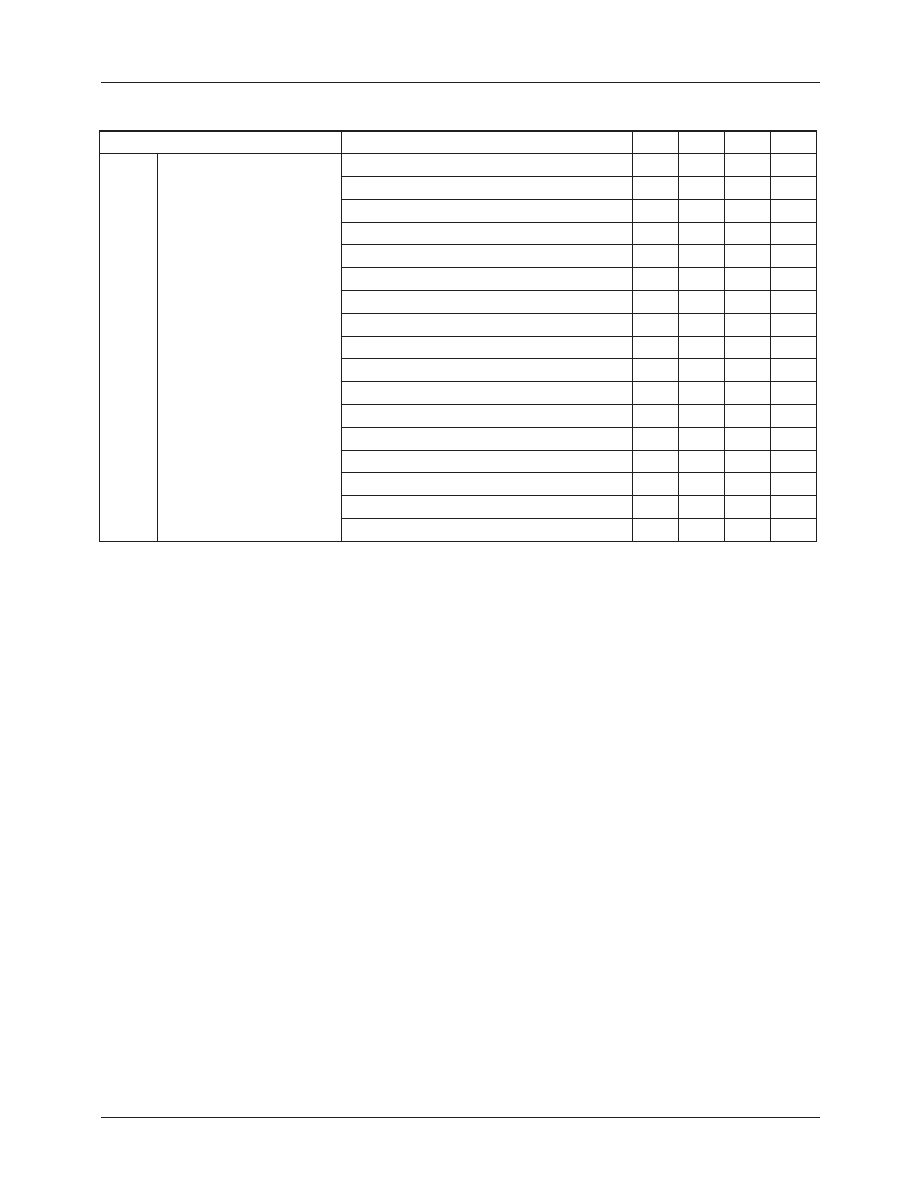
System Performance Characteristics
Parameter
Conditions
Min
Typ
1
Max
Units
E
LI
Integral Linearity Error,
Independent
V
RT
= 2.6V
V
RB
= 0.6V
±0.5
±1
LSB
E
LD
Differential Linearity Error
V
RT
= 2.6V
V
RB
= 0.6V
±0.3
±1
LSB
BW
Bandwidth
2
TMC1175A-20
TMC1175A-30
TMC1175A-40
10
12
12
MHz
MHz
MHz
E
AP
Aperture Error
30
ps
E
OT
Offset Voltage, Top
R
T
– V
IN
for most positive code transition
-8
-25
-42
mV
E
OB
Offset Voltage, Bottom
R
B
– V
IN
for most negative code transition
30
40
60
mV
dg
Differential Gain
f
S
= 14.3Msps
NTSC 40 IRE Mod Ramp
V
DDA
= +5.0V, T
A
=25°C
V
RT
= 2.6V, V
RB
= 0.6V
1.5
2.7
%
dp
Differential Phase
f
S
= 14.3Msps
NTSC 40 IRE Mod Ramp
V
DDA
= +5.0V, T
A
=25°C
V
RT
= 2.6V, V
RB
= 0.6V
0.5
1.0
deg
SNR
3
Signal-to-Noise Ratio
f
S
= 20Msps, V
RT
= 2.6V, V
RB
= 0.6V
f
IN
= 1.24MHz
44
48
dB
f
IN
= 2.48MHz
43
47
dB
f
IN
= 6.98MHz
41
45
dB
f
IN
= 10.0MHz
37
42
dB
f
S
= 30Msps, V
RT
= 2.6V, V
RB
= 0.6V
f
IN
= 1.24MHz
42
47
dB
f
IN
= 2.48MHz
40
45
dB
f
IN
= 6.98MHz
38
43
dB
f
IN
= 10.0MHz
33
39
dB
f
IN
= 12.0MHz
30
37
dB
f
S
= 40Msps, V
RT
= 2.6V, V
RB
= 0.6V
f
IN
= 1.24MHz
40
45
dB
f
IN
= 2.48MHz
38
43
dB
f
IN
= 6.98MHz
36
41
dB
f
IN
= 10.0MHz
34
38
dB
f
IN
= 12.0MHz
32
36
dB
PRODUCT SPECIFICATION
TMC1175A
REV. 1.3.3 2/28/02
11
Notes:
1. Values shown in Typ column are typical for V
DDD
= V
DDA
= +5V and T
A
= 25°C.
2. Bandwidth is the frequency up to which a full-scale sinewave can be digitized without spurious codes.
3. SNR values do not include the harmonics of the fundamental frequency.
4. SFDR is the ratio in dB of fundamental amplitude to the harmonic with the highest amplitude.
SFDR
4
Spurious-Free Dynamic
Range
f
S
= 20Msps, V
RT
= 2.6V, V
RB
= 0.6V
f
IN
= 1.24MHz
46
52
dB
f
IN
= 2.48MHz
44
51
dB
f
IN
= 6.98MHz
41
45
dB
f
IN
= 10.0MHz
38
43
dB
f
S
= 30Msps, V
RT
= 2.6V, V
RB
= 0.6V
f
IN
= 1.24MHz
42
49
dB
f
IN
= 2.48MHz
40
45
dB
f
IN
= 6.98MHz
37
41
dB
f
IN
= 10.0MHz
35
40
dB
f
IN
= 12.0MHz
34
39
dB
f
S
= 40Msps, V
RT
= 2.6V, V
RB
= 0.6V
f
IN
= 1.24MHz
40
44
dB
f
IN
= 2.48MHz
39
43
dB
f
IN
= 6.98MHz
38
41
dB
f
IN
= 10.0MHz
36
40
dB
f
IN
= 12.0MHz
36
39
dB
System Performance Characteristics
(continued)
Parameter
Conditions
Min
Typ
1
Max
Units
TMC1175A
PRODUCT SPECIFICATION
12
REV. 1.3.3 2/28/02
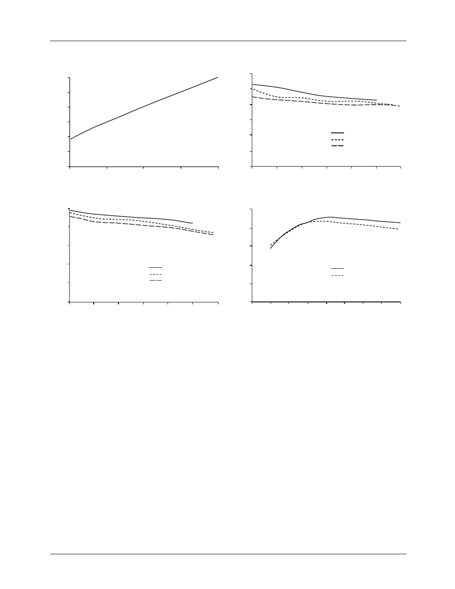
Typical Performance Characteristics
30
25
15
10
I DD
(mA)
5
0
0
10
20
30
40
20
60
50
30
20
SFDR
10
fs = 20 Msps
fs = 30 Msps
fs = 40 Msps
0
0
2
4
6
8
10
12
40
fs = 20 Msps
fs = 30 Msps
fs = 40 Msps
50
40
20
SNR
10
0
0
2
4
6
8
10
12
30
50
30
20
SNR
10
fs = 20 Msps
fs = 33 Msps
0
0
0.5
1.0
1.5
2.0
2.5
3.0
3.5
4.0
40
Figure 8. Typical I
DD
vs f
S
Figure 9. Typical SFDR vs f
IN
and f
S
Figure 10. Typical SNR vs f
IN
and f
S
Figure 11. Typical SNR vs Full Scale Input Range
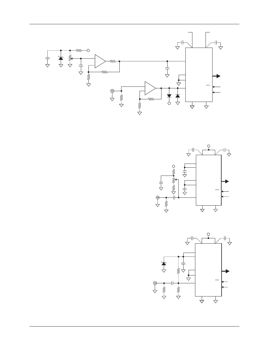
Applications Discussion
The circuit in Figure 12 employs a band-gap reference to
generate a variable RT reference voltages for the
TMC1175A as well as a bias voltage to offset the wideband
input amplifier to mid-range. An "offset adjust"
is also shown for varying the mid-range voltage level.
The operational amplifier in the reference circuitry is a
standard 741-type.
The voltage reference at R
T
can be adjusted from 0.0 to 2.4
volts while R
B
is grounded. Diodes are used to restrict the
wideband amplifier output to between -0.7V and V
DD
+0.7V. Diode protection is good practice to limit the analog
input voltage at V
IN
to the safe operating range.
The circuit in Figure 13 shows self-bias of R
T
and R
B
by
connection to VR+ and VR-. This sets up a 0.6 to 2.6 Volt
input range for V
IN
. The input range is susceptible to power
supply variation since the voltages on R
T
and R
B
are directly
derived from V
DDA
. The video input is AC-coupled and
biased at a adjustable midpoint of the A/D input range.
This circuit offers the advantage of minimum support
circuitry for the most cost-sensitive applications.
In Figure 14, an external band-gap reference sets R
T
to +1.2
Volts while R
B
is grounded. The internal pull-up resistor,
R+, provides the bias current for the band-gap reference. The
A/D converter input is biased to the mid-point of the input
range.
PRODUCT SPECIFICATION
TMC1175A
REV. 1.3.3 2/28/02
13
Figure 12. Typical Interface Circuit-High Performance
+5V
+
-
+
-
0.1
µF
2V
0.1mF
0.1
µF
VDDA
VDDD
VR+
RT
RB
VR-
VIN
AGND
DGND
OE
CONV
D7-0
TMC1175A
0.1
µF
0.1
µF
2k
Ω
1k
Ω
LM385
1k
Ω
1k
Ω
75
Ω
455
Ω
455
Ω
20
Ω
Video
Input
+5V
Regulated +5V
Gain Adjust
+5V
27056A
Wideband
Op-amp
Figure 13. Typical Interface Circuit – Low Cost
Figure 14. Typical Interface Circuit – Stabilized Reference
0.1
µF
0.1
µF
0.1
µF
10
µF
+5V
2.2k
Ω
2k
Ω
560
Ω
75
Ω
Video
Input
24458A
Offset
Adjust
+5V
0.1
µF
0.1
µF
VDDA
VDDD
VR+
RT
RB
VR-
VIN
AGND
DGND
OE
CONV
D7-0
TMC1175A
0.1
µF
10
µF
1k
Ω
1k
Ω
56
Ω
RF
Input
24457A
+5V
0.1
µF
0.1
µF
VDDA
VDDD
VR+
RT
RB
VR-
VIN
AGND
DGND
OE
CONV
D7-0
TMC1175A
LM385
Grounding
The TMC1175A has separate analog and digital
circuits. To keep digital system noise from the A/D
converter, it is recommended that power supply voltages
(V
DDD
and V
DDA
) originate from separate sources with
V
DDA
regulated, and that ground connections (D
GND
and
A
GND
) be made to the analog ground plane. Power supply
pins should be individually decoupled at the pin. The digital
circuitry that gets its input from the TMC1175A should be
referred to the system digital ground plane.
Printed Circuit Board Layout
Designing with high performance mixed-signal circuits
demands printed circuits with ground planes. Wire-wrap is
not an option, even for breadboarding. Overall system per-
formance is strongly influenced by the board layout. Capac-
itive coupling from digital to analog circuits may result in
poor A/D conversion. Consider the following suggestions
when doing the layout:
1.
Keep the critical analog traces (V
IN
, R
T
, R
B
, VR+,
VR-) as short as possible and as far as possible from all
digital signals. The TMC1175A should be located near
the board edge, close to the analog input connectors.
2.
The power plane for the TMC1175A should be sepa-
rate from that which supplies the rest of the digital cir-
cuitry. A single power plane should be used for all of
the V
DD
pins. If the power supply for the TMC1175A
is the same as that of the system's digital circuitry,
power to the TMC1175A should be decoupled with
ferrite beads and 0.1µF capacitors to reduce noise.
3.
The ground plane should be solid, not cross-hatched.
Connections to the ground plane should have very
short leads.

TMC1175A
PRODUCT SPECIFICATION
14
REV. 1.3.3 2/28/02
4.
Decoupling capacitors should be applied liberally to
V
DD
pins. Remember that not all power supply pins are
created equal. They supply different circuits on the inte-
grated circuit, each of which generate varying amounts
and types of noise. For best results, use 0.1µF ceramic
capacitors. Lead lengths should be minimized. Ceramic
chip capacitors are the best choice.
5.
If the digital power supply has a dedicated power plane
layer, it should not be placed under the TMC1175A, the
voltage reference, or the analog inputs. Capacitive cou-
pling of digital power supply noise from this layer to the
TMC1175A and its related analog circuitry can have an
adverse effect on performance.
6.
CONV should be handled carefully. Jitter and noise on
this clock may degrade performance. Terminate the
clock line at the CONV input, if required, to eliminate
overshoot and ringing.
Evaluation Board
An evaluation board is available that implements good inter-
face practices and provide a convenient testbed for develop-
ing system applications and circuit variations. An on-board
D/A converter is provided to reconstruct the digitized signal
and to evaluate converter performance.
Contact your sales representative for information.
PRODUCT SPECIFICATION
TMC1175A
REV. 1.3.3 2/28/02
15
Mechanical Dimensions
24 Lead SOIC (5.4 mm) Package
0.51
0.31
0.30
15.50
5.60
8.10
0.10
24
1.27 BSC
1.90
-
24
.050 BSC
.020
.004
.012
.012
.610
.220
.319
N
ccc
e
C
E
D
E1
A1
B
.014
.004
.006
.587
.205
.295
-
A
.067
.075
0.36
0.10
1.70
0.15
14.90
5.20
7.50
LEAD COPLANARITY
ccc
-C-
C
1
12
13
E
α
E1
h x 45
°
C
L
D
A
B
e
A1
24
SEATING PLANE
8
α°
0
8
0
0.50
1.27
h
L
.010
.016
.020
.050
0.25
0.41
Symbol
Inches
Min.
Max.
Min.
Max.
Millimeters
Notes
TMC1175A
PRODUCT SPECIFICATION
16
REV. 1.3.3 2/28/02
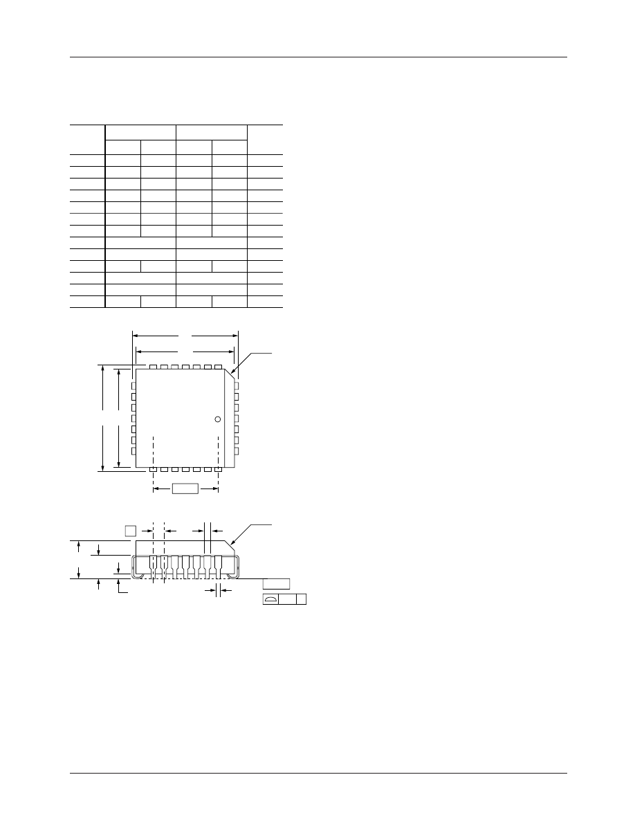
Mechanical Dimensions
(continued)
28 Lead PLCC Package
D
e
E
A
.165
.180
4.19
4.57
Symbol
Inches
Min.
Max.
Min.
Max.
Millimeters
Notes
E1
J
D1
A
A1
A2
B
B1
D3/E3
J
– C –
ccc C
LEAD COPLANARITY
A1
.090
.120
2.29
3.05
A2
.020
.51
—
—
B
.013
.021
.33
.53
D/E
.485
.495
12.32
12.57
D1/E1
.450
.456
11.43
11.58
D3/E3
.300 BSC
7.62 BSC
e
.050 BSC
1.27 BSC
J
.042
.048
1.07
1.22
2
3
ND/NE
7
7
N
28
28
ccc
.004
0.10
—
—
B1
.026
.032
.66
.81
Notes:
1.
2.
3.
All dimensions and tolerances conform to ANSI Y14.5M-1982
Corner and edge chamfer (J) = 45
°
Dimension D1 and E1 do not include mold protrusion. Allowable
protrusion is .101" (.25mm)
TMC1175A
PRODUCT SPECIFICATION
2/28/02 0.0m 002
Stock#DS7001175A
2002 Fairchild Semiconductor Corporation
DISCLAIMER
FAIRCHILD SEMICONDUCTOR RESERVES THE RIGHT TO MAKE CHANGES WITHOUT FURTHER NOTICE TO ANY
PRODUCTS HEREIN TO IMPROVE RELIABILITY, FUNCTION OR DESIGN. FAIRCHILD DOES NOT ASSUME ANY
LIABILITY ARISING OUT OF THE APPLICATION OR USE OF ANY PRODUCT OR CIRCUIT DESCRIBED HEREIN; NEITHER
DOES IT CONVEY ANY LICENSE UNDER ITS PATENT RIGHTS, NOR THE RIGHTS OF OTHERS.
LIFE SUPPORT POLICY
FAIRCHILD’S PRODUCTS ARE NOT AUTHORIZED FOR USE AS CRITICAL COMPONENTS IN LIFE SUPPORT DEVICES
OR SYSTEMS WITHOUT THE EXPRESS WRITTEN APPROVAL OF THE PRESIDENT OF FAIRCHILD SEMICONDUCTOR
CORPORATION. As used herein:
1. Life support devices or systems are devices or systems
which, (a) are intended for surgical implant into the body,
or (b) support or sustain life, or (c) whose failure to perform
when properly used in accordance with instructions for use
provided in the labeling, can be reasonably expected to
result in significant injury to the user.
2. A critical component is any component of a life support
device or system whose failure to perform can be
reasonably expected to cause the failure of the life support
device or system, or to affect its safety or effectiveness.
www.fairchildsemi.com
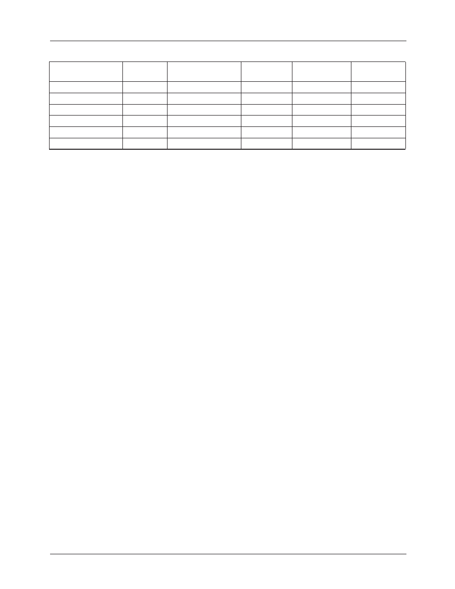
Ordering Information
Product Number
Conversion
Rate
Temperature Range
Screening
Package
Package
Marking
TMC1175AM7C20
20 Msps
T
A
= -20°C to 75°C Commercial
24-Lead
SOIC
1175AM7C20
TMC1175AM7C30
30 Msps
T
A
= -20°C to 75°C Commercial
24-Lead
SOIC
1175AM7C30
TMC1175AM7C40
40 Msps
T
A
= -20°C to 75°C Commercial
24-Lead
SOIC
1175AM7C40
TMC1175AR3C20
20 Msps
T
A
= -20°C to 75°C Commercial
28-Lead
PLCC
1175AR3C20
TMC1175AR3C30
30 Msps
T
A
= -20°C to 75°C Commercial
28-Lead
PLCC
1175AR3C30
TMC1175AR3C40
40 Msps
T
A
= -20°C to 75°C Commercial
28-Lead
PLCC
1175AR3C40
Wyszukiwarka
Podobne podstrony:
MPSA65, MMBTA65, PZTA65 (Fairchild Semiconductor)
H11A817 (Fairchild Semiconductor)
PN2222A, MMBT2222A, PZT2222A (Fairchild Semiconductor)
2N546x, MMBF546x (Fairchild Semiconductor)
BCV27 (Fairchild Semiconductor)
2N3906, MMBT3906, PZT3906 (Fairchild Semiconductor)
FOD3120 (Fairchild Semiconductor)
FQPF17N40 (Fairchild Semiconductor)
TIP100, TIP101, TIP102 (Fairchild Semiconductor)
MJE2955T (Fairchild Semiconductor)
PN2222 (Fairchild Semiconductor)
BC327, BC328 (Fairchild Semiconductor)
FOD817 (Fairchild Semiconductor)
KSP94 (Fairchild Semiconductor)
MOC8030, MOC8050 (Fairchild Semiconductor)
H22B1, H22B2, H22B3 (Fairchild Semiconductor)
więcej podobnych podstron