G
D
S
2N5460
2N5461
2N5462
MMBF5460
MMBF5461
MMBF5462
P-Channel General Purpose Amplifier
This device is designed primarily for low level audio and general
purpose applications with high impedance signal sources. Sourced
from Process 89.
Absolute Maximum Ratings*
TA = 25°C unless otherwise noted
*
These ratings are limiting values above which the serviceability of any semiconductor device may be impaired.
NOTES:
1) These ratings are based on a maximum junction temperature of 150 degrees C.
2) These are steady state limits. The factory should be consulted on applications involving pulsed or low duty cycle operations.
Thermal Characteristics
TA = 25°C unless otherwise noted
-
Symbol
Parameter
Value
Units
V
DG
Drain-Gate Voltage
- 40
V
V
GS
Gate-Source Voltage
40
V
I
GF
Forward Gate Current
10
mA
T
J
,T
stg
Operating and Storage Junction Temperature Range
-55 to +150
°
C
Symbol
Characteristic
Max
Units
2N5460-5462
*MMBF5460-5462
P
D
Total Device Dissipation
Derate above 25
°
C
350
2.8
225
1.8
mW
mW/
°
C
R
θ
JC
Thermal Resistance, Junction to Case
125
°
C/W
R
θ
JA
Thermal Resistance, Junction to Ambient
357
556
°
C/W
G
S
D
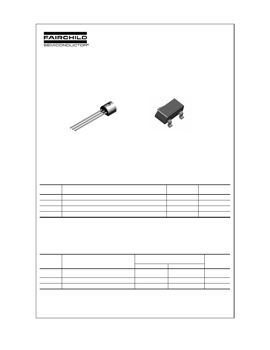
TO-92
SOT-23
Mark: 6E / 61U / 61V
*
Device mounted on FR-4 PCB 1.6" X 1.6" X 0.06."
2001 Fairchild Semiconductor Corporation
NOTE: Source & Drain
are interchangeable
2N5460 / 5461 / 5462 / MMBF5460 / MMBF5461 / MMBF5462
2N5460/5461/5462/MMBF5460/5461/5462, Rev A
5
Electrical Characteristics
TA = 25°C unless otherwise noted
OFF CHARACTERISTICS
Symbol
Parameter
Test Conditions
Min
Typ
Max Units
V
(BR)GSS
Gate-Source Breakdown Voltage
I
G
= 10
µ
A, V
DS
= 0
40
V
I
GSS
Gate Reverse Current
V
GS
= 20 V, V
DS
= 0
V
GS
= 20 V, V
DS
= 0, T
A
= 100
°
C
5.0
1.0
nA
µ
A
V
GS(off)
Gate-Source Cutoff Voltage
V
DS
= 15 V, I
D
= 1.0
µ
A
5460
5461
5462
0.75
1.0
1.8
6.0
7.5
9.0
V
V
V
V
GS
Gate-Source Voltage
V
DS
= 15 V, I
D
= 0.1 mA
5460
V
DS
= 15 V, I
D
= 0.2 mA
5461
V
DS
= 15 V, I
D
= 0.4 mA
5462
0.5
0.8
1.5
4.0
4.5
6.0
V
V
V
ON CHARACTERISTICS
I
DSS
Zero-Gate Voltage Drain Current*
V
DS
= 15 V, V
GS
= 0
5460
5461
5462
- 1.0
- 2.0
- 4.0
- 5.0
- 9.0
- 16
mA
mA
mA
SMALL SIGNAL CHARACTERISTICS
nV/
√
Hz
g
fs
Forward Transfer Conductance
V
DS
= 15 V, V
GS
= 0, f = 1.0 kHz
5460
5461
5462
1000
1500
2000
4000
5000
6000
µ
mhos
µ
mhos
µ
mhos
g
os
Output Conductance
V
DS
= 15 V, V
GS
= 0, f = 1.0 kHz
75
µ
mhos
C
iss
Input Capacitance
V
DS
= 15 V, V
GS
= 0, f = 1.0 MHz
5.0
7.0
pF
C
rss
Reverse Transfer Capacitance
V
DS
= 15 V, V
GS
= 0, f = 1.0 MHz
1.0
2.0
pF
NF
Noise Figure
V
DS
= 15 V, V
GS
= 0,
R
G
= 1.0 megohm, f = 100 Hz,
BW = 1.0 Hz
1.0
2.5
dB
e
n
Equivalent Short-Circuit Input
Noise Voltage
V
DS
= 15 V, V
GS
= 0, f = 100 Hz,
BW = 1.0 Hz
60
115
*
Pulse Test: Pulse Width
≤
300 ms, Duty Cycle
≤
2%
P-Channel General Purpose Amplifier
(continued)
2N5460 / 5461 / 5462 / MMBF5460 / MMBF5461 / MMBF5462
Typical Characteristics
(continued)
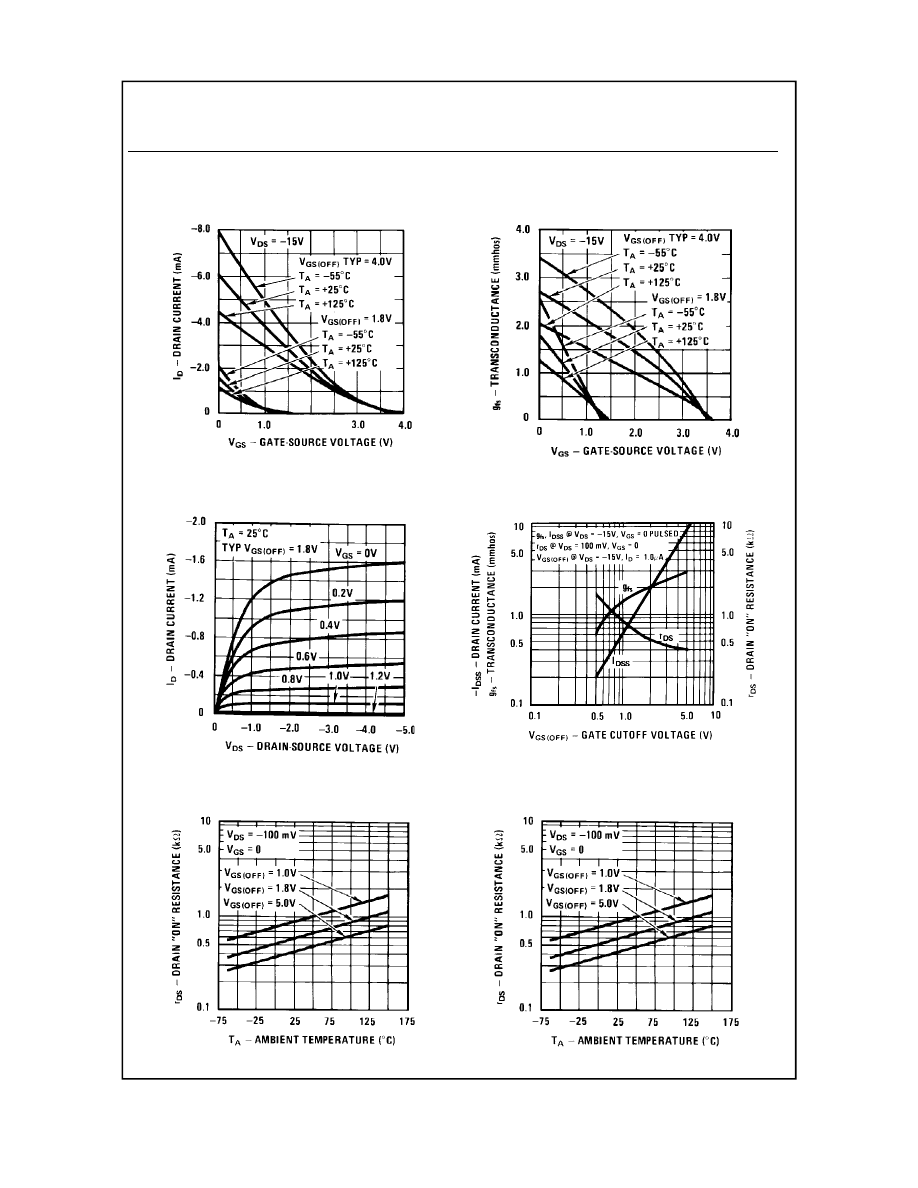
Channel Resistance vs.
Temperature
Leakage Current vs. Voltage
Transfer Charactersitics
Common Drain-Source
Transfer Characteristics
P-Channel General Purpose Amplifier
(continued)
Parameter Interactions
2N5460 / 5461 / 5462 / MMBF5460 / MMBF5461 / MMBF5462
5
Typical Characteristics
(continued)
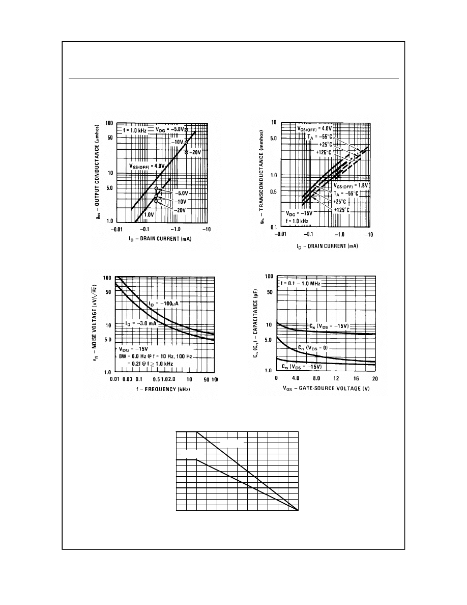
Noise Voltage vs. Frequency
Capacitance vs. Voltage
Output Conductance vs.
Drain Current
Transconductance vs.
Drain Current
Power Dissipation vs.
Ambient Temperature
0
25
50
75
100
125
150
0
50
100
150
200
250
300
350
TEMPERATURE ( C)
P - POWER DISSIPATION (mW)
º
D
SOT-23
TO-92
P-Channel General Purpose Amplifier
(continued)
2N5460 / 5461 / 5462 / MMBF5460 / MMBF5461 / MMBF5462

TRADEMARKS
The following are registered and unregistered trademarks Fairchild Semiconductor owns or is authorized to use and is
not intended to be an exhaustive list of all such trademarks.
LIFE SUPPORT POLICY
FAIRCHILD’S PRODUCTS ARE NOT AUTHORIZED FOR USE AS CRITICAL COMPONENTS IN LIFE SUPPORT
DEVICES OR SYSTEMS WITHOUT THE EXPRESS WRITTEN APPROVAL OF FAIRCHILD SEMICONDUCTOR CORPORATION.
As used herein:
1. Life support devices or systems are devices or
systems which, (a) are intended for surgical implant into
the body, or (b) support or sustain life, or (c) whose
failure to perform when properly used in accordance
with instructions for use provided in the labeling, can be
reasonably expected to result in significant injury to the
user.
2. A critical component is any component of a life
support device or system whose failure to perform can
be reasonably expected to cause the failure of the life
support device or system, or to affect its safety or
effectiveness.
PRODUCT STATUS DEFINITIONS
Definition of Terms
Datasheet Identification
Product Status
Definition
Advance Information
Preliminary
No Identification Needed
Obsolete
This datasheet contains the design specifications for
product development. Specifications may change in
any manner without notice.
This datasheet contains preliminary data, and
supplementary data will be published at a later date.
Fairchild Semiconductor reserves the right to make
changes at any time without notice in order to improve
design.
This datasheet contains final specifications. Fairchild
Semiconductor reserves the right to make changes at
any time without notice in order to improve design.
This datasheet contains specifications on a product
that has been discontinued by Fairchild semiconductor.
The datasheet is printed for reference information only.
Formative or
In Design
First Production
Full Production
Not In Production
DISCLAIMER
FAIRCHILD SEMICONDUCTOR RESERVES THE RIGHT TO MAKE CHANGES WITHOUT FURTHER
NOTICE TO ANY PRODUCTS HEREIN TO IMPROVE RELIABILITY, FUNCTION OR DESIGN. FAIRCHILD
DOES NOT ASSUME ANY LIABILITY ARISING OUT OF THE APPLICATION OR USE OF ANY PRODUCT
OR CIRCUIT DESCRIBED HEREIN; NEITHER DOES IT CONVEY ANY LICENSE UNDER ITS PATENT
RIGHTS, NOR THE RIGHTS OF OTHERS.
OPTOPLANAR™
PACMAN™
POP™
PowerTrench
QFET™
QS™
QT Optoelectronics™
Quiet Series™
SILENT SWITCHER
SMART START™
Stealth™
FAST
FASTr™
FRFET™
GlobalOptoisolator™
GTO™
HiSeC™
ISOPLANAR™
LittleFET™
MicroFET™
MICROWIRE™
OPTOLOGIC™
Rev. H2
ACEx™
Bottomless™
CoolFET™
CROSSVOLT™
DenseTrench™
DOME™
EcoSPARK™
E
2
CMOS
TM
EnSigna
TM
FACT™
FACT Quiet Series™
SuperSOT™-3
SuperSOT™-6
SuperSOT™-8
SyncFET™
TinyLogic™
UHC™
UltraFET
VCX™
Wyszukiwarka
Podobne podstrony:
2N545x, MMBF545x (Fairchild Semiconductor)
MPSA65, MMBTA65, PZTA65 (Fairchild Semiconductor)
H11A817 (Fairchild Semiconductor)
PN2222A, MMBT2222A, PZT2222A (Fairchild Semiconductor)
TMC1175 (Fairchild Semiconductor)
BCV27 (Fairchild Semiconductor)
2N3906, MMBT3906, PZT3906 (Fairchild Semiconductor)
FOD3120 (Fairchild Semiconductor)
FQPF17N40 (Fairchild Semiconductor)
TIP100, TIP101, TIP102 (Fairchild Semiconductor)
MJE2955T (Fairchild Semiconductor)
PN2222 (Fairchild Semiconductor)
BC327, BC328 (Fairchild Semiconductor)
FOD817 (Fairchild Semiconductor)
KSP94 (Fairchild Semiconductor)
MOC8030, MOC8050 (Fairchild Semiconductor)
więcej podobnych podstron