1999 May 17
1
Philips Semiconductors
Handling MOS devices
General
HANDLING MOS DEVICES
(1)
Electrostatic charges
Electrostatic charges can exist in many things; for
example, man-made-fibre clothing, moving machinery,
objects with air blowing across them, plastic storage bins,
sheets of paper stored in plastic envelopes, paper from
electrostatic copying machines, and people. The charges
are caused by friction between two surfaces, at least one
of which is non-conductive. The magnitude and polarity of
the charges depend on the different affinities for electrons
of the two materials rubbing together, the friction force and
the humidity of the surrounding air.
Electrostatic discharge is the transfer of an electrostatic
charge between bodies at different potentials and occurs
with direct contact or when induced by an electrostatic
field. Our devices can be damaged if the following
precautions are not taken.
Work station
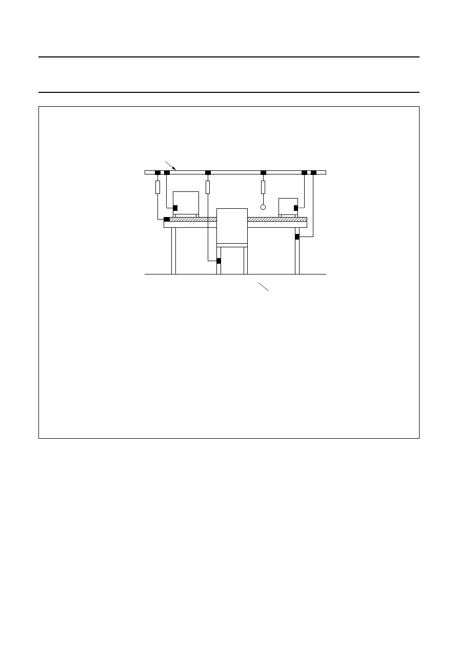
Figure 1 shows a working area suitable for safely handling
electrostatic sensitive devices. It has a work bench, the
surface of which is conductive or covered by an antistatic
sheet. Typical resistivity for the bench surface is between
1 and 500 k
Ω
per cm
2
. The floor should also be covered
with antistatic material.
The following precautions should be observed:
•
Persons at a work bench should be earthed via a wrist
strap and a resistor.
•
All mains-powered electrical equipment should be
connected via an earth leakage switch.
•
Equipment cases should be earthed.
•
Relative humidity should be maintained between 50 and
65%.
•
An ionizer should be used to neutralize objects with
immobile static charges.
Receipt and storage
Our devices are packed for dispatch in
antistatic/conductive containers, usually boxes, tubes or
blister tape. The fact that the contents are sensitive to
electrostatic discharge is shown by warning labels on both
primary and secondary packing.
(1)
These products are supplied in anti-static packing to
prevent damage caused by electrostatic discharge
during transport and handling. For further information,
refer to Philips specs.: SNW-EQ-608, SNW-FQ-302A
and SNW-FQ-302B.
The devices should be kept in their original packing whilst
in storage. If a bulk container is partially unpacked, the
unpacking should be performed at a protected work
station. Any devices that are stored temporarily should be
packed in conductive or antistatic packing or carriers.
Assembly
The devices must be removed from their protective
packing with earthed component pincers or short-circuit
clips. Short-circuit clips must remain in place during
mounting, soldering and cleansing/drying processes. Do
not remove more devices from the storage packing than
are needed at any one time. Production/assembly
documents should state that the product contains
electrostatic sensitive devices and that special precautions
need to be taken.
All tools used during assembly, including soldering tools
and solder baths, must be earthed. All hand tools should
be of conductive or antistatic material and, where possible,
should not be insulated.
Measuring and testing of completed circuit boards must be
done at a protected work station. Place the soldered side
of the circuit board on conductive or antistatic foam and
remove the short-circuit clips. Remove the circuit board
from the foam, holding the board only at the edges. Make
sure the circuit board does not touch the conductive
surface of the work bench. After testing, replace the circuit
board on the conductive foam to await packing.
Assembled circuit boards should be handled in the same
way as unmounted devices. They should also carry
warning labels and be packed in conductive or antistatic
packing.

1999 May 17
2
Philips Semiconductors
Handling MOS devices
General
,,,,,,,,,,
handbook, full pagewidth
(1)
(2)
(3)
(4)
(2)
(6)
(2)
(7)
(8)
MLB049
(5)
(9)
Fig.1 Protected work station.
(1) Earthing rail.
(2) Resistor (500 k
Ω ±
10%, 0.5 W).
(3) Ionizer.
(4) Work bench.
(5) Chair.
(6) Wrist strap.
(7) Electrical equipment.
(8) Conductive surface/antistatic sheet.
(9) Antistatic floor.
Wyszukiwarka
Podobne podstrony:
SC07 MARKING 1999 1
Ustawa z dnia 25 06 1999 r o świadcz pien z ubezp społ w razie choroby i macierz
brzuch 1999 2000
chojnicki 1999 20 problemy GP
Porty morskie i żegluga morska w Polsce w latach 1999 2001
ABS Octawia 1999
1999 05 05 0953
ED 1999 1 41
Badanie wahadła skrętnego, Studia, Pracownie, I pracownia, 7 Badanie drgań wahadła skrętnego {torsyj
Okręgi wojskowe od roku 1999, wiedza o siłach zbrojnych
MATHEMATICS HL May 1999 P1
1999 02 str 24 25 Chaotyczne rachunki
1999 12 22 2757
1999 06 Szkoła konstruktorów
0415191246 Routledge Humes Naturalism May 1999
PN EN 60099 5 1999 Ograniczniki przepięć Zasady doboru
897656 1300SRM0568 (10 1999) UK EN
więcej podobnych podstron