HCF4503
HEX BUFFER
February 2000
■
1 TTL-LOAD OUTPUT DRIVE CAPABILITY
■
2 OUTPUT-DISABLE CONTROLS
■
3 STATE OUTPUTS
■
5V, 10V, AND 15V PARAMETRIC RATINGS
■
QUIESCENT CURRENT SPECIFIED UP TO
15V
■
INPUT CURRENT OF 300nA AT 15V AND
25
°
C
■
100% TESTED FOR QUIESCENT CURRENT
MEETS
ALL
REQUIREMENTS
OF
JEDEC
TENTATIVE STANDARD N
0
. 13A, ”STANDARD
SPECIFICATIONS FOR DESCRIPTION OF ”B”
SERIES CMOS DEVICES”
DESCRIPTION
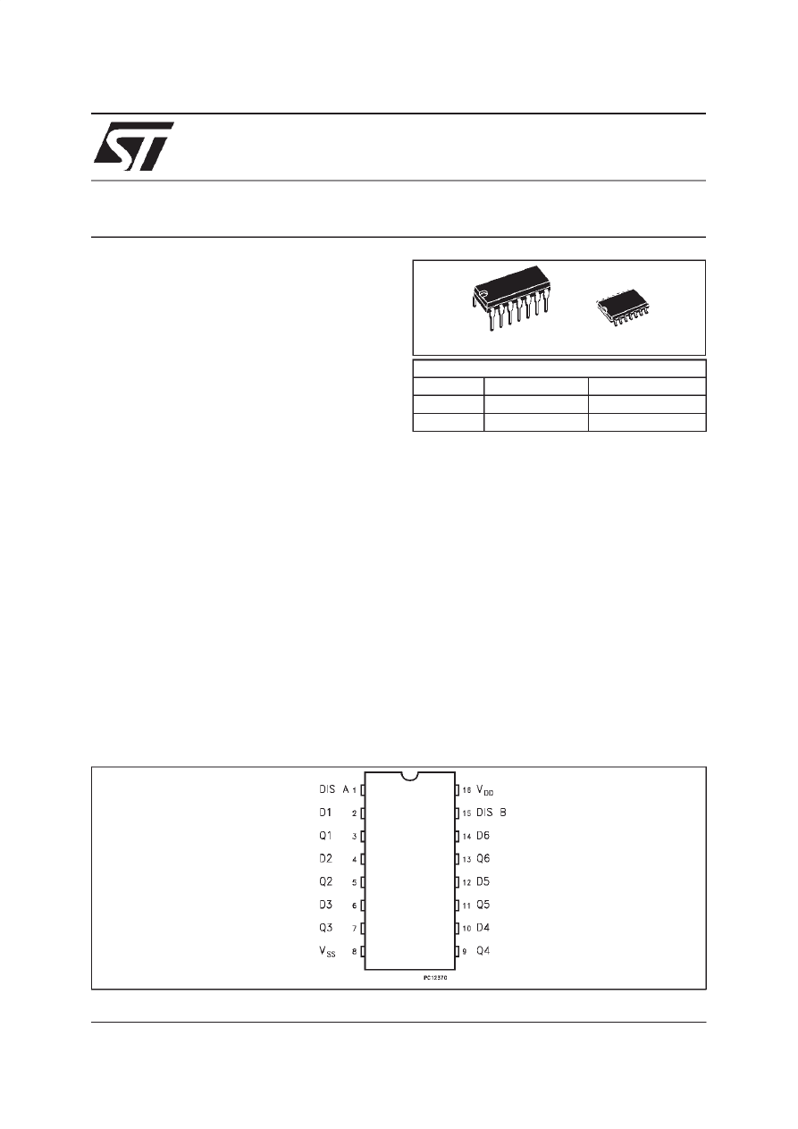
The HCF4503B is a monolithic integrated circuits,
available in 16-lead dual in-line plastic package
and plastic micro package.
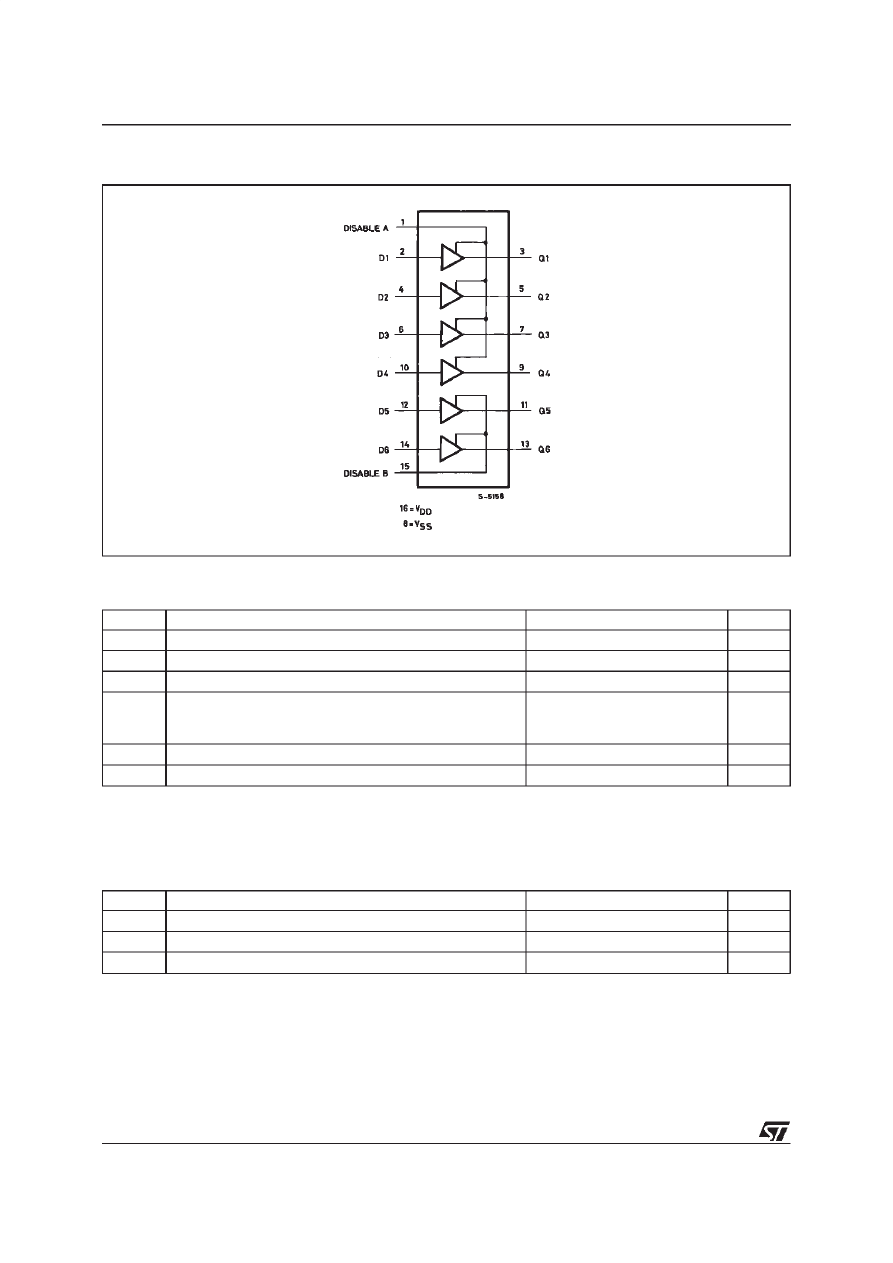
The HCF4503B is a hex noninverting buffer with
3-state
outputs
having
high
sink
and
source-current capability. Two disable controls
are provided, one of which controls four buffers
and the other controls the remaining two buffers.
PIN CONNECTION
SOP
DIP
ORDER CODES
PACKAGE
TUBE
T & R
DIP
HCF4503BEY
SOP
HCF4503BM1
HCF4503M013TR
1/10
FUNCTIONAL DIAGRAM
ABSOLUTE MAXIMUM RATING
Symbol
Parameter
Val ue
Unit
V
DD
*
Supply Voltage
-0.5 to +18
V
V
i
Input Voltage
-0.5 to V
DD
+ 0.5
V
I
I
DC Input Current (any one input)
±
10
mA
P
tot
Total Power Dissipation (per package)
Dissipation per Output Transistor
for Top = Full Package Temperature Range
200
100
mW
mW
T
op
Operating Temperature
-40 to +85
o
C
T
stg
Storage Temperature
-65 to +150
o
C
Stresses above those listedunder ”Absolute Maximum Ratings” may cause permanent damage to the device. This is a stress rating only and functional
operation ofthe device atthese or any other conditions above those indicated in the operational sections of this specification is not implied. Exposure to
absolute maximum ratingconditions for external periods may affect device reliability.
* Allvoltage values are referred to V
SS
pin voltage.
RECOMMENDED OPERATING CONDITIONS
Symbol
Parameter
Val ue
Unit
V
DD
Supply Voltage
3 to 15
V
V
I
Input Voltage
0 to V
DD
V
T
op
Operating Temperature
-40 to +85
o
C
HCF4503B
2/10
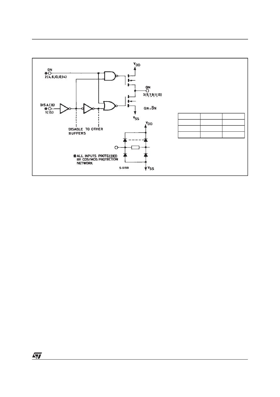
LOGIC DIAGRAM AND TRUTH TABLE
DN
DIS A (B)
Q N
0
0
0
1
0
1
X
1
High Z
X = Don’t care
HCF4503B
3/10
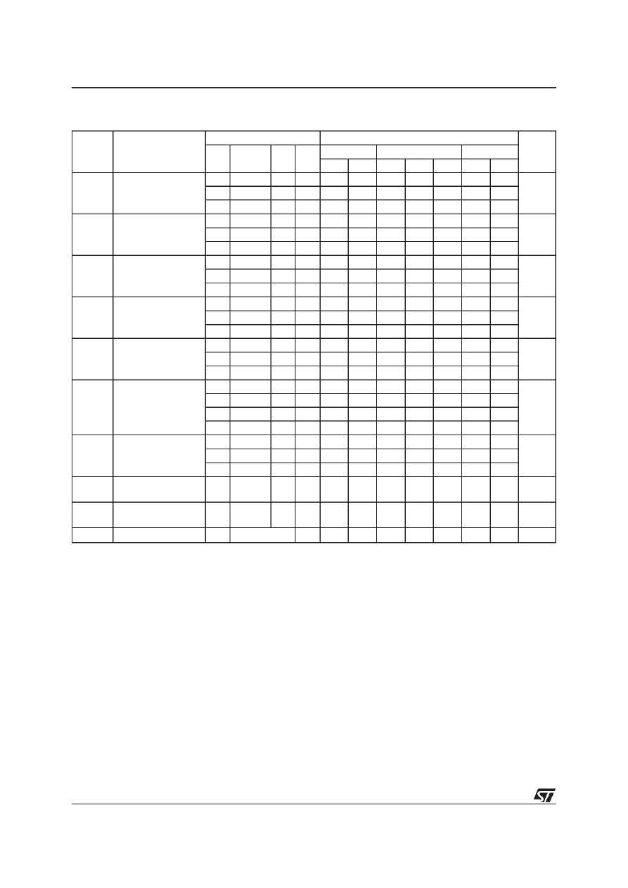
STATIC ELECTRICAL CHARACTERISTICS (over recommended operating conditions)
Symb ol
Parameter
T est Cond it ios
Valu e
Un it
V
I
(V)
V
O
(V)
| I
O
|
(
µ
A)
V
DD
(V)
-40
o
C
25
o
C
85
o
C
Mi n. Max. Min. T yp. Max. Min . Max.
I
L
Quiescent Current
0/5
5
4
0.02
4
30
µ
A
0/10
10
8
0.02
8
60
0/15
15
16
0.02
16
120
V
OH
Output High
Voltage
0/5
< 1
5
4.95
4.95
4.95
V
0/10
< 1
10
9.95
9.95
9.95
0/15
< 1
15
14.95
14.95
14.95
V
OL
Output Low
Voltage
5/0
< 1
5
0.05
0.05
0.05
V
10/0
< 1
10
0.05
0.05
0.05
15/0
< 1
15
0.05
0.05
0.05
V
IH
Input High
Voltage
0.5/4.5
< 1
5
3.5
3.5
3.5
V
1/9
< 1
10
7
7
7
1.5/13.5
< 1
15
11
11
11
V
IL
Input Low
Voltage
4.5/0.5
< 1
5
1.5
1.5
1.5
V
9/1
< 1
10
3
3
3
13.5/1.5
< 1
15
4
4
4
I
OH
Output Drive
Current
0/5
2.5
5
-4.8
-4.1
-5.2
-2.9
mA
0/5
4.6
5
-1
-0.8
-1.6
-0.6
0/10
9.5
10
-2.5
-2.2
-3.1
-1.6
0/15
13.5
15
-6.8
-5.8
-11.9
-4.2
I
OL
Output Sink Current
0/5
0.4
5
2.1
1.8
1.9
1.2
mA
0/10
0.5
10
5.4
4.7
5.3
3.3
0/15
1.5
15
16
13.7
19.5
9.7
I
IH
, I
IL
Input Leakage
Current
0/15
Any
Input
15
±
0. 3
±
10
-5
±
0. 3
±
1
µ
A
I
OZ
3-state Output
Leakage Current
0/15
Any
Input
15
±
1. 0
±
10
-4
±
1. 0
±
7.5
µ
A
C
I
Input Capacitance
Any Input
5
7.5
pF
TheNoise Margin for both ”1” and ”0” level is: 1V min.withV
DD
= 5 V, 2 V min.with V
DD
= 10 V, 2.5 V min. with V
DD
= 15 V
HCF4503B
4/10
DYNAMIC ELECTRICAL CHARACTERISTICS (T
amb
= 25
o
C, C
L
= 50 pF, R
L
= 200 K
Ω
,
typical temperaturecoefficent for all V
DD
values is 03 %/
o
C, all input rise and fall times= 20 ns)
Symb ol
Parameter
T est Cond ition s
Value
Un it
V
DD
(V)
Min.
Typ.
Max.
t
PLH
Propagation Delay Time
5
75
150
ns
10
35
70
15
25
50
t
PHL
Propagation Delay Time
5
55
110
ns
10
25
50
15
17
35
t
PHZ
t
PZH
3-State Propagation Delay Time
5
70
140
ns
10
30
60
15
25
50
t
PZL
t
PLZ
3-State Propagation Delay Time
5
90
180
ns
10
40
80
15
35
70
t
TLH
Transition Time
5
50
90
ns
10
30
45
15
25
35
t
THL
Transition Time
5
35
70
ns
10
20
40
15
13
25
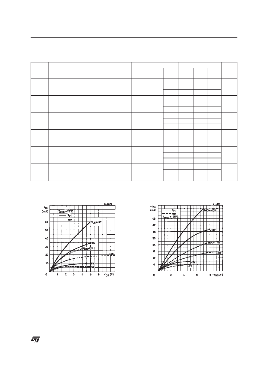
N-Channel Output Low (sink) Current
Characteristics.
P-Channel Output High (source) Current
Characteristics.
HCF4503B
5/10
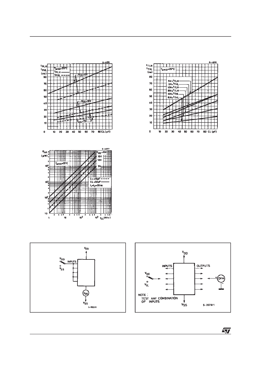
Typical Propagation Delay Time vs. Load
Capacitance.
Typical Transition Time vs. Load Capacitance.
Typical Dynamic Power Dissipation vs.
Input Voltage.
TEST CIRCUITS
Quiescent Device Current.
HCF4503B
6/10
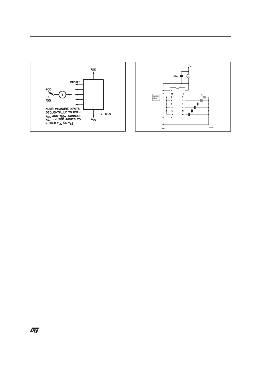
Input Leakage Current.
Dynamic Power Dissipation.
TEST CIRCUIT (continued)
HCF4503B
7/10
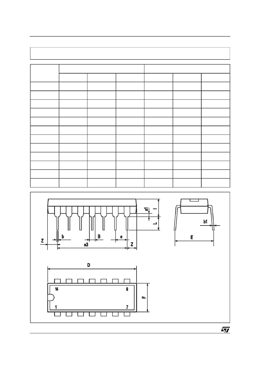
DIM.
mm
inch
MIN.
TYP.
MAX.
MIN.
TYP.
MAX.
a1
0.51
0.020
B
1.39
1.65
0.055
0.065
b
0.5
0.020
b1
0.25
0.010
D
20
0.787
E
8.5
0.335
e
2.54
0.100
e3
15.24
0.600
F
7.1
0.280
I
5.1
0.201
L
3.3
0.130
Z
1.27
2.54
0.050
0.100
P001A
Plastic DIP-14 MECHANICAL DATA
HCF4503B
8/10
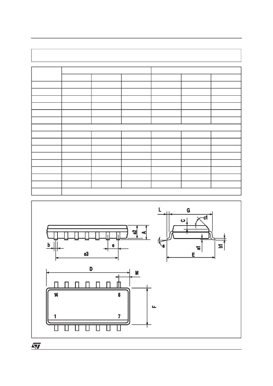
DIM.
mm
inch
MIN.
TYP.
MAX.
MIN.
TYP.
MAX.
A
1.75
0.068
a1
0.1
0.2
0.003
0.007
a2
1.65
0.064
b
0.35
0.46
0.013
0.018
b1
0.19
0.25
0.007
0.010
C
0.5
0.019
c1
45 (typ.)
D
8.55
8.75
0.336
0.344
E
5.8
6.2
0.228
0.244
e
1.27
0.050
e3
7.62
0.300
F
3.8
4.0
0.149
0.157
G
4.6
5.3
0.181
0.208
L
0.5
1.27
0.019
0.050
M
0.68
0.026
S
8 (max.)
P013G
SO-14 MECHANICAL DATA
HCF4503B
9/10

Information furnished is believed to be accurate and reliable. However, STMicroelectronics assumes no responsibility for the consequences
of use of such information nor for any infringement of patents or other rights of third parties which may result from its use. No license is
granted by implication or otherwise under any patent or patent rights of STMi croelectronics. Specification mentioned in this publication are
subject to change without notice. This publication supersedes and replaces all information previously supplied. STMi croelectronics products
are not authorized for use as critical components in life support devices or systems withoutexpress written approval of STMicroelectronics.
The ST logo is a registered trademark of STMicroelectronics
2000 STMicroelectronics – Printed in Italy – All Rights Reserved
STMicroelectronics GROUP OF COMPANIES
Australia - Brazil - China - Finland - France - Germany - Hong Kong - India - Italy - Japan - Malaysia - Malta - Morocco
Singapore - Spain - Sweden - Switzerland - United Kingdom - U.S.A.
http://www.st.com
.
HCF4503B
10/10
Wyszukiwarka
Podobne podstrony:
4503, Akademia Morska, Atlantic United Marine
4503
praca-licencjacka-b7-4503, Dokumenty(8)
4503
03 swiat sg rysunkiid 4503 Nieznany
4503
4503
4503
4503
D H 1 RZN 4503 T
więcej podobnych podstron